

Raytheon RMPA0951A-102 Datasheet
Raytheon RF Components
362 Lowell Street
Andover, MA 01810
Revised March 29, 2002
Page 1
www.raytheonrf.com
PRODUCT INFORMATION
Characteristic performance data and specifications are subject to change without notice.
RMPA0951A-102
3V Cellular CDMA Power Amplifier Module
Description
Parameter Min Typ Max Unit
Frequency Range 824 849 MHz
Gain (Pout=+28 dBm) 30 dB
Gain AMPS (Pout=+31.5dBm) 30 dB
Analog Output Power 31.5 dBm
Power-Added Efficiency
CDMA (Pout =+28 dBm) 30 35 %
Analog (Pout =+31.5 dBm) 44 50 %
ACPR1
5
-52 -46 dBc
ACPR2
5
-58 -55 dBc
Rx-Band Noise Power
(All Power Levels) -135 dBm/Hz
Single positive-supply operation
High dual-mode (AMPS/CDMA) efficiency
Excellent linearity
Small size: 6.0 x 6.0 x 1.5 mm
3
LCC package
50-ohm matched input and output module
Adjustable quiescent current and power-down mode
Suitable for CDMA and CDMA2000 1X systems
Features
Notes:
1. No permanent damage with only one parameter set at extreme limit and other parameters typical.
2. Typical RF input powers for CDMA (-3 dBm) and AMPS mode (+2 dBm) operation.
3. All parameters to be met at Ta = +25°C, Vcc = +3.5V, Vref=3.0V and load VSWR ≤ 1.2:1.
4. Load VSWR ≤ 6:1 all phase angles.
5. CDMA Waveform measured using the ratio of the average power within the 1.23 MHz signal channel to the power within a
30 kHz resolution bandwidth, Pout=28 dBm. Offset is ± 885 KHz, ± 1.98 MHz.
6. No applied RF signal. Vcc=+3.5V nominal, Vref=+0.2V maximum.
7. Guaranteed by design.
Electrical
Characteristics
3
Parameter Min Typ Max Unit
Noise Figure 3 dB
Input VSWR (50Ω) 1.5:1 2.5:1 --Output VSWR (50Ω) 2.5:1 --Stability (All spurious)
4,7
-60 dBc
Harmonics (Po ≤ 28 dBm)
7
2fo, 3fo, 4fo -30 dBc
Quiescent Current 80 100 mA
Power Shutdown Current
6
210uA
Vcc 3.0 3.5 4.0 Volts
Vref 2.0 3.0 3.2 Volts
Iref 16 mA
The RMPA0951A-102 is a dual mode, small-outline Power Amplifier Module (PAM) for Cellular CDMA personal
communication system applications. The PA is internally-matched to 50 ohms and DC blocked which minimizes the
use of external components and reduces circuit complexity for system designers. High AMPS/CDMA efficiency and
good linearity are achieved using Raytheon RF Components’ InGaP Heterojunction Bipolar Transistor (HBT)
process.
Parameter Symbol Value Vnits
Supply Voltage Vc1, Vc2 6.0 V
Reference Voltage Vref 1.5 to 4.0 V
RF Input Power
2
Pin +7 dBm
Load VSWR VSWR 6:1
Case Operating Temperature Tc -30 to +85 °C
Storage Temperature Tstg -55 to +150 °C
Absolute
Maximum
Ratings
1
Raytheon RF Components
362 Lowell Street
Andover, MA 01810
Revised March 29, 2002
Page 2
www.raytheonrf.com
PRODUCT INFORMATION
Characteristic performance data and specifications are subject to change without notice.
RMPA0951A-102
3V Cellular CDMA Power Amplifier Module
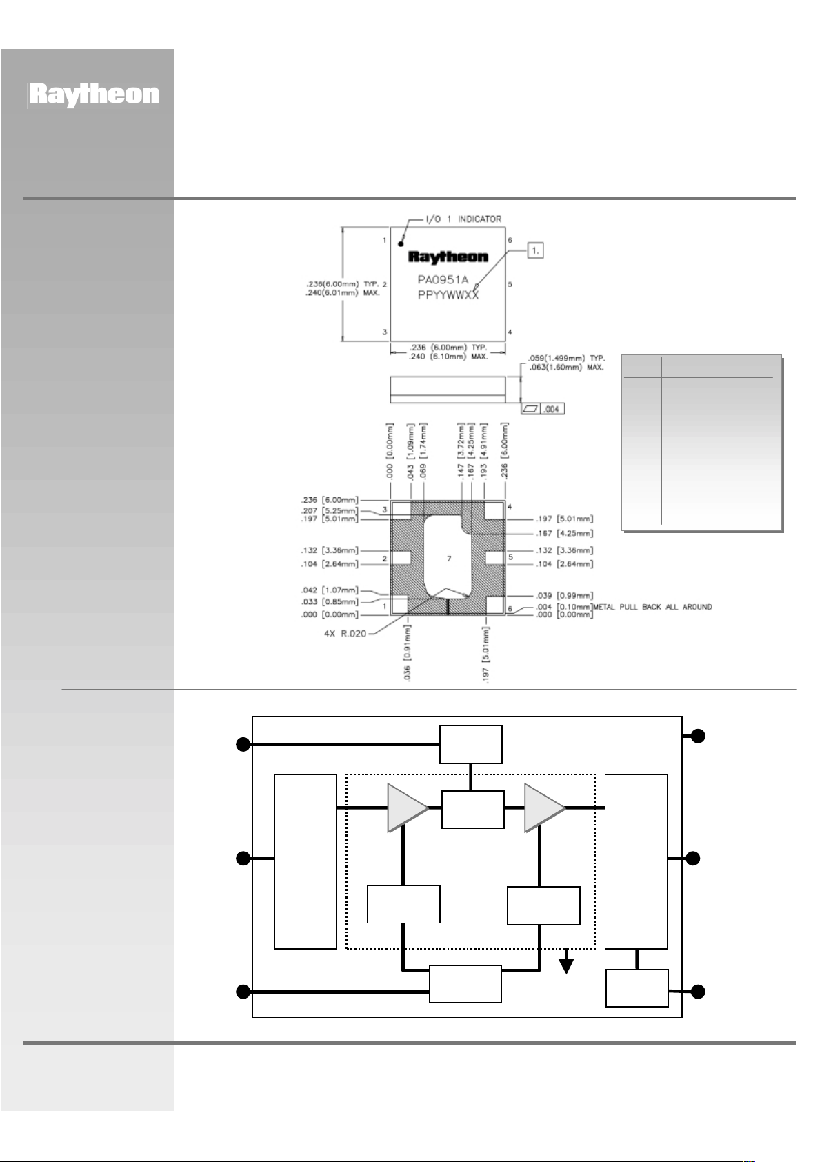
Figure 2
Functional Block
Diagram
RF IN
(2)
Vref
(3)
INPUT
STAGE
OUTPUT
STAGE
MMIC
PA MODULE
GND (Pin 7)(Package Bias)
RF OUT
(5)
Vcc1
(1)
N/C (6)
Vcc2
(4)
(TOPSIDE VIEW)
Vcc=3.5V (nom)
Vref=3.0V (nom)
824-849 MHz
50 Ohms I/O
COLLECTOR
BIAS 2
INTERSTAGE
MATCH
COLLECTOR
BIAS 1
Figure 1
Package Outline and
Pin Designations
INPUT STAGE
BIAS
OUTPUT STAGE
BIAS
REFERENCE
ADJUST
OUTPUT
MATCHING
NETWORK
INPUT
MATCHING
NETWORK
Dimensions in inches (mm)
Vcc
RF IN
Vref
Vcc2
RF OUT
N/C
GND
1
2
3
4
5
6
7
DescriptionPin #
Raytheon RF Components
362 Lowell Street
Andover, MA 01810
Revised March 29, 2002
Page 3
www.raytheonrf.com
PRODUCT INFORMATION
Characteristic performance data and specifications are subject to change without notice.
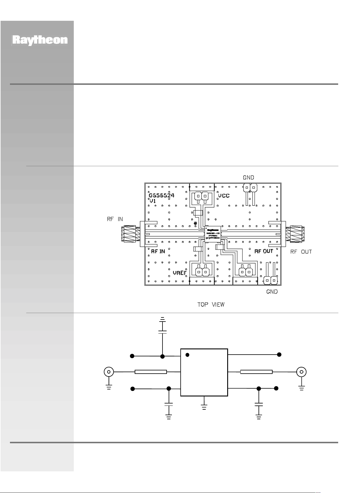
PCB Specifications:
Material: Rogers RO4003
Dimensions: 2.0”x1.5”x0.032”
Metallization: 1/2 oz Copper Cladding
With device marking oriented right side up, RF IN is on the left and RF OUT is on the right.
Vcc= +3.5V nominal. Vref=+ 3.0V nominal to obtain Iccq= 80 mA. Operation at lower or higher quiescent currents
can be achieved by decreasing or increasing Vref voltage relative to +3.0V.
First ground the PCB (GND terminal) and apply +3.5V to the collector supply terminals (Vcc1, Vcc2). Next apply
+3.0V to the reference supply (Vref terminal). Quiescent collector current with no RF applied will be about 80 mA.
Reference supply current with or without RF applied will be about 15 mA. When turning amplifier off, reverse
power supply sequence.
Apply -20 dBm RF input power at Cellular frequency (824-849 MHz). After making any initial small signal
measurements at this drive level, input power may be increased up to a maximum of +7 dBm for large signal,
analog (AMPS) or digital CDMA measurements. Do not exceed +7 dBm input power.
Figure 3
Evaluation Board
Layout, Schematic,
and Instructions
* Minimum bypass capacitance recommended for best linearity/low-noise performance.
RMPA0951A-102
3V Cellular CDMA Power Amplifier Module
C1 *
3.3 µF
2
34
5
6
7
1
Vcc1
SMA1
RF IN
SMA2
RF OUT
Vref
N/C
Vcc2
*
(package base)
50 ohm TRL
50 ohm TRL
C2 *
3.3 µF
Raytheon
RMPA0951A-102
PPYYWWZZZ
C3 *
1000 pF
Note: Addition of C3 bypass
capacitor on Vref pin recommended
to minimize Rx band noise.
PCB Schematic
Vcc1
Vref Vcc2
Raytheon RF Components
362 Lowell Street
Andover, MA 01810
Revised March 29, 2002
Page 4
www.raytheonrf.com
PRODUCT INFORMATION
Characteristic performance data and specifications are subject to change without notice.
RMPA0951A-102
3V Cellular CDMA Power Amplifier Module
Application
Information
Precautions to Avoid Permanent Device Damage:
– Cleanliness: Observe proper handling procedures to ensure clean devices and PCBs. Devices should
remain in their original packaging until component placement to ensure no contamination or damage to RF,
DC & ground contact areas.
– Device Cleaning: Standard board cleaning techniques should not present device problems provided that
the boards are properly dried to remove solvents or water residues.
– Static Sensitivity: Follow ESD precautions to protect against ESD damage:
• A properly grounded static-dissipative surface on which to place devices.
• Static-dissipative floor or mat.
• A properly grounded conductive wrist strap for each person to wear while handling devices.
– General Handling: Handle the package on the top with a vacuum collet or along the edges with a sharp
pair of bent tweezers. Avoiding damaging the RF, DC, & ground contacts on the package bottom. Do not
apply excessive pressure to the top of the lid.
– Device Storage: Devices are supplied in heat-sealed, moisture-barrier bags. In this condition, devices are
protected and require no special storage conditions. Once the sealed bag has been opened, devices should
be stored in a dry nitrogen environment.
Device Usage: Raytheon recommends the following procedures prior to assembly.
• Dry-bake devices at 125
°C for 24 hours minimum. Note: The shipping trays cannot withstand 125°C
baking temperature.
• Assemble the dry-baked devices within 7 days of removal from the oven.
• During the 7-day period, the devices must be stored in an environment of less than 60% relative
humidity and a maximum temperature of 30
°C
• If the 7-day period or the environmental conditions have been exceeded, then the dry-bake procedure
must be repeated.
Solder Materials & Temperature Profile: Reflow soldering is the preferred method of SMT attachment. Hand
soldering is not recommended.
– Reflow Profile
• Ramp-up: During this stage the solvents are evaporated from the solder paste. Care should be taken to
prevent rapid oxidation (or paste slump) and solder bursts caused by violent solvent out-gassing. A
typical heating rate is 1- 2°C/sec.
• Pre-heat/soak: The soak temperature stage serves two purposes; the flux is activated and the board
and devices achieve a uniform temperature. The recommended soak condition is: 120-150 seconds at
150°C.
• Reflow Zone: If the temperature is too high, then devices may be damaged by mechanical stress due to
thermal mismatch or there may be problems due to excessive solder oxidation. Excessive time at
temperature can enhance the formation of inter-metallic compounds at the lead/board interface and
may lead to early mechanical failure of the joint. Reflow must occur prior to the flux being completely
driven off. The duration of peak reflow temperature should not exceed 10 seconds. Maximum soldering
temperatures should be in the range 215-220°C, with a maximum limit of 225°C.
• Cooling Zone: Steep thermal gradients may give rise to excessive thermal shock. However, rapid
cooling promotes a finer grain structure and a more crack-resistant solder joint. Figure 1 indicates the
recommended soldering profile.
Solder Joint Characteristics: Proper operation of this device depends on a reliable void-free attachment of the
heatsink to the PWB. The solder joint should be 95% void-free and be a consistent thickness.
Rework Considerations: Rework of a device attached to a board is limited to reflow of the solder with a heat
gun. The device should not be subjected to more than 225°C and reflow solder in the molten state for more than
5 seconds. No more than 2 rework operations should be performed.
Raytheon RF Components
362 Lowell Street
Andover, MA 01810
Revised March 29, 2002
Page 5
www.raytheonrf.com
PRODUCT INFORMATION
Characteristic performance data and specifications are subject to change without notice.
25.00
26.00
27.00
28.00
29.00
30.00
31.00
32.00
33.00
34.00
35.00
0.0 4.0 8.0 12.0 16.0 20.0 24.0 28.0
Out put Power ( dBm )
Gain (dB)
824 MHz ( +2 5C)
836.5 M Hz (+25C)
849 MHz ( +2 5C)
824 MHz ( +8 5C)
836.5 M Hz (+85C)
849 MHz ( +8 5C)
824 MHz ( - 30C)
836.5 M Hz (-30C)
849 MHz ( - 30C)
RMPA0951A-102
3V Cellular CDMA Power Amplifier Module
Figure 4
Recommended Solder
Reflow Profile
Soak at
150
o
C for
60 Sec
45 Sec
(Max)
above
183
o
C
1
o
C/Sec
183
o
C
10 Sec
1oC/Sec
0
20
40
60
80
100
120
140
160
180
200
220
240
0 60 120 180 240 300
Time (Sec)
Deg C
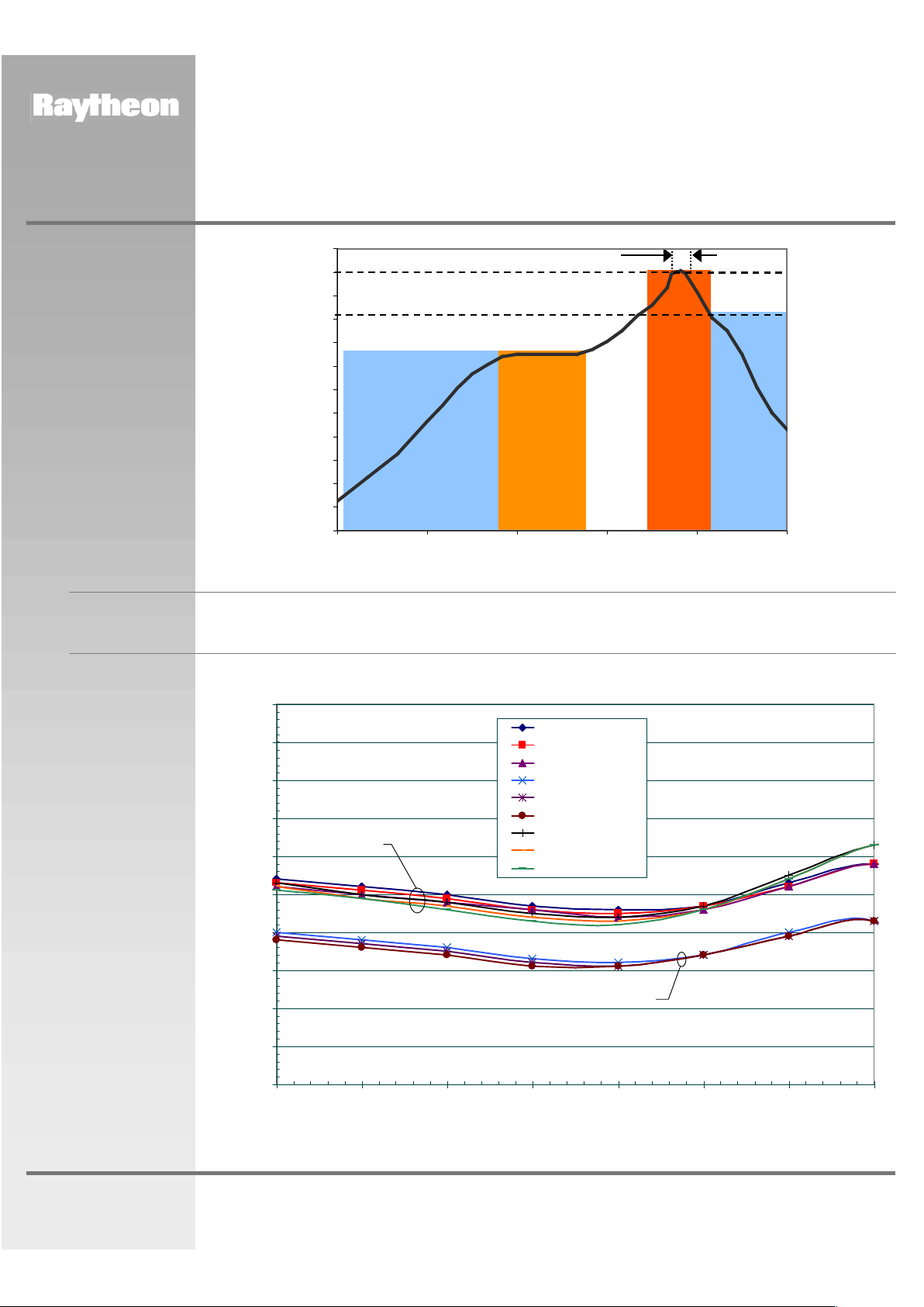
Performance
Data
Measured performance for typical production amplifiers is represented in the figures below. Key characteristics
such as gain, efficiency, output power and linearity are shown for both AMPS and CDMA operation.
Figure 5
RMPA0951A-102 CDMA Gain vs Pout, Frequency and Temperature
+25°C, -30°C
+85°C
 Loading...