

Raytheon RMPA0951-102 Datasheet
Raytheon RF Components
362 Lowell Street
Andover, MA 01810
Revised May 10, 2001
Page 1
www.raytheon.com/micro
ADVANCED INFORMATION
Characteristic performance data and specifications are subject to change without notice.
RMPA0951-102
3V Cellular CDMA Power Amplifier Module
Description
Parameter Min Typ Max Unit
Frequency Range 824 849 MHz
CDMA Gain
(Pout=0 dBm) 29.5 dB
(Pout=+28 dBm) 31 dB
Analog Output Power 31.5 dBm
AMPS Gain (Pout=+31.5 dBm) 29
Power-Added Efficiency
CDMA (Pout =+28 dBm) 32 %
Analog (Pout =+31.5 dBm) 46 %
ACPR (Pout=+28 dBm)
5
-49 dBc
Noise Figure 5 6 dB
Single positive-supply operation.
High dual-mode (AMPS/CDMA) efficiency and good linearity
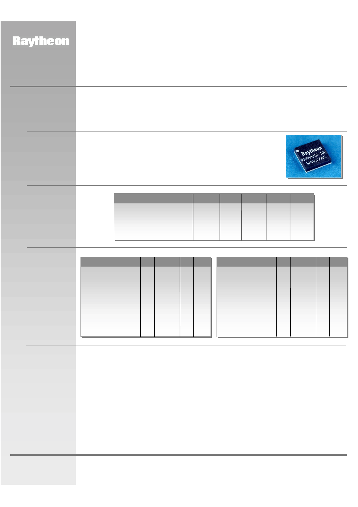
Small size: 6.0 x 6.0 x 1.5 mm
3
LCC package.
50-ohm matched input and output module.
Adjustable quiescent current and power-down mode.
Features
Notes:
1. No permanent damage with only one parameter set at extreme limit. Other parameters at typical values.
2. Typical RF input power for +28 dBm CDMA (-3 dBm) and +31.5 dBm AMPS-Mode output powers.
3. All parameters to be met at Ta = +25°C, Vcc = +3.5V, Vref=3.0V and load VSWR ≤ 1.2:1.
4. Load VSWR ≤ 6:1 all phase angles.
5. CDMA Waveform measured using the ratio of the average power within the 1.23 MHz signal channel to the power within a
30 kHz resolution bandwidth at a 885 KHz offset.
6. No applied RF signal. Vcc=+3.5V nominal, Vref=+0.2V maximum.
Electrical
Characteristics
3
Parameter Min Typ Max Unit
Rx-Band Noise Power
(All Power Levels) -135 dBm/Hz
Input VSWR (50Ω) 2.0:1 2.5:1 --Output VSWR (50Ω) 3.5:1 --Stability (All spurious)
4
-70 dBc
Harmonics (Po ≤ 28 dBm)
2fo, 3fo, 4fo -30 dBc
Quiescent Current 70 100 mA
Power Shutdown Current
6
210uA
Vcc 3.0 3.5 4.0 Volts
Vref 2.0 3.0 3.2 Volts
Case Operating Temp -30 +85 °C
The RMPA0951-102 is a dual mode, small-outline power amplifier module (PAM) for Cellular CDMA personal
communication system applications. The PA is internally-matched to 50 ohms and DC blocked which minimizes the
use of external components and reduces circuit complexity for system designers. High AMPS/CDMA efficiency and
good linearity are achieved using Raytheon’s Heterojunction Bipolar Transistor (HBT) process.
(Photo)
Parameter Symbol Min Typical Max Units
Supply Voltage Vc1, Vc2 3.5 6.0 V
Reference Voltage Vref 1.5 3.0 4.0 V
RF Input Power
2
Pin -3/+2 +7 dBm
Load VSWR VSWR 1.2:1 10:1
Case Operating Temperature Tc -40 +25 +110 °C
Storage Temperature Tstg -55 +25 +150 °C
Absolute
Maximum
Ratings
1
Raytheon RF Components
362 Lowell Street
Andover, MA 01810
Revised May 10, 2001
Page 2
www.raytheon.com/micro
ADVANCED INFORMATION
Characteristic performance data and specifications are subject to change without notice.
RMPA0951-102
3V Cellular CDMA Power Amplifier Module
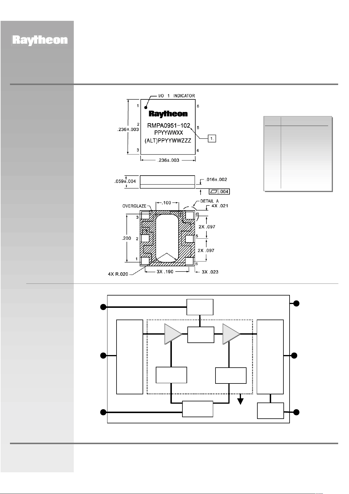
Functional
Block
Diagram
RF IN
(2)
VREF
(3)
INPUT
STAGE
OUTPUT
STAGE
MMIC
PA MODULE
GND (Pin 7)(Package Bias)
RF OUT
Vcc1
(1)
N/C (6)
Vcc2
(4)
(TOPSIDE VIEW)
VCC=3.5V (nom)
VREF=3.0V (nom)
824-849 MHz
50 Ohms I/O
COLLECTOR
BIAS 2
INTERSTAGE
MATCH
COLLECTOR
BIAS 1
Package
Information
Vcc1
RF IN
VREF
Vcc2
RF OUT
N/C
GND
1
2
3
4
5
6
7
DescriptionPin #
INPUT STAGE
BIAS
OUTPUT STAGE
BIAS
REFERENCE
ADJUST
OUTPUT
MATCHING
NETWORK
INPUT
MATCHING
NETWORK
Dimensions in inches (mm)
(6.0)
(6.0)
(1.5)
(2.46)
(5.08)
(2.54)
(4.82)
Raytheon RF Components
362 Lowell Street
Andover, MA 01810
Revised May 10, 2001
Page 3
www.raytheon.com/micro
ADVANCED INFORMATION
Characteristic performance data and specifications are subject to change without notice.
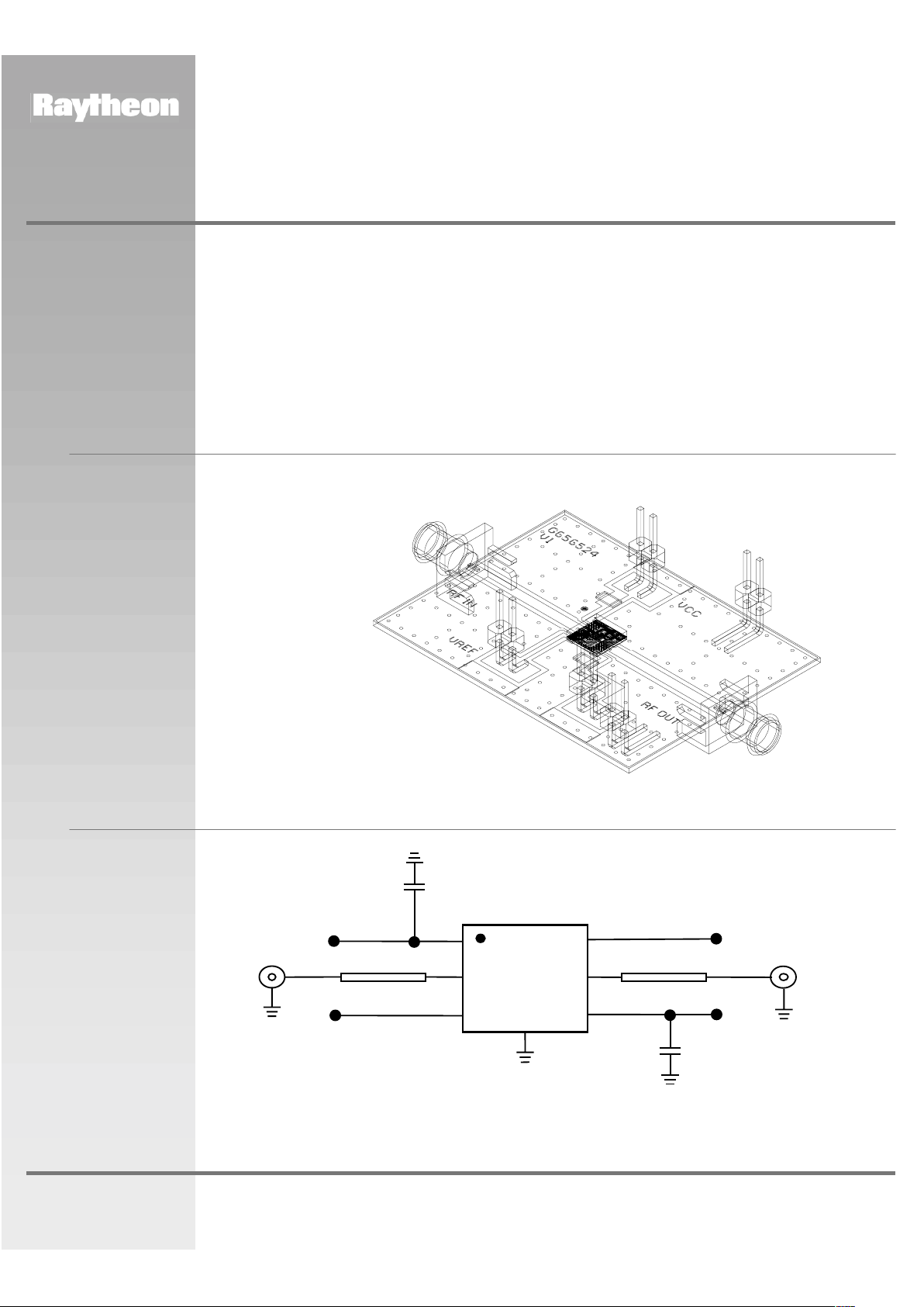
VREF
RF IN
VCC
RF OUT
GND
PCB Specifications:
Material: Rogers RO4003
Dimensions: 2.0”x1.5”x0.032”
Metallization: 1/2 OZ Copper Cladding
With device marking oriented right side up, RF IN is on the left and RF OUT is on the right.
VCC= +3.5V nominal. Vref=+ 3.0V nominal to obtain Iccq= 70 mA. Operation at lower or higher quiescent
currents can be achieved by decreasing or increasing Vref voltage relative to +3.0V.
First ground the PCB (GND terminal) and apply +3.5V to the collector supply terminals (VCC1, VCC2). Next
apply +3.0V to the reference supply (VREF terminal). Quiescent collector current with no RF applied will be
about 80 mA. Reference supply current with or without RF applied will be about 15 mA. When turning amplifier
off, reverse power supply sequence.
Apply -20 dBm RF input power at Cellular frequency (824-849 MHz). After making any initial small signal
measurements at this drive level, input power may be increased up to a maximum of +7 dBm for large signal,
analog (AMPS) or digital CDMA measurements. Do not exceed +7 dBm input power.
Evaluation Board
Layout, Schematic,
and Instructions
C1 *
3.3 µF
*Minimum VCC bypass capacitance recommended
for best RF performance.
2
34
5
6
7
1
Vcc1
SMA1
RF IN
SMA2
RF OUT
Vref
N/C
Vcc2
*
(package base)
50 ohm TRL
50 ohm TRL
C2 *
3.3 µF
RMPA0951-102
3V Cellular CDMA Power Amplifier Module
Raytheon
RMPA0951-102
PPYYWWZZZ
 Loading...