

Raytheon RMPA0913C-58 Datasheet
RMPA0913C-58
3.5V AMPS/CDMA Power Amplifier
PRODUCT INFORMATION
Description
Features
Absolute
Maximum
Ratings
The RMPA0913C-58 is a monolithic high efficiency power amplifier for AMPS/CDMA dual mode applications in the
824 to 849 MHz frequency band. Performance parameters may be slightly adjusted by “tweaking” off-chip
matching components. The amplifier circuit design is a single ended configuration that utilizes harmonic tuning for
increased power added efficiency and linearity.The device uses Raytheon’s Pseudomorphic High Electron Mobility
Transistor (pHEMT) process.
Positive supply voltage of 3.5V, nominal
Power Added Efficiency of 56%, typical, at power out of 31.5 dBm
Power Added Efficiency of 40%, typical, for CDMA power out of 28.5 dBm
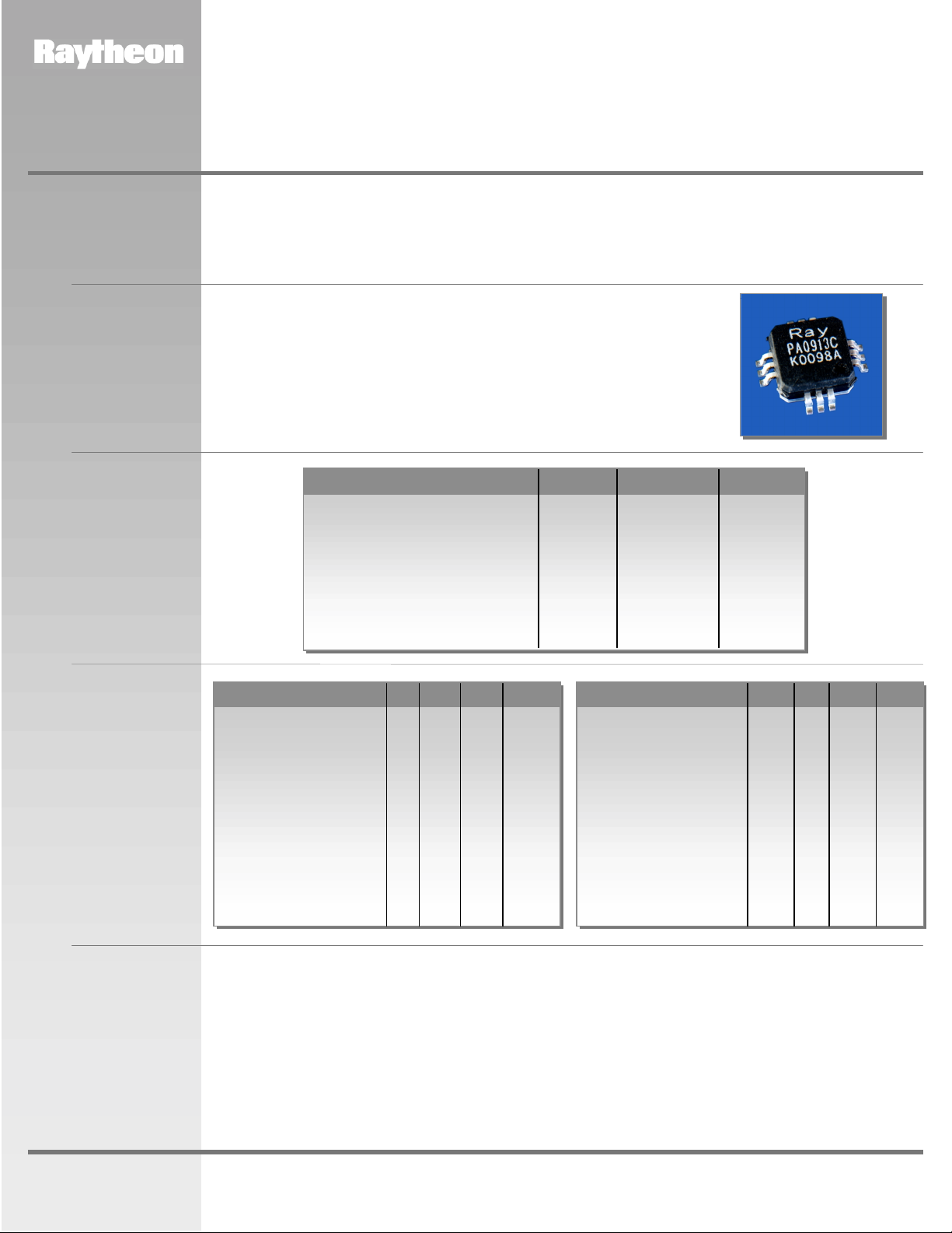
Small outline metal based quad plastic package
Parameter Symbol Value Units
Positive DC Voltage Vd1,Vd2 + 9 Volts
Negative DC Voltage Vg1,Vg2 - 6 Volts
Simultaneous (Vd-Vg) Vdg +12 Volts
RF Input Power (from 50-Ohm source) P
Operating Case Temperature (Case) T
Storage Temperature Range T
Thermal Resistance RTj-c 15 °C/W
+10dBm
IN
C
Stg
-30 to 110 °C
-35 to 110 °C
Electrical
Characteristics
(Specifications at
o
C operating free
25
air temperature
unless otherwise
stated)
Parameter Min Typ Max Unit
Frequency Range 824 849 MHz
Gain (Small Signal) 30 dB
Gain Variation vs Temp -0.02 dB/°C
Gain Linearity
(0 dBm ≤ Pout ≤ 28.5 dBm) -1.5 +0.0 dB
Noise Power (869-894 MHz) -140 dBm/Hz
Input VSWR (50Ω) 2.0:1 --Stability (All spurious)
Harmonics (Po ≤ 31.5 dBm) -35 dBc
Power Out
Vdd=3.5V, Pin=7 dBm 32.5 dBm
Notes:
1. Source/Load VSWR (All Angles) ≤ 3:1 In-Band, Load VSWR (All Angles) ≥ 20:1 Out of Band, Valid over Case Operating Temperature Range.
2. Po ≤ 28.5 dBm at Vdd=3.5V; CDMA Waveform measured using the ratio of the average power within a 1.23 MHz channel and within a 30
kHz bandwidth at the specified offset.
3. Vg1 adjusted for Idq (stage 1) = 35 mA, Vg2 adjusted for Idq (stage 2) = 155 mA.
Characteristic performance data and specifications are subject to change without notice.
1
-70 dBc
Parameter Min Typ Max Unit
Efficiency
Pin = 7 dBm, Vdd= 3.5V 62 %
Po = 31.5 dBm, Vdd = 3.5V 56 %
Po = 28.5 dBm , Vdd= 3.5V 40 %
Po = 10 dBm , Vdd= 3.5V 1.5 %
2
ACPR
(Offset ≥ ± 900 kHz) 48 dBc
(Offset ≥ ± 1.98 MHz) 63 dBc
Noise Figure (over temp) 4.5 dB
Vdd 3.5 Volts
Vg1, Vg2 (<4 mA)
Case Operating Temp -40 +85 °C
3
-1.75 -0.25 Volts
www.raytheon.com/micro
Revised March 30, 2000
Page 1
Raytheon RF Components
362 Lowell Street
Andover, MA 01810
RMPA0913C-58
3.5V AMPS/CDMA Power Amplifier
PRODUCT INFORMATION
Application
Information
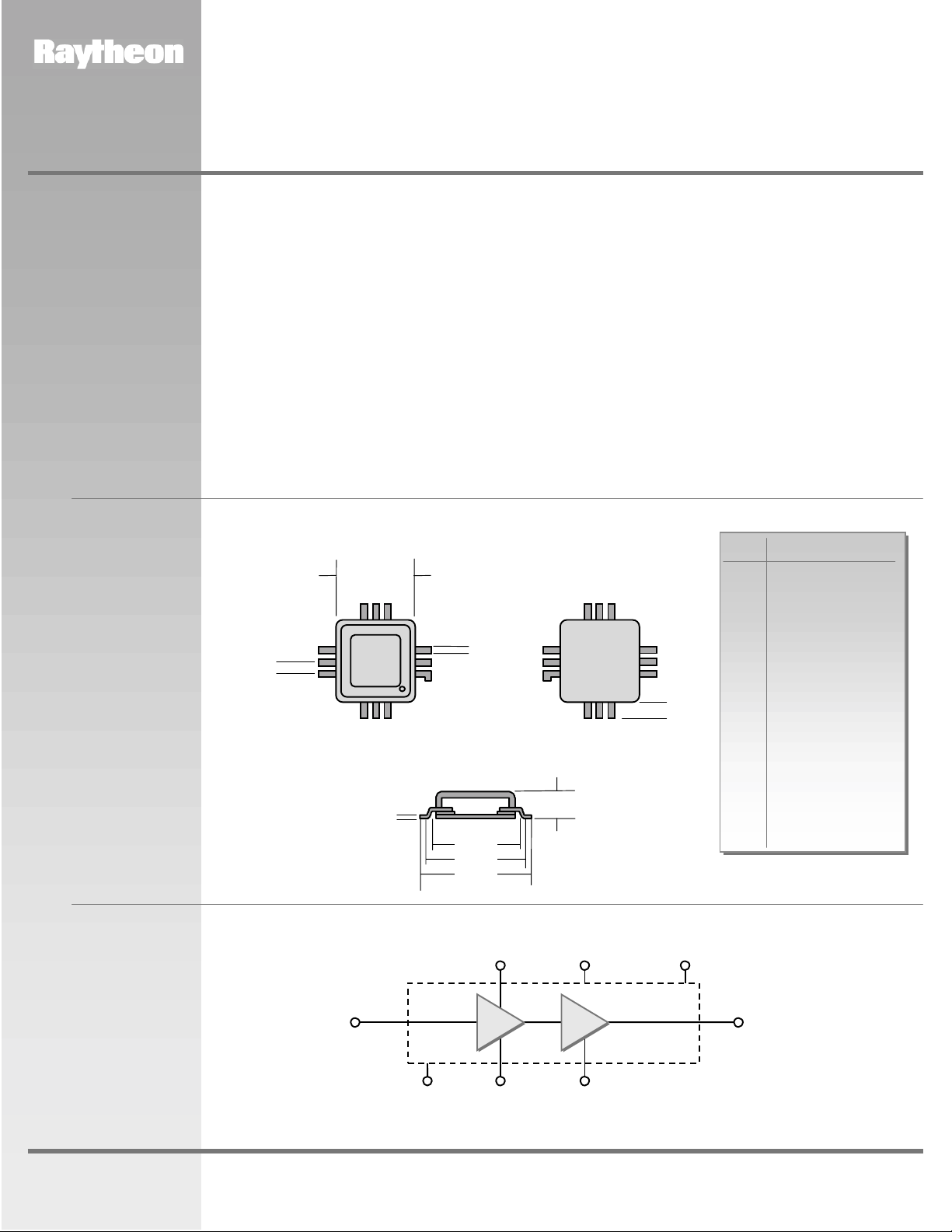
Figure 1
Package Information
CAUTION: THIS IS AN ESD SENSITIVE DEVICE.
The following describes a procedure for evaluating the Raytheon RMPA0913C-58, a monolithic high efficiency
power amplifier, in a surface mount package, designed for use in the AMPS/CDMA dual mode portable phones.
Figure 1 shows the package outline and pin designations. Figure 2 shows the functional block diagram of the
packaged product. It should be noted that the amplifier requires external passive components for DC bias and RF
input and output matching circuits. A recommended schematic is shown in figure 3. The gate biases for the two
stages of the amplifier are set by simple on-chip circuits. Figure 4 shows a typical layout of an evaluation board
(RMPA0913C-58-TB), corresponding to the schematic circuit of figure 3. The following should be noted:
(1) Pin designations and their functions are as shown
in figure 1 and Table 1.
(2) Vg1, Vg2 are denoted as the Gate Voltages
(negative) applied at the pins of the package
(4) Vd1, Vd2 are denoted as the Drain Voltages
(positive) applied at the pins of the package
(5) Vdd1, Vdd2 are denoted as the positive supply
voltages at the evaluation board terminals
(3) Vgg1, Vgg2 are denoted as the negative supply
voltages at the evaluation board terminals
Note: The two drain voltages are tied to the same terminal denoted as Vdd on the evaluation board
Dimensions in inches
0.030
TOP VIEW
0.200 SQ.
456
A
7
8
RAY
RMBA
0913C-58
9
10
11
0.010
3
0.015
2
1
12
PLASTIC LID
0.230
0.246
0.282
BOTTOM VIEW
3
2
1
12
0.069 MAX.
SIDE SECTION
456
13
11
10
7
8
9
0.041
DescriptionPin #
RF Out & Vd2
1
RF Out & Vd2
2
RF Out & Vd2
3
AC Ground (g2)
4
GND
5
AC Ground (g1)
6
GND
7
RF Input
8
GND
9
Vd1
10
Vg2
11
Vg1
12
GND (METAL BASE)
13
Figure 2
Functional Block
Diagram of
Packaged Product
www.raytheon.com/micro
Vd1
Pin# 10
RF IN
Pin# 8
AC Ground (g1)
Pin# 6
Characteristic performance data and specifications are subject to change without notice.
Revised March 30, 2000
Page 2
Vg1
Pin# 12
Ground
Pin# 5, 7, 9, 13
Vg2
Pin# 11
AC Ground (g2)
Pin# 4
RF OUT & Vd2
Pin# 1, 2, 3
Raytheon RF Components
362 Lowell Street
Andover, MA 01810
 Loading...