

Page 1

V ersion: A
Issued Date: 2016/11/25
Approval Sheet
(產品承認書)
產品名稱 (Product): BT 4.2 Module (nRF52832)
產品型號 (Model No.): MDBT42 & MDBT42-P Series
Page 2

Index
1. Overall Introduction ...................................................................................................... 3
1.1. Application ............................................................................................................ 3
1.2. Features ............................................................................................................... 4
1.3. Profile & Service Information ................................................................................ 5
2. Product Dimension ....................................................................................................... 6
2.1. PCB Dimensions & Pin Indication ......................................................................... 6
2.2. Recommended Layout of Solder Pad ................................................................... 8
2.3. RF Layout Suggestion (aka Keep-Out Area) ...................................................... 12
2.4. Footprint & Design Guide ................................................................................... 12
2.5. Pin Assignment ................................................................................................... 13
2.6. GPIO Located Near the Radio ............................................................................ 15
3. Main Chip Solution ...................................................................................................... 15
4. Specification ................................................................................................................ 16
4.1. Absolute Maximum Ratings ................................................................................ 16
4.2. Operation Conditions .......................................................................................... 16
4.3. Electrical Specifications ...................................................................................... 17
5. FCC Compliance .......................................................................................................... 22
6. IC Caution .................................................................................................................... 24
7. NCC
警語 ...................................................................................................................... 25
Page 3

1. Overall Introduction
Raytac’s MDBT42 & MDBT42-P is a BT 4.0, BT 4.1 and BT 4.2 stack (Bluetooth low energy
or BLE) module designed based on Nordic nRF52832 SoC solution, which incorporates:
GPIO, SPI, UART, I2C, I2S, PWM and ADC interfaces for connecting peripherals and
sensors.
Features of the module:
1. Dual Transmission mode of BLE & 2.4Ghz RF upon customer preference.
2. Compact size with (L) 13.8 x (W) 8.8 x (H) 1.9 mm.
3. Low power requirements, ultra-low peak, average and idle mode power consumption.
4. Be compatible with a large installed base of mobile phones, tablets and computers.
5. Fully coverage of BLE software stack. See 1.3 Profile & Service Information.
6. BLE & RF transmission switching helps products fit all operation system and most
hardware.
1.1. Application
•IoT
•Home automation
•Sensor networks
•Building automation
•Personal Area Networks
•Health / fitness sensor and monitor device
•Medical devices
•Key-fobs and wrist watches
•Interactive entertainment devices
•Remote control
•Gaming controller
•Beacons
•A4WP wireless chargers and devices
•Remote control toys
•Computer peripherals and I/O devices
•Mouse
•Keyboard
•Multi-touch trackpad
3
Page 4

1.2. Features
•Multi-protocol 2.4GHz radio
•ARM® Cortex®-M4 32-bit processor with FPU, 64 MHz
•512KB flash programmed memory and 64KB RAM
•Software stacks available as downloads
•Application development independent from protocol stack
•On-air compatible with nRF51, nRF24AP and nRF24L series
•Programmable TX output power from -20dBm to +4dBm in 4dB steps
•RSSI
•RAM mapped FIFOs using EasyDMA
•Dynamic on-air payload length up to 256 bytes
•Flexible and configurable 32 pin GPIO
•Programmable peripheral interface - PPI
•Simple ON / OFF global power mode
•Full set of digital interface all with Easy DMA including:
•3 x Hardware SPI master ; 3 x Hardware SPI slave
•2 x two-wire master ; 2 x two-wire slave
•1 x UART (CTS / RTS)
•PDM for digital microphone
•I2S for audio
•Quadrature demodulator
•12-bit / 200KSPS ADC
•128-bit AES ECB / CCM / AAR co-processor
•Lowe cost external crystal 32MHz ± 40ppm for Bluetooth ; ± 50ppm for ANT Plus
•Lowe power 32MHz crystal and RC oscillators
•Wide supply voltage range 1.7V to 3.6V
•On-chip DC/DC buck converter
•Individual power management for all peripherals
•Timer counter
•5 x 32-bit
•3 x 24-bit RTC
•NFC-A tag interface for OOB pairing
•3x 4-channel pulse width modulator (PWM) units with EasyDMA
4
Page 5

1.3. Profile & Service Information
Profile & Service are supported by MDBT42 & MDBT42-P as below:
Profile Description Service Description
Alert Notification Profile Alert Notification Service
Blood Pressure Service
Blood Pressure Profile
Device Information Service
Cycling Speed & Cadence Service
Cycling Speed & Cadence Profile
Device Information Service
Glucose Service
Glucose Profile
Device Information Service
Health Thermometer Profile
Heart Rate Profile
HID over GATT Profile
Proximity Profile
Running Speed & Cadence Profile
Health Thermometer Service
Device Information Service
Heart Rate Service
Device Information Service
HID Service
Battery Service
Link Loss Service
Immediate Alert Service
TX Power Service
Running Speed & Cadence Service
Device Information Service
Time Profile Time Profile Service
5
Page 6

2. Product Dimension
2.1. PCB Dimensions & Pin Indication
•MDBT42
PCB SIZE: (L) 13.8 x (W) 8.8 x (H) 1.9 mm
6
Page 7
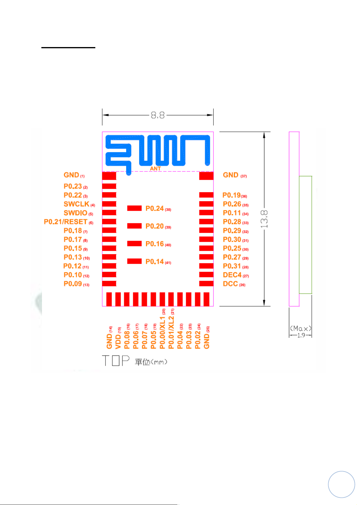
•MDBT42-P
PCB SIZE: (L) 13.8 x (W) 8.8 x (H) 1.9 mm
7
Page 8

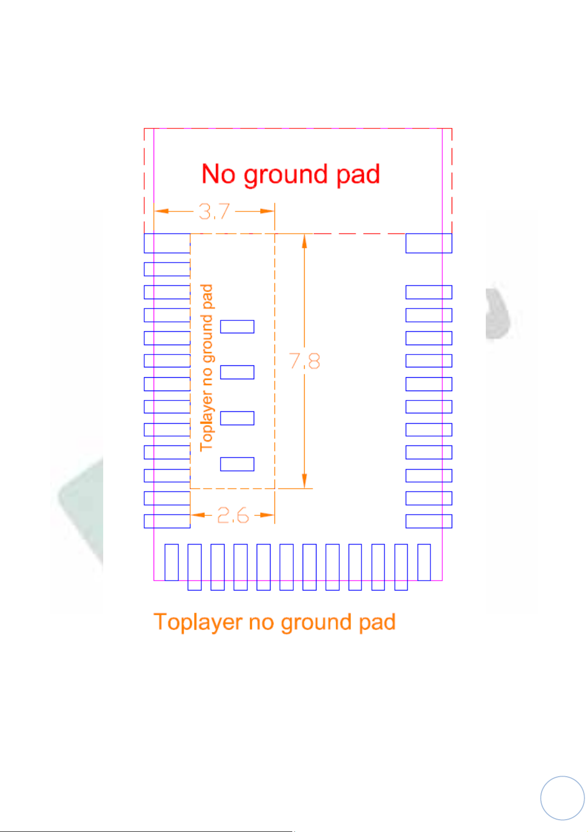
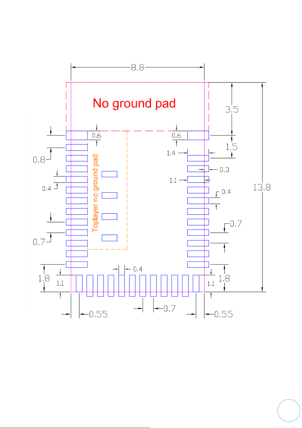
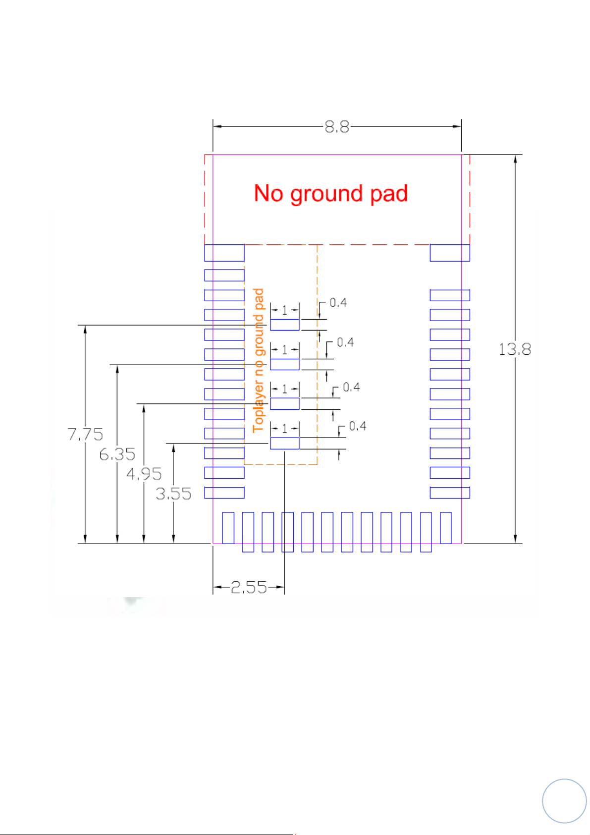
2.2. Recommended Layout of Solder Pad
Graphs are all in Top View, Unit in mm.
8
Page 9
9
Page 10
10
Page 11
11
Page 12
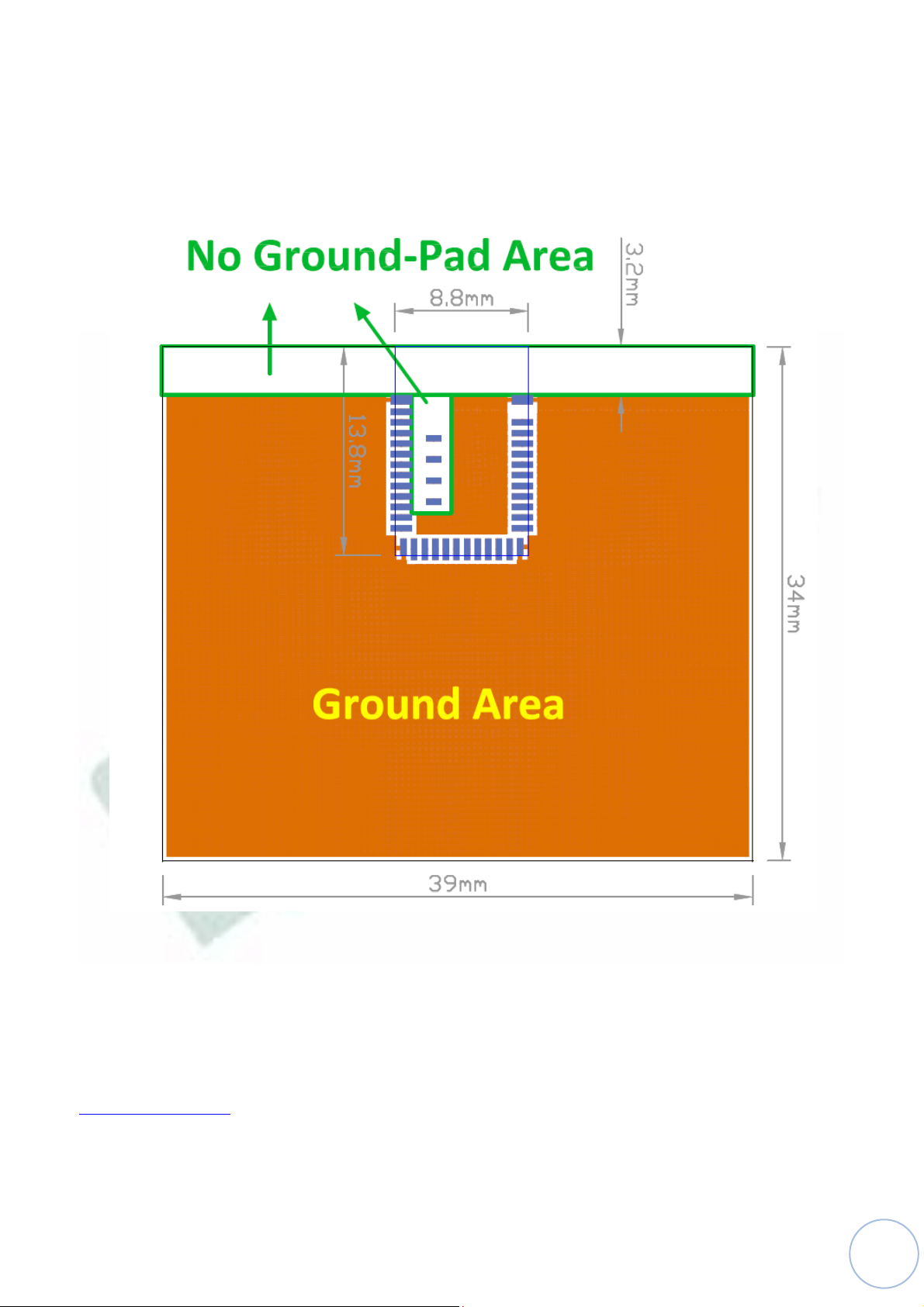
2.3. RF Layout Suggestion (aka Keep-Out Area)
Layout is suggested following below instruction to have better wireless performance. When
design is not allowed to leave such space, please make sure to keep the “No-Ground-Pad” as
wider as it can.
2.4. Footprint & Design Guide
Click to download.
12
Page 13
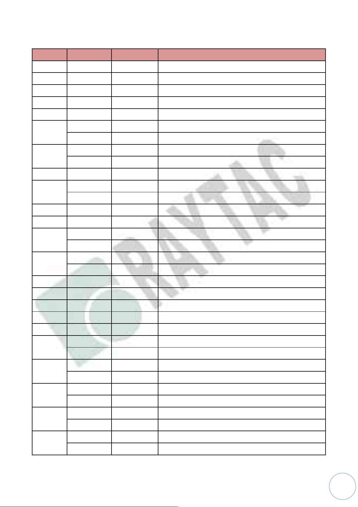
2.5. Pin Assignment
Pin No. Name Pin function Description
(1) GND Ground The pad must be connected to a solid ground plane
(2) P0.23 Digital I/O General-purpose digital I/O
(3) P0.22 Digital I/O General-purpose digital I/O
(4) SWDCLK Digital input Serial Wire debug clock input for debug and programming
(5) SWDIO Digital I/O Serial Wire debug I/O for debug and programming
(6)
(7)
(8) P0.17 Digital I/O General-purpose digital I/O
(9)
(10) P0.13 Digital I/O General-purpose digital I/O
(11) P0.12 Digital I/O General-purpose digital I/O
(12)
(13)
(14) GND Ground The pad must be connected to a solid ground plane
(15) VDD Power Power-supply pin
P0.21 Digital I/O General-purpose digital I/O
RESET Configurable as sy stem RESET pin
P0.18 Digital I/O General-purpose digital I/O
TraceData(0) Tra ce po rt output
P0.15 Digital I/O General-purpose digital I/O
TraceData(2) Tra ce po rt output
P0.10 Digital I/O General-purpose digital I/O
NFC2 NFC input NFC antenna conn ection
P0.09 Digital I/O General-purpose digital I/O
NFC1 NFC input NFC antenna conn ection
(16) P0.08 Digital I/O General-purpose digital I/O
(17) P0.06 Digital I/O General-purpose digital I/O
(18) P0.07 Digital I/O General-purpose digital I/O
(19)
(20)
(21)
(22)
(23)
P0.05 Digital I/O General-purpose digital I/O
AIN3 Analog input SAADC/COMP/LPCOMP input
P0.00 Digital I/O General-purpose digital I/O
XL1 Analog input Connection to 32.768khz crystal (LFXO)
P0.01 Digital I/O General-purpose digital I/O
XL2 Analog input Connection to 32.768khz crystal (LFXO)
P0.04 Digital I/O General-purpose digital I/O
AIN2 Analog input SAADC/COMP/LPCOMP input
P0.03 Digital I/O General-purpose digital I/O
AIN1 Analog input SAADC/COMP/LPCOMP input
13
Page 14
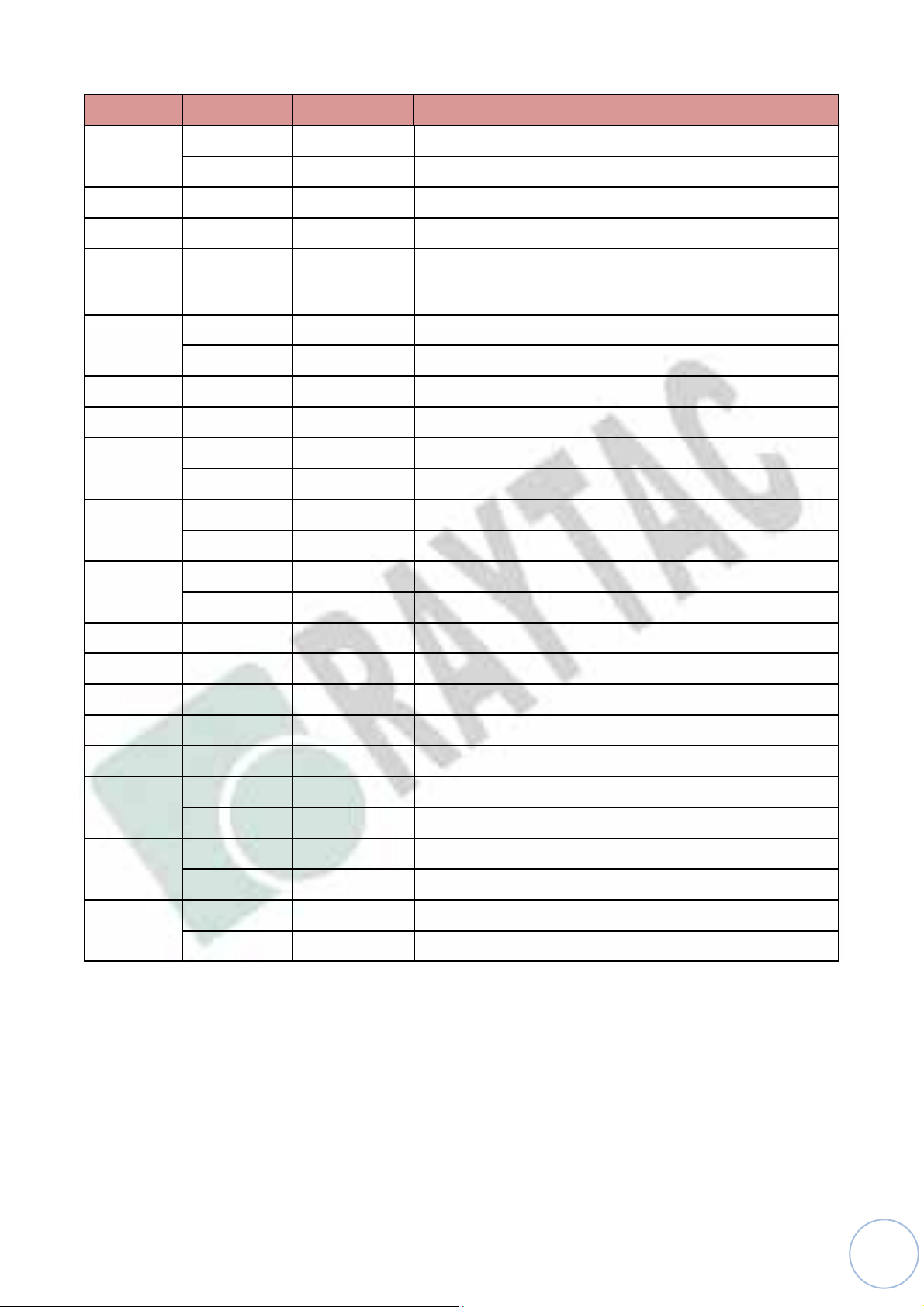
Pin No. Name Pin function Description
(24)
(25) GND Ground The pad must be connected to a solid ground plane
(26) DCC Power DC/DC converter output pin
(27) DEC4 Power
(28)
(29) P0.27 Digital I/O General-purpose digital I/O
(30) P0.25 Digital I/O General-purpose digital I/O
(31)
(32)
(33)
P0.02 Digital I/O General-purpose digital I/O
AIN0 Analog input SAADC/COMP/LPCOMP input
1V3 regulator supply decoupling.
Input from DC/DC converter.
P0.31 Digital I/O General-purpose digital I/O
AIN7 Analog input SAADC/COMP/LPCOMP input
P0.30 Digital I/O General-purpose digital I/O
AIN6 Analog input SAADC/COMP/LPCOMP input
P0.29 Digital I/O General-purpose digital I/O
AIN5 Analog input SAADC/COMP/LPCOMP input
P0.28 Digital I/O General-purpose digital I/O
AIN4 Analog input SAADC/COMP/LPCOMP input
(34) P0.11 Digital I/O General-purpose digital I/O
(35) P0.26 Digital I/O General-purpose digital I/O
(36) P0.19 Digital I/O General-purpose digital I/O
(37) GND Ground The pad must be connected to a solid ground plane
(38) P0.24 Digital I/O General-purpose digital I/O
(39)
(40)
(41)
P0.20 Digital I/O General-purpose digital I/O
TraceCLK Trace port clock output
P0.16 Digital I/O General-purpose digital I/O
TraceData(1) Trace port output
P0.14 Digital I/O General-purpose digital I/O
TraceData(3) Trace port output
14
Page 15
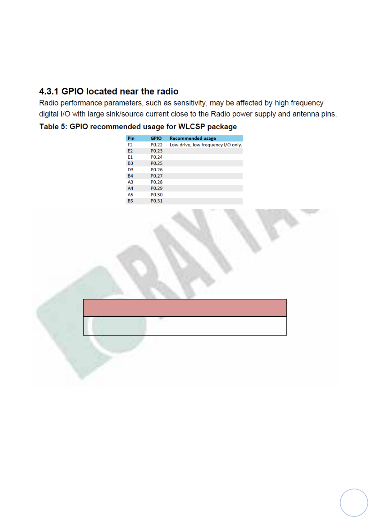
2.6. GPIO Located Near the Radio
Below remarks are extracted from Nordic’s nRF52832 Spec. Any updates shall refer to
Nordic’s official release as final reference.
3. Main Chip Solution
RF IC Crystal Frequency
Nordic NRF52832 32MHZ
15
Page 16
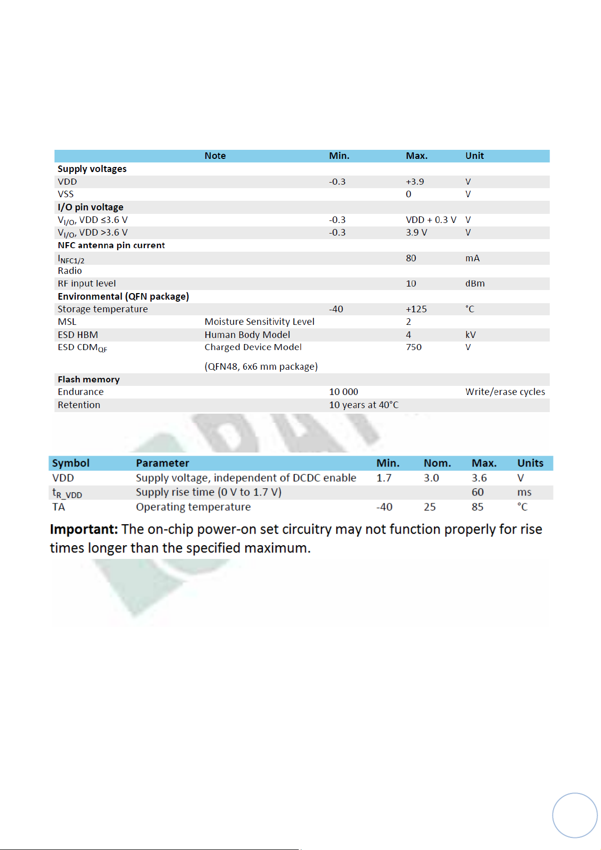
4. Specification
Any technical spec shall refer to Nordic’s official documents as final reference.
4.1. Absolute Maximum Ratings
4.2. Operation Conditions
16
Page 17
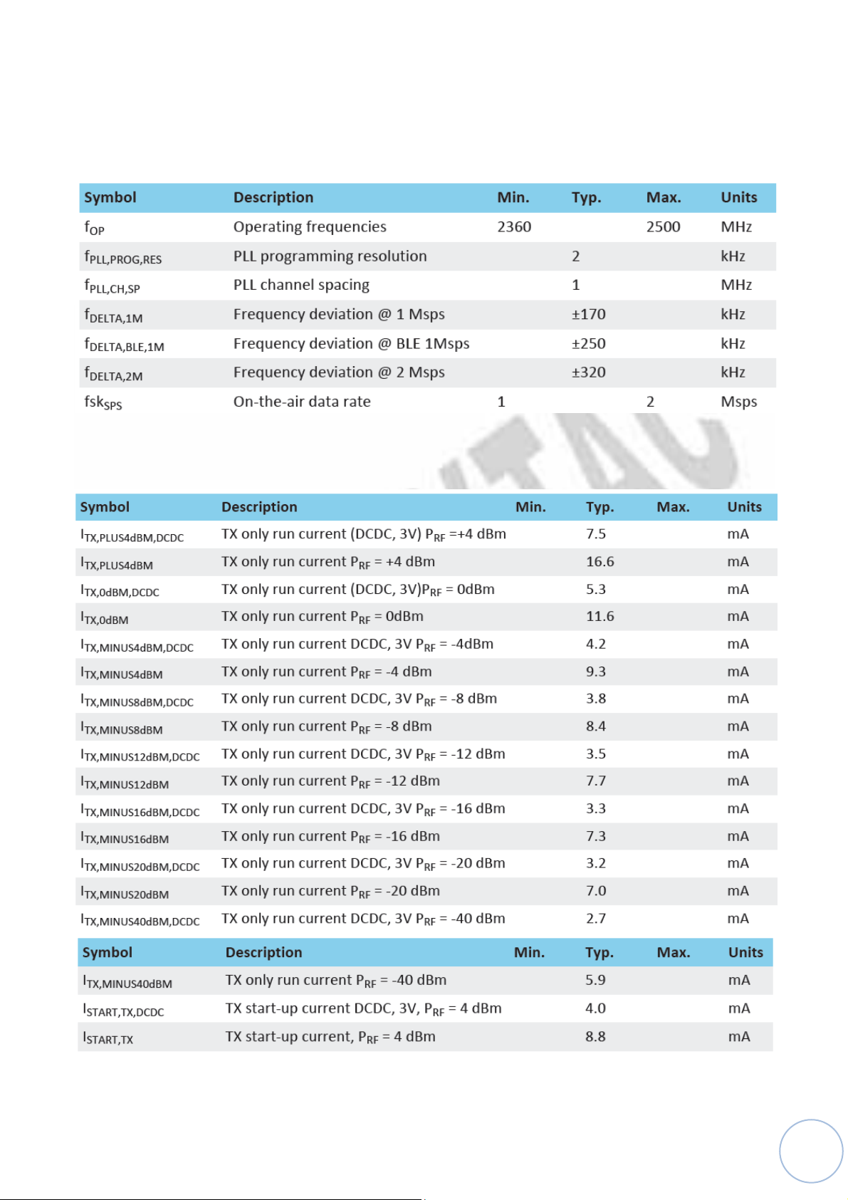
4.3. Electrical Specifications
4.3.1. General Radio Characteristics
4.3.2. Radio Current Consumption (Transmitter)
17
Page 18
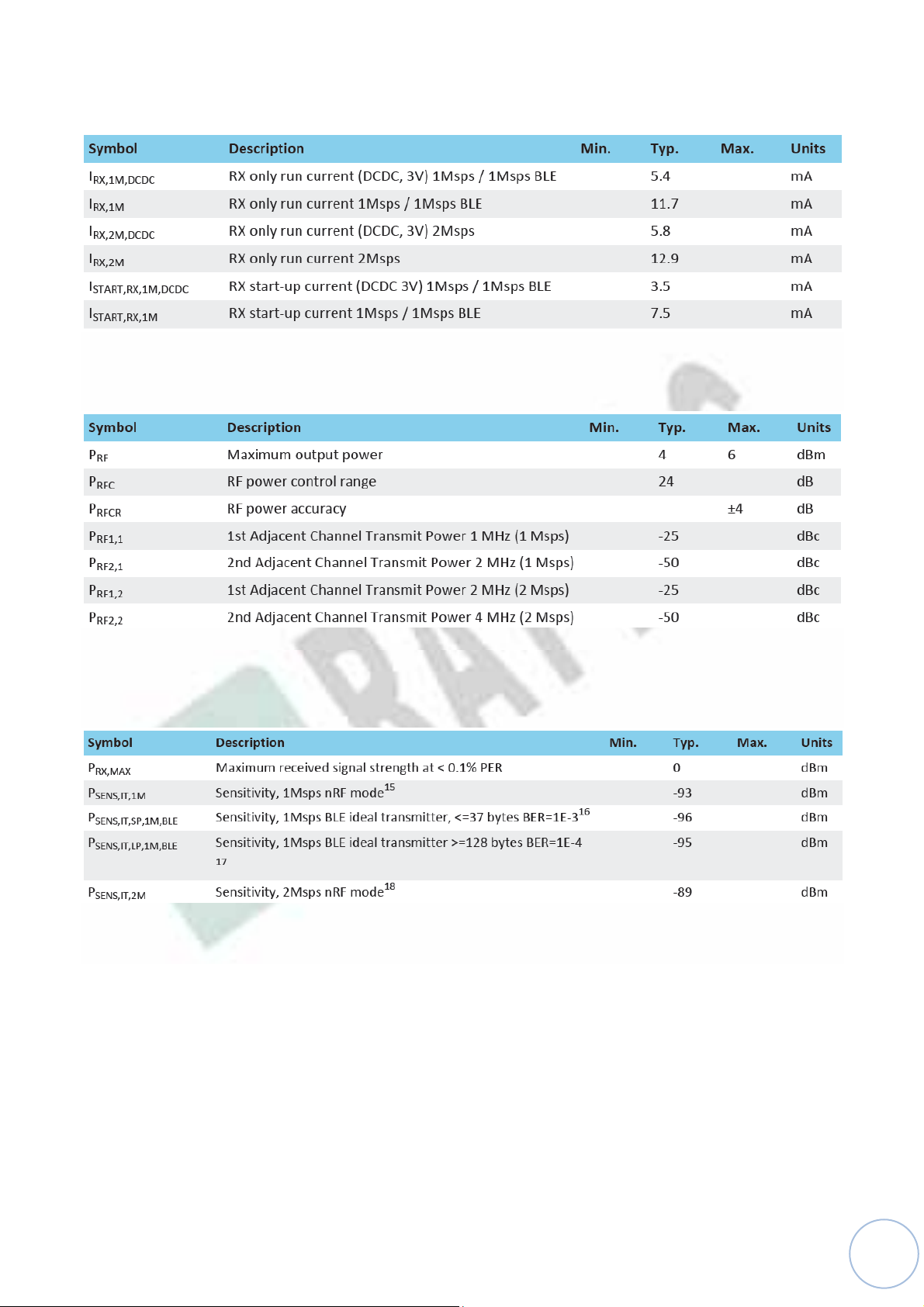
4.3.3. Radio Current Consumption (Receiver)
4.3.4. Transmitter Specification
4.3.5. Receiver Operation
18
Page 19
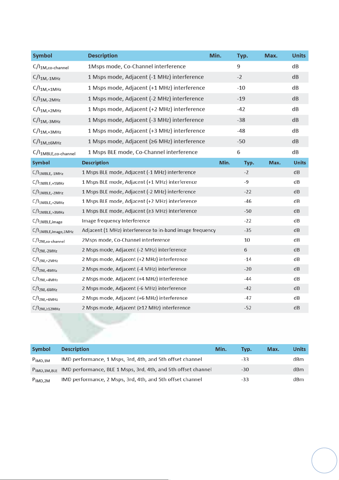
4.3.6. RX Selectivity
4.3.7. RX Intermodulation
19
Page 20
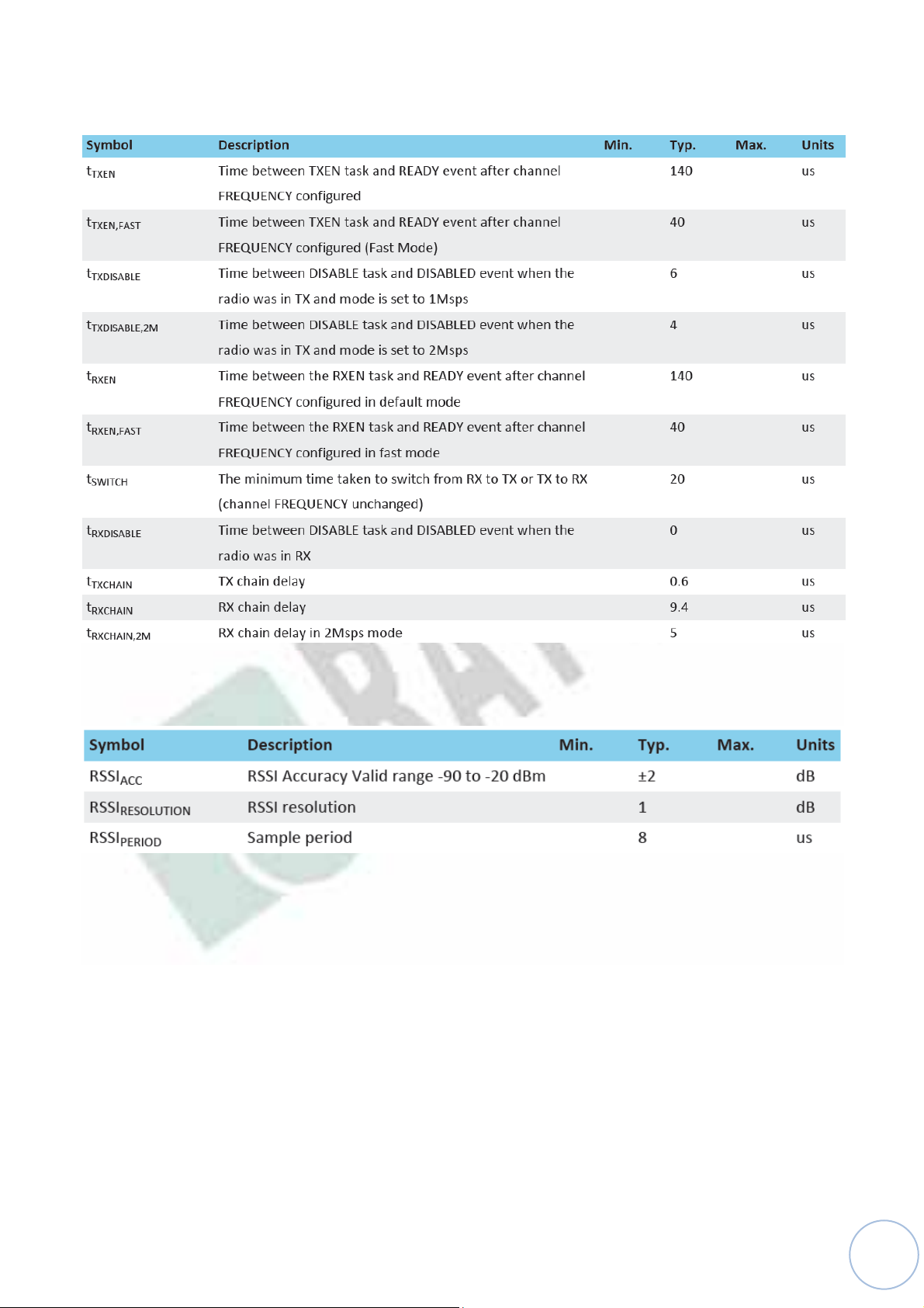
4.3.8. Radio Timing Parameters
4.3.9. RSSI Specifications
20
Page 21
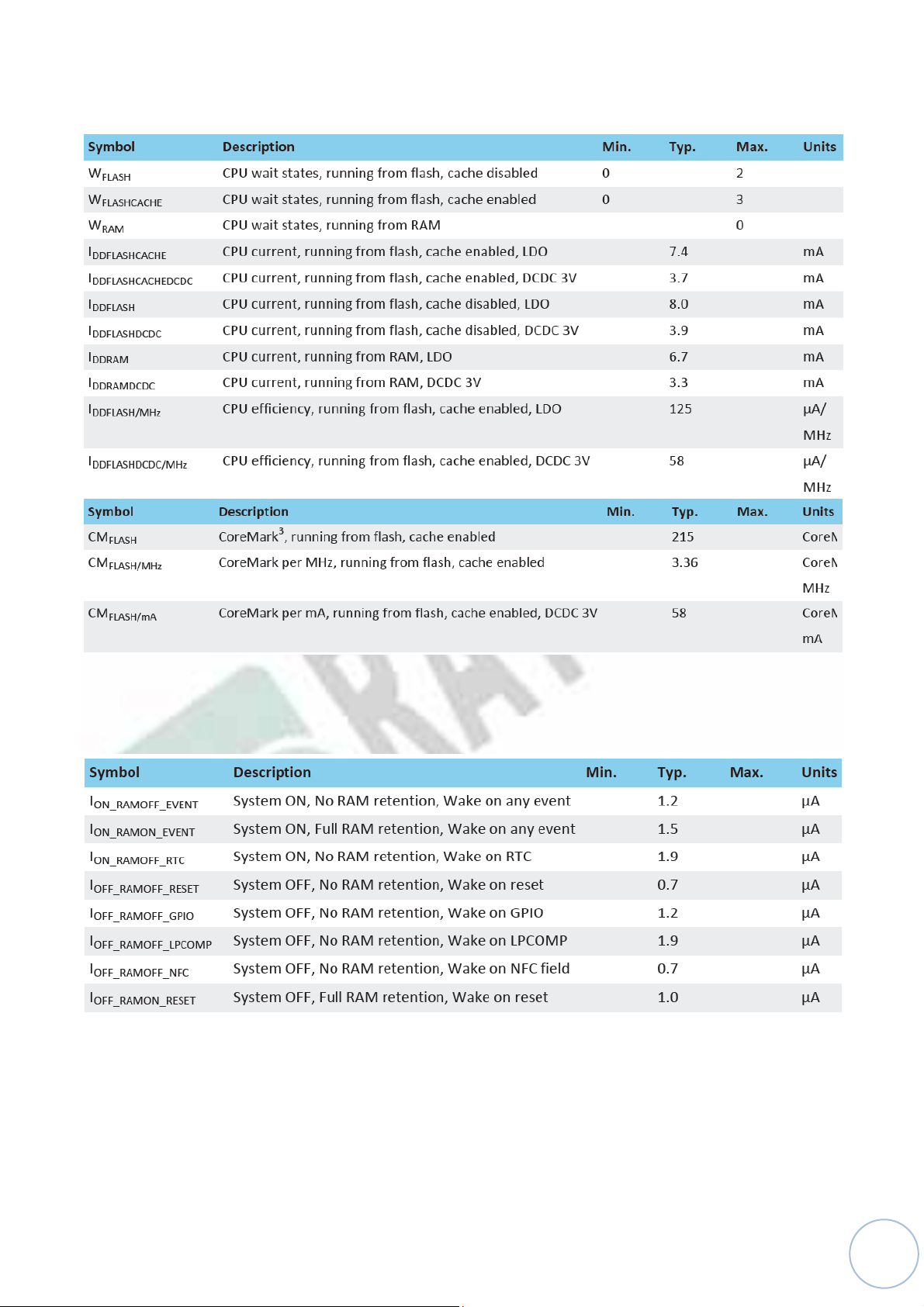
4.3.10. CPU
4.3.11. Power Management
21
Page 22

5. FCC Compliance
This equipment has been tested and found to comply with the limits for a Class digital device,
pursuant to Part 15 of the FCC rules. These limits are designed to provide reasonable
protection against harmful interference in a residential installation. This equipment generates
uses and can radiate radio frequency energy and, if not installed and used in accordance with
the instructions, may cause harmful interference to the radio communications. However, there
are no guarantees that interference will not occur in a particular installation.
Troubleshooting
If this equipment does cause harmful interference to radio reception, which can be
determined by turning the equipment off and on, the user is encouraged to correct the
interference by one or more of the following instructions.
.Reorient or relocate the receiving antenna.
.Increase the separation between the equipment and receiver.
.Consult dealer or an experienced radio technician.
Conditions
Operation is subject to the following conditions
.This device may not cause harmful interference.
.This device must accept any interference received, including interference that may
cause undesired operation.
FCC Caution
This device complies with Part 15 of the FCC rules. Operation is subject to the following two
conditions: (1) this device may not cause harmful interference, and (2) this device must
accept any interference received, including interference that may cause undesired operation.
Any changes or modifications not expressly approved by the party responsible for compliance
could void the authority to operate equipment.
RF Exposure
For body worn operation, this device has been tested and meets FCC RF exposure
guidelines when used with an accessory that contains no metal and that positions the
handset a minimum of 5mm from the body. Use of other accessories may not ensure
compliance with FCC RF exposure guidelines.
End Product Labeling
This transmitter module is authorized only for use in device where the antenna may be
installed such that 5mm may be maintained between the antenna and users. The final end
22
Page 23

product must be labeled in a visible area with the following:
Contains FCC ID: SH6MDBT42
Manual Information to the End User
The OEM integrator has to be aware not to provide information to the end user regarding how
to install or remove this RF module in the user’s manual of the end product which integrates
this module. The end user manual shall include all required regulatory information/warming
as shown in this manual.
23
Page 24

6. IC Caution
This device complies with Industry Canada licence-exempt RSS standard(s). Operation is
subject to the following two conditions:
.This device may not cause interference
.This device must accept any interference, including interference that may cause undesired
operation of the device
RF exposure
To comply with the FCC RF exposure compliance requirements, this device and its antenna
must not be co-located or operating in conjunction with any other antenna or transmitter.
Le présent appareil est conforme aux CNR d'Industrie Canada applicables aux appareils
radio exempts de licence.L'exploitation est autorisée aux deux conditions suivantes:
.l'appareil ne doit pas produire de brouillage, et
.l'utilisateur de l'appareil doit accepter tout brouillage radioélectrique subi, même si le
brouillage est susceptible d'en compromettre le fonctionnement.
Pour se conformer aux exigences de conformité RF canadienne l'exposition, cet appareil et
son antenne ne doivent pas être co-localisés ou fonctionnant en conjonction avec une autre
antenne
ou transmetteur.
End Product Labeling
This transmitter module is authorized only for use in device where the antenna may be
installed such that 5mm may be maintained between the antenna and users. The final end
product must be labeled in a visible area with the following:
Contains IC ID: 8017A-MDBT42
24
Page 25

7. NCC 警語
根據 NCC 低功率電波輻射性電機管理辦法規定
第十二條:
經型式認證合格之低功率射頻電機,非經許可,公司、商號或使用者均不得擅自變更頻率、加
大功率或變更原設計之特性及功能。
第十四條:
低功率射頻電機之使用不得影響飛航安全及干擾合法通信;經發現有干擾現象時,應立即停用,
並改善至無干擾時方得繼續使用。前項合法通信,指依電信法規定作業之無線電通信。
低功率射頻電機須忍受合法通信或工業、科學及醫療用電波輻射性電機設備之干擾。
此模組於取得認證後將依規定於模組本體標示審驗合格標籤,並要求平台廠商於平台上標示。
「本產品內含射頻模組:ID 編號 XXXXX」字樣
25
 Loading...