

Page 1
Rayson
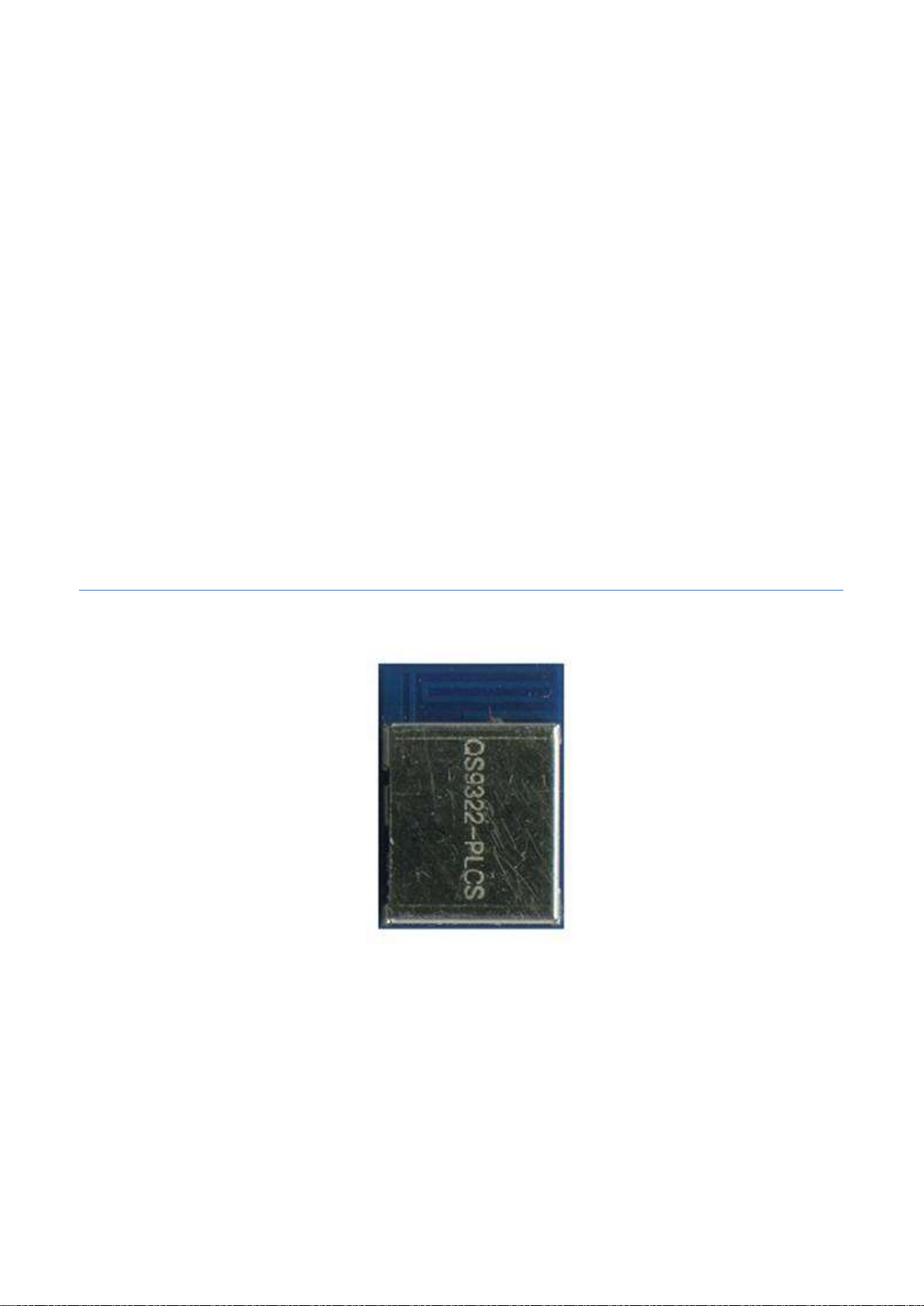
QS9322 Bluetooth 4.0 Low Energy Module
Datasheet
Version 2.0
Rev1.9 (8/28) Confidential and Proprietary ©2012-2014 by Rayson.
Confidential A Confidential Information contained herein is covered under Non-Disclosure Agreement (NDA).
Preliminary datasheet, Rayson reserves right to modify without notification
Page 2

VERSION HISTORY
Version Comment
1.0 First release
1.1 Add the photo of QS9322 with shielding box
1.2 Change transparent transfer baud rate to 115200. Connect Pin19 to Vin in figure 1 and 7.
1.3 Add CE note
1.4 Add model definition, Layout Guide instruction and Soldering Recommendations
1.8 Add CE and FCC qualification information
1.9 Change the pin19 description. Power supply (2.4~3.6V)
2.0 Update CE and FCC qualification information
Rev2.0 (7/28) Confidential and Proprietary ©2012-2014 by Rayson Corporation, not for distribution.
Confidential A Confidential Information contained herein is covered under Non-Disclosure Agreement (NDA).
Preliminary datasheet, Rayson Corporation reserves right to modify without notification
Page 3

Table of Contents
1 Key Features ............................................................................................................................................... 1
2 Description .................................................................................................................................................. 3
2.1 Model Definition ................................................................................................................................. 3
2.2 Module description .............................................................................................................................. 3
3 Pin out ......................................................................................................................................................... 4
4 Electrical Characteristics ............................................................................................................................ 6
5 Layout and Physical Dimensions ................................................................................................................ 7
5.1 Physical dimensions ............................................................................................................................ 7
5.2 Layout guide ........................................................................................................................................ 7
6 Soldering Recommendations ...................................................................................................................... 9
7 Application Reference .............................................................................................................................. 10
Rev2.0 (7/28) Confidential and Proprietary ©2012-2014 by Rayson Corporation, not for distribution.
Confidential A Confidential Information contained herein is covered under Non-Disclosure Agreement (NDA).
Preliminary datasheet, Rayson Corporation reserves right to modify without notification
Page 4

1 Key Features
Bluetooth® 4.0 Low Energy wireless module
Frequency bands: 2400MHz to 2483.5MHhz
1Mbps on air data rate
Slave and Master mode operation
Support up to 8 simultaneous links in master mode
128-bit AES coprocessor
Complete BLE protocol stack and application profiles
Integrated 32-bit Cortex-M0 MCU with
64KB system memory
128KB flash
Ultra Low Power Consumption
2uA deep sleep mode
3uA sleep mode (32kHz RC OSC on)
DC-DC mode
9.25mA RX current at 3V
8.8mA TX current @0dBm Tx power at 3V
Non DC-DC mode
13.6mA RX current at 3V
13.3mA TX current @0dBm Tx power at 3V
Integrated DC-DC converter and LDO
3V DC power supply or DC 3V coin cell
High Performance
-95dBm RX sensitivity (Non DC-DC mode)
-93dBm RX sensitivity (DC-DC mode)
Tx power from -20dBm to 4dBm
Excellent link budget up to 99dB
Complete Protocol Stack and Profile
Bluetooth® v4.0
Bluetooth® v4.0 host stack including L2CAP , SMP, ATT, GATT, GAP
Qualified application profiles and services
Controller subsystem QDID: B021031
Host stack subsystem QDID: B021098
Profile subsystem QDID: B021946
Rev2.0 (7/28) Confidential and Proprietary ©2012-2014 by Rayson Corporation, not for distribution. Page 1 of 13
Confidential A Confidential Information contained herein is covered under Non-Disclosure Agreement (NDA).
Preliminary datasheet, Rayson Corporation reserves right to modify without notification
Page 5

Certifications
Bluetooth EPL
RoHS qualified
CE qualified
Modular certification for FCC
Ease of Design
Small form factor: QS9322-PLCS, 9x13x2.2mm;
Easy to use command set over UART/SPI to communicate with App MCU
PCB antenna with impedance matching
Application
Sports & Fitness
Healthcare & Wellness
Remote Control
PC Peripherals (mouse, keyboard)
Mobile Phone Accessories
Home/building Automation
Industrial automation
Wireless Sensor Networks
Rev2.0 (7/28) Confidential and Proprietary ©2012-2014 by Rayson Corporation, not for distribution. Page 2 of 13
Confidential A Confidential Information contained herein is covered under Non-Disclosure Agreement (NDA).
Preliminary datasheet, Rayson Corporation reserves right to modify without notification
Page 6

2 Description
2.1 Model Definition
QS9322-PLCS
FCC ID: QWO-QS9322PLCS.
IC ID : 4460A-QS9322PLCS
2.2 Module description
QS9322 is a compact, surface mount Bluetooth 4.0 Low Energy (BLE) compliant wireless module. It
integrates an advanced single-chip BLE SoC chip – QN9021 with RF circuit and PCB antenna in a compact
module. Embedded 16 MHz and 32.678 kHz crystals are used for clock generation. Impedance matching
provides optimal radio performance with extremely low spurious emissions. QS9322 can be used directly
with a coin cell battery or 3V DC regulated DC power supply.
Small size gives good radiation efficiency with low price even when the module is used in layouts with
very limited space and easy modular handling.
QS9322 offers all Bluetooth low energy features: radio, stack, profiles and application space for
customer applications, so no external processor is needed. QS9322 can also be used to transfer raw data
between each other through the factory built-in application.
The pre-qualified module enables users to add Bluetooth Low Energy to traditional products within the
shortest time. QS9322 is leading the way for the new generation of Bluetooth low energy modules.
Rev2.0 (7/28) Confidential and Proprietary ©2012-2014 by Rayson Corporation, not for distribution. Page 3 of 13
Confidential A Confidential Information contained herein is covered under Non-Disclosure Agreement (NDA).
Preliminary datasheet, Rayson Corporation reserves right to modify without notification
Page 7

3 Pin out
U4
Table 1 Pin out description
PIN
NAME FUNCTION DESCRIPTION
25
24
23
22
21
20
19
18
GND
GND
GND
GND
P3.1_ADC+
P3.0_ADCVDD_IDC
GND
SWCLK16XTAL_32K_IN14P0.3_IN T0
EXT_VCC
17
SWDI O
15
13
P2.3_I2C -SDA
P1.0_SPI1-MISO
P1.1_SPI1-MOSI
P1.3_SPI1-C LK
P0.0_UAR T0-T X11P1.7_UAR T0-R X
XTAL_32K_OUT
12
GND
/RSTN
P2.4_I2C -SCL
P1.2_SPI1-C S
GND
10
Figure 1 PCB Antenna pin out
1
2
3
4
5
6
7
8
9
1 GND Ground Should be connected to ground plane on application PCB
2 /RSTN Digital Input Hardware reset, active low.
3 P2.3/SDA Digital in/out GPIO / I2C data with pull-up
4 P2.4/SCL Digital in/out GPIO / I2C clock
5 P1.0/SPI_MISO Digital in/out GPIO / SPI data master in/slave out
6 P1.1/SPI_MOSI Digital in/out GPIO / SPI data master out/slave in
7 P1.2/SPI_CS Digital in/out GPIO / SPI chip select
8 P1.3/SPI_CLK Digital in/out GPIO / SPI clock
9 GND Ground Should be connected to ground plane on application PCB
10 P1.7/UART_RX
Digital input
GPIO / UART RX data input
11 P0.0/UART_TX Digital output GPIO / UART TX data output
12 P0.3/INT0 Digital in GPIO / Interrupt
13 32K_CLOCK1 Analog in Not connected
14 32K_CLOCK2 Analog out Not connected
15 SWDIO Digital in/out SWD data with pull-up
16 SWCLK Digital in SWD clock input with pull-up
17 VCC Power Power supply (2.4~3.6V)
18 GND Ground Should be connected to ground plane on application PCB
19 VDD_IDC Power Power supply (2.4~3.6V)
Rev2.0 (7/28) Confidential and Proprietary ©2012-2014 by Rayson Corporation, not for distribution. Page 4 of 13
Confidential A Confidential Information contained herein is covered under Non-Disclosure Agreement (NDA).
Preliminary datasheet, Rayson Corporation reserves right to modify without notification
Page 8

20 P3.0/ADC- Analog in GPIO / ADC-
21 P3.1/ADC+ Analog in GPIO / ADC+
22 GND Ground Should be connected to ground plane on application PCB
23 GND Ground Should be connected to ground plane on application PCB
24 GND Ground Should be connected to ground plane on application PCB
25 GND Ground Should be connected to ground plane on application PCB
Rev2.0 (7/28) Confidential and Proprietary ©2012-2014 by Rayson Corporation, not for distribution. Page 5 of 13
Confidential A Confidential Information contained herein is covered under Non-Disclosure Agreement (NDA).
Preliminary datasheet, Rayson Corporation reserves right to modify without notification
Page 9

4 Electrical Characteristics
Table 2 Recommended Operating Conditions
SYMBOL PARAMETER CONDITIONS MIN TYP MAX UNIT
VCC Power supply Relative to GND 2.4 3.0 3.6 V
TA Operating temperature -40 +25 +85 ℃
Table 3 Current Consumption
SYMBOL CONDITIONS MIN TYP MAX UNIT
Icc Deep sleep mode 2 uA
Sleep mode 3 uA
Idle mode (w/o DC-DC) 0.84 mA
MCU @8MHz (w/o DC-DC) 1.35 mA
RX mode(w/o DC-DC) 13.6 mA
RX mode (w/t DC-DC) 9.25 mA
TX mode @0dBm Txpower (w/o DC-DC) 13.3 mA
TX mode @0dBm Txpower ( w/t DC-DC) 8.8 mA
(Typical values are TA = 25℃ and VCC =3V)
Notes:
1. Current Consumption includes analog and digital.
2. Depend on IO conditions.
3. Deep sleep mode: digital regulator off, no clocks, POR, RAM/register content retained
4. Sleep mode: digital regulator off, 32k RC OSC on, POR, sleep timer on, and RAM/register content retained
5. Idle: 16MHz OSC on, no radio or peripherals, 8 MHz system clock and MCU idle (no code execution)
6. MCU@8 MHz: MCU running at 8 MkHz RC OSC clock, no radio or peripherals
7. RX sensitivity is -95dBm sensitivity when DC-DC is disabled.
8. RX sensitivity is -93dBm sensitivity when DC-DC is enabled.
Rev2.0 (7/28) Confidential and Proprietary ©2012-2014 by Rayson Corporation, not for distribution. Page 6 of 13
Confidential A Confidential Information contained herein is covered under Non-Disclosure Agreement (NDA).
Preliminary datasheet, Rayson Corporation reserves right to modify without notification
Page 10

5 Layout and Physical Dimensions
5.1 Physical dimensions
Figure 2 Physical dimensions and pinout (mm) – Top view
5.2 Layout guide
For optimal performance of the antenna place the module at the position of the PCB as shown in the
following figures. Do not place any metal (traces, components, battery etc.) within the clearance area of
the antenna. Connect all the GND pins directly to a solid GND plane. Place the GND vias as close to the GND
pins as possible. Use good layout practices to avoid any excessive noise coupling to signal lines or supply
voltage lines.
Place nothing around the antenna for the high antenna performance as shown in Figure 3. If can’t
layout as aforesaid, avoid placing GND plane closer than 5 mm as shown in Figure 4 and any other dielectric
material closer than 1 mm from the antenna as shown in Figure 5. Anything closer than this distance from
the antenna will detune the antenna to lower frequencies and reduce the RF power.
Figure 3 Layout for high performance
Rev2.0 (7/28) Confidential and Proprietary ©2012-2014 by Rayson Corporation, not for distribution. Page 7 of 13
Confidential A Confidential Information contained herein is covered under Non-Disclosure Agreement (NDA).
Preliminary datasheet, Rayson Corporation reserves right to modify without notification
Page 11

Figure 4 Layout when GND plane around antenna
Figure 5 Layout when any dielectric material around antenna
Rev2.0 (7/28) Confidential and Proprietary ©2012-2014 by Rayson Corporation, not for distribution. Page 8 of 13
Confidential A Confidential Information contained herein is covered under Non-Disclosure Agreement (NDA).
Preliminary datasheet, Rayson Corporation reserves right to modify without notification
Page 12

6 Soldering Recommendations
QS9322 is compatible with industrial standard reflow profile for Pb-free solders. The reflow profile used is
dependent on the thermal mass of the entire populated PCB, heat transfer efficiency of the oven and
particular type of solder paste used. Consult the datasheet of particular solder paste for profile
configurations.. Since the profile used is process and layout dependent, the optimum profile should be
studied case by case. Thus following recommendation should be taken as a starting point guide.
- Refer to technical documentations of particular solder paste for profile configurations
- Avoid using more than one flow.
- Aperture size of the stencil should be 1:1 with the pad size.
Rev2.0 (7/28) Confidential and Proprietary ©2012-2014 by Rayson Corporation, not for distribution. Page 9 of 13
Confidential A Confidential Information contained herein is covered under Non-Disclosure Agreement (NDA).
Preliminary datasheet, Rayson Corporation reserves right to modify without notification
Page 13

7 Application Reference
QS9322 integrates BLE SoC chip – QN9021 with RF circuit and PCB antenna in a compact module. It can
be used directly with a coin cell battery or 3V DC regulated power supply.
QS9322 can be used as a MCU with BLE feature, and also be used as a RF module to transfer raw data
between each other through the factory built-in application.
When QS9322 is used as a MCU with BLE feature, program flow can refer to the QN902x’s user manual.
When QS9322 is used as only a RF module for transfer raw data, the reference circuit schematic and
programming guide can refer to QS9322 BLE Module User Manual.
Rev2.0 (7/28) Confidential and Proprietary ©2012-2014 by Rayson Corporation, not for distribution. Page 10 of 13
Confidential A Confidential Information contained herein is covered under Non-Disclosure Agreement (NDA).
Preliminary datasheet, Rayson Corporation reserves right to modify without notification
Page 14

Note1:
This device complies with Part 15 of the FCC Rules. Operation is subject to the following two conditions:
(1) this device may not cause harmful interference.
(2) this device must accept any interference received, including interference that may cause undesired operation.
changes or modifications not expressly approved by the party responsible for compliance could void the user’s
authority to operate the equipment.
Please notice that if the FCC identification number is not visible when the module is installed inside another device,
then the outside of the device into which the module is installed must also display a label referring to the enclosed
module. This exterior label can use wording such as the following: “Contains FCC ID: QWO-QS9322PLCS “ any similar
wording that expresses the same meaning may be used.
This equipment complies with FCC radiation exposure limits set forth for an uncontrolled environment. This
equipment should be installed and operated with a minimum distance of 5mm between the radiator & your body.
This transmitter must not be co-located or operating in conjunction with any other antenna or transmitter.
Note2:
This device complies with Industry Canada license-exempt RSS standard(s). Operation is subject to the following two
conditions: (1) this device may not cause interference, and (2) this device must accept any interference, including
interference that may cause undesired operation of the device.
Le présent appareil est conforme aux CNR d'Industrie Canada applicables aux appareils radio exempts de licence.
L'exploitation est autorisée aux deux conditions suivantes : (1) l'appareil ne doit pas produire de brouillage, et (2)
l'utilisateur de l'appareil doit accepter tout brouillage radioélectrique subi, même si le brouillage est susceptible d'en
compromettre le fonctionnement.
Please notice that if the IC identification number is not visible when the module is installed inside another device, then
the outside of the device into which the module is installed must also display a label referring to the enclosed module.
This exterior label can use wording such as the following: “Contains IC: 4460A-QS9322PLCS” any similar wording that
expresses the same meaning may be used.
L’étiquette d’homologation d’un module d’Innovation, Sciences et Développement économique Canada devra être
posée sur le produit hôte à un endroit bien en vue, en tout temps. En l’absence d’étiquette, le produit hôte doit porter
une étiquette sur laquelle figure le numéro d’homologation du module d’Innovation, Sciences et Développement
économique Canada, précédé du mot « contient », ou d’une formulation similaire allant dans le même sens et qui va
comme suit :
Contient IC : 4460A-QS9322PLCS est le numéro d’homologation du module.
Rev2.0 (7/28) Confidential and Proprietary ©2012-2014 by Rayson Corporation, not for distribution. Page 11 of 13
Confidential A Confidential Information contained herein is covered under Non-Disclosure Agreement (NDA).
Preliminary datasheet, Rayson Corporation reserves right to modify without notification
Page 15

Note3:
The module is limited to OEM installation ONLY.
The OEM integrator is responsible for ensuring that the end-user has no manual instruction to remove or
install module.
The module is limited to installation in mobile application;
A separate approval is required for all other operating configurations, including portable configurations with
respect to Part 2.1093 and difference antenna configurations.
There is requirement that the grantee provide guidance to the host manufacturer for compliance with Part
15B requirements.
Rev2.0 (7/28) Confidential and Proprietary ©2012-2014 by Rayson Corporation, not for distribution. Page 12 of 13
Confidential A Confidential Information contained herein is covered under Non-Disclosure Agreement (NDA).
Preliminary datasheet, Rayson Corporation reserves right to modify without notification
Page 16

Rev2.0 (7/28) Confidential and Proprietary ©2012-2014 by Rayson Corporation, not for distribution. Page 13 of 13
Confidential A Confidential Information contained herein is covered under Non-Disclosure Agreement (NDA).
Preliminary datasheet, Rayson Corporation reserves right to modify without notification
 Loading...