

RAMTRON VRS51C540-40-L, VRS51L540-25-L, VRS51C540-40-Q, VRS51L540-25-Q, VRS51C540-40-P DATA SHEET
...
VRS51x540
Datasheet Rev 1.2
Versa 8051 MCU with 4KB Flash
Overview
The VRS51x540 is a low cost 8-bit microcontroller
based on the standard 80C51 microcontroller family
architecture. It is pin compatible and is a drop-in
replacement for standard 8051 MCUs
Aimed at cost effective applications requiring small
amounts of program/data memory coupled with
streamlined peripheral support, the VRS51x540 includes
4KB of Flash memory, 128 bytes of RAM a UART, three
16-bit timers, a Watchdog timer and power down
features.
The VRS51x540 is available in 5 (VRS51C540) and 3.3
(VRS51L540) volt versions in PLCC-44, QFP-44 and
DIP-40 packages. The VRS51x540 devices operate
over the entire industrial temperature range. The Flash
memory can be programmed using programmers
available from Ramtron or other 3rd party commercial
programmers.
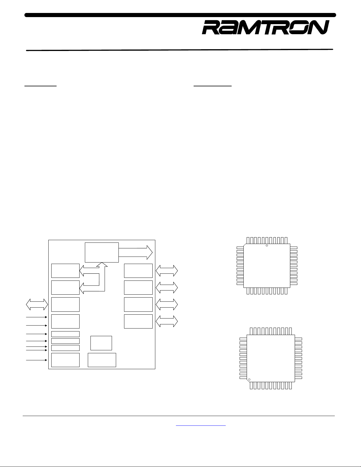
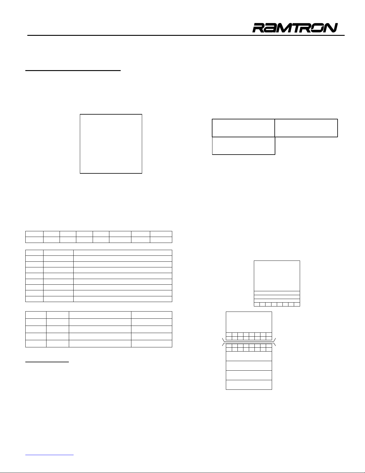
FIGURE 1: VRS51X540 FUNCTIONAL DIAGRAM
4KB
FLASH
128 Bytes of
RAM
UART
8051
PROCESSOR
ADDRESS/
DATA BUS
PORT 0
PORT 1
PORT 2
8
8
8
Feature Set
• 80C51/80C52 pin compatible
• 12 clock periods per machine cycle
• 4KB on-chip Flash memory
• 128 bytes on-chip data RAM
• 32 I/O lines: P0-P3 = 8-bit
• Full duplex serial port (UART)
• 3, 16-bit Timers/Counters
• Watchdog Timer
• 8-bit Unsigned Division / Multiply
• BCD arithmetic
• Direct and Indirect Addressing
• Two levels of interrupt priority and nested interrupts
• Power saving modes
• Code protection function
• Operates at a clock frequency of up to 40MHz
• Low EMI (inhibit ALE)
• Programming voltage: 12V
• Industrial Temperature range (-40°C to +85°C)
• 5V and 3V versions available (see ordering information.)
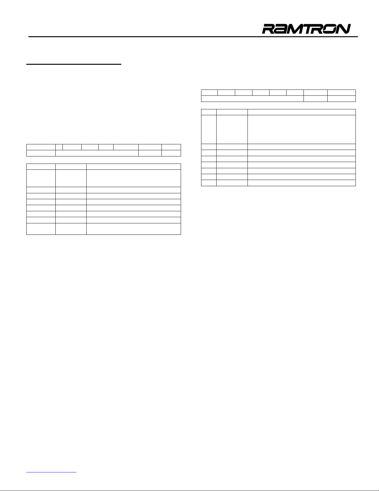
FIGURE 2: VRS51X540 PLCC AND QFP PINOUT DIAGRAMS
3
1
D
D
A
A
/
/
3
1
.
.
0
NC
T2/P1.0
1
S
C
S
N
V
0
P0.0/AD0
VDD
P0.2/AD2
P
P
40
39
P0.4 /AD4
P0.5 /AD5
P0.6 /AD6
P0.7 /AD7
#EA
NC
ALE
#PSEN
P2.7 /A15
P2.6 /A14
P2.5 /A13
29
28
1
2
1
1
A
A
/
/
3
4
.
.
2
2
P2.1/A9
P2.0/A8
P
P2.2/A10
P
P1.5
P1.6
P1.7
RESET
RXD/P3.0
TXD/P3.1
#INT0/P 3.2
#INT1/P 3.3
T0/P 3.4
T1/P 3.5
3
2
.
.
1
1
P
P1.4
T2EX/P1.1
P
6
7
17
18
6
.
3
P
/
R
W
#RD/P3.7
#
VRS51x540
PLCC-44
1
2
L
L
A
A
T
T
X
X
NC
2 INTERRUPT
INPUTS
TIMER 0
TIMER 1
TIMER 2
RESET
POWER
CONTROL
WATCHDOG
TIMER
PORT 3
8
P0.3/AD3
P0.2/AD2
P0.1/AD1
P0.0/AD0
VDD
NC
T2/P1.0
T2EX/P1.1
P1.2
P1.3
P1.4
P0.7/AD7
#EA
P0.5/AD5
P0.6/AD6
P0.4/AD4
3
3
3
4
VRS51x540
QFP-44
4
4 1
1
P1.6
P1.5
P1.7
RESET
RXD/P3.0
P2.6/A14
P2.5/A13
#PSEN
P2.7/A15NCALE
2
2
3
P2.4/A12
2
P2.3/A11
P2.2/A10
P2.1/A9
P2.0/A8
NC
VSS
XTAL1
XTAL2
#RD/P3.7
1
#WR/P3.6
2
1
NC
T0/P3.4
T1/P3.5
TXD/P3.1
#INT0/P3.2
#INT1/P3.3
Ramtron International Corporation
1850 Ramtron Drive Colorado Springs
Colorado, USA, 80921
http://www.ramtron.com
?
MCU customer service: 1-800-943-4625, 1-514-871-2447, ext. 208
?
1-800-545-FRAM, 1-719-481-7000
?
page 1 of 40
VRS51x540
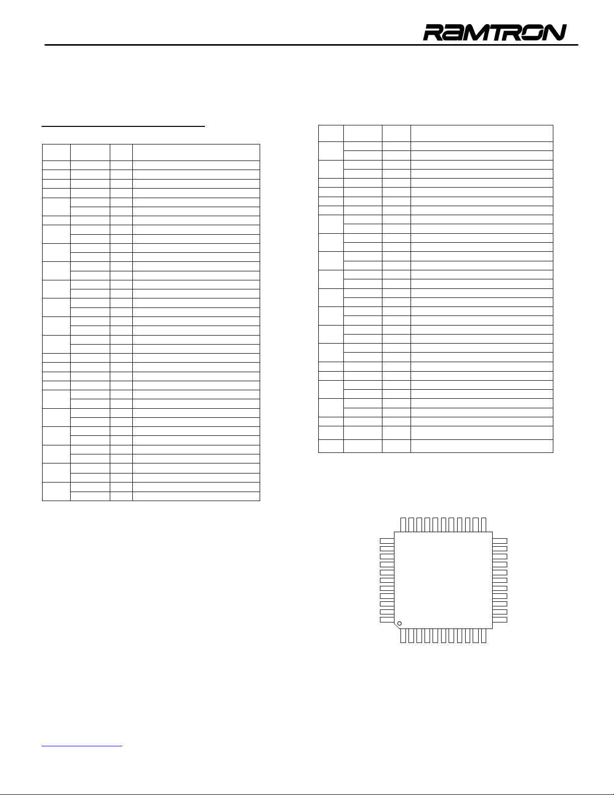
Pin Descriptions for QFP-44
TABLE 1: PIN DESCRIPTIONS FOR QFP-44/
QFP
Name I/O Function
- 44
1 P1.5 I/O Bit 5 of Port 1
2 P1.6 I/O Bit 6 of Port 1
3 P1.7 I/O Bit 7 of Port 1
4 RES I Reset
RXD I Receive Data
5
P3.0 I/O Bit 0 of Port 3
6 NC - No Connect
TXD O Transmit Data &
7
P3.1 I/O Bit 1 of Port 3
#INT0 I External Interrupt 0
8
P3.2 I/O Bit 2 of Port 3
#INT1 I External Interrupt 1
9
P3.3 I/O Bit 3 of Port 3
T0 I Timer 0
10
P3.4 I/O Bit 4 of Port 3
T1 I Timer 1 & 3
11
P3.5 I/O Bit 5 of Port
#WR O Ext. Memory Write
12
P3.6 I/O Bit 6 of Port 3
#RD O Ext. Memory Read
13
P3.7 I/O Bit 7 of Port 3
14 XTAL2 O Oscillator/Crystal Output
15 XTAL1 I Oscillator/Crystal In
16 VSS - Ground
17 NC - No Connect
P2.0 I/O Bit 0 of Port 2
18
A8 O Bit 8 of External Memory Address
P2.1 I/O Bit 1 of Port 2
19
A9 O Bit 9 of External Memory Address
P2.2 I/O Bit 2 of Port 2
20
A10 O Bit 10 of External Memory Address
P2.3 I/O Bit 3 of Port 2 &
21
A11 O Bit 11 of External Memory Address
P2.4 I/O Bit 4 of Port 2
22
A12 O Bit 12 of External Memory Address
P2.5 I/O Bit 5 of Port 2
23
A13 O Bit 13 of External Memory Address
QFP
Name I/O Function
- 44
P2.6 I/O Bit 6 of Port 2
24
A14 O Bit 14 of External Memory Address
P2.7 I/O Bit 7 of Port 2
25
A15 O Bit 15 of External Memory Address
26 #PSEN O Program Store Enable
27 ALE O Address Latch Enable
28 NC - No Connect
29 #EA I External Access
P0.7 I/O Bit 7 Of Port 0
30
AD7 I/O Data/Address Bit 7 of External Memory
P0.6 I/O Bit 6 of Port 0
31
AD6 I/O Data/Address Bit 6 of External Memory
P0.5 I/O Bit 5 of Port 0
32
AD5 I/O Data/Address Bit 5 of External Memory
P0.4 I/O Bit 4 of Port 0
33
AD4 I/O Data/Address Bit 4 of External Memory
P0.3 I/O Bit 3 Of Port 0
34
AD3 I/O Data/Address Bit 3 of External Memory
P0.2 I/O Bit 2 of Port 0
35
AD2 I/O Data/Address Bit 2 of External Memory
P0. 1 I/O Bit 1 of Port 0 & Data
36
AD1 I/O Address Bit 1 of External Memory
P0.0 I/O Bit 0 Of Port 0 & Data
37
AD0 I/O Address Bit 0 of External Memory
38 VDD - VCC
39 NC - No Connect
T2 I Timer 2 Clock Out
40
P1.0 I/O Bit 0 of Port 1
T2EX I Timer 2 Control
41
P1.1 I/O Bit 1 of Port 1
42 P1.2 I/O Bit 2 of Port 1
43 P1.3 I/O Bit 3 of Port 1
44 P1.4 I/O Bit 4 of Port 1
P2.6/A14
P2.5/A13
#PSEN
P2.7/A15NCALE
2
2
3
2
1
1
2
1
P0.3/AD 3
P0.2/AD2
P0.1/AD1
P0.0/AD0
VDD
T2/P1.0
T2EX/P1.1
P1.2
P1.3
P1.4
P0.7/AD7
#EA
P0.5/AD5
P0.6/AD6
P0.4/AD4
3
3
3
4
VRS51x540
NC
4
4
QFP-44
1
P2.4/A12
P2.3/A11
P2.2/A10
P2.1/A9
P2.0/A8
NC
VSS
XTAL1
XTAL2
#RD/P3.7
#WR /P3.6
P1.6
P1.5
NC
P1.7
RESET
RXD/P3.0
T0/P3.4
TXD/P3.1
T1/P3.5
#INT0/P3.2
#INT1/P3.3
________________________________________________________________________________________________
www.ramtron.com page 2 of 40
VRS51x540
Pin Descriptions for PLCC-44
TABLE 2: PIN DESCRIPTIONS FOR PLCC-44
PLCC
- 44
Name I/O Function
1 NC - No Connect
T2 I Timer 2 Clock Out
2
P1.0 I/O Bit 0 of Port 1
T2EX I Timer 2 Control
3
P1.1 I/O Bit 1 of Port 1
4 P1.2 I/O Bit 2 of Port 1
5 P1.3 I/O Bit 3 of Port 1
6 P1.4 I/O Bit 4 of Port 1
7 P1.5 I/O Bit 5 of Port 1
8 P1.6 I/O Bit 6 of Port 1
9 P1.7 I/O Bit 7 of Port 1
10 RES I Reset
RXD I Receive Data
11
P3.0 I/O Bit 0 of Port 3
12 NC - No Connect
TXD O Transmit Data &
13
P3.1 I/O Bit 1 of Port 3
#INT0 I External Interrupt 0
14
P3.2 I/O Bit 2 of Port 3
#INT1 I External Interrupt 1
15
P3.3 I/O Bit 3 of Port 3
T0 I Timer 0
16
P3.4 I/O Bit 4 of Port 3
T1 I Timer 1 & 3
17
P3.5 I/O Bit 5 of Port
#WR O Ext. Memory Write
18
P3.6 I/O Bit 6 of Port 3
#RD O Ext. Memory Read
19
P3.7 I/O Bit 7 of Port 3
20 XTAL2 O Oscillator/Crystal Output
21 XTAL1 I Oscillator/Crystal In
22 VSS - Ground
23 NC - No Connect
PLCC
- 44
Name I/O Function
P2.0 I/O Bit 0 of Port 2
24
A8 O Bit 8 of External Memory Address
P2.1 I/O Bit 1 of Port 2
25
A9 O Bit 9 of External Memory Address
P2.2 I/O Bit 2 of Port 2
26
A10 O Bit 10 of External Memory Address
P2.3 I/O Bit 3 of Port 2 &
27
A11 O Bit 11 of External Memory Address
P2.4 I/O Bit 4 of Port 2
28
A12 O Bit 12 of External Memory Address
P2.5 I/O Bit 5 of Port 2
29
A13 O Bit 13 of External Memory Address
P2.6 I/O Bit 6 of Port 2
30
A14 O Bit 14 of External Memory Address
P2.7 I/O Bit 7 of Port 2
31
A15 O Bit 15 of External Memory Address
32 #PSEN O Program Store Enable
33 ALE O Address Latch Enable
34 NC - No Connect
35 #EA I External Access
P0.7 I/O Bit 7 Of Port 0
36
AD7 I/O
Data/Address Bit 7 of External
Memory
P0.6 I/O Bit 6 of Port 0
37
AD6 I/O
Data/Address Bit 6 of External
Memory
P0.5 I/O Bit 5 of Port 0
38
AD5 I/O
Data/Address Bit 5 of External
Memory
P0.4 I/O Bit 4 of Port 0
39
AD4 I/O
Data/Address Bit 4 of External
Memory
P0.3 I/O Bit 3 Of Port 0
40
AD3 I/O
Data/Address Bit 3 of External
Memory
P0.2 I/O Bit 2 of Port 0
41
AD2 I/O
P0. 1 I/O Bit 1 of Port 0 & Data
42
AD1 I/O Address Bit 1 of External Memory
P0.0 I/O Bit 0 Of Port 0 & Data
43
AD0 I/O Address Bit 0 of External Memory
Data/Address Bit 2 of External
Memory
44 VDD - VCC
3
1
D
D
A
A
/
3
2
.
.
1
1
P
P1.4
T2EX/P1.1
P
T2/P1.0
6
7
P1. 5
P1. 6
P1. 7
RESET
RXD/P3. 0
NC
TXD/P3 .1
#INT0/P3 .2
#INT1/P3 .3
T0/P 3.4
T1/P 3.5
________________________________________________________________________________________________
17
18
6
.
3
P
/
R
W
#RD/P3.7
#
VRS51x540
PLCC-44
1
2
S
L
L
S
A
A
V
T
T
X
X
/
3
1
.
.
0
0
NC
1
C
N
P
P0.0/AD0
VDD
P0.2/AD2
P
40
39
P0.4 /AD4
P0.5 /AD5
P0.6 /AD6
P0.7 /AD7
#EA
NC
ALE
#PSEN
P2.7 /A15
P2.6 /A14
P2.5 /A13
29
28
1
2
1
1
A
A
/
/
3
4
.
.
2
2
P2.1/A9
P2.0/A8
P
P2.2/A10
P
www.ramtron.com page 3 of 40
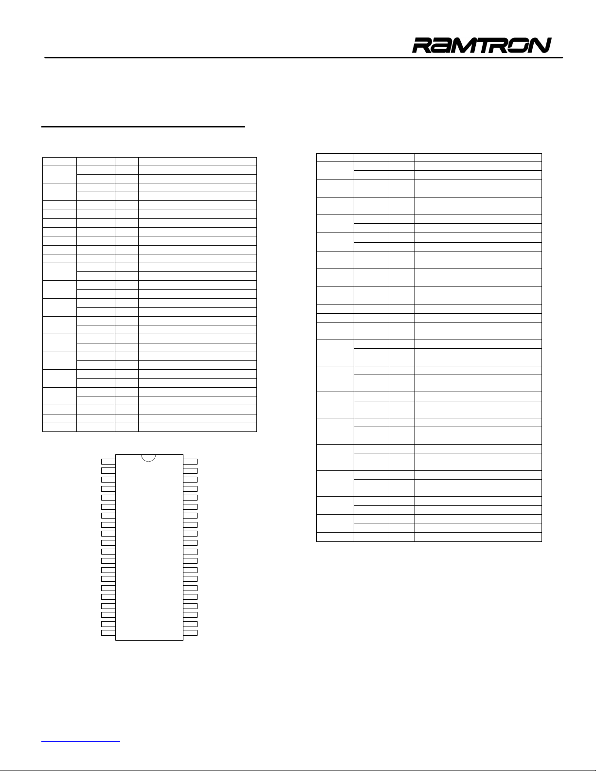
VRS51x540
VRS51x540 DIP-40 Pin Descriptions
TABLE 3: VRS51X540 IN DESCRIPTIONS FOR DIP-40 PACKAGE
DIP40 Name I/O Function
T2 I Timer 2 Clock Out
1
P1.0 I/O Bit 0 of Port 1
T2EX I Timer 2 Control
2
P1.1 I/O Bit 1 of Port 1
3 P1.2 I/O Bit 2 of Port 1
4 P1.3 I/O Bit 3 of Port 1
5 P1.4 I/O Bit 4 of Port 1
6 P1.5 I/O Bit 5 of Port 1
7 P1.6 I/O Bit 6 of Port 1
8 P1.7 I/O Bit 7 of Port 1
9 RESET I Reset
RXD I Receive Data
10
P3.0 I/O Bit 0 of Port 3
TXD O Transmit Data &
11
P3.1 I/O Bit 1 of Port 3
#INT0 I External Interrupt 0
12
P3.2 I/O Bit 2 of Port 3
#INT1 I External Interrupt 1
13
P3.3 I/O Bit 3 of Port 3
T0 I Timer 0
14
P3.4 I/O Bit 4 of Port 3
T1 I Timer 1 & 3
15
P3.5 I/O Bit 5 of Port
#WR O Ext. Memory Write
16
P3.6 I/O Bit 6 of Port 3
#RD O Ext. Memory Read
17
P3.7 I/O Bit 7 of Port 3
18 XTAL2 O Oscillator/Crystal Output
19 XTAL1 I Oscillator/Crystal In
20 VSS - Ground
T2 / P1.0
T2EX / P1.1
P1.2
P1.3
P1.4
P1.5
P1.6
P1.7
RESET
RXD / P3.0
TXD / P3.1
#INT0 / P3.2
#INT1 / P3.3
T0 / P3.4
T1 / P3.5
#WR / P3.6
#RD / P3.7
XTAL2
XTAL1
VSS
1
2
3
4
5
6
7
8
9
10
11
12
13
14
15
16
17
18
19
20
VRS51x540
DIP-40
40
VDD
39
P0.0 / AD0
38
P0.1 / AD1
37
P0.2 / AD2
36
P0.3 / AD3
35
P0.4 / AD4
34
P0.5 / AD5
33
P0.6 / AD6
32
P0.7 / AD7
31
#EA / VPP
30
ALE
29
PSEN
28
P2.7 / A15
27
P2.6 / A14
26
P2.5 / A13
25
P2.4 / A12
24
P2.3 / A11
23
P2.2 / A10
22
P2.1 / A9
21
P2.0 / A8
DIP40
21
22
23
24
25
26
27
28
29 #PSEN O Program Store Enable
30 ALE O Address Latch Enable
31
32
33
34
35
36
37
38
39
40 VDD - Supply input
Name I/O Function
P2.0 I/O Bit 0 of Port 2
A8 O Bit 8 of External Memory Address
P2.1 I/O Bit 1 of Port 2
A9 O Bit 9 of External Memory Address
P2.2 I/O Bit 2 of Port 2
A10 O Bit 10 of External Memory Address
P2.3 I/O Bit 3 of Port 2 &
A11 O Bit 11 of External Memory Address
P2.4 I/O Bit 4 of Port 2
A12 O Bit 12 of External Memory Address
P2.5 I/O Bit 5 of Port 2
A13 O Bit 13 of External Memory Address
P2.6 I/O Bit 6 of Port 2
A14 O Bit 14 of External Memory Address
P2.7 I/O Bit 7 of Port 2
A15 O Bit 15 of External Memory Address
#EA /
VPP
External Access
I
Flash programming voltage input
P0.7 I/O Bit 7 Of Port 0
AD7 I/O
Data/Address Bit 7 of External
Memory
P0.6 I/O Bit 6 of Port 0
AD6 I/O
Data/Address Bit 6 of External
Memory
P0.5 I/O Bit 5 of Port 0
AD5 I/O
Data/Address Bit 5 of External
Memory
P0.4 I/O Bit 4 of Port 0
AD4 I/O
Data/Address Bit 4 of External
Memory
P0.3 I/O Bit 3 Of Port 0
AD3 I/O
Data/Address Bit 3 of External
Memory
P0.2 I/O Bit 2 of Port 0
AD2 I/O
Data/Address Bit 2 of External
Memory
P0. 1 I/O Bit 1 of Port 0 & Data
AD1 I/O Address Bit 1 of External Memory
P0.0 I/O Bit 0 Of Port 0 & Data
AD0 I/O Address Bit 0 of External Memory
______________________________________________________________________________________________
www.ramtron.com page 4 of 40
VRS51x540
Instruction Set
The following tables describe the instruction set of the
VRS51x540. The instructions are functional and binary
code compatible with industry standard 8051s.
TABLE 4: LEGEND FOR INSTRUCTION SET TABLE
Symbol Function
A
Rn
Direct
@Ri
Rel
Bit
#data
#data 16
addr 16
addr 11
TABLE 5: VRS51X540 INSTRUCTION SET
Mnemonic Description
Arithmetic instructions
ADD A, Rn Add register to A
ADD A, direct Add direct byte to A
ADD A, @Ri Add data memory to A
ADD A, #data Add immediate to A
ADDC A, Rn Add register to A with carry
ADDC A, direct Add direct byte to A with carry
ADDC A, @Ri Add data memory to A with carry
ADDC A, #data Add immediate to A with carry
SUBB A, Rn Subtract register from A with borrow
SUBB A, direct Subtract direct byte from A with borrow
SUBB A, @Ri Subtract data mem from A with borrow
SUBB A, #data Subtract immediate from A with borrow
INC A Increment A
INC Rn Increment register
INC direct Increment direct byte
INC @Ri Increment data memory
DEC A Decrement A
DEC Rn Decrement register
DEC direct Decrement direct byte
DEC @Ri Decrement data memory
INC DPTR Increment data pointer
MUL AB Multiply A by B
DIV AB Divide A by B
DA A Decimal adjust A
Logical Instructions
ANL A, Rn AND register to A
ANL A, direct AND direct byte to A
ANL A, @Ri AND data memory to A
ANL A, #data AND immediate to A
ANL direct, A AND A to direct byte
ANL direct, #data AND immediate data to direct byte
ORL A, Rn OR register to A
ORL A, direct OR direct byte to A
ORL A, @Ri OR data memory to A
ORL A, #data OR immediate to A
ORL direct, A OR A to direct byte
ORL direct, #data OR immediate data to direct byte
XRL A, Rn Exclusive-OR register to A
XRL A, direct Exclusive-OR direct byte to A
XRL A, @Ri Exclusive-OR data memory to A
XRL A, #data Exclusive-OR immediate to A
XRL direct, A Exclusive-OR A to direct byte
XRL direct, #data Exclusive-OR immediate to direct byte
CLR A Clear A
CPL A Compliment A
SWAP A Swap nibbles of A
RL A Rotate A left
RLC A Rotate A left through carry
RR A Rotate A right
RRC A Rotate A right through carry
Accumulator
Register R0-R7
Internal register address
Internal register pointed to by R0 or R1 (except MOVX)
Two's complement offset byte
Direct bit address
8-bit constant
16-bit constant
16-bit destination address
11-bit destination address
Size
(bytes)
Instr. Cycles
1 1
2 1
1 1
2 1
1 1
2 1
1 1
2 1
1 1
2 1
1 1
2 1
1 1
1 1
2 1
1 1
1 1
1 1
2 1
1 1
1 2
1 4
1 4
1 1
1 1
2 1
1 1
2 1
2 1
3 2
1 1
2 1
1 1
2 1
2 1
3 2
1 1
2 1
1 1
2 1
2 1
3 2
1 1
1 1
1 1
1 1
1 1
1 1
1 1
Mnemonic Description
Boolean Instruction
CLR C Clear Carry bit
CLR bit Clear bit
SETB C Set Carry bit to 1
SETB bit Set bit to 1
CPL C Complement Carry bit
CPL bit Complement bit
ANL C,bit Logical AND between Carry and bit
ANL C,#bit Logical AND between Carry and not bit
ORL C,bit Logical ORL between Carry and bit
ORL C,#bit Logical ORL between Carry and not bit
MOV C,bit Copy bit value into Carry
MOV bit,C Copy Carry value into Bit
Data Transfer Instructions
MOV A, Rn Move register to A
MOV A, direct Move direct byte to A
MOV A, @Ri Move data memory to A
MOV A, #data Move immediate to A
MOV Rn, A Move A to register
MOV Rn, direct Move direct byte to register
MOV Rn, #data Move immediate to register
MOV direct, A Move A to direct byte
MOV direct, Rn Move register to direct byte
MOV direct, direct
MOV direct, @Ri Move data memory to direct byte
MOV direct, #data
MOV @Ri, A Move A to data memory
MOV @Ri, direct Move direct byte to data memory
MOV @Ri, #data Move immediate to data memory
MOV DPTR, #data
MOVC A, @A+DPTR
MOVC A, @A+PC Move code byte relative PC to A
MOVX A, @Ri Move external data (A8) to A
MOVX A, @DPTR Move external data (A16) to A
MOVX @Ri, A Move A to external data (A8)
MOVX @DPTR, A Move A to external data (A16)
PUSH direct Push direct byte onto stack
POP direct Pop direct byte from stack
XCH A, Rn Exchange A and register
XCH A, direct Exchange A and direct byte
XCH A, @Ri Exchange A and data memory
XCHD A, @Ri Exchange A and data memory nibble
Branching Instructions
ACALL addr 11 Absolute call to subroutine
LCALL addr 16 Long call to subroutine
RET Return from subroutine
RETI Return from interrupt
AJMP addr 11 Absolute jump unconditional
LJMP addr 16 Long jump unconditional
SJMP rel Short jump (relative address)
JC rel Jump on carry = 1
JNC rel Jump on carry = 0
JB bit, rel Jump on direct bit = 1
JNB bit, rel Jump on direct bit = 0
JBC bit, rel Jump on direct bit = 1 and clear
JMP @A+DPTR Jump indirect relative DPTR
JZ rel Jump on accumulator = 0
JNZ rel Jump on accumulator 1= 0
CJNE A, direct, rel Compare A, direct JNE relative
CJNE A, #d, rel Compare A, immediate JNE relative
CJNE Rn, #d, rel Compare reg, immediate JNE relative
CJNE @Ri, #d, rel
DJNZ Rn, rel Decrement register, JNZ relative
DJNZ direct, rel Decrement direct byte, JNZ relative
Miscellaneous Instruction
NOP No operation
Rn: Any of the register R0 to R7
@Ri: Indirect addressing using Register R0 or R1
#data: immediate Data provided with Instruction
#data16: Immediate data included with instruction
bit: address at the bit level
rel: relative address to Program counter from +127 to –128
Addr11: 11-bit address range
Addr16: 16-bit address range
#d: Immediate Data supplied with instruction
Move direct byte to direct byte
Move immediate to direct byte
Move immediate to data pointer
Move code byte relative DPTR to A
Compare ind, immediate JNE relative
Size
(bytes)
1 1
2 1
1 1
2 1
1 1
2 1
2 2
2 2
2 2
2 2
2 1
2 2
1 1
2 1
1 1
2 1
1 1
2 2
2 1
2 1
2 2
3 2
2 2
3 2
1 1
2 2
2 1
3 2
1 2
1 2
1 2
1 2
1 2
1 2
2 2
2 2
1 1
2 1
1 1
1 1
2 2
3 2
1 2
1 2
2 2
3 2
2 2
2 2
2 2
3 2
3 2
3 2
1 2
2 2
2 2
3 2
3 2
3 2
3 2
2 2
3 2
1 1
Instr. Cycles
______________________________________________________________________________________________
www.ramtron.com page 5 of 40
VRS51x540
Special Function Registers (SFR)
Addresses 80h to FFh of the SFR address space can be accessed in direct addressing mode only. The following table
lists the VRS51x540 Special Function Registers.
TABLE 6: SPECIAL FUNCTION REGISTERS (SFR)
SFR
Register
P0 80h - - - - - - - -
SP 81h - - - - - - - -
DPL 82h - - - - - - - -
DPH 83h - - - - - - - -
Reserved 84h - - - - - - - -
PCON 87h SMOD - - - GF1 GF0 PDOWN IDLE 00000000b
TCON 88h TF1 TR1 TF0 TR0 IE1 IT1 IE0 IT0 00000000b
TMOD 89h GATE1 C/T1 M1.1 M0.1 GATE0 C/T0 M1.0 M0.0 00000000b
TL0 8Ah - - - - - - - -
TL1 8Bh - - - - - - - -
TH0 8Ch - - - - - - - -
TH1 8Dh - - - - - - - -
P1 90h - - - - - - - -
SCON 98h SM0 SM1 SM2 REN TB8 RB8 TI RI 00000000b
SBUF 99h - - - - - - - -
WDTCON 9Fh WDTE - WDCLR - - WDPS2 WDPS1 WDPS0 0*0**000b
P2 A0h - - - - - - - -
IE A8h EA - ET2 ES ET1 EX1 ET0 EX0 00000000b
P3 B0h - - - - - - - -
IP B8h - - PT2 PS PT1 PX1 PT0 PX0 00000000b
SYSCON BFh WDRESET - - - - ALEI 0*****00b
T2CON C8h TF2 EXF2 RCLK TCLK EXEN2 TR2 C/T2 CP/RL2 00000000b
RCAP2L CAh - - - - - - - - 00000000b
RCAP2H CBh - - - - - - - - 00000000b
TL2 CCh - - - - - - - - 00000000b
TH2 CDh 00000000b
PSW D0h CY AC F0 RS1 RS0 OV - P 00000000b
ACC E0h - - - - - - - -
B F0h - - - - - - - -
SFR
Adrs
Bit 7 Bit 6 Bit 5 Bit 4 Bit 3 Bit 2 Bit 1 Bit 0 Reset Value
______________________________________________________________________________________________
www.ramtron.com page 6 of 40
VRS51x540
Program Memory Structure
Program Memory
The VRS51x540 includes 4k of on-chip Program Flash
memory.
FIGURE 3: VRS51X540 INTERNAL PROGRAM MEMORY
FFFh
VRS51x540
Flash Memory
(4K Bytes)
0000h
Program Status Word Register
The PSW register is a bit addressable register that
contains the status flags (CY, AC, OV, P), user flag
(F0) and register bank select bits (RS1, RS0) of the
8051 processor.
TABLE 7: PROGRAM STATUS WORD REGISTER (PSW) - SFR DOH
7 6 5 4 3 2 1 0
CY AC F0 RS1 RS0 OV - P
Bit Mnemonic Description
7 CY Carry Bit
6 AC Auxiliary Carry Bit from bit 3 to 4.
5 F0 User flag
4 RS1 R0-R7 Registers bank select bit 0
3 RS0 R0-R7 Registers bank select bit 1
2 OV Overflow flag
1 - 0 P Parity flag
RS1 RS0 Active Bank Address
0 0 0 00h-07h
0 1 1 08h-0Fh
1 0 2 10h-17h
1 1 3 18-1Fh
Data Pointer
The VRS51x540 has one 16-bit data pointer. The
DPTR is accessed through two SFR addresses: DPL
located at address 82h and DPH located at address
83h.
Data Memory
The VRS51x540 has a total of 128 Bytes of RAM
memory configured as the internal memory structure of
a standard 8051.
FIGURE 4: VRS51X540 DATA MEMORY
FFh
80h
7Fh
00h
128 bytes RAM
(indirect addressing only)
128 bytes RAM
(Can be accessed in indirect and
direct addressing mode)
(Direct addressing mode only)
Lower 128 bytes (00h to 7Fh, Bank 0 & Bank 1)
The lower 128 bytes of data memory (from 00h to 7Fh)
is summarized as follows:
• Address range 00h to 7Fh can be accessed in
direct and indirect addressing modes.
• Address range 00h to 1Fh includes R0-R7
registers area.
• Address range 20h to 2Fh is bit addressable.
• Address range 30h to 7Fh is not bit addressable
and can be used as general-purpose storage.
.
FIGURE 5: VRS51X540 INTERNAL RAM STRUCTURE
SFR Area
Direct or Bit Access Only
DPH
DPL
SP
P0
7Fh
30h
2Fh
20h
18h
10h
08h
00h
80 Bytes of
General Purpose RAM
7F 7E 7D 7C 7B 7A 79 78
77 76 75 74 73 72 71 70
0F 0E 0D 0C 0B 0A 09 08
07 06 05 04 03 02 01 00
R7
-
Registers Bank 3
R0
R7
-
Registers Bank 2
R0
R7
Registers Bank 1
-
R0
R7
Registers Bank 0
-
R0
85 84 83 82 81 80
87 86
SFR
FFh
80h
______________________________________________________________________________________________
www.ramtron.com page 7 of 40
VRS51x540
Description of Peripherals
System Control Register
The SYSCON Register is used for system control and
is described in the following table. The WDRESET bit
(7) indicates whether the system has been reset due to
the overflow of the Watchdog Timer.
Bit 0 of the SYSCON register is the ALE output inhibit
bit. Setting this bit to a 1 will inhibit the Fosc/6 clock
signal output to the ALE pin.
TABLE 8: SYSTEM CONTROL REGISTER (SYSCON) – SFR BFH
7 6 5 4 3 2 1 0
WDRESET
Unused
Bit Mnemonic Description
7
6 Unused 5 Unused 4 Unused 3 Unused 2 Unused 1 Unused 0 ALEI ALE output inhibit bit, which is used to
WDRESET
This is the Watchdog Timer reset bit. It
will be set to 1 when the reset signal
generated by WDT overflows.
reduce EMI.
XRAME
ALEI
These power saving modes are controlled by the
PDOWN and IDLE bits of the PCON register at
address 87h.
TABLE 9: POWER CONTROL REGISTER (PCON) - SFR 87H
7 6 5 4 3 2 1 0
Unused RAM1 RAM0
Bit Mnemonic Description
7 SMOD 1: Double the baud rate of the serial port
frequency that was generated by Timer 1.
0: Normal serial port baud rate generated by
Timer 1.
6
5
4
3 GF1 General Purpose Flag
2 GF0 General Purpose Flag
1 PDOWN Power down mode control bit
0 IDLE Idle mode control bit
Power Control Register
The VRS51x540 provides two power saving modes:
Idle and Power Down. These two modes serve to
reduce the power consumption of the device.
In Idle mode, the processor is stopped but the oscillator
continues to run. The content of the RAM, I/O state
and SFR registers are maintained and the Timer and
external interrupts are left operational. The processor
will be woken up when an external event, triggering an
interrupt, occurs.
In Power Down mode, the oscillator and peripherals of
the VRS51x540 are disabled. The contents of the
RAM and the SFR registers, however, are maintained.
The minimum VCC in Power Down mode is 2V.
______________________________________________________________________________________________
www.ramtron.com page 8 of 40
VRS51x540
Input/Output Ports
The VRS51x540 has a total of 32 bi-directional I/O
lines grouped into four 8-bit I/O ports. These I/Os can
be individually configured as inputs or outputs.
With the exception of the P0 I/Os, which are of the
open drain type, each I/O is made of a transistor
connected to ground and a weak pull-up resistor.
Writing a 0 in a given I/O port bit register will activate
the transistor connected to Vss, this will bring the I/O to
a LOW level.
Writing a 1 into a given I/O port bit register de-activates
the transistor between the pin and ground. In this case
the pull-up resistor will bring the corresponding pin to a
HIGH level.
To use a given I/O as an input, a 1 must be written into
its associated port register bit. By default, upon reset
all I/Os are configured as inputs.
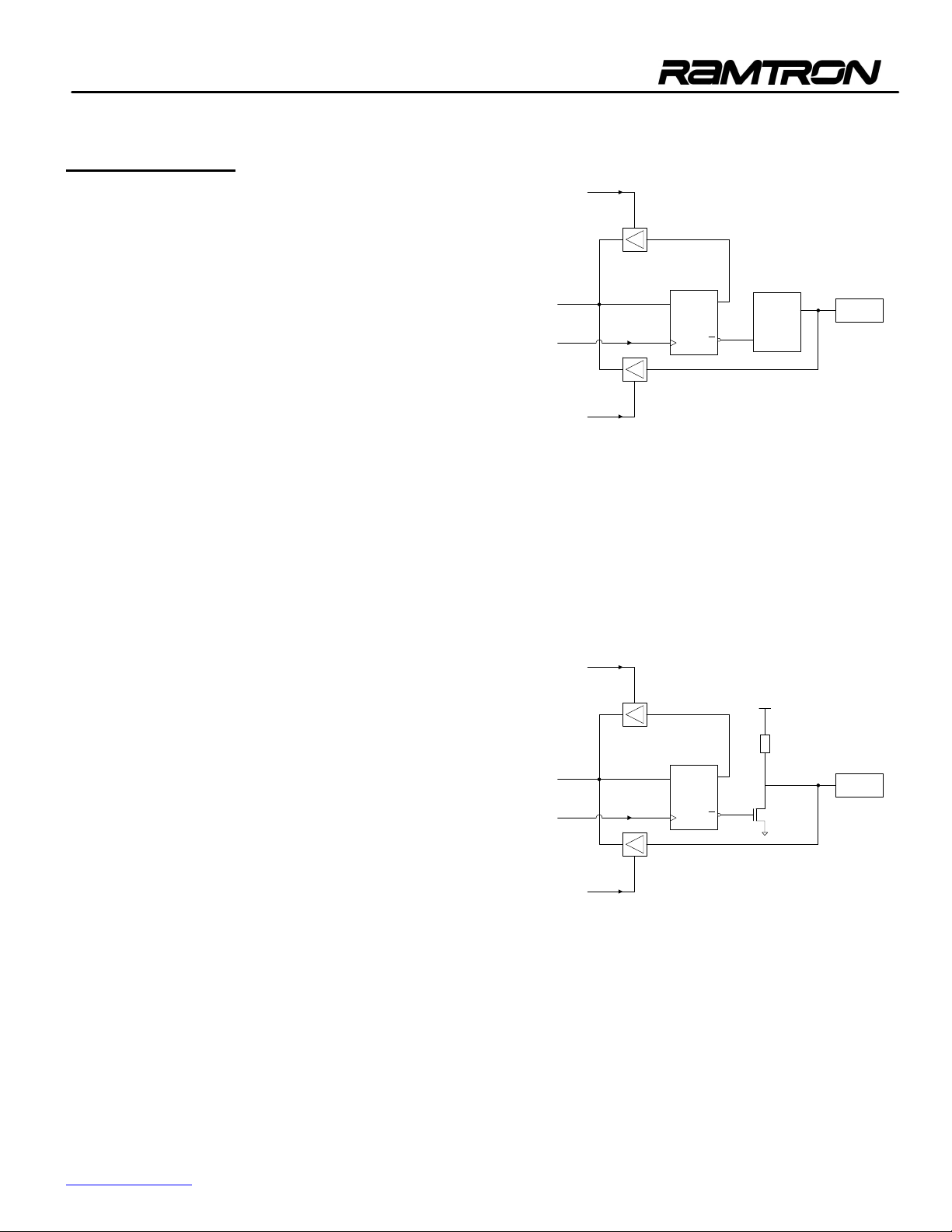
General Structure of an I/O Port
The following elements establish the link between the
core unit and the pins of the microcontroller:
• Special Function Register (same name as port)
• Output Stage Amplifier (the structure of this
element varies with its auxiliary function)
From the next figure, one can see that the D flip-flop
stores the value received from the internal bus after
receiving a write signal from the core. Also, note that
the Q output of the flip-flop can be linked to the internal
bus by executing a read instruction.
This is how one would read the content of the register.
It is also possible to link the value of the pin to the
internal bus. This is done by the “read pin” instruction.
In short, the user may read the value of the register or
the pin.
FIGURE 6: INTERNAL STRUCTURE OF ONE OF THE FOUR I/O PORT LINES
Read Register
D Flip-Flop
Q
Output
Q
Stage
IC Pin
Internal Bus
Write to
Register
Read Pin
Structure of the P1, P2, P3
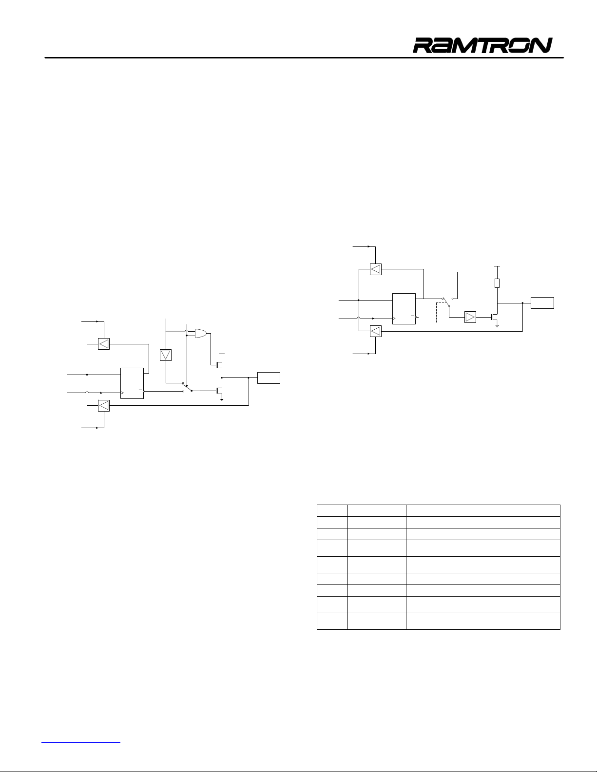
The following figure gives a general idea of the
structure P1, P2 and P3 ports. Note that the figure
below does not show the intermediary logic that
connects the output of the register and the output stage
together because this logic varies with the auxiliary
function of each port.
FIGURE 7: GENERAL STRUCTURE OF THE OUTPUT STAGE OF P1, P2 AND P3
Read Register
Vcc
Pull-up
Network
D Flip-Flop
Q
Q
X1
IC Pin
Internal Bus
Write to
Register
Read Pin
Each line may be used independently as a logical
input or output. When used as an input, as mentioned
earlier, the corresponding port register bit must be
high.
______________________________________________________________________________________________
www.ramtron.com page 9 of 40
VRS51x540
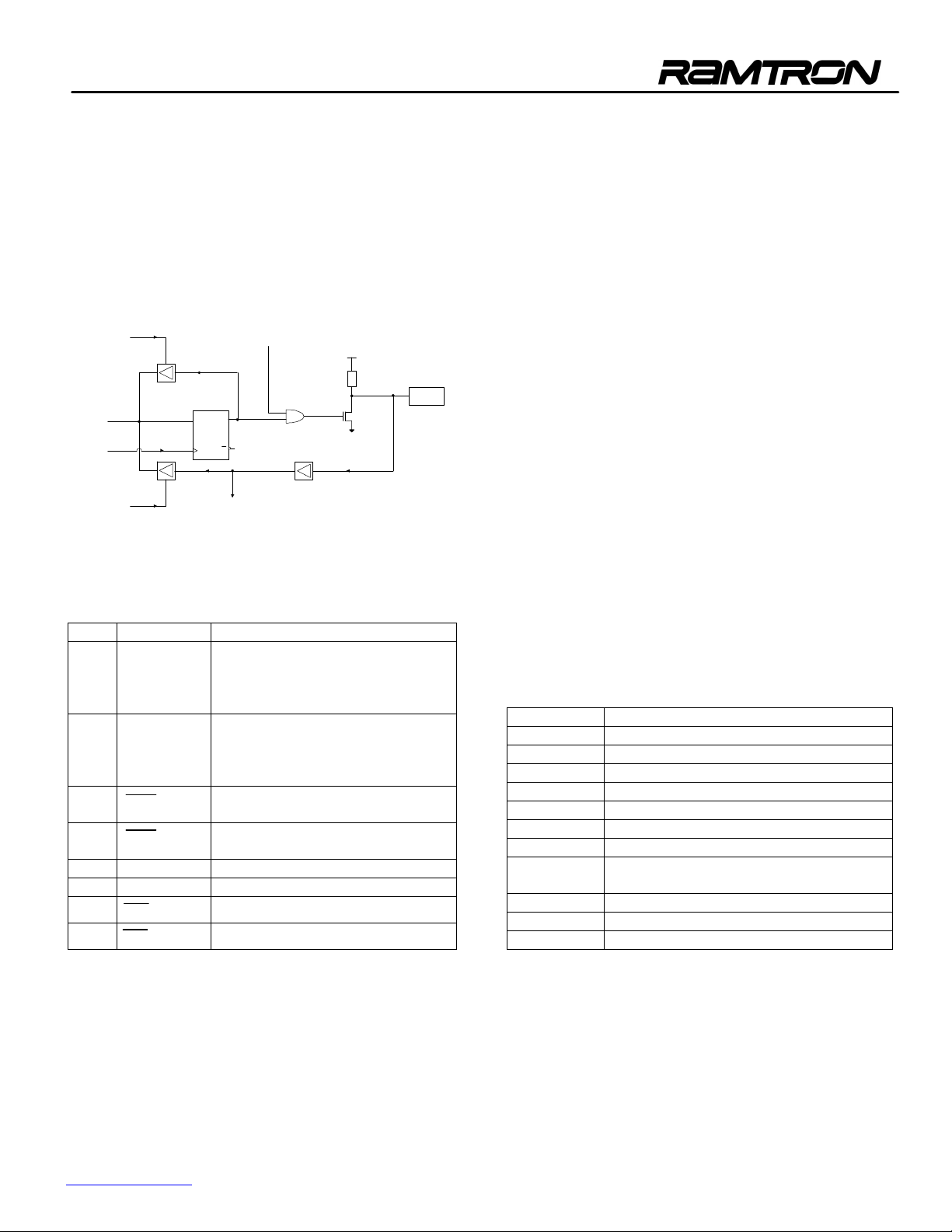
Structure of Port 0
The internal structure of P0 is shown below. The
auxiliary function of this port requires a particular logic.
As opposed to the other ports, P0 is truly bi-directional.
In other words, when used as an input, it is considered
to be in a floating logical state (high impedance state).
This arises from the absence of the internal pull-up
resistance. The pull-up resistance is actually replaced
by a transistor that is only used when the port is
configured to access the external memory/data bus
(EA=0).
When used as an I/O port, P0 acts as an open drain
port and the use of an external pull-up resistor is likely
to be required for most applications.
FIGURE 8: PORT P0’S PARTICULAR STRUCTURE
Internal Bus
Write to
Register
Read Register
D Flip-Flop
Read Pin
Q
Q
Address A0/A7
Control
Vcc
IC Pin
X1
When P0 is used as an external memory bus input (for
a MOVX instruction, for example), the outputs of the
register are automatically forced to 1.
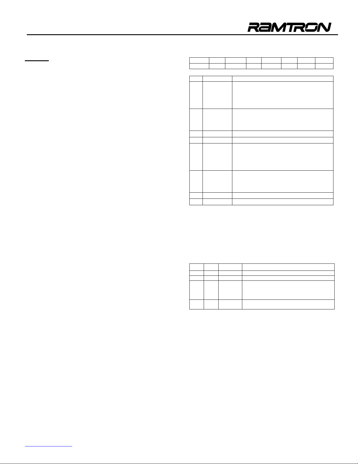
Port P0 and P2 as Address and Data Bus
The output stage may receive data from two sources
• The outputs of register P0 or the bus address
itself, multiplexed with the data bus for P0.
• The outputs of the P2 register or the high byte
(A8 through A15) of the bus address for the P2
port.
FIGURE 9: P2 PORT STRUCTURE
Read Register
Vcc
Pull-up
Network
IC Pin
X1
Internal Bus
Write to
Register
Read Pin
D Flip-Flop
Address
Q
Q
Control
When the ports are used as an address or data bus,
the special function registers P0 and P2 are
disconnected from the output stage. The 8-bits of the
P0 register are forced to 1 and the content of the P2
register remains constant.
Auxiliary Port 1 Functions
The port 1 I/O pins are shared with the Timer 2 EX and
T2 inputs as shown below:
Pin Mnemonic Function
P1.0 T2 Timer 2 counter input
P1.1 T2EX Timer2 Auxiliary input
P1.2
P1.3
P1.4
P1.5
P1.6
P1.7
______________________________________________________________________________________________
www.ramtron.com page 10 of 40
VRS51x540
Auxiliary P3 Port Functions
The Port 3 I/O pins are shared with the UART
interface, INT0 and INT1 interrupts, Timer 0 and Timer
1 inputs and finally the #WR and #RD lines when
external memory access is performed.
FIGURE 10: P3 PORT STRUCTURE
Read Register
Internal Bus
Write to
Register
Read Pin
D Flip-Flop
The following table describes the auxiliary function of
the port 3 I/O pins.
TABLE 10: P3 AUXILIARY FUNCTION TABLE
Pin Mnemonic Function
P3.0 RXD Serial Port:
P3.1 TXD Serial Port:
P3.2
P3.3
INT0
INT1
P3.4 T0 Timer 0 Counter Input
P3.5 T1 Timer 1 Counter Input
P3.6
P3.7
WR
RD
Auxiliary
Function: Output
Vcc
IC Pin
Q
Q
Auxiliary
Function: Input
X1
Receive data in asynchronous
mode. Input and output data in
synchronous mode.
Transmit data in asynchronous
mode. Output clock value in
synchronous mode.
External Interrupt 0
Timer 0 Control Input
External Interrupt 1
Timer 1 Control Input
Write signal for external memory
Read signal for external memory
Software Particularities Concerning the Ports
Some instructions allow the user to read the logic state
of the output pin, while others allow the user to read
the content of the associated port register. These
instructions are called read-modify-write instructions. A
list of these instructions may be found in the table
below.
Upon execution of these instructions, the content of the
port register (at least 1-bit) is modified. The other read
instructions take the present state of the input into
account. For example, the instruction ANL P3, #01h
obtains the value in the P3 register; performs the
desired logic operation with the constant 01h; and recopies the result into the P3 register. When users want
to take the present state of the inputs into account,
they must first read these states and perform an AND
operation between the reading and the constant.
MOV A, P3; State of the inputs in the accumulator
ANL A, #01; AND operation between P3 and 01h
When the port is used as an output, the register
contains information on the state of the output pins.
Measuring the state of an output directly on the pin is
inaccurate because the electrical level depends mostly
on the type of charge that is applied to it. The functions
shown below take the value of the register rather than
that of the pin.
TABLE 11: LIST OF INSTRUCTIONS THAT READ AND MODIFY THE PORT USING REGISTER
VALUES
Instruction Function
ANL Logical AND ex: ANL P0, A
ORL Logical OR ex: ORL P2, #01110000B
XRL Exclusive OR ex: XRL P1, A
JBC Jump if the bit of the port is set to 0
CPL Complement one bit of the port
INC Increment the port register by 1
DEC Decrement the port register by 1
DJNZ Decrement by 1 and jump if the result
is not equal to 0
MOV P., C Copy the held bit C to the port
CLR P.x Set the port bit to 0
SETB P.x Set the port bit to 1
______________________________________________________________________________________________
www.ramtron.com page 11 of 40

VRS51x540
Port Operation Timing
Writing to a Port (Output)
When an operation results in a modification of the
content in a port register, the new value is placed at the
output of the D flip-flop during the T12 period of the last
machine cycle that the instruction needed to execute.
It is important to note, however, that the output stage
only samples the output of the registers on the P1
phase of each period. It follows the new value
appearing at the output after the T12 period of the
following machine cycle.
Reading a Port (Input)
The reading of an I/O pin takes place:
• During T9 cycle for P0, P1
• During T10 cycle for P2, P3
• When the ports are configured as I/Os
•
In order to be sampled, the signal duration present on
the I/O inputs must be longer than Fosc/12.
I/O Ports Driving Capability
The maximum allowable continuous current that the
device can sink on an I/O port is defined by the
following:
Maximum sink current on one given I/O 10mA
Maximum total sink current for P0 26mA
Maximum total sink current for P1, 2, 3 15mA
Maximum total sink current on all I/O 71mA
It is not recommended to exceed the sink current
outlined in the above table. Doing so is likely to make
the low-level output voltage exceed the device’s
specification and it is likely to affect device reliability.
The VRS51x540 I/O ports are not designed to source
current.
______________________________________________________________________________________________
www.ramtron.com page 12 of 40
VRS51x540
Timers
The VRS51x540 includes three 16-bit timers: T0, T1
and T2.
The timers can operate in two specific modes:
• Event counting mode
• Timer mode
When operating in counting mode, the counter is
incremented each time an external event, such as a
transition in the logical state of the timer input (T0, T1,
T2 input), is detected. When operating in timer mode,
the counter is incremented by the microcontroller’s
direct clock pulse or by a divided version of this pulse.
Timer 0 and Timer 1
Timers 0 and 1 have four modes of operation. These
modes allow the user to change the size of the
counting register or to authorize an automatic reload
when provided with a specific value. Timer 1 can also
be used as a baud rate generator to generate
communication frequencies for the serial interface.
Timer 1 and Timer 0 are configured by the TMOD and
TCON registers.
TABLE 12: TIMER MODE CONTROL REGISTER (TMOD) – SFR 89H
7 6 5 4 3 2 1 0
GATE C/T M1 M0 GATE C/T M1.0 M0.0
Bit Mnemonic Description
7 GATE1 1: Enables external gate control (pin INT1 for
6 C/T1 Selects timer or counter operation (Timer 1).
5 M1.1
4 M0.1
3 GATE0
2 C/T0
1 M1.0
0 M0.0
Counter 1). When INT1 is high, and TRx bit is
set (see TCON register), a counter is
incremented every falling edge on the T1IN
input pin.
1 = A counter operation is performed
0 = The corresponding register will function
as a timer.
Selects mode for Timer/Counter 1
Selects mode for Timer/Counter 1
If set, enables external gate control (pin INT0
for Counter 0). When INT0 is high, and TRx
bit is set (see TCON register), a counter is
incremented every falling edge on the T0IN
input pin.
Selects timer or counter operation (Timer 0).
1 = A counter operation is performed
0 = The corresponding register will function
as a timer.
Selects mode for Timer/Counter 0.
Selects mode for Timer/Counter 0.
The table below summarizes the four modes of
operation of timers 0 and 1. The timer-operating mode
is selected by the bits M1 and M0 of the TMOD
register.
TABLE 13: TIMER/COUNTER MODE DESCRIPTION SUMMARY
M1 M0 Mode Function
0 0 Mode 0 13-bit Counter
0 1 Mode 1 16-bit Counter
1 0 Mode 2 8-bit auto-reload Counter/Timer. The reload
1 1 Mode 3 If Timer 1 M1 and M0 bits are set to 1, Timer 1
value is kept in TH0 or TH1, while TL0 or TL1
is incremented every machine cycle. When TLx
overflows, the value of THx is copied to TLx.
stops.
______________________________________________________________________________________________
www.ramtron.com page 13 of 40

VRS51x540
Timer 0/ Timer 1 Counter / Timer Functions
Timing Function
When operating as a timer, the counter is automatically
incremented at every system cycle (Fosc/12). A flag is
raised in the event that an overflow occurs and the
counter acquires a value of zero. These flags (TF0 and
TF1) are located in the TCON register.
TABLE 14: TIMER 0 AND 1 CONTROL REGISTER (TCON) –SFR 88H
7 6 5 4 3 2 1 0
TF1 TR1 TF0 TR0 IE1 IT1 IE0 IT0
Bit Mnemonic Description
7 TF1 Timer 1 Overflow Flag. Set by hardware on
6 TR1 Timer 1 Run Control Bit. Set/cleared by
5 TF0
4 TR0
3 IE1
2 IT1
1 IE0
0 IT0
Counting Function
When operating as a counter, the timer’s register is
incremented at every falling edge of the T0, T1 and T2
signals located at the input of the timer. In this case,
the signal is sampled at the T10 phase of each
machine cycle for Timer 0, Timer 1 and T9 for Timer 2.
When the sampler sees a high immediately followed by
a low in the next machine cycle, the counter is
incremented. Two system cycles are required to detect
and record an event. This reduces the counting
frequency by a factor of 24 (24 times less than the
oscillator’s frequency).
Timer/Counter overflow. Cleared by
hardware on Timer/Counter overflow.
Cleared by hardware when processor
vectors to interrupt routine.
software to turn Timer/Counter on or off.
Timer 0 Overflow Flag. Set by hardware on
Timer/Counter overflow. Cleared by
hardware when processor vectors to
interrupt routine.
Timer 0 Run Control Bit. Set/cleared by
software to turn Timer/Counter on or off.
Interrupt Edge Flag. Set by hardware when
external interrupt edge is detected. Cleared
when interrupt processed.
Interrupt 1 Type Control Bit. Set/cleared by
software to specify falling edge/low level
triggered external interrupts.
Interrupt 0 Edge Flag. Set by hardware
when external interrupt edge is detected.
Cleared when interrupt processed.
Interrupt 0 Type control bit. Set/cleared by
software to specify falling edge/low level
triggered external interrupts.
Operating Modes
The user may change the operating mode by varying
the M1 and M0 bits of the TMOD SFR.
Mode 0
A schematic representation of this mode of operation
can be found in Figure 11. From the figure, we notice
that the timer operates as an 8-bit counter preceded by
a divide-by-32 prescaler composed of the 5 LSBs of
TL1. The register of the counter is configured to be 13
bits long. When an overflow causes the value of the
register to roll over to 0, the TFx interrupt signal goes
to 1. The count value is validated as soon as TRx goes
to 1 and the GATE bit is 0, or when INTx is 1.
FIGURE 11: TIMER/COUNTER 1 MODE 0: 13-BIT COUNTER
CLK ÷12
TL1
0 74
Mode 0
Mode 1
TH1
0 7
TF1
INT
T1PIN
TR1
GATE
INT1 PIN
C/T =0
0
1
C/T =1
Control
CLK
Mode 1
Mode 1 is almost identical to Mode 0. They differ in that
in Mode 1, the counter uses the full 16-bits and has no
prescaler.
Mode 2
In this mode, the register of the timer is configured as
an 8-bit automatically re-loadable counter. In Mode 2, it
is the lower byte TLx that is used as the counter. In the
event of a counter overflow, the TFx flag is set to 1 and
the value contained in THx, which is preset by
software, is reloaded into the TLx counter. The value of
THx remains unchanged.
______________________________________________________________________________________________
www.ramtron.com page 14 of 40

VRS51x540
FIGURE 12: TIMER/COUNTER 1 MODE 2: 8-BIT AUTOMATIC RELOAD
CLK
T1 Pin
TR1
GATE
INT0 PIN
Mode 3
In Mode 3, Timer 1 is blocked as if its control bit, TR1,
was set to 0. In this mode, Timer 0’s registers TL0 and
TH0 are configured as two separate 8-bit counters.
Also, the TL0 counter uses Timer 0’s control bits C/T,
GATE, TR0, INT0, TF0 and the TH0 counter is held in
Timer Mode (counting machine cycles) and gains
control over TR1 and TF1 from Timer 1. At this point,
TH0 controls the Timer 1 interrupt.
÷12
C/T =0
0
C/T=1
1
Control
TL1
0 7
0 7
TH1
TF1
Reload
INT
FIGURE 13: TIMER/COUNTER 0 MODE 3
CLK ÷12
0
1
T0PIN
TR0
GATE
INT0 PIN
C/T =0
C/T =1
Control
Control
TH0
0 7
CLK
0 7
CLK
TF1
TF0
TR1
INTERRUPT
TL0
INTERRUPT
______________________________________________________________________________________________
www.ramtron.com page 15 of 40

VRS51x540
Timer 2
Timer 2 of the VRS51x540 is a 16-bit Timer/Counter.
Similar to timers 0 and 1, Timer 2 can operate either as
an event counter or as a timer. The user may switch
functions by writing to the C/T2 bit located in the
T2CON special function register. Timer 2 has three
operating modes: “Auto-Load” “Capture”, and “Baud
Rate Generator”. The T2CON SFR configures the
modes of operation of Timer 2. The following table
describes each bit in the T2CON special function
register.
TABLE 15: TIMER 2 CONTROL REGISTER (T2CON) –SFR C8H
7 6 5 4 3 2 1 0
TF2 EXF2 RCLK TCLK EXEN2 TR2 C/T2 CP/RL2
Bit Mnemonic Description
7 TF2
6 EXF2
5 RCLK
4 TCLK
3 EXEN2
2 TR2
1
C/T2
Timer 2 Overflow Flag: Set by an overflow
of Timer 2 and must be cleared by
software. TF2 will not be set when either
RCLK =1 or TCLK =1.
Timer 2 external flag change in state occurs
when either a capture or reload is caused
by a negative transition on T2EX and
EXEN2=1. When Timer 2 is enabled,
EXF=1 will cause the CPU to Vector to the
Timer 2 interrupt routine. Note that EXF2
must be cleared by software.
Serial Port Receive Clock Source.
1: Causes Serial Port to use Timer 2
overflow pulses for its receive clock in
modes 1 and 3.
0: Causes Timer 1 overflow to be used for
the Serial Port receive clock.
Serial Port Transmit Clock.
1: Causes Serial Port to use Timer 2
overflow pulses for its transmit clock in
modes 1 and 3.
0: Causes Timer 1 overflow to be used for
the Serial Port transmit clock.
Timer 2 External Mode Enable.
1: Allows a capture or reload to occur as a
result of a negative transition on T2EX if
Timer 2 is not being used to clock the Serial
Port.
0: Causes Timer 2 to ignore events at
T2EX.
Start/Stop Control for Timer 2.
1: Start Timer 2
0: Stop Timer 2
Timer or Counter Select (Timer 2)
1: External event counter falling edge
triggered.
0: Internal Timer (OSC/12)
0
CP/RL2
Capture/Reload Select.
1: Capture of Timer 2 value into RCAP2H,
RCAP2L is performed if EXEN2=1 and a
negative transitions occurs on the T2EX
pin. The capture mode requires RCLK and
TCLK to be 0.
0: Auto-reload reloads will occur either with
Timer 2 overflows or negative transitions at
T2EX when EXEN2=1. When either RCK
=1 or TCLK =1, this bit is ignored and the
timer is forced to auto-reload on Timer 2
overflow.
As shown below, there are different possible
combinations of control bits that may be used for the
mode selection of Timer 2.
TABLE 16: TIMER 2 MODE SELECTION BITS
RCLK + TCLK
0 0 1
0 1 1
1 X 1
CP/RL2
TR2 MODE
16-bit AutoReload Mode
16-bit Capture
Mode
Baud Rate
Generator Mode
X X 0 Off
The details of each mode are described as follows.
Capture Mode
In Capture Mode the EXEN2 bit value defines if the
external transition on the T2EX pin will be able to
trigger the capture of the timer value.
When EXEN2 = 0, Timer 2 acts as a 16-bit timer or
counter, which, upon overflowing, will set bit TF2
(Timer 2 overflow bit). This overflow can be used to
generate an interrupt.
FIGURE 14: TIMER 2 IN CAPTURE MODE
F
T2 Pin
T2 EX Pin
OSC
÷12
EXEN2
C/T2
0
1
TIMER
COUNTER
TR2
TL2
0 7
0 7
RCAP2L RCAP2H
TH2
0 7
0 7
EXF2
TF2
Timer 2
Interrupt
______________________________________________________________________________________________
www.ramtron.com page 16 of 40

VRS51x540
When EXEN2 = 1, the above still applies. Additionally,
it is possible to allow a 1 to 0 transition at the T2EX
input to cause the current value stored in the Timer 2
registers (TL2 and TH2) to be captured by the RCAP2L
and RCAP2H registers. Furthermore, the transition at
T2EX causes bit EXF2 in T2CON to be set, and EXF2,
like TF2, can generate an interrupt. Note that both
EXF2 and TF2 share the same interrupt vector.
Auto-Reload Mode
In this mode, there are also two options. The user may
choose either option by writing to bit EXEN2 in T2CON.
If EXEN2 = 0, when Timer 2 rolls over, it not only sets
TF2, but also causes the Timer 2 registers to be
reloaded with the 16-bit value in the RCAP2L and
RCAP2H registers previously initialised. In this mode,
Timer 2 can be used as a baud rate generator source
for the serial port.
If EXEN2=1, then Timer 2 still performs the above
operation, but a 1 to 0 transition at the external T2EX
input will also trigger an anticipated reload of the Timer
2 with the value stored in RCAP2L, RCAP2H and set
EXF2.
F
T2 Pin
T2 EX Pin
÷2
OSC
TIMER
EXEN2
C/T2
0
COUNTER
1
TR2
Timer 1 Overflow
TL2
0 7
0 7
RCAP2L RCAP2H
1
0
TCLK
0
1
÷2
SMOD
TH2
0 7
0 7
1
0
RCLK
EXF2
TX Clock
÷16
RX Clock
÷16
Timer 2
Interrupt
Request
FIGURE 15: TIMER 2 IN AUTO-RELOAD MODE
F
T2 Pin
T2 EX Pin
÷12
OSC
TIMER
EXEN2
C/T2
0
COUNTER
1
TR2
TL2
0 7
0 7
RCAP2L RCAP2H
TH2
0 7
0 7
EXF2
Timer 2
Interrupt
TF2
Baud Rate Generator Mode
The baud rate generator mode is activated when RCLK
is set to 1 and/or TCLK is set to 1. This mode will be
described in the serial port section.
FIGURE 16: TIMER 2 IN AUTOMATIC BAUD GENERATOR MODE
______________________________________________________________________________________________
www.ramtron.com page 17 of 40

VRS51x540
Serial Port
The serial port included in the VRS51x540 can operate
in full duplex; in other words, it can transmit and
receive data simultaneously. This occurs at the same
speed if one timer is assigned as the clock source for
both transmission and reception, and at different
speeds if transmission and reception are each
controlled by their own timer.
The serial port receive is buffered, which means that it
can begin reception of a byte even if the one previously
received byte has not been retrieved from the receive
register by the processor. However, if the first byte still
has not been read by the time reception of the second
byte is complete, the byte present in the receive buffer
will be lost.
The SBUF register provides access to the transmit and
receive registers of the serial port. Reading from the
SBUF register will access the receive register, while a
write to the SBUF loads the transmit register.
Serial Port Control Register
The SCON (serial port control) register contains control
and status information, and includes the 9th data bit for
transmit/receive (TB8/RB8 if required), mode selection
bits and serial port interrupt bits (TI and RI).
TABLE 17: SERIAL PORT CONTROL REGISTER (SCON) – SFR 98H
7 6 5 4 3 2 1 0
SM0 SM1 SM2 REN TB8 RB8 TI RI
Bit Mnemonic Description
7 SM0 Bit to select mode of operation (see table
6 SM1 Bit to select mode of operation (see table
5 SM2
4 REN
3 TB8
below)
below)
Multiprocessor communication is possible
in modes 2 and 3.
In modes 2 or 3 if SM2 is set to 1, RI will
not be activated if the received 9th data bit
(RB8) is 0.
In Mode 1, if SM2 = 1 then RI will not be
activated if a valid stop bit was not
received.
Serial Reception Enable Bit
This bit must be set by software and
cleared by software.
1: Serial reception enabled
0: Serial reception disabled
9th data bit transmitted in modes 2 and 3
This bit must be set by software and
cleared by software.
2 RB8
1 TI
0 RI
9th data bit received in modes 2 and 3.
In Mode 1, if SM2 = 0, RB8 is the stop bit
that was received.
In Mode 0, this bit is not used.
This bit must be cleared by software.
Transmission Interrupt flag.
Automatically set to 1 when:
• The 8th bit has been sent in Mode 0.
• Automatically set to 1 when the stop bit
has been sent in the other modes.
This bit must be cleared by software.
Reception Interrupt flag
Automatically set to 1 when:
• The 8th bit has been received in Mode 0.
• Automatically set to 1 when the stop bit
has been sent in the other modes (see
SM2 exception).
This bit must be cleared by software.
TABLE 18: SERIAL PORT MODES OF OPERATION
SM0 SM1 Mode Description Baud Rate
0 0 0 Shift Register F
osc
/12
0 1 1 8-bit UART Variable
1 0 2 9-bit UART F
osc
F
osc
/64 or
/32
1 1 3 9-bit UART Variable
Modes of Operation
The VRS51x540 serial port can operate in four different
modes. In all four modes, a transmission is initiated by
an instruction that uses the SBUF SFR as a destination
register. In Mode 0, reception is initiated by setting RI
to 0 and REN to 1. An incoming start bit initiates
reception in the other modes provided that REN is set
to 1. The following paragraphs describe the four
modes.
______________________________________________________________________________________________
www.ramtron.com page 18 of 40

VRS51x540
Mode 0
In this mode, the serial data exits and enters through
the RXD pin. TXD is used to output the shift clock. The
signal is composed of 8 data bits starting with the LSB.
The baud rate in this mode is 1/12 the oscillator
frequency.
Q
ZERO DETECTOR
RX Control Unit
1 1 1 1 1 1 1 0
Internal Bus
SBUF
TX Control Unit
TI
RI
Shift Register
SBUF
Internal Bus
Shift
Receive
Shift
Send
Serial Port
Interrupt
Shift
Clock
RXD P3.0
READ SBUF
RXD P3.0
TXD P3.1
Fosc/12
RI
REN
1
RXD P3.0
Input Function
S
D
CLK
Start
TX Clock
RX Clock
Start Shift
Write to
SBUF
FIGURE 17: SERIAL PORT MODE 0 BLOCK DIAGRAM
Transmission in Mode 0
Any instruction that uses SBUF as a destination
register may initiate a transmission. The “write to
SBUF” signal also loads a 1 into the 9th position of the
transmit shift register and tells the TX control block to
begin a transmission. The internal timing is such that
one full machine cycle will elapse between a write to
SBUF instruction and the activation of SEND.
The SEND signal enables the output of the shift
register to the alternate output function line of P3.0 and
enables SHIFT CLOCK to the alternate output function
line of P3.1. SHIFT CLOCK is high during T11, T12
and T1, T2 and T3, T4 of every machine cycle and low
during T5, T6, T7, T8, T9 and T10. At T12 of every
machine cycle in which SEND is active and the
contents of the transmit shift register are shifted to the
right by one position.
Zeros come in from the left as data bits shift out to the
right. The TX control block sends its final shift and deactivates SEND while setting T1 after one condition is
fulfilled: When the MSB of the data byte is at the output
position of the shift register; the 1 that was initially
loaded into the 9th position is just to the left of the MSB;
and all positions to the left of that contain zeros. Once
these conditions are met, the de-activation of SEND
and the setting of T1 occur at T1 of the 10th machine
cycle after the “write to SBUF” pulse.
Reception in Mode 0
When REN and R1 are set to 1 and 0 respectively,
reception is initiated. The bits 11111110 are written to
the receive shift register at T12 of the next machine
cycle by the RX control unit. In the following phase, the
RX control unit will activate RECEIVE.
SHIFT CLOCK to the alternate output function line of
P3.1 is enabled by RECEIVE. At every machine cycle,
SHIFT CLOCK makes transitions at T5 and T11. The
contents of the receive shift register are shifted one
position to the left at T12 of every machine in which
RECEIVE is active. The value that comes in from the
right is the value that was sampled at the P3.0 pin at
T10 of the same machine cycle.
1’s are shifted out to the left as data bits are shifted in
from the right. The RX control block is flagged to do
one last shift and load SBUF when the 0 that was
initially loaded into the rightmost position arrives at the
leftmost position in the shift register.
______________________________________________________________________________________________
www.ramtron.com page 19 of 40

VRS51x540
Mode 1
For an operation in Mode 1, 10 bits are transmitted
through TXD or received through RXD. The
transactions are composed of: a Start bit (Low), 8 data
bits (LSB first) and one Stop bit (high). The reception is
completed once the Stop bit sets the RB8 flag in the
SCON register. Either Timer 1 or Timer 2 controls the
baud rate in this mode.
The following diagram shows the serial port structure
when configured in Mode 1.
FIGURE 18: SERIAL PORT MODE 1 AND 3 BLOCK DIAGRAM
ZERO DETECTOR
RX Clock
Internal Bus
SBUF
TX Control Unit
TI
RI
RX Control Unit
9-Bit Shift Register
SBUF
Internal Bus
Shift
Data
Send
Serial Port
Interrupt
SBUF
SHIFT
Shift
READ SBUF
Load
Timer 1
Overflow
SMOD
RCLK
TCLK
1-0 Transition
Detector
RXD
1
Q
S
D
CLK
Start
TX Clock
÷16
÷16
Start
Bit
Detector
LOAD SBUF
Write to
SBUF
Timer 2
÷2
Overflow
0 1
0 1
0 1
Transmission in Mode 1
Transmission is initiated by any instruction that makes
use of SBUF as a destination register. The 9th bit
position of the transmit shift register is loaded by the
“write to SBUF” signal. This event also flags the TX
Control Unit that a transmission has been requested.
It is after the next rollover in the divide-by-16 counter
when transmission actually begins at T1 of the
machine cycle. It follows that the bit times are
synchronized to the divide-by-16 counter and not to the
“write to SBUF” signal.
TXD
When a transmission begins, it places the start bit at
TXD. Data transmission is activated one bit time later.
This activation enables the output bit of the transmit
shift register to TXD. One bit time after that, the first
shift pulse occurs.
In this mode, zeros are clocked in from the left as data
bits are shifted out to the right. When the most
significant bit of the data byte is at the output position
of the shift register, the 1 that was initially loaded into
the 9th position is to the immediate left of the MSB, and
all positions to the left of that contain zeros. This
condition flags the TX Control Unit to shift one more
time.
Reception in Mode 1
One to zero transitions at RXD initiates reception. It is
for this reason that RXD is sampled at a rate of 16
multiplied by the baud rate that has been established.
When a transition is detected, 1FFh is written into the
input shift register and the divide-by-16 counter is
immediately reset. The divide-by-16 counter is reset in
order to align its rollovers with the boundaries of the
incoming bit times.
In total, there are 16 states in the counter. During the
7th, 8th and 9th counter states of each bit time; the bit
detector samples the value of RXD. The accepted
value is the value that was seen in at least two of the
three samples. The purpose of doing this is for noise
rejection. If the value accepted during the first bit time
is not zero, the receive circuits are reset and the unit
goes back to searching for another one to zero
transition. Doing this rejects all false start bits. If the
start bit is valid, it is shifted into the input shift register,
and the reception of the rest of the frame will proceed.
For a receive operation, the data bits come in from the
right as 1’s shift out on the left. As soon as the start bit
arrives at the leftmost position in the shift register, (9bit register), it tells the RX control block to perform one
last shift operation: to set RI and to load SBUF and
RB8. The signal to load SBUF and RB8, and to set RI,
will be generated if, and only if, the following conditions
are met at the time the final shift pulse is generated:
- Either SM2 = 0 or the received stop bit = 1
- RI = 0
______________________________________________________________________________________________
www.ramtron.com page 20 of 40

VRS51x540
If both conditions are met, the stop bit goes into RB8,
the 8 data bits go into SBUF, and RI is activated. If one
of these conditions is not met, the received frame is
completely lost. At this time, whether the above
conditions are met or not, the unit goes back to
searching for a one to zero transition in RXD.
Mode 2
In Mode 2 a total of 11-bits are transmitted through
TXD or received through RXD. The transactions are
composed of: a Start bit (Low), 8 data bits (LSB first), a
programmable 9th data bit, and one Stop bit (High).
For transmission, the 9th data bit comes from the TB8
bit of SCON. For example, the parity bit P in the PSW
could be moved into TB8.
In the case of receive, the 9th data bit is automatically
written into RB8 of the SCON register.
In Mode 2, the baud rate is programmable to either
1/32 or 1/64 the oscillator frequency.
FIGURE 19: SERIAL PORT MODE 2 BLOCK DIAGRAM
ZERO DETECTOR
TX Control Unit
RX Clock
Control
Internal Bus
SBUF
Shift
TI
RI
RX Control Unit
Data
Send
Serial Port
Interrupt
Load
SBUF
SHIFT
Write to
Fosc/2
SMOD
SBUF
÷2
0 1
1-0 Transition
Sample
Detector
1
Q
S
D
CLK
Stop
Start
TX Clock
÷16
÷16
Start
TXD
Mode 3
In Mode 3, 11-bits are transmitted through TXD or
received through RXD. The transactions are
composed of: a Start bit (Low), 8 data bits (LSB first),
a programmable 9th data bit, and one Stop bit (High).
Mode 3 is identical to Mode 2 in all respects but one:
the baud rate. Either Timer 1 or Timer 2 generates the
baud rate in Mode 3.
FIGURE 20: SERIAL PORT MODE 3 BLOCK DIAGRAM
Timer 1
Overflow
SMOD
RCLK
Write to
SBUF
÷2
0 1
0 1
0 1
Timer 2
Overflow
TCLK
RXD
÷16
SAMPLE
1-0 Transition
Detector
1
Q
S
D
CLK
Start
TX Clock
÷16
RX Clock
Start
Bit
Detector
LOAD SBUF
Internal Bus
ZERO DETECTOR
Shift
TX Control Unit
TI
RI
RX Control Unit
Internal Bus
SBUF
9-Bit Shift Register
SBUF
Data
Send
Serial Port
Interrupt
SBUF
SHIFT
Shift
READ SBUF
Load
TXD
RXD
Bit
Detector
LOAD SBUF
9-Bit Shift Register
Shift
SBUF
READ SBUF
Internal Bus
______________________________________________________________________________________________
www.ramtron.com page 21 of 40

VRS51x540
Mode 2 and 3: Additional Information
As mentioned earlier, for an operation in these modes,
11 bits are transmitted through TXD or received
through RXD. The signal comprises: a logical low Start
bit, 8 data bits (LSB first), a programmable 9th data bit
and one logical high Stop bit.
On transmit, (TB8 in SCON) can be assigned the value
of 0 or 1. On receive; the 9th data bit goes into RB8 in
SCON. The baud rate is programmable to either 1/32
or 1/64 with the oscillator frequency in Mode 2. Mode
3 may have a variable baud rate generated from either
Timer 1 or Timer 2 depending on the states of TCLK
and RCLK.
Transmission in Mode 2 and Mode 3
The transmission is initiated by any instruction that
makes use of SBUF as the destination register. The 9th
bit position of the transmit shift register is loaded by the
“write to SBUF” signal. This event also informs the TX
control unit that a transmission has been requested.
After the next rollover in the divide-by-16 counter, a
transmission actually begins at T1 of the machine
cycle. It follows the bit times that are synchronized to
the divide-by-16 counter and not to the “write to SBUF”
signal, as in the previous mode.
Transmission begins when the SEND signal is
activated, which places the Start bit at TXD. Data is
activated one bit time later. This activation enables the
output bit of the transmit shift register to TXD. The first
shift pulse occurs one bit time after that.
The first shift clocks a Stop bit (1) into the 9th bit
position of the shift register to TXD. Thereafter, only
zeros are clocked in. Thus, as data bits shift out to the
right, zeros are clocked in from the left. When TB8 is at
the output position of the shift register, the stop bit is
just to the left of TB8, and all positions to the left of that
contain zeros. This condition signals to the TX control
unit to shift one more time and set TI, while deactivating SEND. This occurs at the 11th divide-by-16
rollover after “write to SBUF”.
Reception in Mode 2 and Mode 3
One to zero transitions at RXD initiate reception. It is
for this reason that RXD is sampled at a rate of 16
multiplied by the baud rate that has been established.
When a transition is detected, the 1FFh is written into
the input shift register and the divide-by-16 counter is
immediately reset.
During the 7th, 8th and 9th counter states of each bit
time; the bit detector samples the value of RXD. The
accepted value is the value that was seen in at least
two of the three samples. If the value accepted during
the first bit time is not zero, the receive circuits are
reset and the unit goes back to searching for another
one to zero transition. If the start bit is valid, it is shifted
into the input shift register, and the reception of the rest
of the frame will proceed.
For a receive operation, the data bits come in from the
right as 1’s shift out on the left. As soon as the start bit
arrives at the leftmost position in the shift register (9-bit
register), it tells the RX control block to do one more
shift, to set RI, and to load SBUF and RB8. The signal
to set RI and to load SBUF and RB8 will be generated
if, and only if, the following conditions are satisfied at
the instance when the final shift pulse is generated:
- Either SM2 = 0 or the received 9th bit is equal to 1
- RI = 0
If both conditions are met, the 9th data bit received
goes into RB8, and the first 8 data bits go into SBUF. If
one of these conditions is not met, the received frame
is completely lost. One bit time later, whether the
above conditions are met or not, the unit goes back to
searching for a one to zero transition at the RXD input.
Please note that the value of the received stop bit is
unrelated to SBUF, RB8 or RI.
______________________________________________________________________________________________
www.ramtron.com page 22 of 40

VRS51x540
UART Baud Rate Calculation
In Mode 0, the baud rate is fixed and can be
represented by the following formula:
12
Mode 0 Baud Rate = Oscillator Frequency
In Mode 2, the baud rate depends on the value of the
SMOD bit in the PCON SFR. From the formula below,
we can see that if SMOD = 0 (which is the value on
reset), the baud rate is 1/32 the oscillator frequency.
Mode 2 Baud Rate = 2
64
SMOD
x (Oscillator Frequency)
The Timer 1 and/or Timer 2 overflow rate determines
the baud rates in modes 1 and 3.
Generating Baud Rates with Timer 1
When Timer 1 functions as a baud rate generator, the
baud rate in modes 1 and 3 are determined by the
Timer 1 overflow rate.
Mode 1, 3 Baud Rate = 2
32
Timer 1 must be configured as an 8-bit timer (TL1) with
auto-reload with TH1 value when an overflow occurs
(Mode 2). In this application, the Timer 1 interrupt
should be disabled.
The two following formulas can be used to calculate
the baud rate and the reload value to written into the
TH1 register.
Mode 1, 3 Baud Rate = 2
32 x 12(256 – TH1)
SMOD
x Timer 1 Overflow Rate
SMOD
x Fosc
The value to write into the TH1 register is defined by
the following formula:
TH1 = 256 - 2
32 x 12x (Baud Rate)
SMOD
x Fosc
It is possible to use Timer 1 in 16-bit mode to generate
the baud rate for the serial port. To do this, leave the
Timer 1 interrupt enabled, configure the timer to run as
a 16-bit timer (high nibble of TMOD = 0001B), and use
the Timer 1 interrupt to perform a 16-bit software
reload. This can achieve very low baud rates.
Generating Baud Rates with Timer 2
Timer 2 is often preferred to generate the baud rate, as
it can be easily configured to operate as a 16-bit timer
with auto-reload. This allows for much better resolution
than using Timer 1 in 8-bit auto-reload mode.
The baud rate using Timer 2 is defined as:
Mode 1, 3 Baud Rate = Timer 2 Overflow Rate
16
The timer can be configured as either a timer or a
counter in any of its 3 running modes. In most
applications, it is configured as a timer (C/T2 is set to
0).
To make the Timer 2 operate as a baud rate generator
the TCLK and RCLK bits of the T2CON register must
be set to 1.
The baud rate generator mode is similar to the autoreload mode in that an overflow in TH2 causes the
Timer 2 registers to be reloaded with the 16-bit value in
registers RCAP2H and RCAP2L, which are preset by
software. However, when Timer 2 is configured as a
baud rate generator, its clock source is Osc/2.
______________________________________________________________________________________________
www.ramtron.com page 23 of 40

VRS51x540
The following formula can be used to calculate the
baud rate in modes 1 and 3 using the Timer 2:
Modes 1, 3 Baud Rate = Oscillator Frequency
The formula below is used to define the reload value to
put into the RCAP2h, RCAP2L registers to achieve a
given baud rate.
(RCAP2H, RCAP2L) = 65536 - Fosc
In the above formula, RCAP2H and RCAP2L are the
contents of RCAP2H and RCAP2L taken as a 16-bit
unsigned integer.
32x[65536 – (RCAP2H, RCAP2L)]
32x[Baud Rate]
Note that a rollover in TH2 does not set TF2, and will
not generate an interrupt and because of this, the
Timer 2 interrupt does not have to be disabled when
Timer 2 is configured in baud rate generator mode.
Also, if EXEN2 is set, a 1-to-0 transition in T2EX will
set EXF2 but will not cause a reload from RCAP2x to
Tx2. Therefore, when Timer 2 is used as a baud rate
generator, T2EX can be used as an extra external
interrupt.
Furthermore, when Timer 2 is running (TR2 is set to 1)
as a timer in baud rate generator mode, the user
should not try to read or write to TH2 or TL2. When
operating under these conditions, the timer is being
incremented every state time and the results of a read
or write command may be inaccurate.
The RCAP2 registers, however, may be read but
should not be written to, because a write may overlap a
reload operation and generate write and/or reload
errors. In this case, before accessing the Timer 2 or
RCAP2 registers, be sure to turn the timer off by
clearing TR2.
______________________________________________________________________________________________
www.ramtron.com page 24 of 40

VRS51x540
Interrupts
The VRS51x540 has 8 interrupts and 7 interrupt
vectors (including reset) used for handling.
The interrupt can be enabled via the IE register shown
below:
TABLE 19: IEN0 INTERRUPT ENABLE REGISTER –SFR A8H
7 6 5 4 3 2 1 0
EA - ET2 ES ET1 EX1 ET0 EX0
Bit Mnemonic Description
7 EA Disables All Interrupts
6 - Reserved
5 ET2
4 ES
3 ET1
2 EX1
1 ET0
0 EX0
The following figure illustrates the various interrupt
sources on the VRS51x540.
FIGURE 21: INTERRUPT SOURCES
TF0
TF1
T1
RI
TF2
EXF2
0: no interrupt acknowledgment
1: Each interrupt source is individually
enabled or disabled by setting or clearing
its enable bit.
Timer 2 Interrupt Enable Bit
Serial Port Interrupt Enable Bit
Timer 1 Interrupt Enable Bit
External Interrupt 1 Enable Bit
Timer 0 Interrupt Enable Bit
External Interrupt 0 Enable Bit
IE0IT0INT0
IE1IT1INT1
INTERRUPT
SOURCES
Interrupt Vectors
The table below specifies each interrupt source, its flag
and its vector address.
TABLE 20: INTERRUPT VECTOR CORRESPONDING FLAGS ANS VECTOR ADDRESS
Interrupt Source Flag Vector
Address
RESET (+ WDT) WDRESET 0000h
INT0 IE0 0003h
Timer 0 TF0 000Bh
INT1 IE1 0013h
Timer 1 TF1 001Bh
Serial Port RI+TI 0023h
Timer 2 TF2+EXF2 002Bh
External Interrupts
The VRS51x540 has two external interrupt inputs
named INT0 and INT1. These interrupt lines are
shared with P3.2 and P3.3.
The bits IT0 and IT1 of the TCON register determine
whether the external interrupts are level or edge
sensitive.
If ITx = 1, the interrupt will be raised when a 1 to 0
transition occurs at the interrupt pin. For the interrupt
to be noticed by the processor, the duration of the sum
high and low condition must be at least equal to 12
oscillator cycles.
If ITx = 0, the interrupt will occur when a logic low
condition is present on the interrupt pin.
The state of the external interrupt, when enabled, can
be monitored using the flags, IE0 and IE1 of the TCON
register that are set when the interrupt condition
occurs.
In the case where the interrupt was configured as edge
sensitive, the associated flag is automatically cleared
when the interrupt is serviced.
If the interrupt is configured as level sensitive, then the
interrupt flag must be cleared by the software.
______________________________________________________________________________________________
www.ramtron.com page 25 of 40

VRS51x540
Timer 0 and Timer 1 Interrupt
Both Timer 0 and Timer 1 can be configured to
generate an interrupt when a rollover of the
timer/counter occurs (except Timer 0 in Mode 3).
The TF0 and TF1 flags serve to monitor timer overflow
occurring from Timer 0 and Timer 1. These interrupt
flags are automatically cleared when the interrupt is
serviced.
Timer 2 Interrupt
A Timer 2 interrupt can occur if TF2 and/or EXF2 flags
are set to 1 and if the Timer 2 interrupt is enabled.
The TF2 flag is set when a rollover of the Timer 2
Counter/Timer occurs. The EXF2 flag can be set by a 1
to 0 transition on the T2EX pin by the software.
Note that neither flag is cleared by the hardware upon
execution of the interrupt service routine. The service
routine may have to determine whether it was TF2 or
EXF2 that generated the interrupt. These flag bits will
have to be cleared by the software.
Every bit that generates interrupts can either be
cleared or set by the software, yielding the same result
as when the operation is done by the hardware. In
other words, pending interrupts can be cancelled and
interrupts can be generated by the software.
Serial Port Interrupt
The serial port can generate an interrupt upon byte
reception or once the byte transmission is completed.
Those two conditions share the same interrupt vector
and it is up to the user developed interrupt service
routine software to ascertain the cause of the interrupt
by looking at the serial interrupt flags RI and TI.
Note that neither of these flags is cleared by the
hardware upon execution of the interrupt service
routine. The software must clear these flags.
Execution of an Interrupt
When the processor receives an interrupt request, an
automatic jump to the desired subroutine occurs. This
jump is similar to executing a branch to a subroutine
instruction: the processor automatically saves the
address of the next instruction on the stack. An internal
flag is set to indicate that an interrupt is taking place,
and then the jump instruction is executed. An interrupt
subroutine must always end with the RETI instruction.
This instruction allows users to retrieve the return
address placed on the stack.
The RETI instruction also allows updating of the
internal flag that will take into account an interrupt with
the same priority.
Interrupt Enable and Interrupt Priority
When the VRS51x540 is initialized, all interrupt
sources are inhibited by the bits of the IE register being
reset to 0. It is necessary to start by enabling the
interrupt sources that the application requires. This is
achieved by setting bits in the IE register, as discussed
previously.
This register is part of the bit addressable internal
RAM. For this reason, it is possible to modify each bit
individually in one instruction without having to modify
the other bits of the register. All interrupts can be
inhibited by setting EA to 0.
The order in which interrupts are serviced is shown in
the following table:
TABLE 21: INTERRUPT NATURAL PRIORITY
Interrupt Source
RESET + WDT (Highest Priority)
IE0
TF0
IE1
TF1
RI+TI
TF2+EXF2 (Lowest Priority)
______________________________________________________________________________________________
www.ramtron.com page 26 of 40

VRS51x540
Modifying the Interrupt Order of Priority
The VRS51x540 allows the user to modify the natural
priority of the interrupts by programming the bits in the
IP (Interrupt Priority) register. When any bit in this
register is set to 1, it gives the corresponding source a
greater priority than interrupts coming from sources
that don’t have their corresponding IP bit set to 1.
The IP register is represented in the table below.
TABLE 22: IP INTERRUPT PRIORITY REGISTER –SFR B8H
7 6 5 4 3 2 1 0
EA - ET2 ES ET1 EX1 ET0 EX0
Bit Mnemonic Description
7 -
6 -
5 PT2
4 PS
3 PT1
2 PX1
1 PT0
0 PX0
Gives Timer 2 Interrupt Higher Priority
Gives Serial Port Interrupt Higher Priority
Gives Timer 1 Interrupt Higher Priority
Gives INT1 Interrupt Higher Priority
Gives Timer 0 Interrupt Higher Priority
Gives INT0 Interrupt Higher Priority
Watchdog Timer
The Watchdog Timer (WDT) is a 16-bit free-running
counter that generates a reset signal if the counter
overflows. The WDT is useful for systems that are
susceptible to noise, power glitches and other
conditions that can cause the software to go into
infinite dead loops or runaways. The WDT function
gives the user software a recovery mechanism from
abnormal software operation.
The user should check the WDRESET bit of the
SYSCON register whenever an unpredicted reset has
taken place.
The WDT timeout delay can be adjusted by configuring
the clock divider input for the time base source clock of
the WDT. To select the divider value, bit2-bit0
(WDPS2~WDPS0) of the Watchdog Timer Control
Register (WDTCON) should be set accordingly.
Clearing the WDT is accomplished by setting the CLR
bit of the WDTCON to 1. This action will clear the
contents of the 16-bit counter and force it to restart.
Watchdog Timer Registers
Two registers of the VRS51x540 devices are
associated with the Watchdog Timer: WDTCON and
the SYSCON registers. The WDTCON register allows
the user to enable the WDT, to clear the counter and to
divide the clock source. The WDRESET bit of the
SYSCON register indicates whether the Watchdog
Timer has caused the device reset.
TABLE 23: WATCHDOG TIMER REGISTERS: WDTCON – SFR 9FH
7 6 5 4 3 2 1 0
WDTE Unused
Bit Mnemonic Description
7 WDTE Watchdog Timer Enable Bit
6 Unused 5 WDCLR Watchdog Timer Counter Clear Bit
[4:3] Unused 2
1
0
WDPS [2:0] Watchdog Timer Clock Source Divider
WDCLR
Unused WDTPS [2:0]
The Watchdog Timer of the VRS51x540 is driven by
the device’s oscillator.
To enable the WDT, the user must set bit 7 (WDTE) of
the WDTCON register to 1. Once WDTE has been set
to 1, the 16-bit counter will start to count with the
selected time base source clock configured in
WDPS2~WDPS0. The Watchdog Timer will generate a
reset signal if an overflow has taken place.
The WDTE bit will be cleared to 0 automatically when
the device is reset by either the hardware or a WDT
reset.
Once the WDT is enabled, the user software must
clear it periodically. In the case where the WDT is not
cleared, its overflow will trigger a reset of the device.
______________________________________________________________________________________________
www.ramtron.com page 27 of 40

VRS51x540
The table below shows example Watchdog timeout
periods that the user will obtain for different values of
the WDPSx bits of the Watchdog Timer Register.
TABLE 24: WATCHDOG TIMER PERIOD VS. WDWDPS [2:0] BIT
WDPS [2:0]
000
001
010
011
100
101
110
111
Fosc
Division factor
8
16
32
64
128
256
512
1024
WDT Timeout (ms)
Fosc = 20MHz
26.2
52.4
104.8
209.7
419.4
838.9
1677.7
3355.4
The System Control Register
The System Control register is used to monitor the
status of the Watchdog Timer and inhibit the address
Latch Enable signal output.
TABLE 25: THE SYSTEM CONTROL REGISTER (SYSCON)–SFR BFH
7 6 5 4 3 2 1 0
WDRESET
Bit Mnemonic Description
7 WDRESET Watchdog Timer Reset Status Bit
[6:3] Unused 2 Unused 1 Unused
0 ALEI 1: Enable Electromagnetic Interference
Unused XRAME ALEI
Reducer
0: Disable Electromagnetic Interference
Reducer
Crystal Consideration
The crystal connected to the VRS51x540 oscillator
input should be of a parallel type, operating in
fundamental mode.
The following table shows the value of capacitors and
feedback resistor that must be used at different
operating frequencies.
XTAL 3MHz 6MHz 12MHz 16MHz 25MHz
C1 30 pF 30 pF 30 pF 30 pF 15 pF
C2 30 pF 30 pF 30 pF 30 pF 15 pF
R open open open open 62KO
Note: Oscillator circuits may differ with different
crystals or ceramic resonators in higher oscillation
frequency.
Crystals or ceramic resonator characteristics vary from
one manufacturer to the other.
The user should check the specific crystal or ceramic
resonator technical literature available or contact the
manufacturer to select the appropriate values for the
external components.
XTAL1
XTAL
VRS51x540
The WDRESET bit of the SYSCON register is the
Watchdog Timer Reset bit. It will be set to 1 when a
reset signal is generated by the WDT overflow. The
user should check the WDRESET bit state if a reset
has taken place in application where the Watchdog
C1 C2
R
XTAL2
timer is activated
Reduced EMI Function
The VRS51x540 can also be set up to reduce its EMI
(electromagnetic interference) by setting bit 0 (ALEI) of
the SYSCON register to 1. This function will inhibit the
Fosc/6Hz clock signal output to the ALE pin.
______________________________________________________________________________________________
www.ramtron.com page 28 of 40

VRS51x540
Operating Conditions
TABLE 26: OPERATING CONDITIONS
Symbol Description Min. Typ. Max. Unit Remarks
TA Operating temperature -40 25 85 ºC Ambient temperature operating
TS Storage temperature -55 25 155 ºC
VCC5V
VCC3V Supply voltage 3.0 3.3 3.6 V 3.3 Volts devices
Fosc 25 Oscillator Frequency 3.0 25 25 MHz For 5V & 3.3V application
DC Characteristics
TABLE 27: DC CHARACTERISTICS
AMBIENT TEMPERATURE = -40°C TO 85°C, 3.0V TO 5.5V
Symbol Parameter Valid Min. Max. Unit Test Conditions
VIL1 Input Low Voltage Port 0,1,2,3,4,#EA -0.5 0.8 V
VIL2 Input Low Voltage RES, XTAL1 0 0.8 V
VIH1 Input High Voltage Port 0,1,2,3,4,#EA 2.0 VCC+0.5 V
VI H2 Input High Voltage RES, XTAL1 70% VCC VCC+0.5 V
VOL1 Output Low Voltage Port 0, ALE, #PSEN 0.45 V IOL=3.2mA
VOL2 Output Low Voltage Port 1,2,3,4 0.45 V IOL=1.6mA
VOH1 Output High Voltage Port 0
VOH2 Output High Voltage
IIL Logical 0 Input Current Port 1,2,3,4 -75 uA Vin=0.45V
ITL
ILI Input Leakage Current Port 0, #EA +10 uA 0.45V<Vin<VCC
R RES
C-10 Pin Capacitance 10 pF Freq=1 MHz, Ta=25°C
ICC
Supply voltage 4.5 5.0 5.5 V 5 Volts devices
Logical Transition
Current
Reset Pull-down
Resistance
2.4 V IOH=-800uA (Vcc = 5V)
90% VCC
Port
1,2,3,4,ALE,#PSEN
2.4 V IOH=-60uA (Vcc = 5V)
90% VCC
Port 1,2,3,4 -650 uA Vin=2.OV
RES 50 300 Kohm
20 mA Active mode 12MHz
Power Supply Current VDD
6.5 mA Idle mode, 12MHz
150 uA Power down mode
V IOH=-80uA
V IOH=-10uA
FIGURE 22: ICC IDLE MODE TEST CIRCUIT FIGURE 23: ICC ACTIVE MODE TEST CIRCUIT
RST
VCC
(NC)
Clock Signal
VRS51x540
XTAL2
XTAL1
VSS
Vcc
(NC)
Vcc
VCC
RST
VRS51x540
XTAL2
XTAL1
VSS
Icc
8
PO
EA
Clock Signal
Vcc
Icc
8
PO
EA
______________________________________________________________________________________________
www.ramtron.com page 29 of 40

VRS51x540
AC Characteristics
TABLE 28: AC CHARACTERISTICS
Valid
Symbol Parameter
T LHLL ALE Pulse Width RD/WRT 115 2xT - 10 nS
T AVLL Address Valid to ALE Low RD/WRT 43 T - 20 nS
T LLAX Address Hold after ALE Low RD/WRT 53 T - 10 nS
T LLIV ALE Low to Valid Instruction In RD 240 4xT - 10 nS
T LLPL ALE Low to #PSEN low RD 53 T - 10 nS
T PLPH #PSEN Pulse Width RD 173 3xT - 15 nS
T PLIV #PSEN Low to Valid Instruction In RD 177 3xT -10 nS
T PXIX Instruction Hold after #PSEN RD 0 0 nS
T PXIZ Instruction Float after #PSEN RD 87 T + 25 nS
T AVI V Address to Valid Instruction In RD 292 5xT - 20 nS
T PLAZ #PSEN Low to Address Float RD 10 10 nS
T RLRH #RD Pulse Width RD 365 6xT - 10 nS
T WLWH #WR Pulse Width WRT 365 6xT - 10 nS
T RLDV #RD Low to Valid Data In RD 302 5xT - 10 nS
T RHDX Data Hold after #RD RD 0 0 nS
T RHDZ Data Float after #RD RD 145 2xT + 20 nS
T LLDV ALE Low to Valid Data In RD 590 8xT - 10 nS
T AVDV Address to Valid Data In RD 542 9xT - 20 nS
T LLYL ALE low to #WR High or #RD Low RD/WRT 178 197 3xT - 10 3xT + 10 nS
T AVYL Address Valid to #WR or #RD Low RD/WRT 230 4xT - 20 nS
T QVWH Data Valid to #WR High WRT 403 7xT - 35 nS
T QVWX Data Valid to #WR Transition WRT 38 T - 25 nS
T WHQX Data Hold after #WR WRT 73 T + 10 nS
T RLAZ #RD Low to Address Float RD 5 nS
T YALH #W R or #RD High to ALE High RD/WRT 53 72 T -10 T+10 nS
T CHCL Clock Fall Time nS
T CLCX Clock Low Time nS
T CLCH Clock Rise Time nS
T CHCX Clock High Time nS
T,TCLCL Clock Period 63 1/fosc nS
Cycle
Fosc 16 Variable Fosc
Min. Type Max. Min. Type Max.
Unit
______________________________________________________________________________________________
www.ramtron.com page 30 of 40

VRS51x540
Data Memory Read Cycle Timing
The following timing diagram shows what occurs at each signal during a Data Memory Read Cycle.
FIGURE 24: DATA MEMORY READ CYCLE TIMING
T12 T1 T2 T3 T4 T5 T6 T7 T8 T9 T10 T11 T12 T1 T2 T3
OSC
ALE
#PSEN
#RD
PORT2
PORT0
1 2
5
3
ADDRESS A15-A8
3 4 6
INST in A7-A0 Float Data in Float
Float
7
8
ADDRESS or
Float
______________________________________________________________________________________________
www.ramtron.com page 31 of 40

VRS51x540
Program Memory Read Cycle Timing
The following timing diagram shows what occurs at each signal during a Program Memory Read Cycle.
FIGURE 25: PROGRAM MEMORY READ CYCLE
T12 T1 T2 T3 T4 T5 T6 T7 T8 T9 T10 T11 T12 T1 T2 T3
OSC
ALE
#PSEN
#RD,#WR
PORT2
PORT0
1 2
5 7
3
ADDRESS A15-A8 ADDRESS A15-A8
3 4 6 8
Float A7-A0 Float Float Float FloatA7-A0INST in INST in
______________________________________________________________________________________________
www.ramtron.com page 32 of 40

VRS51x540
Data Memory Write Cycle Timing
The following timing diagram shows what occurs at each signal during a Data Memory Write Cycle.
FIGURE 26: DATA MEMORY WRITE CYCLE TIMING
T12 T1 T2 T3 T4 T5 T6 T7 T8 T9 T10 T11 T12 T1 T2 T3
OSC
ALE
#PSEN
#WR
PORT2
PORT0
1
5
2
ADDRESS A15-A8
2 3
INST in A7-A0 Data out
Float
6
4
ADDRESS or
Float
______________________________________________________________________________________________
www.ramtron.com page 33 of 40

VRS51x540
I/O Port Timing
The following timing diagram shows what occurs during I/O Port Timing.
FIGURE 27: I/O PORTS TIMING
T7 T8 T9 T10 T11 T12 T1 T2 T3 T4 T5 T6 T7 T8
X1
Inputs P0,P1
Inputs P2,P3
Output by Mov
Px, Src
RxD at Serial
Port Shift
Clock Mode 0
Sampled
Sampled
Current Data Next Data
Sampled
______________________________________________________________________________________________
www.ramtron.com page 34 of 40

VRS51x540
External Clock Timing
FIGURE 28: TIMING REQUIREMENT OF EXTERNAL CLOCK (VSS= 0.0V IS ASSUMED)
TCLCL
Vdd - 0.5V
0.45V
70% Vdd
20% Vdd-0.1V
TCLCX
TCLCHTCHCL
TCHCX
External Program Memory Read Cycle
The following timing diagram shows what occurs at each signal during an External Program Memory Read Cycle.
FIGURE 29: EXTERNAL PROGRAM MEMORY READ CYCLE
TPLPH
#PSEN
TLLPL
ALE
PORT 0
PORT2
TLHLL
TAVLL TLLAX
A0-A7
TPLIV
TPLAZ
TAVIV
P2.0-P2.7 or AB-A15 from DPH
TPXIZ
TPXIX
Instruction IN A0-A7
A8-A15
______________________________________________________________________________________________
www.ramtron.com page 35 of 40

VRS51x540
External Data Memory Read Cycle
The following timing diagram shows what occurs at each signal during an External Data Memory Read Cycle.
FIGURE 30: EXTERNAL DATA MEMORY READ CYCLE
#PSEN
TYHLH
ALE
TLLDV
TLLYL
TRLRH
PORT 0
PORT 2
#RD
TAVLL
TLLAX
A0-A7
From Ri or DPL
TAVYL
TAVDV
P2.0-P2.7 or A8 -A15 from DPH A8-A15 from PCH
TRLAZ
TRLDV
TRHDX
DATA IN
TRHDZ
A0-A7
From PCL
INSTRL
IN
______________________________________________________________________________________________
www.ramtron.com page 36 of 40

VRS51x540
External Data Memory Write Cycle
The following timing diagram shows what occurs at each signal during an External Data Memory Write Cycle.
FIGURE 31: EXTERNAL DATA MEMORY WRITE CYCLE
#PSEN
TYHLH
.
ALE
#WR
PORT 0
PORT 2
TLHLL
TAVLL
TLLYL
TLLAX
A0-A7
From Ri or DPL
TAVYL
TWLWH
TQVWX
TQVWH
DATA OUT
P2.0-P2.7 or A8-A15 from DPH
TWHQX
A0-A7
From PCL
A8-A15 from PCH
INSTRL
IN
______________________________________________________________________________________________
www.ramtron.com page 37 of 40

VRS51x540
Plastic Chip Carrier (PLCC-44)
VRS51x540
PLCC-44
D
HD
e
b1
GD
Note:
1. Dimensions D & E do not include interlead Flash.
2. Dimension B1 does not include dambar
protrusion/intrusion.
3. Controlling dimension: Inch
4. General appearance spec should be based on
final visual inspection spec.
b
E HE
L
GE
Y
A2
A1
TABLE 29: DIMENSIONS OF PLCC-44 CHIP CARRIER
C
Symbol
A -/0.185 -/4.70
Al 0.020/- 0.51/
A2 0.145/0.155 3.68/3.94
bl 0.026/0.032 0.66/0.81
b 0.016/0.022 0.41/0.56
C 0.008/0.014 0.20/0.36
D 0.648/0.658 16.46/16.71
E 0.648/0.658 16.46/16.71
e 0.050 BSC 1.27 BSC
GD 0.590/0.630 14.99/16.00
GE 0.590/0.630 14.99/16.00
HD 0.680/0.700 17.27/17.78
HE 0.680/0.700 17.27/17.78
L 0.090/0.110 2.29/2.79
? -/0.004 -/0.10
?y / /
A
Dimension in inch Dimension in mm
Minimal/Maximal Minimal/Maximal
______________________________________________________________________________________________
www.ramtron.com page 38 of 40

VRS51x540
Quad Flat Package (QFP)
VRS51x540
QFP-44
E2
E1
E
e1
Note:
1. Dimensions D1 and E1 do not include mold
protrusion.
2. Allowance protrusion is 0.25mm per side.
3. Dimensions D1 and E1 do not include mold
mismatch and are determined datum plane.
4. Dimension b does not include dambar
protrusion.
5. Allowance dambar protrusion shall be 0.08 mm
total in excess of the b dimension at maximum
material condition. Dambar cannot be located
on the lower radius of the lead foot.
D2 D1 D
Seating Plane
e
C
L
S
A
TABLE 30: DIMENSIONS OF QFP-44 CHIP CARRIER
Symbol
A -/0.100 -/2.55
Al 0.006/0.014 0.15/0.35
A2 0.071 / 0.087 1.80/2.20
b 0.012/0.018 0.30/0.45
C
c 0.004 / 0.009 0.09/0.20
D 0.520 BSC 13.20 BSC
D1 0.394 BSC 10.00 BSC
D2 0.315 8.00
E 0.520 BSC 13.20 BSC
E1 0.394 BSC 10.00 BSC
E2 0.315 8.00
e 0.031 BSC 0.80 BSC
L 0.029 / 0.041 0.73/1.03
L1 0.063 1.60
R1 0.005/- 0.13/R2
S 0.008/- 0.20/0
? 1 0°/ - as left
? 2 10° REF as left
? 3 7° REF
?C 0.004 0.10
L1
S
b
A2
A1
Dimension in in. Dimension in mm
Minimal/Maximal Minimal/Maximal
0.005/0.012 0.13/0.30
0°/7° as left
2
Gage Plane
0.25mm
3
R2
as left
R1
______________________________________________________________________________________________
www.ramtron.com page 39 of 40

VRS51x540
Ordering Information
Device Number Structure
VRS51x540 Ordering Options
Device Number Flash Size RAM Size Package
Option
VRS51C540-40-L 4KB 128 Bytes PLCC-44 4.5V to 5.5V -40°C to +85°C 40MHz
VRS51L540-25-L 4KB 128 Bytes PLCC-44 3.0V to 3.6V -40°C to +85°C 25MHz
VRS51C540-40-Q 4KB 128 Bytes QFP-44 4.5V to 5.5V -40°C to +85°C 40MHz
VRS51L540-25-Q 4KB 128 Bytes QFP-44 3.0V to 3.6V -40°C to +85°C 25MHz
VRS51C540-40-P 4KB 128 Bytes DIP-40 4.5V to 5.5V -40°C to +85°C 40MHz
VRS51L540-25-P 4KB 128 Bytes DIP-40 3.0V to 3.6V -40°C to +85°C 25MHz
VRS51C540-40-LG 4KB 128 Bytes PLCC-44 4.5V to 5.5V -40°C to +85°C 40MHz
VRS51L540-25-LG 4KB 128 Bytes PLCC-44 3.0V to 3.6V -40°C to +85°C 25MHz
VRS51C540-40-QG 4KB 128 Bytes QFP-44 4.5V to 5.5V -40°C to +85°C 40MHz
VRS51L540-25-QG 4KB 128 Bytes QFP-44 3.0V to 3.6V -40°C to +85°C 25MHz
VRS51C540-40-PG 4KB 128 Bytes DIP-40 4.5V to 5.5V -40°C to +85°C 40MHz
VRS51L540-25-PG 4KB 128 Bytes DIP-40 3.0V to 3.6V -40°C to +85°C 25MHz
Voltage Temperature Frequency
Disclaimers
Right to make change - Ramtron reserves the right to make changes to its products - including circuitry, software and services - without notice at
any time. Customers should obtain the most current and relevant information before placing orders.
Use in applications - Ramtron assumes no responsibility or liability for the use of any of its products, and conveys no license or titl e under any
patent, copyright or mask work right to these products and makes no representations or warranties that these products are free from patent,
copyright or mask work right infringement unless otherwise specified. Customers are responsible for product design and applications using Ramtron
parts. Ramtron assumes no liability for applications assistance or customer product design.
Life support – Ramtron products are not designed for use in life support systems or devices. Ramtron customers using or selling Ramtron products
for use in such applications do so at their own risk and agree to fully indemnify Ramtron for any damages resulting from such applications.
______________________________________________________________________________________________
www.ramtron.com page 40 of 40
 Loading...