

RAMTRON FM24C64-S, FM24C64-P Datasheet
This data sheet contains design specifications for product development. Ramtron International Corporation
These specifications may change in any manner without notice 1850 Ramtron Drive, Colorado Springs, CO 80921
(800) 545-FRAM, (719) 481-7000, Fax (719) 481-7058
www.ramtron.com
28 July 2000 1/13
FM24C64
64Kb FRAM Serial Memory
Features
64K bit Ferroelectric Nonvolatile RAM
• Organized as 8,192 x 8 bits
• High endurance 10 Billion (1010) read/writes
• 10 year data retention at 85° C
• NoDelay™ write
• Advanced high-reliability ferroelectric process
Fast Two-wire Serial Interface
• Up to 1 MHz maximum bus frequency
• Direct hardware replacement for EEPROM
• Supports legacy timing for 100 kHz & 400 kHz
Low Power Operation
• True 5V operation
• 150 µA Active current (100 kHz)
• 10 µA standby current
Industry Standard Configuration
• Industrial temperature -40° C to +85° C
• 8-pin SOP or DIP
Description
The FM24C64 is a 64-kilobit nonvolatile memory
employing an advanced ferroelectric process. A
ferroelectric random access memory or FRAM is
nonvolatile but operates in other respects as a RAM.
It provides reliable data retention for 10 years while
eliminating the complexities, overhead, and system
level reliability problems caused by EEPROM and
other nonvolatile memories.
The FM24C64 performs write operations at bus
speed. No write delays are incurred. Data is written to
the memory array mere hundreds of nanoseconds
after it has been successfully transferred to the
device. The next bus cycle may commence
immediately. In addition, the product offers
substantial write endurance compared with other
nonvolatile memories. The FM24C64 is capable of
supporting up to 1E10-read/write cycles -- far more
than most systems will require from a serial memory.
These capabilities make the FM24C64 ideal for
nonvolatile memory applications requiring frequent
or rapid writes. Examples range from data collection
where the number of write cycles may be critical, to
demanding industrial controls where the long write
time of EEPROM can cause data loss. The
combination of features allows more frequent data
writing with less overhead for the system.
The FM24C64 provides substantial benefits to users
of serial EEPROM, yet these benefits are available in
a hardware drop-in replacement. The FM24C64 is
provided in industry standard 8-pin packages using a
familiar two -wire protocol. They are guaranteed over
an industrial temperature range of -40°C to +85°C.
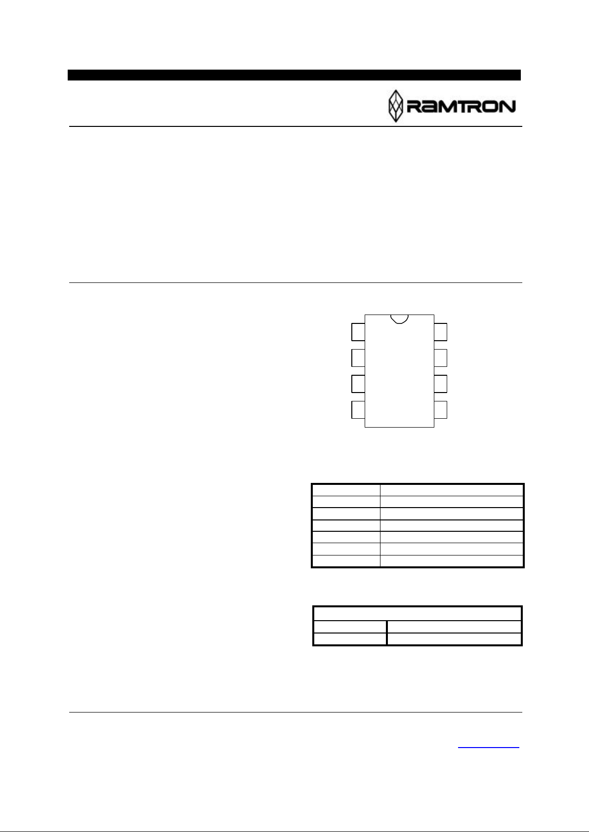
Pin Configuration
A0
A1
A2
VSS
VDD
WP
SCL
SDA
Pin Names Function
A0-A2 Device Select Address
SDA Serial Data/address
SCL Serial Clock
WP Write Protect
VSS Ground
VDD Supply Voltage 5V
Ordering Information
FM24C64-P 8-pin plastic DIP
FM24C64-S 8-pin SOP
Ramtron FM24C64
28 July 2000 2/13
Figure 1. FM24C64 Block Diagram
Address
Latch
`
1,024 x 64
FRAM Array
Data Latch
8
SDA
Counter
Serial to Parallel
Converter
Control Logic
SCL
WP
A0-A2
Pin Description
Pin Name Pin Number I/O Pin Description
A0-A2 1-3 I Address 0-2. These pins are used to select one of up to 8 devices of the
same type on the same two -wire bus. To select the device, the address
value on the three pins must match the corresponding bits contained in
the device address.
VSS 4 I Ground
SDA 5 I/O Serial Data Address. This is a bi-directional line for the two-wire
interface. It is open-drain and is intended to be wire-ORed with other
devices on the two-wire bus. The input buffer incorporates a schmitt
trigger for noise immunity and the output driver includes slope control
for falling edges. A pull-up resistor is required.
SCL 6 I Serial Clock. The serial clock line for the two-wire interface. Data is
clocked out of the part on the falling edge, and in on the rising edge. The
SCL input also incorporates a schmit trigger input for noise immunity.
WP 7 I Write Protect. When tied to VDD, addresses in the upper quadrant of the
logical memory map will be write-protected. Write access to the lower
three-quarters of the address area is permi tted. When WP is connected to
ground, all addresses may be written. This pin must not be left floating.
VDD 8 I Supply Voltage. 5V
Ramtron FM24C64
28 July 2000 3/13
Overview
The FM24C64 is a serial FRAM memory. The
memory array is logically organized as a 8,192 x 8 bit
memory array and is accessed using an industry
standard two-wire interface. Functional operation of
the FRAM is similar to serial EEPROMs. The major
difference between the FM24C64 and a serial
EEPROM with the same pin-out relates to its
superior write performance.
Memory Architecture
When accessing the FM24C64, the user addresses
8,192 locations each with 8 data bits. These data bits
are shifted serially. The 8,192 addresses are accessed
using the two-wire protocol, which includes a slave
address (to distinguish other non-memory devices),
and an extended 16-bit address. Only the lower 13
bits are used by the decoder for accessing the
memory. The upper three address bits should be set
to 0 for compatibility with larger devices in the
future.
The access time for memory operation is essentially
zero beyond the time needed for the serial protocol.
That is, the memory is read or written at the speed of
the two-wire bus. Unlike an EEPROM, it is not
necessary to poll the device for a ready condition
since writes occur at bus s peed. That is, by the time a
new bus transaction can be shifted into the part, a
write operation will be complete. This is explained in
more detail in the interface section below.
Users expect several obvious system benefits from
the FM24C64 due to its fast write cycle and high
endurance as compared with EEPROM. However
there are less obvious benefits as well. For example
in a high noise environment, the fast-write operation
is less susceptible to corruption than an EEPROM
since it is completed quickly. By contrast, an
EEPROM requiring milliseconds to write is
vulnerable to noise during much of the cycle.
Note that the FM24C64 contains no power
management circuits other than a simple internal
power-on reset. It is the user’s responsibility to
ensure that VDD is within data sheet tolerances to
prevent incorrect operation.
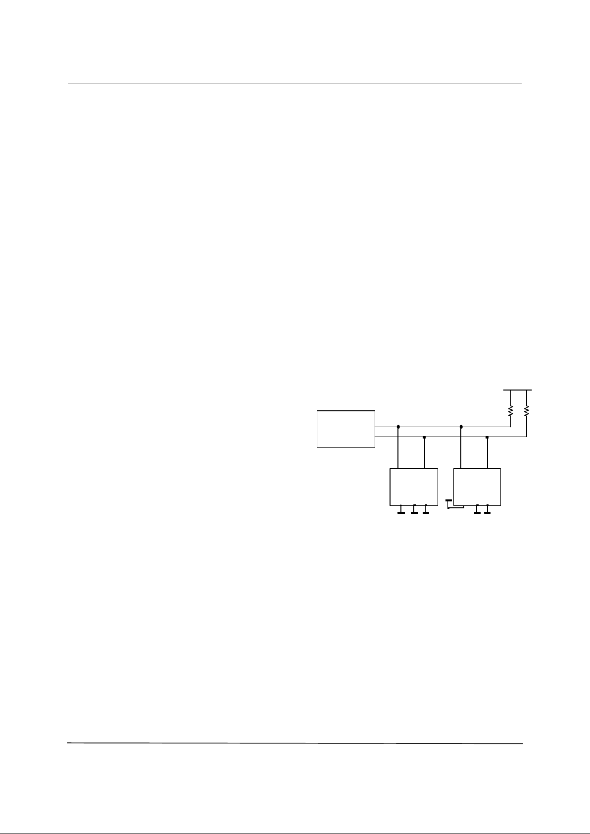
Two-wire Interface
The FM24C64 employs a bi-directional two -wire bus
protocol using few pins or board space. Figure 2
illustrates a typical system configuration using the
FM24C64 in a microcontroller-based system. The
industry standard two-wire bus is familiar to many
users but is described in this section.
By convention, any device that is sending data onto
the bus is the transmitter while the target device for
this data is the receiv er. The device that is controlling
the bus is the master. The master is responsible for
generating the clock signal for all operations. Any
device on the bus that is being controlled is a slave.
The FM24C64 always is a slave device.
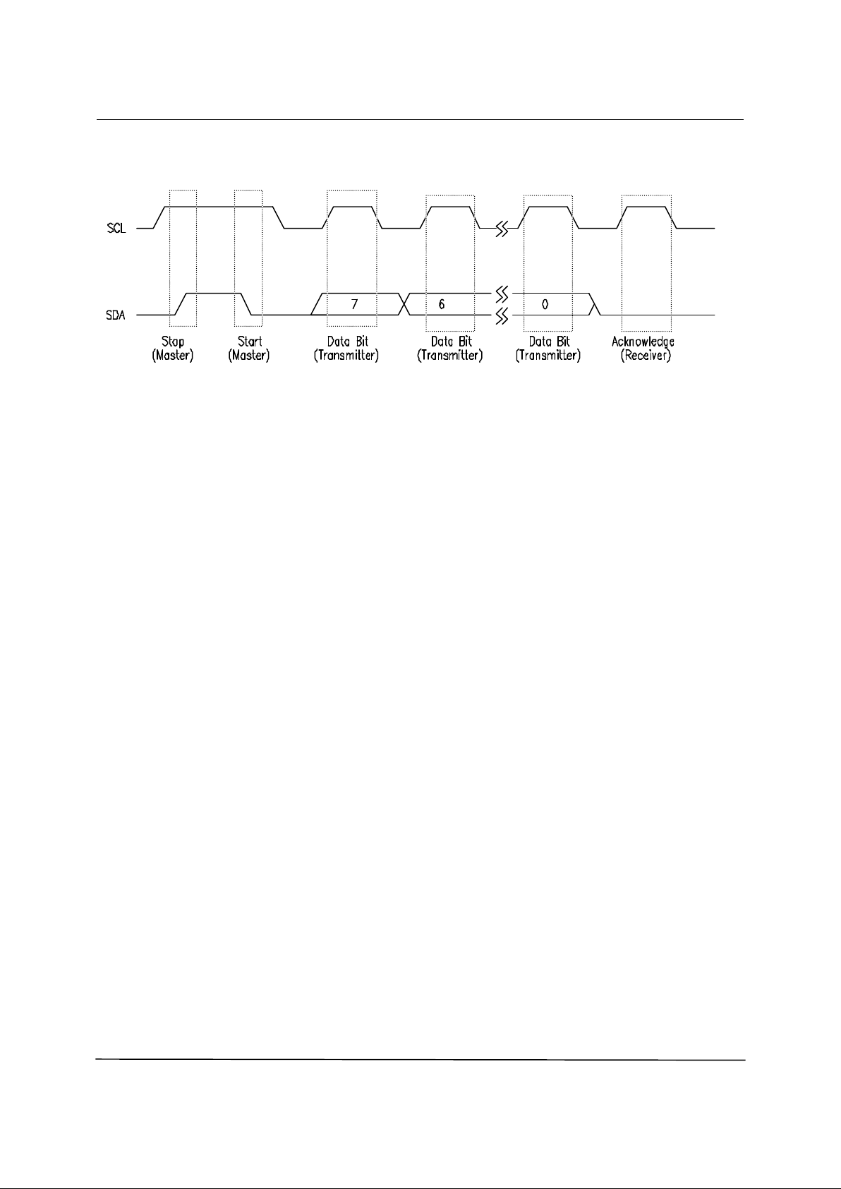
The bus protocol is controlled by transition states in
the SDA and SCL signals. There are four conditions
including start, stop, data bit, or acknowledge. Figure
3 illustrates the signal conditions that specify the four
states. Detailed timing diagrams are in the electrical
specifications.
Figure 2. Typical System Configuration
Microcontroller
SDA SCL
FM24C64
A0 A1 A2
SDA SCL
FM24C64
A0 A1 A2
VDD
Rmin = 1.8 K Ω
Rmax = tR/Cbus
Ramtron FM24C64
28 July 2000 4/13
Figure 3. Data Transfer Protocol
Start Condition
A start condition is indicated when the bus master
drives SDA from high to low while the SCL signal is
high. All commands should be preceded by a start
condition. An operation in progress can be aborted by
asserting a start condition at any time. Aborting an
operation using the start condition will ready the
FM24C64 for a new operation.
If during opera tion the power supply drops below the
specified VDD minimum, the system should issue a
start condition prior to performing another operation.
Stop Condition
A stop condition is indicated when the bus master
drives SDA from low to high while the SCL signal is
high. All operations using the FM24C64 should end
with a stop condition. If an operation is in progress
when a stop is asserted, the operation will be aborted.
The master must have control of SDA (not a memory
read) in order to assert a stop condition.
Data/Address Transfer
All data transfers (including addresses) take place
while the SCL signal is high. Except under the two
conditions described above, the SDA signal should
not change while SCL is high.
Acknowledge
The acknowledge takes place after the 8th data bit has
been transferred in any transaction. During this state
the transmitter should release the SDA bus to allow
the receiver to drive it. The receiver drives the SDA
signal low to acknowledge receipt of the byte. If the
receiver does not driv e SDA low, the condition is a
no-acknowledge and the operation is aborted.
The receiver would fail to acknowledge for two
distinct reasons. First is that a byte transfer fails. In
this case, the no-acknowledge ceases the current
operation so that the part can be addressed again.
This allows the last byte to be recovered in the event
of a communication error.
Second and most common, the receiver does not
acknowledge to deliberately end an operation. For
example, during a read operation, the FM24C64 will
continue to place data onto the bus as long as the
receiver sends acknowledges (and clocks). When a
read operation is complete and no more data is
needed, the receiver must not acknowledge the last
byte. If the receiver acknowledges the last byte, this
will cause the FM24C64 to attempt to drive the bus
on the next clock while the master is sending a new
command such as stop.
Slave Address
The first byte that the FM24C64 expects after a start
condition is the slave address. As shown in Figure 4,
the slave address contains the device type, the
device select address bits, and a bit that specifies if
the transaction is a read or a write.
Bits 7-4 are the device type and should be set to
1010b for the FM24C64. These bits allow other
types of function types to reside on the 2-wire bus
within an identical address range. Bits 3-1 are the
address select bits. They must match the
corresponding value on the external address pins to
select the device. Up to eight, FM24C64s can reside
on the same two-wire bus by assigning a different
address to each. Bit 0 is the read/write bit. A 0
indicates a write operation.
 Loading...