

RAMTRON FM1608-120-S, FM1608-120-P Datasheet
FM1608
64Kb Bytewide FRAM Memory
Features
64K bit Ferroelectric Nonvolatile RAM
• Organized as 8,192 x 8 bits
• High endurance 10 Billion (1010) read/writes
• 10 year data retention at 85° C
• NoDelay™ write
• Advanced high-reliability ferroelectric process
Superior to BBSRAM Modules
• No battery concerns
• Monolithic reliability
• True surface mount solution, no rework steps
• Superior for moisture, shock, and vibration
• Resistant to negative voltage undershoots
Description
The FM1608 is a 64-kilobit nonvolatile memory
employing an advanced ferroelectric process. A
ferroelectric random access memory or FRAM is
nonvolatile but operates in other respects as a RAM.
It provides data retention for 10 years while
eliminating the reliability concerns, functional
disadvantages and system design complexities of
battery -backed SRAM. Its fast write and high write
endurance make it superior to other types of
nonvolatile memory.
In-system operation of the FM1608 is very similar to
other RAM based devices. Memory read- and writecycles require equal times. The FRAM memory,
however, is nonvolatile due to its unique ferroelectric
memory process. Unlike BBSRAM, the FM1608 is a
truly monolithic nonvolatile memory. It provides the
same functional benefits of a fast write without the
serious disadvantages associated with modules and
batteries or hybrid memory solutions.
These capabilities make the FM1608 ideal for
nonvolatile memory applications requiring frequent or
rapid writes in a bytewide environment. The
availability of a true surface-mount package improves
the manufacturability of new designs, while the DIP
package facilitates simple design retrofits. The
FM1608 offers guaranteed operation over an
industrial temperature range of -40°C to +85°C.
SRAM & EEPROM Compatible
• JEDEC 8Kx8 SRAM & EEPROM pinout
• 120 ns access time
• 180 ns cycle time
• Equal access & cycle time for reads and writes
Low Power Operation
• 15 mA active current
• 20 µA standby current
Industry Standard Configuration
• Industrial temperature -40° C to +85° C
• 28-pin SOP or DIP
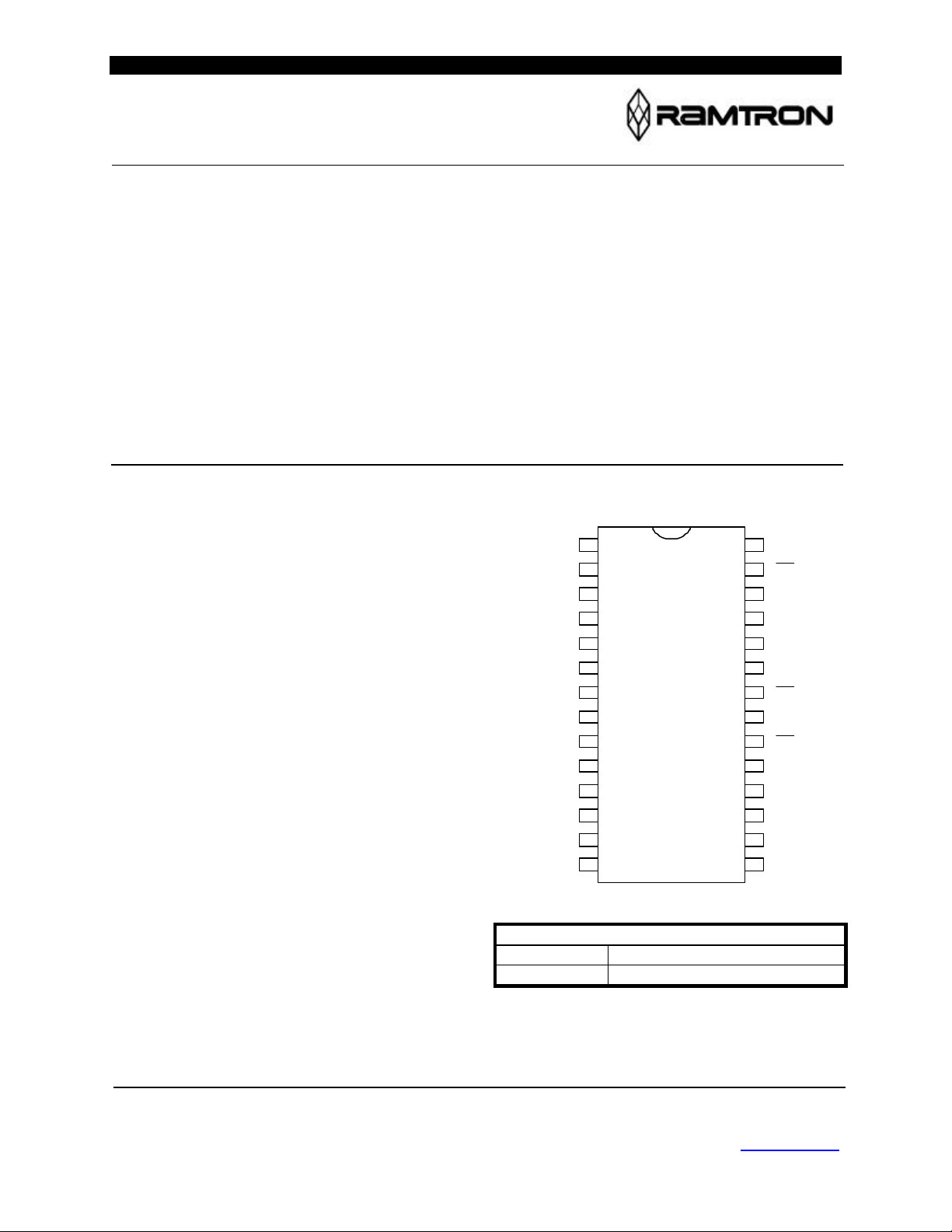
Pin Configuration
NC
A12
A7
A6
A5
A4
A3
A2
A1
A0
DQ0
DQ1
DQ2
VSS DQ3
VDD
WE
NC
A8
A9
A11
OE
A10
CE
DQ7
DQ6
DQ5
DQ4
Ordering Information
FM1608-120-P 120 ns access, 28-pin plastic DIP
FM1608-120-S 120 ns access, 28-pin SOP
This data sheet contains design specifications for product development. Ramtron International Corporation
These specifications may change in any manner without notice 1850 Ramtron Drive, Colorado Springs, CO 80921
(800) 545-FRAM, (719) 481-7000, Fax (719) 481-7058
www.ramtron.com
28 July 2000 1/12

Ramtron FM1608
Figure 1. Block Diagram
Pin Description
A10-A12
Block Decoder
CE
WE
OE
A0-A12
Address
Latch
Control
Logic
A0-A7
A8-A9
1Kx8
1Kx8
Row
Decoder
1Kx8
1Kx8
Column Decoder
I/O Latch
Bus Driver
1Kx8
1Kx8
1Kx8
1Kx8
DQ0-7
Pin Name Pin Number I/O Pin Description
A0-A12 2-10, 21, 23-25 I Address. The 13 address lines select one of 8,192 bytes in the FRAM
array. The address value will be latched on the falling edge of /CE.
DQ0-7 11-13, 15-19 I/O Data. 8-bit bi -directional data bus for accessing the FRAM array.
/CE 20 I Chip Enable. /CE selects the device when low. The falling edge of /CE
causes the address to be latched internally. Address changes that
occur after /CE goes low will be ignored until the next falling edge
occurs.
/OE 22 I Output Enable. When /OE is low the FM1608 drives the data bus when
valid data is available. Taking /OE high causes the DQ pins to be tri-
stated.
/WE 27 I Write Enable. Taking /WE low causes the FM1608 to write the contents
of the data bus to the address location latched by the falling edge of
/CE.
VDD 28 I Supply Voltage. 5V
VSS 14 I Ground.
Functional Truth Table
/CE /WE /OE Function
H X X Standby/Precharge
æ
X X Latch Address
L H L Read
L L X Write
28 July 2000 2/12

Ramtron FM1608
Overview
The FM1608 is a bytewide FRAM memory. The
memory array is logically organized as 8,192 x 8 and is
accessed using an industry standard parallel
interface. The FM1608 is inherently nonvolatile via its
unique ferroelectric process. All data written to the
part is immediately nonvolatile with no delay.
Functional operation of the FRAM memory is similar
to SRAM type devices. The major operating
difference between the FM1608 and an SRAM
(beside nonvolatile storage) is that the FM1608
latches the address on the falling edge of /CE.
Memory Architecture
Users access 8,192 memory locations each with 8 data
bits through a parallel interface. The complete address
of 13-bits specifies each of the 8,192 bytes uniquely.
Internally, the memory array is organized into 8 blocks
of 1Kb each. The 3 most-significant address lines
decode one of 8 blocks. This block segmentation has
no effect on operation, however the user may wish to
group data into blocks by its endurance requirements
as explained in a later section.
The access and cycle time are the same for read and
write memory operations. Writes occur immediately at
the end of the access with no delay. Unlike an
EEPROM, it is not necessary to poll the device for a
ready condition since writes occur at bus speed. A
pre-charge operation, where /CE goes inactive, is a
part of every memory cycle. Thus unlike SRAM, the
FM1608 access and cycle times are not equal.
Note that the FM1608 has no special power-down
demands. It will not block user access and it contains
no power-management circuits other than a simple
internal power-on reset. It is the user’s responsibility
to ensure that VDD is within data sheet tolerances to
prevent incorrect operation.
Memory Operation
The FM1608 is designed to operate in a manner very
similar to other bytewide memory products. For users
familiar with BBSRAM, the performance is comparable
but the bytewide interface operates in a slightly
different manner as described below. For users
familiar with EEPROM, the obvious differences result
from the higher write performance of FRAM
technology including NoDelay writes and much
higher write endurance.
Read Operation
A read operation begins on the falling edge of /CE. At
this time, the address bits are latched and a memory
28 July 2000 3/12
cycle is initiated. Once started, a complete memory
cycle must be completed internally regardless of the
state of /CE. Data becomes available on the bus after
the access time has been satisfied.
After the address has been latched, the address value
may change upon satisfying the hold time parameter.
Unlike an SRAM, changing address values will have
no effect on the memory operation after the address is
latched.
The FM1608 will drive the data bus when /OE is
asserted to a low state. If /OE is asserted after the
memory access time has been satisfied, the data bus
will be driven with valid data. If /OE is asserted prior
to completion of the memory access, the data bus will
not be driven until valid data is available. This feature
minimizes supply current in the system by eliminating
transients due to invalid data. When /OE is inactive
the data bus will remain tri-stated.
Write Operation
Writes occur in the FM1608 in the same time interval
as reads. The FM1608 supports both /CE and /WE
controlled write cycles. In all cases, the address is
latched on the falling edge of /CE.
In a /CE controlled write, the /WE signal is asserted
prior to beginning the memory cycle. That is, /WE is
low when /CE falls. In this case, the part begins the
memory cycle as a write. The FM1608 will not drive
the data bus regardless of the state of /OE.
In a /WE controlled write, the memory cycle begins on
the falling edge of /CE. The /WE signal falls after the
falling edge of /CE. Therefore the memory cycle
begins as a read. The data bus will be driven
according to the state of /OE until /WE falls. The
timing of both /CE and /WE controlled write cycles is
shown in the electrical specifications.
Write access to the array begins asynchronously
after the memory cycle is initiated. The write access
terminates on the rising edge of /WE or /CE,
whichever is first. Data set-up time, as shown in the
electrical specifications, indicates the interval during
which data cannot change prior to the end of the write
access.
Unlike other truly nonvolatile memory technologies,
there is no write delay with FRAM. Since the read and
write access times of the underlying memory are the
same, the user experiences no delay through the bus.
The entire memory operation occurs in a single bus

Ramtron FM1608
cycle. Therefore, any operation including read or write
can occur imme diately following a write. Data polling,
a technique used with EEPROMs to determine if a
write is complete, is unnecessary.
Pre-charge Operation
The pre-charge operation is an internal condition
where the state of the memory is prepared for a new
access. All memory cycles consist of a memory
access and a pre-charge. The pre-charge is user
initiated by taking the /CE signal high or inactive. It
must remain high for at least the minimum pre -charge
timing specification.
The user dictates the beginning of this operation
since a pre-charge will not begin until /CE rises.
However the device has a maximum /CE low time
specification that must be satisfied.
flexibility, the FM1608 employs a unique memory
organization as described below.
The memory array is divided into 8 blocks, each 1Kx8.
The 3-upper address lines decode the block selection
as shown in Figure 2. Data targeted for significantly
different numbers of cycles should be located in
separate blocks since memory rows do not extend
across block boundaries.
Figure 2. Address Blocks
Endurance and Memory Architecture
Data retention is specified in the electrical
specifications below. This section elaborates on the
relationship between data retention and endurance.
FRAM offers substantially higher write endurance
than other nonvolatile memories. Above a certain
level, however, the effect of increasing memory
accesses on FRAM produces an increase in the soft
error rate. There is a higher likelihood of data loss but
the memory continues to function properly. This
effect becomes significant only after 100 million (1E8)
read/write cycles, far more than allowed by other
nonvolatile memory technologies.
Endurance is a soft specification. Therefore, the user
may operate the device with different levels of cycling
for different portions of the memory. For example,
critical data needing the highest reliability level could
be stored in memory locations that receive
comparatively few cycles. Data with frequent changes
or shorter-term use could be located in an area
receiving many more cycles. A scratchpad area,
needing little if any retention can be cycled virtually
without limit.
Internally, a FRAM operates with a read and restore
mechanism similar to a DRAM. Therefore, each cycle,
be it read or write, involves a change of state. The
memory architecture is based on an array of rows and
columns. Each access causes an endurance cycle for
an entire row. Therefore, data locations targeted for
substantially differing numbers of cycles should not
be located within the same row. To balance the
endurance cycles and allow the user the maximum
Each block of 1Kx8 consists of 256 rows and 4
columns. The address lines A0-A7 decode row
selection and A8-A9 lines decode column selection.
This scheme facilitates a relatively uniform
distribution of cycles across the rows of a block. By
allowing the address LSBs to decode row selection,
the user avoids applying multiple cycles to the same
row when accessing sequential data. For example, 256
bytes can be accessed sequentially without accessing
the same row twice. In this example, one cycle would
be applied to each row. An entire block of 1Kx8 can
be read or written with only four cycles applied to
each row. Figure 3 illustrates the organization within a
memory block.
28 July 2000 4/12
 Loading...