

Page 1

20” TFT
SERVICE MANUAL
(17MB18)
Page 2

TABLE OF CONTENTS
1. SOFTWARE UPDATE DESCRIPTION .................................................................................................1
2. INTRODUCTION ...................................................................................................................................4
2.1. Scope .................................................................................................................................................4
2.2. General Features ...............................................................................................................................4
3. SYSTEM BUILDING BLOCKS ..............................................................................................................5
3.1. Analog Front End ...............................................................................................................................5
3.1.1. Tuner...........................................................................................................................................5
3.1.2. SAW Filters .................................................................................................................................6
3.2. Back End ............................................................................................................................................6
3.3. Side Board(s) .....................................................................................................................................9
3.3.1. Keypads......................................................................................................................................9
3.3.2. IR&Led Board .............................................................................................................................9
3.4. Power ...............................................................................................................................................10
4. IC AND COMPONENT DESCRIPTIONS ............................................................................................12
4.1. Basic IC List .....................................................................................................................................12
4.2. UOCIII ..............................................................................................................................................12
4.2.1. Pinout........................................................................................................................................13
4.3. PW1306 ...........................................................................................................................................17
4.3.1. Pinout........................................................................................................................................17
4.4. M29W800AT ....................................................................................................................................26
4.5. DS90C385........................................................................................................................................26
4.6. P15V330 ..........................................................................................................................................26
4.7. 74HC4052 ........................................................................................................................................26
4.8. TA1366FG........................................................................................................................................27
4.9. TDA7056A........................................................................................................................................27
4.10. TDA1308 ......................................................................................................................................27
4.11. LM1117.........................................................................................................................................28
4.12. 24LC32.........................................................................................................................................28
4.13. 24LC21.........................................................................................................................................28
4.14. 74LVC541.....................................................................................................................................29
4.15. SAA3010T ....................................................................................................................................29
4.16. MC34167 ......................................................................................................................................30
4.17. TFMS5360....................................................................................................................................30
4.18. Board Connectors, Headers & Jumpers.......................................................................................30
4.18.1. Analog PC Connector (PL400)..............................................................................................30
4.18.2. Scart Connector (PL401) ......................................................................................................31
4.18.3. S-Video Connector (JK403) ..................................................................................................31
4.18.4. LVDS Panel Connector(1x20 PL179) ...................................................................................31
4.18.5. TTL Panel Connector -Even (2x17 PL177)...........................................................................32
4.18.6. TTL Panel Connector -Odd (2x17 PL178) ............................................................................32
4.18.7. Panel Inverter Connector (1x11 PL176) ...............................................................................32
4.18.8. Keypad Card Connector (1x5 PL175)...................................................................................33
4.18.9. Optional Keypad Connector to UOC (1x2 PL 202) ...............................................................33
4.18.10. LED & IR Receiver Connector (1x6 PL202)..........................................................................33
4.18.11. Optional Rocker Sw. Connector (1x4 PL500) .......................................................................33
4.18.12. PROMJet Connector (2x25 PL101) ......................................................................................33
4.18.13. Side HP Connector for Side-card Option (PL405) ................................................................33
4.18.14. Side AV Connector for Side-card Option (PL406) ................................................................34
4.18.15. Side SVHS Connector for Side-card Option (PL407) ...........................................................34
5. DIGITAL MODULE IC and CONNECTOR DESCRIPTIONS ..............................................................35
5.1. STI5518............................................................................................................................................35
5.1.1. General Description................................................................................................................35
5.2. MAX232_SMD .................................................................................................................................35
5.2.1. General Description................................................................................................................35
5.2.2. Features ...................................................................................................................................35
5.3. 74HCU04 .........................................................................................................................................36
5.3.1. General Description................................................................................................................36
i
i
17” TFT TV Service Manual 19/11/2003
Page 3

5.3.2. Pin Description........................................................................................................................36
5.4. TSH22 ..............................................................................................................................................37
5.4.1. General Description................................................................................................................37
5.4.2. Pin Connections......................................................................................................................37
5.5. CS4334 ............................................................................................................................................37
5.5.1. General Description................................................................................................................37
5.5.2. Features ...................................................................................................................................37
5.6. AMIC A43L2616...............................................................................................................................38
5.6.1. General Description................................................................................................................38
5.6.2. Features ...................................................................................................................................38
5.6.3. Pin Description........................................................................................................................38
5.7. MX29LV160T ...................................................................................................................................40
5.7.1. General Description................................................................................................................40
5.7.2. Features ...................................................................................................................................40
5.7.3. Pin Description........................................................................................................................40
5.8. 24C32...............................................................................................................................................41
5.8.1. General Description................................................................................................................41
5.8.2. Features ...................................................................................................................................41
5.8.3. Pin Description........................................................................................................................41
5.9. STV0360 ..........................................................................................................................................42
5.9.1. General Description................................................................................................................42
5.9.2. Features ...................................................................................................................................42
5.9.3. Pin Description........................................................................................................................42
5.10. MAX809........................................................................................................................................45
5.10.1. General Description ............................................................................................................45
5.10.2. Features ...............................................................................................................................45
5.10.3. Pin Description....................................................................................................................45
5.11. TDCC2345TV39A.........................................................................................................................46
5.11.1. General Description ............................................................................................................46
5.11.2. Pin Description....................................................................................................................46
5.12. STV0700.......................................................................................................................................46
5.12.1. General description ............................................................................................................46
5.12.2. Features ...............................................................................................................................47
5.12.3. Pin Description....................................................................................................................47
5.13. 74HC373 ......................................................................................................................................52
5.13.1. General Description ............................................................................................................52
5.13.2. Pin Connections ..................................................................................................................52
5.14. 74HC245 ......................................................................................................................................52
5.14.1. General Description ............................................................................................................52
5.14.2. Features ...............................................................................................................................52
6. SERVICE MENU SETTINGS ..............................................................................................................53
6.1. UOCIII Service Menu .......................................................................................................................53
6.1.1. UOCIII Service Menu Settings ...............................................................................................53
6.1.2. Tuner AGC Alignment...............................................................................................................57
6.1.3. DCXO Alignment.......................................................................................................................57
6.2. PW1306 Service Menu ....................................................................................................................57
6.2.1. UOC Horizontal Position...........................................................................................................58
6.2.2. UOC Calibration........................................................................................................................58
6.2.3. PW1306 PC Input ADC Calibration ..........................................................................................58
6.2.4. Init NVM ....................................................................................................................................59
6.2.5. Initial APS .................................................................................................................................59
6.2.6. Hotel Mode Activate..................................................................................................................59
6.2.7. Burn-In Mode ............................................................................................................................59
6.2.8. Country .....................................................................................................................................59
6.2.9. Language ..................................................................................................................................59
6.2.10. Menu Background .................................................................................................................60
6.2.11. Remote Control .....................................................................................................................60
6.3. Panel Type Change Shortcut...........................................................................................................60
7. PRODUCTION SETTINGS AND FACTORY DEFAULTS...................................................................61
7.1. Production Schedule........................................................................................................................61
ii
ii
17” TFT TV Service Manual 19/11/2003
Page 4

7.2. EEPROM Settings............................................................................................................................61
7.2.1. Creating Master EEPROM........................................................................................................61
7.2.2. Creating Mass Production EEPROM ........................................................................................61
7.3. TV Menu...........................................................................................................................................61
7.3.1. Picture Menu.............................................................................................................................61
7.3.2. Audio Menu .............................................................................................................................61
7.3.3. Window Menu ...........................................................................................................................62
7.3.4. Options Menu............................................................................................................................62
7.3.5. Settings Menu ...........................................................................................................................62
7.4. PC Mode Menu ................................................................................................................................62
7.4.1. Picture Menu.............................................................................................................................62
7.4.2. Audio Menü...............................................................................................................................63
7.4.3. Window Menu ...........................................................................................................................63
7.4.4. Options Menü............................................................................................................................63
8. BLOCK DIAGRAM...............................................................................................................................65
9. CIRCUIT DIAGRAMS ..........................................................................................................................67
9.1. 17MB18-5 Main Board Schematics .................................................................................................67
9.2. Keypad Schematics .........................................................................................................................72
9.3. IR&LED Board Schematics ..............................................................................................................73
9.4. Remote Controller Schematics ........................................................................................................74
9.5. Digital Module Schematics...............................................................................................................75
9.6 Print Lay-outs(Analog Board)...........................................................................................................80
9.7 Print Lay-outs(Digital Board)............................................................................................................89
10. SPARE PART LIST .............................................................................................................................94
10.1 Analog Side Spare List......................................................................................................................94
10.2 Digital Side Spare List.....................................................................................................................108
11. Panel&Component Change List......................................................................................................109
iii
iii
17” TFT TV Service Manual 19/11/2003
Page 5

1. SOFTWARE UPDATE DESCRIPTION
1
1. IC Programming
17MB18 has two programmable ICs, UOCIII (IC203) and 29XX800 (IC102, having the
PW1306 (IC100) codes).
29XX800 (IC102) will be programmed before the TV production and will be mounted as
programmed. On the other hand, software update can be needed after production so the
programming instructions is given also for this IC in related chapter.
1.1. UOC III Programming
Step 1: Entering to ISP Mode
1. Press Power On and turn on the TV.
2. Press Remote Controls (RC) “Menu” (M) and “4””7””2””5” buttons respe ctively.
3. The following menu will displayed on the screen.
4. Press RCs “0” ”0” ”2” buttons respectively.(“ISP Mode 0” line will be displayed on the
screen.)
5. Press RCs “Volume +” button and set UOC to ISP mode. .(“ISP Mode 1” line will be
displayed on the screen.)
GTV 3.2.1
000 EurAsia TVSub 05.01
00000000 00111100
01000000 01100100
11000101 01100100
00000000 01100100
Step 2: Loading the Code
1- Connect the 5 pin cable of the “programming board” to PL203 of the 17MB18 mainboard.
Connect the programming board to the computer in which “WISP” program is loaded via
“Paralel Port”.
2- Run WISP program. As it is seen in figure1 change “Delay time” value to “5” ms.
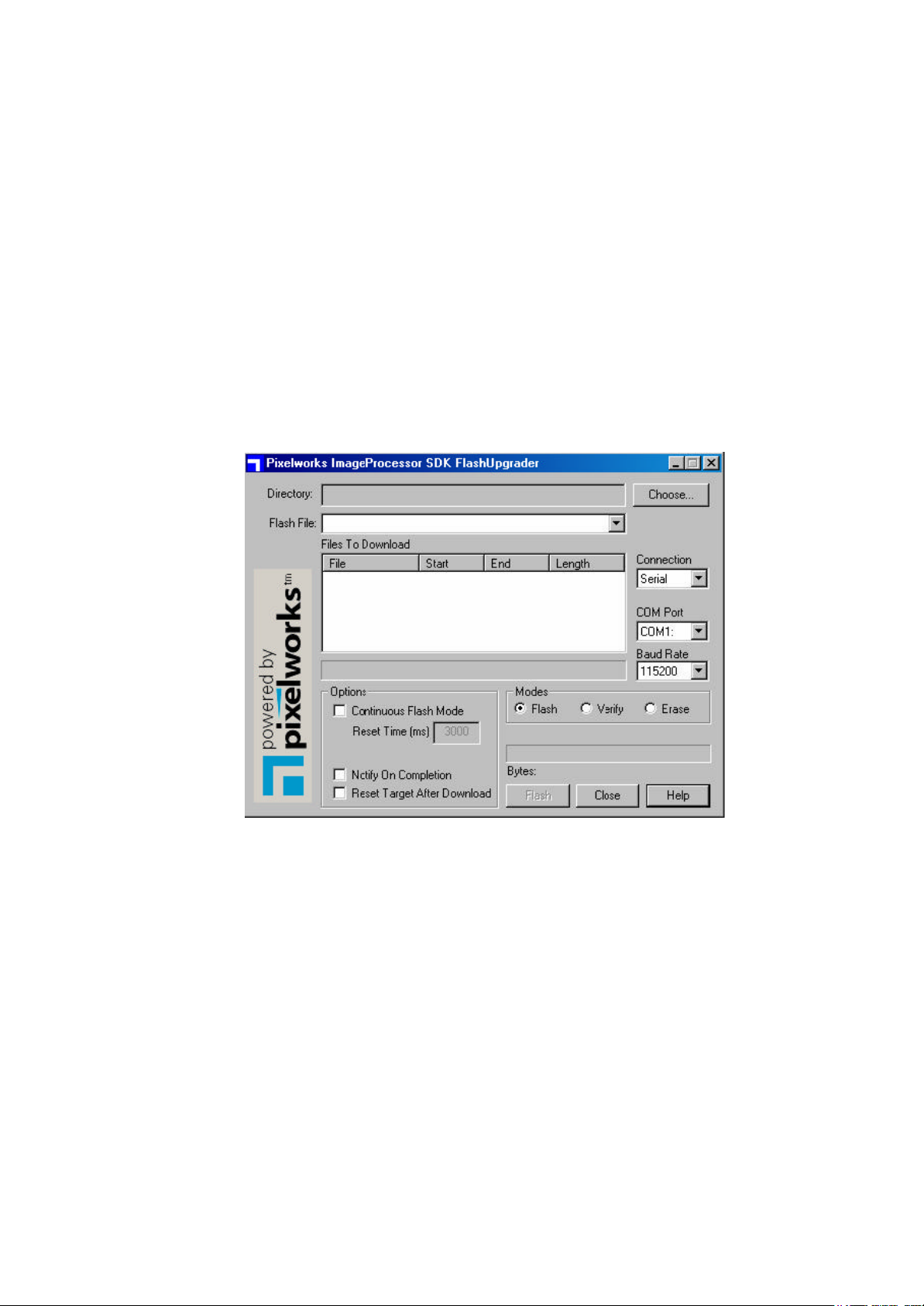
3- Under “Settings Menu”, set the I2C configurations as it is seen in figure2; press
“Confirm” and close this window.
(Note: Once the above settings are done, there is no need to do them again each time
loading the UOC code.)
4- Click “Enter ISP Mode” button and then click “Send” button. In the white display area
with “ISP status” heading, “ISP mode... Ready” will be displayed. (Unless you do not see
this warning, check the cable connections and the settings described above.)
Page 6
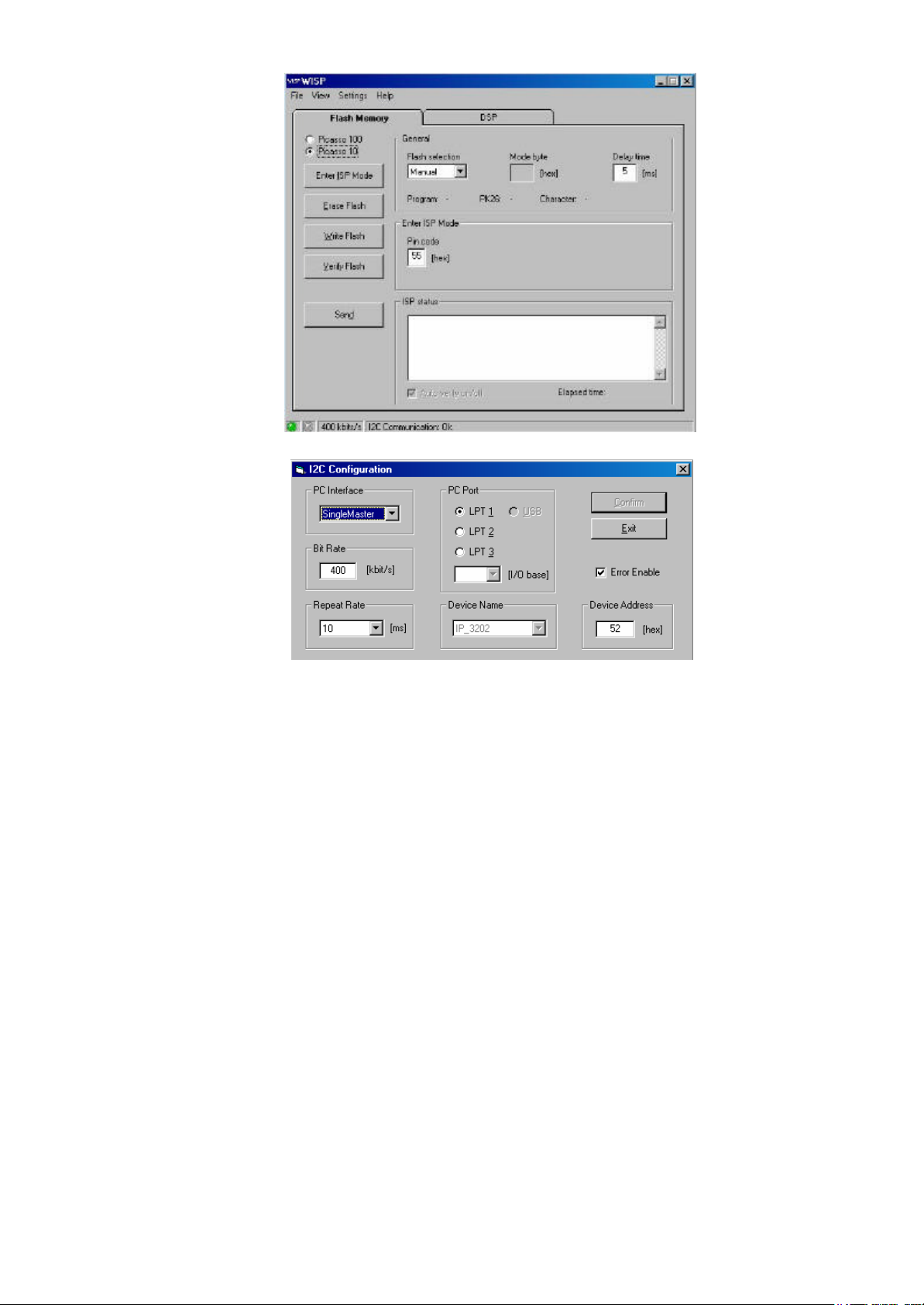
Figure1: WISP Main Menu
2
Figure2: I2C Configuration
5- Click “Erase Flash” button and then click “Send” button. If ereasing is done without any
problem, “three green OK” will be displayed on the main menu window. This indicates
that the memory inside the IC is erased succesfully.
6- Click “Write Flash” button and then click “Browse” button. Select the “gtv.hex” UOC code
file by browsing the explorer to the folder where this “gtv.hex” file is stored. Wait for a
few seconds untill the program reads the code. You will see the blue bar indicating the
“reading operation” on the bottom of the Wisp main menu window.
7- Click “Send” button. You will see the blue bar indicating the “Loading Code to UOC IC”
on the bottom of the window. When the loading operation is over without any error
“three green OK” will be displayed on the window. This indicates the loading operation is
performed succesfully.
Step3: Initializing the TV
8- Turn off and on the TV. Press RCs “Menu” (M) and “4””7””2””5” buttons respectively.
9- Press RCs “0” ”0” ”1” buttons respectively. (“Init TV 0” will be displayed on the screen)
10- Press RCs “Volume +” and set “Init TV 1” and wait the TV to automatically turn off.
Page 7
3
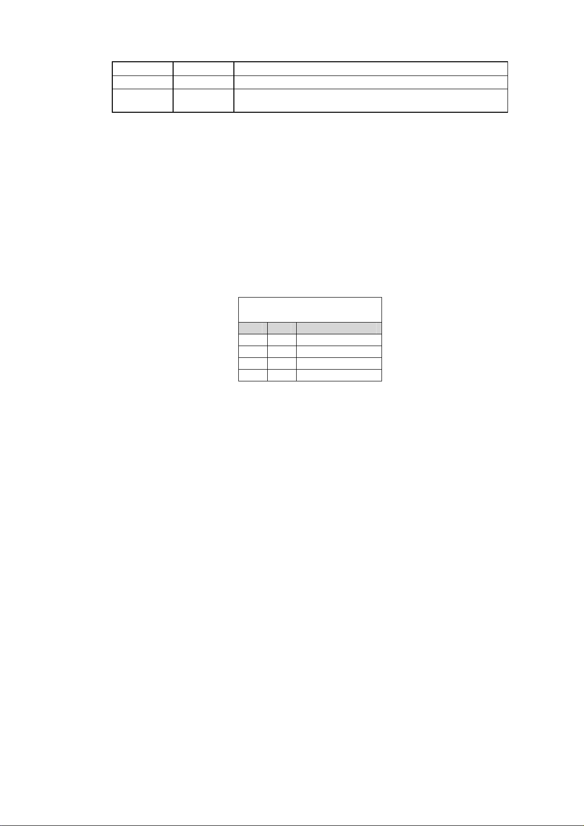
1.2. 29XX800 Programming for PW1306
The following instructions are only needed for software upgrades. For the TV production,
pre-programmed 29XX800 will be mounted on the board.
1- Copy flasher.hex and romcode.hex to “X:\XXX \ QTV_TVK2_V_021\Project\PW13XX_QTV”
directory.
2- Connect programmer board 4-pin cable to PL100 on 17MB18.
3- Connect programmer board serial port cable to PC COM Port1.
4- Close jumper PL501.
5- Execute “FlashUpgrader.exe” in “C:\XXX\ QTV_TVK2_V_021\bin\” directory.
6- Press “Choose” and select romcode.inf from
“C:\XXX\ QTV_TVK2_V_021\Project\PW13XX_QTV” directory.
7- Press “Flash”
8- Power on the board. Observe the sliding bar on the main menu showing that flasher.hex
and then romcode.hex are being downloaded to the IC on 17MB18 main board.
9- Power off the board when the download operation is over.
10- Open jumper PL501.
11- Power On the board. Press Remote Controls (RC) “Menu” (M) and “4””7””2””6” buttons
respectively.
12- By using RIGHT and LEFT buttons of the RC, select “Service Submenu 2”
13- By using DOWN button of the RC highlight Init NVM. Press RIGHT button of the RC and
initialize the PixelWorks side.
14- Turn Off and On the TV.
15- Depanding the size of the Panel(15”, 17”, 20”) the screen may be full white and no
picture is observed.
If screen is full white:
For 15” TV, Press Remote Controls (RC) “Menu” (M) and “4” “7” “2” “6” buttons and then “0”
respectively.
For 17” TV, Press Remote Controls (RC) “Menu” (M) and “4” “7” “2” “6” buttons and then “2”
respectively.
For 20” TV, Press Remote Controls (RC) “Menu” (M) and “4” “7” “2” “6” buttons and then “1”
respectively.
Page 8

2. INTRODUCTION
2.1. Scope
The document covers 20” integrated digital TV(IDTV) 17MB18 chassis building blocks, basic features, service menu
settings, and the other information needed by service personal.
2.2. General Features
The system is a 14” to 23” TFT LCD TV solution with UOCIII Versatile Signal Processor and PW1306 Video Image
Processor chip-set on 4-layer PCB. The TV will support PAL/SECAM B/G/D/K/I/L/L’.
The other general default features of the TV are as listed below:
1 Full Scart input (with SVHS support)
1 SVHS input through standard S-Video interface.
1 CVBS input through standard RCA jack
75 ohms antenna input
D-Sub 15 PC Input
GERMAN + NICAM STEREO
<3W S/B Power Consumption from mains supply
2x3W Speaker Output Power @16 Ohm spks; HP Output, Stereo Audio line out
Stereo Audio line in
Equalizer
IR Control (RC5)
OSD;Menu Languages ENG, FRA, GER, ITA, SPA, POR, TUR, SWE, DEN, FIN, CRO, SLO, SLOVEN, NOR,
POL, CZE, HUN,ROM,BUL, RUS (subject to change and be grouped)
Teletext
2H/4H Comb Filter
White balance settings (warm/normal/cool) for TV&PC
Full AIR&CABLE band coverage
Auto Shut down
4
4
17” TFT TV Service Manual 19/11/2003
Page 9

3. SYSTEM BUILDING BLOCKS
17MB18 chassis main blocks are as follows:
Analog Front End : UOCIII (Microcontroller + Video Proccessor + Sound Proccessor + IF), CTI, Tuner, SAW
filters, Audio Amp., DAC
Back End : PW1306(Microcontroller, Scaler, OSD, Keyboard/IR Interface)
Side Board(s) : Keyboards, IR/LED Boards, TTL Panel Interface Cards, VCbCr Input Board (Optional)
3.1. Analog Front End
17MB18 Main Board consists of two major blocks. The first block is analog front-end and this block is handled by
UOCIII chip that is highly multifunctional. This IC does demodulation of Video & Audio from Tuner IF, CVBS, Audio,
RGB, SVHS input selection and processing. It has an audio processor that supports equalizer or tone control, volume
control, AVL, surround effect etc and supplies amplifier, headphone and CVBS & audio line outputs. It handles video
processing such as colour standard detection and demodulation, picture alignment (brightness, contrast, colour etc.). The
IC also does teletext decoding with 10 pages text memory. After video processing, the processed video is applied to
PW1306 chip in RGB format.
The TV Tuner is an asymmetrical IF output type and is PLL controlled. For multistandard reception, a switchable SAW
filter is used as the sound filter and it is controlled by SAW_SW output from UOC. After the SAW filter block, IF signal
is applied to UOC IF inputs (VIFIN[1,2] and SIF[1,2]).
As UOCIII can handle all the audio processing, there is no need for additional audio processor solution on the board.
UOC supports three Audio outputs. These outputs are assigned to Headphone, Speaker and Scart Audio line outputs. The
board employs TDA7056A and TDA1308 to drive speaker and headphone outputs respectively. As another dedicated
output for Audio Line out from jack is not possible in UOC, this line out signal is obtained by using I2S input DAC
CS4335. UOCIII I2S output is converted to anolog signal by DAC CS4335.
3.1.1.Tuner
As the thickness of the TV set has a limit, a horizontal mounted tuner with longer connector is used in the
product. The tuning is available through the digitally controlled I2C bus (PLL). Below you will find info on the
Asymmetrical Tuner in use.
General description:
The tuner meets a wide range of applications. It is a combined VHF, UHF tuner suitable for CCIR systems
B/G, H, L, L’, I and I’. The low IF output impedance drives a wide variety of SAW filters with sufficient
suppression of triple transient.
Features:
Small sized UHF/VHF tuners
Systems CCIR: B/G, H, L, L’, I and I’; OIRT: D/K
Digitally controlled (PLL) tuning via I2C-bus
Off-air channels, S-cable channels and Hyper band
ZS(AE) Aerial source impedance (unbalanced) 75 Ohm
PIN SYMBOL DESCRIPTION
1
2
3
4
5
6
7
8
9
AGC
Automatic Gain Control Voltage 4 0.1
TU Tuning voltage monitor (output)
AS
SCL
SDA
I 2C-Bus Address Select
I 2C-Bus Serial Clock
I 2C-Bus Serial Data
n.c. Not Connected
Vs
ADC
VST
Supply Voltage +5V 0.125
ADC Input
Fixed tuning Supply Voltage +33V 0.5
Page 10
10
11
M1,M2,M3,
M4
3.1.2. SAW Filters
K3953M is an IF Filter for Video Applications. The package is SIP5K. Supported standards are B/G, D/K, I,
L/L’.
K9656M is an IF Filter for Audio Applications. The package is SIP5K. Supported standards are B/G, D/K, I,
L/L’.
3.2. Back End
The Back End section is handled by PW1306 chip. This IC has built in ADC’s for RGB and SOY support. The RGB input
can handle standard interlaced RGB output from UOC, PC VGA RGB input. As only 1 set of ADC is present in PW1306
these sources should be multiplexed.
All the multiplexing operations are controlled by PW1306 via YUV_TV_SW (58) and VGA_TV_SW (57) signals.
The video output from PW1306 is a 48-bit digital RGB bus format and made available on two separate connectors with
TTL control signals (i.e. HS, VS, CLK, etc.). This digital output is intended to interface to TTL compatible display
devices. As PW1306 does not have integrated LVDS transmitter, 24 bit (even part of RGB) video output and TTL control
signals from PW1306 are also inputted to DS90C385 LVDS IC to produce single pixel LVDS output for LVDS
compatible LCDs.
Backlight control is also possible via PW1306 Porta7 pin (PWMOUT, PL176-10), that is a variable duty-cycle pulse
generator output.
I.F out 2 Symmetrical I.F output 2 / Do not connect for asymmetrical
I.F out 1 Asymmetrical I.F Output / Symmetrical I.F output 1
GND Mounting Tags (Ground)
A: VGA _TV_SW
B: YUV _TV_SW
A B SYNC SOURCE
0 0 UOC
0 1 VGA
1 0 YcbCr
1 1 NOT USED
Table 2: H/V Sync Multiplexing Table
6
6
17” TFT TV Service Manual 19/11/2003
Page 11
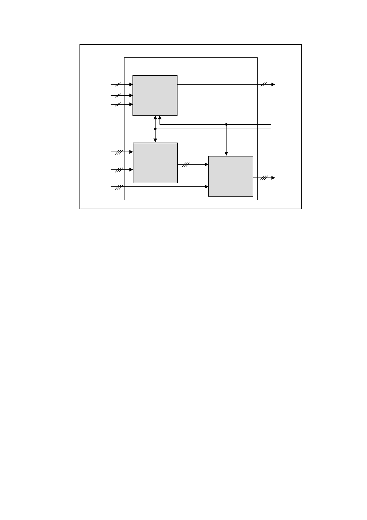
MUX BLOCK
V[R,G,B]IN
YCbCr
[R,G,B]OUT
RGB
TV_[HS,VS]
PC_[HS,VS]
HD_[HS,VS]
MUX
74HC4052D
VIDEO
SWITCH
P15V330
Figure 1: MUX Block.
AHSYNC
AVSYNC
Control Signals:
VGA_TV_SW
YUV_TV_SW
TV_[R,G,B]AIN
VIDEO
SWITCH
P15V330
7
7
17” TFT TV Service Manual 19/11/2003
Page 12
SAW
RF in
MACROVISION
S-Video in
CVBS in
Scart
TV_HS
TV_VS
VFIN (24,25)
UOCIII
Y4(51)
C4(52)
CVBS3/Y3(58) IDTV RGB(70,71,72)
AUDIOIN5L(34) IDTV R/L(54,55)
AUDIOIN5R(35)
C2(59)
CVBS2/Y2(55)
IFVO(43)
AUDIOUTSL(36)
AUDIOUTSR(37)
AUDIOIN3L(56)
AUDIOIN3R(57)
VDRA,HOUT(23,67)
16MB39
IDTV Module
Audio in
[R,G,B]IN
PC in
Y HD_[HS,VS]
SYNC
SEPARATOR
EL1883
PC_[HS,VS]
CTI/
LTI
MUX
BLOCK
[YUV,VGA]_SW
A[H,V]SYNC
FBLIN
AUDOUTHP[L,R](62,63)
R,G,B(78,79,80)
[Y,U,V]OUT(74,75,76)
AUDOUTLS[L,R](60,61)
YUV(72,71,70)
I2SDO2(104)
I2SCLK(103)
I2SWS(102)
[R,G,B]OUT(85,86,87)
Comunication
Signals:
I2C and Handhake
PORTD[5,6](58,57)
SDA_U, SCL_U
PW1306
[H,V]SYNC(65,64)
[R,G,B]AIN(37,43,50)
PORTD7(56)
Communication Interface UART: Rx,Tx, Up-IRQ
D[R,G,B]E[0-7], PORTA7(201)
DHS,DVS,DEN,DCLK D[R,G,B]O[0-7]
HP DRIVER
TDA1308
AUDIO
AMPLIFIER
2xTDA7056
DAC
Audio
line out
EEPROM
16MB39 IDTV
LVDS
DS90C385
Figure 2: TV system block diagram.
8
8
17” TFT TV Service Manual 19/11/2003
Page 13
3.3. Side Board(s)
3.3.1. Keypads
The keypads (17TK15, 16, 17, 20, 21, 26) for 17MB18 main board are listed in the Table below. (They have the same
connector pinning though):
20”
Key Name Type Function 21
Power Soft sw. Power shut-down and turn on X
Stand-by Tact sw. Switch between stand-by and turn on modes. TV/AV Tact sw. Input source select button. X
Menu Tact sw. Display main menu on the screen. If any menu is
active, display the upper menu. If main menu is
active, turn menu off.
Program- Tact sw. Go to the lower program at any time in TV mode.
In menu mode, go to down menu item.
Program+ Tact sw. Go to the upper program at any time in TV mode.
In menu mode, go to up menu item.
Volume- Tact sw. Decrease the volume level in the volume. In menu
mode, go to left menu item.
Volume+ Tact sw. Increase the volume level in the volume. In menu
mode, go to right menu item.
Connector PL1 on keypads (connected to the connector PL175 on the main board):
X
X
X
X
X
Pin No: Name Pin No: Name:
1 Volume+ 6 Program+
2 Volume- 7 Program3 Ground 8 Menu
4 Not Connected* 9 TV/AV
5 Ground 10 Stand-by/Shut-down
*Reserved: It can be +5V in the future designs if needed.
3.3.2. IR&Led Board
IR&LED board contains LED indicator(s) to show TV’s status (Red for stand-by, green for normal operation) and one IR
receiver to get remote control instructions. All the IR&LED boards have the same circuit and connector pinning but the
different mechanical structure to fit different cabinets (see the related section for schematics and connector pinning).
17” TFT TV Service Manual
9
Page 14
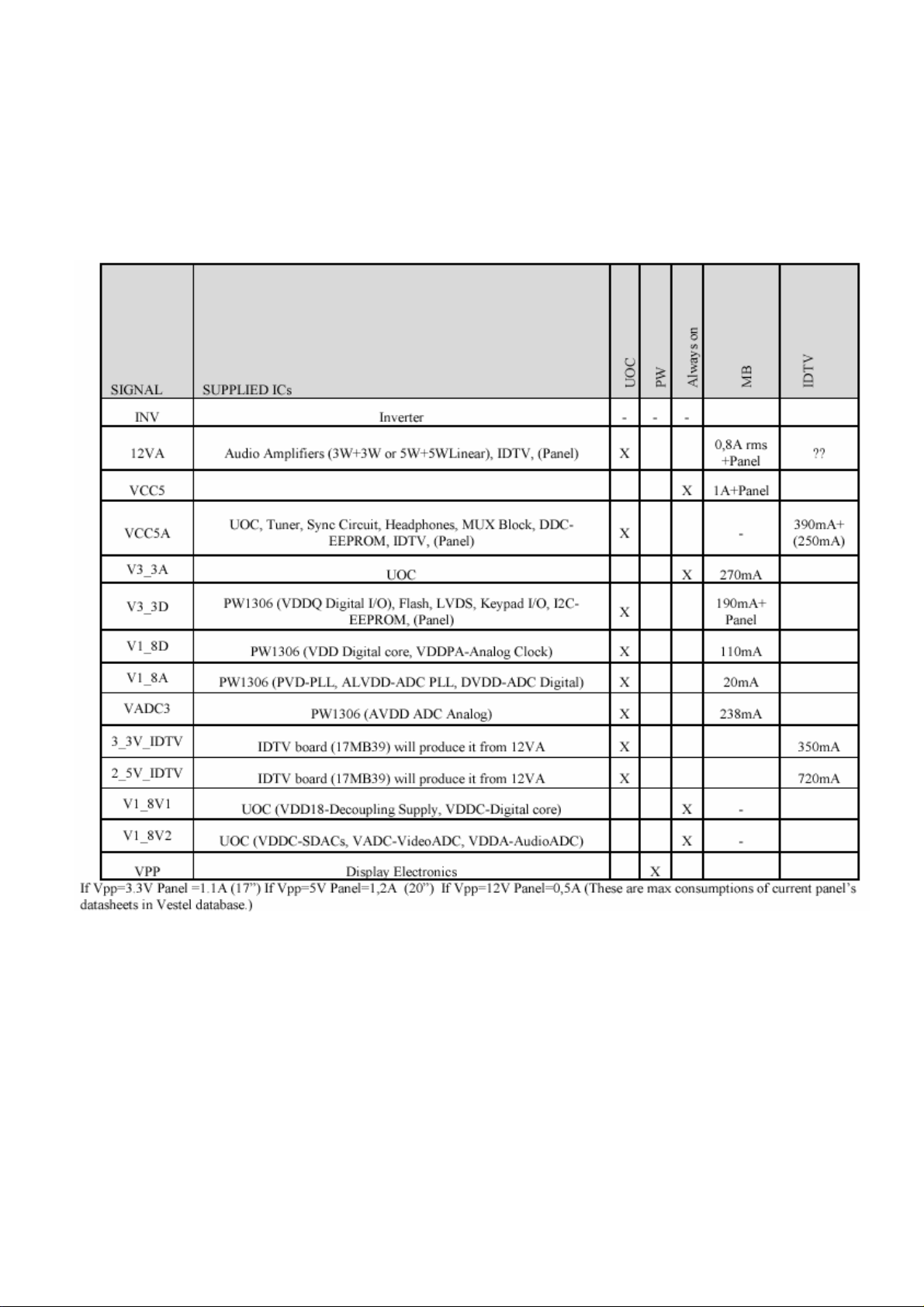
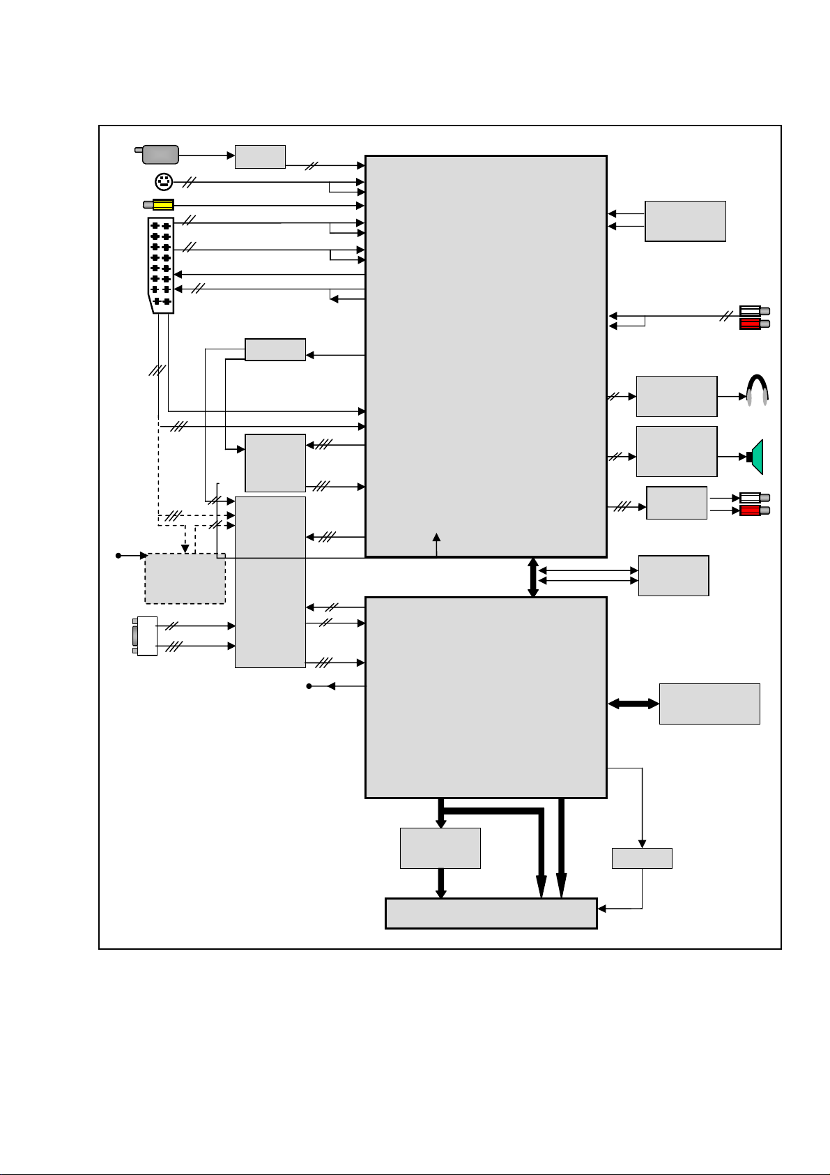
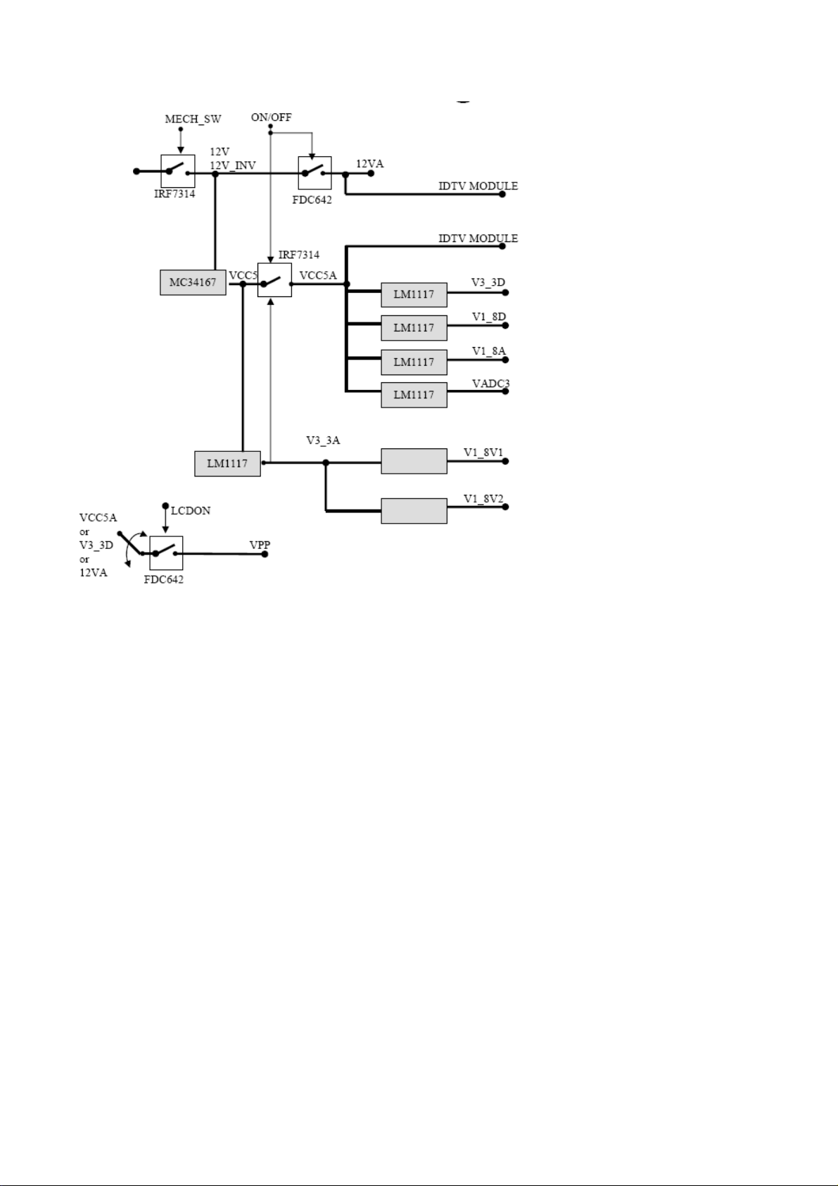
3.4. Power
Several linear regulators and switches are used to generate several separate analog and digital voltage supplies such as +5, +3.3,
+1.8, etc. (Please check the Figure 3, and Table 3 for power management details.)
17” TFT TV Service Manual
Table 3: Power management table.
10
Page 15
17” TFT TV Service Manual
11
Page 16
4. IC AND COMPONENT DESCRIPTIONS
4.1. Basic IC List
No Title Description
IC203 UOCIII Versatile Signal Processor
IC100 PW1306 Video Image Processor with Analog Interface
IC102 MT28F800B3W Flash Memory
IC176 DS90C385 Programmable LVDS Transmitter
IC103 EL1883 Sync Separator
IC405, IC402 P15V330 Wide Bandwidth 2-channel Multiplexer/Demultiplexer
IC404 74HC4052 Dual 4-channel Analog Multiplexer
IC200 TA1366FG LTI/CTI IC
IC410, IC411 TDA7056A Class AB Mono 3W Power Amplifier
IC401 TDA1308 Class AB Stereo Headphone Driver
IC500/1/2/3/4,
LM1117 Linear Regulator
IC201
IC400 24LC21
IC101 24LC32
Serial Electrically Erasable PROM
4.2. UOCIII
The UOCIII series combines the functions of a Video Signal Processor (VSP) together with a FLASH embedded
TEXT/Control/Graphics m-Controller (TCG m-Controller) and US Closed Caption decoder. In addition the following functions
can be added:
Adaptive digital (4H/2H) PAL/NTSC combfilter
Teletext decoder with 10 page text memory
Multi-standard stereo decoder
BTSC stereo decoder
Digital sound processing circuit
Digital video processing circuit
The UOC III series consists of the following 3 basic concepts:
Stereo versions. These versions contain the TV processor with a stereo audio selector, the TCG m-Controller, the multi-
standard stereo or BTSC decoder, the digital sound processing circuit and the digital video processing circuit. Options are
the adaptive digital PAL/NTSC comb filter and a teletext decoder with 10 page text memory.
AV stereo versions. These versions contain the TV processor with stereo audio selector and the TCG m-Controller. Options
are the digital sound processing circuit, the digital video processing circuit, the adaptive digital PAL/NTSC comb filter and
a teletext decoder with a 10 page text memory.
Mono sound versions. These versions contain the TV processor with a selector for mono audio signals and the TCG m-
Controller. Options are the adaptive digital PAL/NTSC combfilter and a teletext decoder with 10 page text memory.
17” TFT TV Service Manual
12
Page 17
4.2.1. Pinout
Figure 6: UOCIII Pin configuration “stereo” and “AV-stereo” versions with Audio DSP
SYMBOL
VSSP2 1 1 1 ground
VSSC4 2 2 2 ground
VDDC4 3 3 3 digital supply to SDACs (1.8V)
VDDA3(3.3V) 4 4 4 supply (3.3 V)
VREF_POS_LSL 5
VREF_NEG_LSL+HPL 6
VREF_POS_LSR+HPR 7
STEREO +AV
STEREO
AV STEREO
NO AUDIO
DSP
- -
- -
- -
MONO DESCRIPTION
positive reference voltage SDAC (3.3 V)
negative reference voltage SDAC (0 V)
positive reference voltage SDAC (3.3 V)
13
17” TFT TV Service Manual
Page 18

SYMBOL
STEREO +AV
STEREO
VREF_NEG_HPL+HPR 8
VREF_POS_HPR 9
AV STEREO
NO AUDIO
DSP
- -
- -
MONO DESCRIPTION
negative reference voltage SDAC (0 V)
positive reference voltage SDAC (3.3 V)
XTALIN 10 10 10 crystal oscillator input
XTALOUT 11 11 11 crystal oscillator output
VSSA1 12 12 12 ground
VGUARD/SWIO 13 13 13
V-guard input / I/O switch (e.g. 4 mA current
sinking capability for direct drive of LEDs)
DECDIG 14 14 14 decoupling digital supply
VP1 15 15 15
1stsupply voltage TV-processor (+5 V)
PH2LF 16 16 16 phase-2 filter
PH1LF 17 17 17 phase-1 filter
GND1 18 18 18 ground 1 for TV-processor
SECPLL 19 19 19 SECAM PLL decoupling
DECBG 20 20 20 bandgap decoupling
EWD/AVL (1)
21 21 21 East-West drive output or AVL capacitor
VDRB 22 22 22 vertical drive B output
VDRA 23 23 23 vertical drive A output
VIFIN1 24 24 24 IF input 1
VIFIN2 25 25 25 IF input 2
VSC 26 26 26 vertical sawtooth capacitor
IREF 27 27 27 reference current input
GNDIF 28 28 28 ground connection for IF amplifier
SIFIN1/DVBIN1 (2)
SIFIN2/DVBIN2 (2)
29 29 29 SIF input 1 / DVB input 1
30 30 30 SIF input 2 / DVB input 2
AGCOUT 31 31 31 tuner AGC output
EHTO 32 32 32 EHT/overvoltage protection input
AVL/SWO/SSIF/
REFO/REFIN (2)(3)
33 33 33 Automatic Volume Levelling / switch output /
sound IF input / subcarrier reference output /
external reference signal input for I signal mixer for
DVB operation
AUDIOIN5
AUDIOIN5L 34 34
- -
34 audio 5 input
-
audio-5 input (left signal)
AUDIOIN5R 35 35 - audio-5 input (right signal)
AUDOUTSL 36 36
-
audio output for SCART/CINCH (left signal)
AUDOUTSR 37 37 - audio output for SCART/CINCH (right signal)
DECSDEM 38 38 38 decoupling sound demodulator
QSSO/AMOUT/AUDEEM
(2)
39 39 39
QSS intercarrier output / AM output / deemphasis
(front-end audio out)
GND2 40 40 40 ground 2 for TV processor
PLLIF 41 41 41 IF-PLL loop filter
14
17” TFT TV Service Manual
Page 19

SYMBOL
SIFAGC/DVBAGC (2)
DVBO/IFVO/FMRO (2)
DVBO/FMRO (2) 44 44 - Digital Video Broadcast output / FM radio output
VCC8V 45 45 45 8 Volt supply for audio switches
AGC2SIF 46
VP2 47 47 47
IFVO/SVO/CVBSI (2)
AUDIOIN4
AUDIOIN4L 49 49
AUDIOIN4R 50 50 - audio-4 input (right signal)
CVBS4/Y4 51 51 51 CVBS4/Y4 input
C4 52 52 52 chroma-4 input
AUDIOIN2
AUDIOIN2L/SSIF (3)
AUDIOIN2R 54 54 - audio 2 input (right signal)
STEREO +AV
STEREO
42 42 42
43 43 43
48 48 48
- -
- -
53 53
AV STEREO
NO AUDIO
DSP
- -
MONO DESCRIPTION
AGC sound IF / internal-external AGC for DVB
applications
Digital Video Broadcast output / IF video output /
FM radio output
AGC capacitor second sound IF
2ndsupply voltage TV processor (+5 V)
IF video output / selected CVBS output / CVBS
input
49 audio 4 input
-
audio-4 input (left signal)
53 audio 2 input
-
audio 2 input (left signal) / sound IF input
CVBS2/Y2 55 55 55 CVBS2/Y2 input
AUDIOIN3 - - 56 audio 3 input
AUDIOIN3L 56 56
AUDIOIN3R 57 57 - audio 3 input (right signal)
CVBS3/Y3 58 58 58 CVBS3/Y3 input
C2/C3 59 59 59 chroma-2/3 input
AUDOUTLSL 60 62
AUDOUTLSR 61 63
AUDOUT/AMOUT/FMOU
T
AUDOUTHPL 62 - - audio output for headphone channel (left signal)
AUDOUTHPR 63
CVBSO/PIP 64 64 64 CVBS / PIP output
SVM 65 65 65 scan velocity modulation output
FBISO/CSY 66 66 66
HOUT 67 67 67 horizontal output
VSScomb 68 68 68 ground connection for comb filter
VDDcomb 69 69 69 supply voltage for comb filter (5 V)
- -
- -
-
audio 3 input (left signal)
-
audio output for audio power amplifier (left signal)
- audio output for audio power amplifier (right
signal)
62
audio output / AM output / FM output, volume
controlled
audio output for headphone channel (right signal)
flyback input/sandcastle output or composite H/V
timing output
VIN (R/PRIN2/CX) 70 70 70
UIN (B/PBIN2) 71 71 71
YIN (G/YIN2/CVBS-YX) 72 72 72
YSYNC 73 73 73 Y-input for sync separator
V-input for YUV interface (2ndR input / PRinput or
CXinput)
U-input for YUV interface (2ndB input / PB input)
Y-input for YUV interface (2nd G input / Y input or
CVBS/YXinput))
15
17” TFT TV Service Manual
Page 20

SYMBOL
YOUT 74 74 74 Y-output (for YUV interface)
UOUT (INSSW2) 75 75 75
VOUT (SWO1) 76 76 76 V-output for YUV interface (general purpose
INSSW3 77 77 77
R/PRIN3 78 78 78
G/YIN3 79 79 79
B/PBIN3 80 80 80
GND3 81 81 81 ground 3 for TV-processor
VP3 82 82 82
BCLIN 83 83 83 beam current limiter input
BLKIN 84 84 84 black current input
RO 85 85 85 Red output
GO 86 86 86 Green output
BO 87 87 87 Blue output
VDDA1 88 88 88 analog supply for TCG m-Controller and digital
STEREO +AV
STEREO
AV STEREO
NO AUDIO
DSP
MONO DESCRIPTION
U-output for YUV interface (2ndRGB / YPBPR
insertion input)
switch output)
3rdRGB / YPBPR insertion input
3rdR input / PRinput
3rdG input / Y input
3rdB input / PBinput
3rdsupply for TV processor
supply for TV-processor (+3.3 V)
VREFAD_NEG 89 89 89 negative reference voltage (0 V)
VREFAD_POS 90 90 90 positive reference voltage (3.3 V)
VREFAD 91
GNDA 92 92 92 ground
VDDA(1.8V) 93 93 93 analogue supply for audio ADCs (1.8 V)
VDDA2(3.3) 94 94 94 supply voltage SDAC (3.3 V)
VSSadc 95 95 95 ground for video ADC and PLL
VDDadc(1.8) 96 96 96 supply voltage video ADC and PLL
INT0/P0.5 97 97 97
P1.0/INT1 98 98 98 port 1.0 or external interrupt 1
P1.1/T0 99 99 99 port 1.1 or Counter/Timer 0 input
VDDC2 100 100 100 digital supply to core (1.8 V)
VSSC2 101 101 101 ground
P0.4/I2SWS 102
P0.4
P0.3/I2SCLK 103
P0.3 - 103 103 port 0.3
P0.2/I2SDO2 104
P0.2 - 104 104 port 0.2
P0.1/I2SDO1 105
P0.1
-
-
- -
- - port 0.4 or I2S word select
102 102 port 0.4
- - port 0.3 or I2S clock
- - port 0.2 or I2S digital output 2
- - port 0.1 or I2S digital output 1
105 105 port 0.1
reference voltage for audio ADCs (3.3/2 V)
external interrupt 0 or port 0.5 (4 mA current
sinking capability for direct drive of LEDs)
17” TFT TV Service Manual
16
Page 21

SYMBOL
P0.0/I2SDI1/O 106
P0.0
P1.3/T1 107 107 107 port 1.3 or Counter/Timer 1 input
STEREO +AV
STEREO
-
AV STEREO
NO AUDIO
DSP
- - port 0.0 or I2S digital input 1 or I2S digital output
106 106 port 0.0
MONO DESCRIPTION
P1.6/SCL 108 108 108
P1.7/SDA 109 109 109
VDDP(3.3V) 110 110 110
P2.0/TPWM 111 111 111 port 2.0 or Tuning PWM output
P2.1/PWM0 112 112 112 port 2.1 or PWM0 output
P2.2/PWM1 113 113 113 port 2.2 or PWM1 output
P2.3/PWM2 114 114 114 port 2.3 or PWM2 output
P3.0/ADC0 115 115 115 port 3.0 or ADC0 input
P3.1/ADC1 116 116 116 port 3.1 or ADC1 input
VDDC1 117 117 117 digital supply to core (+1.8 V)
DECV1V8 118 118 118 decoupling 1.8 V supply
P3.2/ADC2 119 119 119 port 3.2 or ADC2 input
P3.3/ADC3 120 120 120 port 3.3 or ADC3 input
VSSC/P 121 121 121 digital ground for m-Controller core and periphery
P2.4/PWM3 122 122 122 port 2.4 or PWM3 output
P2.5/PWM4 123 123 123 port 2.5 or PWM4 output
VDDC3 124 124 124 digital supply to core (1.8V)
VSSC3 125 125 125 ground
port 1.6 or I2C-bus clock line
port 1.7 or I2C-bus data line
supply to periphery and on-chip voltage regulator
(3.3 V)
P1.2/INT2 126 126 126 port 1.2 or external interrupt 2
P1.4/RX 127 127 127 port 1.4 or UART bus
P1.5/TX 128 128 128 port 1.5 or UART bus
4.3. PW1306
The PW1306 Video Image Processor is a “system-on-a-chip ” that oversamples and processes RGB or YPbPr video from
analog video decoders. The PW1306 integrates video processing, including deinterlacer and video enhancement filters with a
triple ADC. Analog RGB or YPbPr in PC graphics, standard, or high-definition video can be displayed in either 4:3 or 16:9
formats.
Supports analog video decoders with triple 8-bit Analog-to-Digital Converters (ADCs) up to 140 MSPS conversion rate
Supports Sync-on-Green (SOG), Sync-on-Luma (SOY),and Composite sync inputs
1080i/720p/480p HDTV; 480i and 576i NTSC/PAL SDTV; PC graphics (up to SXGA)
YPbPr/YCbCr/YUV-to-RGB Color Space Converter with programmable coefficients
On-chip, bitmap-based, OSD controller with on-chip memory
24/30/48-bit RGB output with 135 MPixels/second maximum output rate
4.3.1. Pinout
This section lists the pin functions for the PW1306 208-pin PQFP package. Pin types include:
I/O SR5 (I/O slew rate-controlled,5V input tolerant)
17
17” TFT TV Service Manual
Page 22
I/O D5 (bidirectional, 5-volt tolerant with pull-down)
I/O U5 (bidirectional, 5-volt tolerant with pull-up)
ID 5 (input, 5-volt tolerant with pull-down)
OS (output with fixed slew-rate control)
AI (analog input, 5-volt tolerant)
DI (digital input, 5-volt tolerant)
DIS (digital input, 5-volt tolerant, Schmitt trigger)
I (XTALIN)
(XTALOUT)
P (power)
NC (no connect)
BOD (bidirectional open drain)
OSR (output with slew rate)
Figure 8: PW1306 Pin configuration.
Signal Pin Type Function
RAIN 37 AI
GAIN 43 AI
BAIN 50 AI
17” TFT TV Service Manual
Red/Green/Blue Analog Inputs. These pins receive the Red, Green and Blue, or
YPbPr/YCbCr/YUV analog signals from the analog video source. For proper
operation of the clamp feature, these inputs must be AC-coupled.
18
Page 23
Signal Pin Type Function
Analog Sync-On-Green or Sync-On-Luma input. Allows recovery of the HSYNC
SOGIN 44 AI
signal when this pin is AC-coupling to the Green (Red or Blue) analog signal source.
If not used, this pin should be left unconnected.
FILT 23 AI
HSYNC 65 DIS
VSYNC 64 DIS
DCLK 106 OSR
DCLKNEG 107 OSR DPort Pixel Clock.
DVS 101 OS
DHS 102 OS
External PLL Loop Filter. When using the on-chip PLL, this pin must be connected to
an external filter network.
Horizontal Synchronization Input. This digital input signal controls the horizontal scan
frequency by synchronizing the start of the horizontal scan. The logic polarity of this
signal is controlled by the HSPOL bit.
Vertical Synchronization Input. This digital signal controls the vertical scan
frequency.
DPort Pixel Clock. Output clock for the display port pixel data. DCLK is enabled by
the DCLKEN bit and can be inverted by the DCPOL bit. DCLK can be set to run at ½
pixel rate, for dual pixel output mode, by setting the DCK2EN bit. The internal DCLK
clock domain can be disabled by the DCLKOFF bit to reduce power consumption.
DPort Vertical Sync. DVS can be either active-high or active-low depending on the
VSPOL bit. Width and timing is controlled by the VPLSE and VDLY registers.
DPort Vertical Sync. DHS can be either active-high or active-low depending on the
HSPOL bit. Sync width can be controlled by the HPLSE register.
DEN 103 OS
DER0 98 OSR
DER1 97 OSR
DER2 94 OSR
DER3 93 OSR
DER4 92 OSR
DER5 91 OSR
DER6 90 OSR
DER7 89 OSR
DPort Pixel Enable. This signal is active whenever valid data is present. The polarity
is specified by the DENPOL bit.
DEPort Red Pixel Data. In dual pixel output mode these pins are the EVEN red
outputs.
17” TFT TV Service Manual
19
Page 24
Signal Pin Type Function
DEG0 88 OSR
DEG1 87 OSR
DEG2 86 OSR
DEG3 85 OSR
DEPort Green Pixel Data. In dual pixel output mode these pins are the EVEN green
outputs.
DEG4 82 OSR
DEG5 81 OSR
DEG6 80 OSR
DEG7 79 OSR
DEB0 78 OSR
DEB1 77 OSR
DEB2 74 OSR
DEB3 73 OSR
DEB4 71 OSR
DEB5 70 OSR
DEB6 67 OSR
DEB7 66 OSR
VCLK 72 I/O D5
DEPort Blue Pixel Data. In dual pixel output mode these pins are the EVEN blue
outputs.
DVPort Pixel Clock. The VCLK pin is used for DV port image capture. The polarity
can be selected by the VCLKPOL bit.
VPEN 55 I/O D5
17” TFT TV Service Manual
DVPort Pixel Enable. Used when external flow control capture mode is enabled by
the EXTFCE bit. When VPEN is active, the input data is valid. The polarity can be
selected by the PENPOL bit. Use of this pin allows non-contiguous input data.
20
Page 25
Signal Pin Type Function
PORTD(7:0) can be used as GPO (Output Only).
PORTD[0-7]
DOR0 131
DOR1 130
DOR2 129
DOR3 128
DOR4 127
DOR5 126
DOR6 125
DOR7 124
[56-
63]
I/O
I/O
SR5
I/O
SR5
I/O
SR5
I/O
SR5
I/O
SR5
I/O
SR5
I/O
SR5
I/O
SR5
DOPort Red Pixel Data. In dual pixel output mode these pins are the ODD red
outputs. In single pixel output mode these pins are not used.
DOG0 121
DOG1 120
DOG2 119
DOG3 118
DOG4 117
DOG5 116
DOG6 115
DOG7 114
DOB0 113
I/O
SR5
I/O
SR5
I/O
SR5
I/O
SR5
I/O
SR5
I/O
SR5
I/O
SR5
I/O
SR5
I/O
SR5
DOPort Green Pixel Data. In dual pixel output mode these pins are the ODD green
outputs. In single pixel output mode these pins are not used.
DOPort Blue Pixel Data. In dual pixel output mode these pins are the ODD blue
outputs. In single pixel output mode these pins are not used.
DOB1 112
17” TFT TV Service Manual
I/O
SR5
21
Page 26
Signal Pin Type Function
DOB2 111
DOB3 110
DOB4 109
DOB5 108
DOB6 100
DOB7 99
WR 195 I/O D5 Write Enable. Low indicates a write to external RAM or other devices.
RD 196 I/O D5 Read Enable. Low indicates a read to external RAM or other devices.
ROMOE 197 OS ROM Output Enable. Low output indicates a read from external ROM.
ROMWE 198 OS ROM Write Enable. Low indicates a write to external ROM.
CS0 199 I/O D5 Miscellaneous Chip Select 0. Low selects external devices.
CS1 200 I/O D5
I/O
SR5
I/O
SR5
I/O
SR5
I/O
SR5
I/O
SR5
I/O
SR5
Miscellaneous Chip Select 1. When EXTRAMEN=0, low selects external devices.
Chip select for external RAM. When EXTRAMEN=1, low selects external RAM.
(RAMCS)
NMI 194 ID 5
A1 193
A2 192
A3 191
A4 190
A5 189
A6 188
A7 183
A8 182
A9 181
A10 180
A11 179
I/O
D5
I/O
D5
I/O
D5
I/O
D5
I/O
D5
I/O
D5
I/O
D5
I/O
D5
I/O
D5
I/O
D5
I/O
D5
Non-Maskable Interrupt. A high input triggers a non-maskable interrupt to the on-chip
microprocessor.
Microprocessor address bus output bits (19:1).
17” TFT TV Service Manual
22
Page 27
Signal Pin Type Function
A12 178
A13 177
A14 176
A15 175
A16 164
A17 163
A18 162
A19 161
D0 160
D1 159
D2 158
D3 157
D4 156
D5 155
D6 154
D7 153
D8 152
D9 151
D10 150
D11 149
D12 148
D13 145
D14 144
D15 143
PORTA0 208
I/O
D5
I/O
D5
I/O
D5
I/O
D5
I/O
D5
I/O
D5
I/O
D5
I/O
D5
I/O
D5
I/O
D5
I/O
D5
I/O
D5
I/O
D5
I/O
D5
I/O
D5
I/O
D5
I/O
D5
I/O
D5
I/O
D5
I/O
D5
I/O
D5
I/O
D5
I/O
D5
I/O
D5
I/O
U5
Microprocessor 16-bit bidirectional data bus.
General-purpose I/O port bit controlled by PADAT0 and PAEN0. This pin has one
other possible function when EXTRAMEN=1. When EXTRAMEN=1 and PAEN0=0,
PORTA1 is microprocessor address bit 0 (A0).
17” TFT TV Service Manual
23
Page 28

Signal Pin Type Function
General-purpose I/O port bit controlled by PADAT1 and PAEN1. This pin has one
other possible function when EXTRAMEN=1. When EXTRAMEN=1 and PAEN1=0,
PORTA1 207
I/O
U5
PORTA1 is microprocessor byte-high enable (BHEN)
PORTA2 206
PORTA3 205
PORTA4 204
PORTA5 203
PORTA6 202
I/O
U5
I/O
U5
I/O
U5
I/O
U5
I/O
U5
General-purpose I/O port bit controlled by PADAT2 and PAEN2.
General-purpose I/O port bit controlled by PADAT3 and PAEN3. This pin can also
function as an external clock source for DCLK (DCLKEXT) when both the internal
PLLs are disabled or when DPLLBYP=1.
General-purpose I/O port bit controlled by PADAT4 and PAEN4. This pin has one
other possible function when IREN=1. When IREN=1 and PAEN4=1, this pin can
function as an input to the on-chip IR receiver 0. (IRRCVR0)
General-purpose I/O port bit controlled by PADAT5 and PAEN5. This pin has other
possible functions depending on the IREN, EIEN registers. When EIEN=1 and
PAEN5=1, this pin can function as an external interrupt to the on-chip CPU. When
IREN=1 and PAEN5=1, this pin can function as an input to the on-chip IR receiver 1
(IRRCVR1). When DPLLBYP=1 and PAEN=0, this pin becomes the output of the
DCLK PLL. This output can be routed through an external spread spectrum chip and
then back into port A3 (DCLK input) to implement spread spectrum.
General-purpose I/O port bit controlled by PADAT6 and PAEN6. This pin has one
other possible function when PREF1EN=1. When PREF1EN=1 and PAEN6=0,
PORTA6 is a variable duty-cycle pulse reference generator (PWM) output controlled
by PREF1HI and PREF1LO.
General-purpose I/O port bit controlled by PADAT7 and PAEN7. This pin has one
other possible function when PREF0EN=1. When PREF0EN=1 and PAEN7=0,
PORTA7 201
RXD 53 I/O U5
TXD 54 I/O U5
TESTEN 137 ID 5 Test Mode Enable. Connect to ground for normal operation.
RESET_N 132 BOD
XI 169 I
17” TFT TV Service Manual
I/O
D5
PORTA7 is a variable duty-cycle pulse reference generator (PWM) output controlled
by PREF0HI and PREF0LO.
Serial Receive Data. RXD is the serial receive data for the on-chip serial port. This
pin can also function as the 2-wire master data pin when 2WMEN=16.
Serial Transmit Data. TXD is the serial transmit data for the on-chip serial port. This
pin can also function as the 2-wire master clock output pin when 2WMEN=16.
Reset Output. RESET_N is a bidirectional pin that can be used to either drive
external logic in the system or receive an external reset signal.
Crystal Input. Connect to external crystal. XI can also function as the MCLK input
LVTTL-level signal from an external oscillator.
24
Page 29

Signal Pin Type Function
XO 170 O Crystal Output. Connect to external crystal.
75,
95,
VDD1
VSS
VDDQ3
VSSQ
VDDPA1 167 P 1.8V analog clock generator power.
135,
146,
173,
184
76,
96,
136,
147,
174,
185
68,
83,
104,
122,
133,
171,
186
69,
84,
105,
123,
134,
172,
187
P 1.8V digital core power.
P Digital core ground.
P 3.3V digital I/O power.
P Digital I/O ground.
VDDPA2 165 P 1.8V analog clock generator power.
VSSPA1 168 P Clock generator analog ground.
VSSPA2 166 P Clock generator analog ground.
22,
PVD
PGND
DVDD1
DGND1
ALVDD
ALGND
AVDD
24,
26
21,
25,
27
1, 3,
20
2, 4,
19
28,
29
30,
31
6,
18,
32,
33,
36,
39,
41,
46,
48,
P 1.8V PLL power.
P PLL ground.
P 1.8V ADC digital power.
P ADC digital ground.
P 1.8V ADC PLL power.
P ADC PLL ground.
P 3.3V ADC analog power.
17” TFT TV Service Manual
25
Page 30

Signal Pin Type Function
52
9,
12,
34,
35,
38,
AGND
40,
P ADC analog ground.
42,
45,
47,
49,
51
4.4. M29W800AT
Low Voltage Single Supply Flash Memory to store PW1306 code.
ELECTRONIC SIGNATURE
– Manufacturer Code: 20h
– Top Device Code, M29W800AT: D7h
4.5. DS90C385
The DS90C385 transmitter converts 28 bits of LVCMOS/ LVTTL data into four LVDS (Low Voltage Differential Signaling)
data streams. A phase-locked transmit clock is transmitted in parallel with the data streams over a fifth LVDS link. Every cycle
of the transmit clock 28 bits of input data are sampled and transmitted. At a transmit clock frequency of 85 MHz, 24 bits of
RGB data and 3 bits of LCD timing and control data (FPLINE, FPFRAME, DRDY) are transmitted at a rate of 595 Mbps per
LVDS data channel. Using a 85 MHz clock, the data throughput is 297.5 Mbytes/sec.
20 to 85 MHz shift clock support
Tx power consumption <130 mW (typ) @85MHz Grayscale
Supports VGA, SVGA, XGA and Dual Pixel SXGA.
Up to 2.38 Gbps throughput
Up to 297.5 Megabytes/sec bandwidth
PLL requires no external components
Compatible with TIA/EIA-644 LVDS standard
4.6. P15V330
The PI5V330 is a true bidirectional Quad 2-channel multiplexer/demultiplexer that is for both RGB and composite video
switching applications.
200 MHz bandwidth
3 Ohm on-resistance
Switching at 10 ns
100 mA output current
4.7. 74HC4052
The 74HC/HCT4052 are dual 4-channel analog multiplexers/demultiplexers with common select logic. Each multiplexer has
four independent inputs/outputs (nY0 to nY3) and a common input/output (nZ). The common channel select logics include two
digital select inputs (S0 and S1) and an active LOW enable input (E).
Wide analog input voltage range: ± 5 V.
Low “ON” resistance:
26
17” TFT TV Service Manual
Page 31

80 Ohm (typ.) at VCC - VEE = 4.5 V
70 Ohm (typ.) at VCC - VEE = 6.0 V
60 Ohm (typ.) at VCC - VEE = 9.0 V
4.8. TA1366FG
TA1366FG is an Analog Y Cb Cr picture signal improver in a 24-pin SSOP plastic package. TA1366FG functions are
controlled via I2C bus.
YCbCr 2inputs
Through mode (Y bandwidth: 0dB@30MHz)
Y block
Sharpness
SRT (LTI)
Y Group Delay Correction (Shoot balance)
Color Detail Enhancer (CDE) and Noise Detection
Cb/Cr block
Color SRT (CTI)
Green Stretcher
4.9. TDA7056A
The TDA7056A is a mono BTL output amplifier with DCvolume control. It is designed for use in TV and monitors.
Mute mode, No switch-on and off clicks,
Thermal protection,
Short-circuit proof,
ESD protected on all pins.
4.10. TDA1308
The TDA1308 is an integrated class AB stereo headphone driver contained in an SO8, DIP8 or a TSSOP8 plastic package.
Wide temperature range
No switch on/off clicks
Low power consumption
Short-circuit resistant
PIN SYMBOL DESCRIPTION PIN VALUE
1 OUTA Output A (Voltage swing) Min : 0.75V, Max : 4.25V
2 INA(neg) Inverting input A Vo(clip) : Min : 1400mVrms
3 INA(pos) Non-inverting input A 2.5V
4 V
5 INB(pos) Non-inverting input B 2.5V
6 INB(neg) Inverting input B Vo(clip) : Min : 1400mVrms
7 OUTB Output B (Voltage swing) Min : 0.75V, Max : 4.25V
8 V
SS
DD
Negative supply 0V
Positive supply 5V, Min : 3.0V, Max : 7.0V
17” TFT TV Service Manual
27
Page 32

4.11. LM1117
The LM1117 is a series of low dropout voltage regulators with a dropout of 1.2V at 800mA of load current. The output voltage
is adjusted according to the formula shown in Figure 9.
Available in 1.8V, 2.5V, 2.85V, 3.3V, 5V, and Adjustable Versions
Current Limiting and Thermal Protection
Output Current 800mA
Line Regulation 0.2% (Max)
Load Regulation 0.4% (Max)
Temperature Range
LM1117 0°C to 125°C
LM1117I -40°C to 125°C
Figure 9: Basic adjustable regulator
4.12. 24LC32
24LC32 is a 4K x 8 (32Kbit) Serial Electrically Erasable PROM capable of operation across a broad voltage range (2.5V to 6.0V).
4.13. 24LC21
24LC21 is a 128 x 8 bit Electrically Erasable PROM. This device is designed for use in applications requiring storage and serial
transmission of configuration and control information.
17” TFT TV Service Manual
28
Page 33

4.14. 74LVC541
The 74LVC541A is an octal non-inverting buffer/line driver with 5 V tolerant inputs/outputs. The 3-state outputs are
controlled by the output enable inputs OE1and OE2.
5 V tolerant inputs/outputs; for interfacing with 5 V logic
Wide supply voltage range from 2.7 to 3.6 V
CMOS low-power consumption
Direct interface with TTL levels
INPUT OUTPUT
OE1 OE2 An Yn
L L L L
L L H H
X H X Z
H X X Z
Pin no Symbol Name and function
1
2, 3, 4, 5, 6, 7,
8, 9
11, 12, 13, 14,
15, 16, 17, 18
19 OE2 Output Enable Input
10 GND Ground (0V)
20 VCC Positive Supply Voltage
OE1
A0 to A7 Data Inputs
Y0 to Y7 Data Outputs
2A1 to 2A4 Data Inputs
1Y1 to 1Y4 Data Outputs
Output Enable Input
4.15. SAA3010T
The SAA3010 is intended as a general purpose (RC-5) infrared remote control system for use where a low voltage supply
and a large debounce time are expected. The device can generate 2048 different commands and utilizes a keyboard with
a single pole switch for each key. The commands are arranged so that 32 systems can be addressed, each system
containing 64 different commands. The circuit response to legal (one key pressed at a time) and illegal (more than one
key pressed at a time) keyboard operation is specified in the section “Keyboard operation”.
Low voltage requirement
Biphase transmission technique
Single pin oscillator
Test mode facility
Pin Mnemonic Function
1 X7 (IPU) sense input from key matrix
2 SSM (I) sense mode selection input
3 Z0-Z3 (IPU) sense inputs from key matrix
7 MDATA (OP3) generated output data modulated with 1/12 the oscillator frequency at a 25%
duty factor
8 DATA (OP3) generated output information
9-13 DR7-DR3
Scan drivers
(ODN)
14 VSS Ground (0V)
15-17 DR-2-DR0
Scan drivers
(ODN)
18 OSC (I) Oscillator input
19 TP2 (I) test point 2
20 TP1 (I) Test point 1
21-27 X0-X6 (IPU) Sense inputs from key matrix
28 VDD(I) Voltage supply
Note:
17” TFT TV Service Manual
29
Page 34

(I): Input,
(IPU): input with p-channel pull-up transistor,
(ODN): output with open drain n -channel transistor
(OD3): output 3-state
4.16. MC34167
The MC34167, MC33167 series are high performance fixed frequency power switching regulators that contain the
primary functions require d for dc–to–dc converters. This series was specifically designed to be incorporated in step–
down and voltage–inverting configurations with a minimum number of external components and can also be used
cost effectively in step–up applications.
These devices consist of an internal temperature compensated reference, fixed frequency oscillator with on–chip
timing components, latching pulse width modulator for single pulse metering, high gain error amplifier, and a high
current output switch.
Protective features consist of cycle–by–cycle current limiting, under voltage lockout, and thermal shutdown. Also included is a
low power standby mode that reduces power supply current to 36 mA.
• Output Switch Current in Excess of 5.0 A
• Fixed Frequency Oscillator (72 kHz) with On–Chip Timing
• Provides 5.05 V Output without External Resistor Divider
• Precision 2% Reference
• 0% to 95% Output Duty Cycle
• Cycle–by–Cycle Current Limiting
• Under voltage Lockout with Hysteresis
• Internal Thermal Shutdown
• Operation from 7.5 V to 40 V
• Standby Mode Reduces Power Supply Current to 36 mA
• Economical 5–Lead TO–220 Package with Two Optional Leadforms
• Also Available in Surface Mount D 2 PAK Package
• Moisture Sensitivity Level (MSL) Equals 1
4.17. TFMS5360
The TFMS5360 is a miniature receiver for infrared remote control systems.
• Photo detector and preamplifier in one.
• 36 KHZ
• Pin diode and preamp
• IR filter.
4.18. Board Connectors, Headers & Jumpers
4.18.1. Analog PC Connector (PL400)
Pin # Logic I/O Signal Description Impedance
1 Analog I Red Component
2 Analog I Green Comp.
3 Analog I Blue Comp.
13 TTL I Horizontal Sync
14 TTL I Vertical Sync
12 TTL I/O I2C Data
15 TTL I I2C Clock
9 Power I +5V
5,6,7,8,10 Ground
4,11 No Connect
75
75
75
17” TFT TV Service Manual
30
Page 35

4.18.2. Scart Connector (PL401)
Pin Signal Description Signal level Impedance
1 SCOR1 Audio output (right) 0.5V rms <1kohm
2 SCIR1 Audio input (right) 0.5V rms >10kohm
3 SCOL1 Audio output (left) 0.5V rms <1kohm
4 Ground (audio) - 5 Ground - 6 SCIL1 Audio input (left) 0.5V rms >10kohm
7 BIN Blue input 0.7V 75ohms
8 STATAV1 Function select (AV control) >10kohm
9 Ground - 10 Not connected - 11 GIN Green input 0.7V 75ohms
12 Not connected - 13 Ground (red) - 14 Ground (blanking) - -
15 RIN
16 FBLIN RGB switching control
17
18
19 CVBSO2 Video output (composite) 1V including sync 75ohms
20 Y1SCART
21 Common ground (shield) - -
Red input or Chrominance
input
Ground (video input &
output)
Ground (RGB switching
control)
Video input (composite) or
Luminance input
0.7V / 0.3V 75ohms
High (1-3V) -RGB
Low (0-0.4V) - Composite
- -
- -
1V including sync 75ohms
75ohms
4.18.3. S-Video Connector (JK403)
4.18.4. LVDS Panel Connector(1x20 PL179)
17” TFT TV Service Manual
Pin Signal Impedance
1 Ground
2 Ground
3 Luminance
4 Chrominance
Pin Symbol Description
1 NC
2 LVDS_GND Ground
3 TXOUT3+ LVDS Signal(+)
4 TXOUT3- LVDS Signal(-)
5 LVDS_GND Ground
6 TXCLKOUT0+ LVDS Signal(+)
7 TXCLKOUT0- LVDS Signal(-)
8 LVDS_GND Ground
9 TXOUT2+ LVDS Signal(+)
10 TXOUT2- LVDS Signal(-)
11 LVDS_GND Ground
12 TXOUT1+ LVDS Signal(+)
13 TXOUT1- LVDS Signal(-)
14 LVDS_GND Ground
15 TXOUT0+ LVDS Signal(+)
31
75
75
Page 36

Pin Symbol Description
16 TXOUT0- LVDS Signal(-)
17 LVDS_GND Ground
18 LVDS_GND Ground
19 VPP Power Supply (+5 or +3.3V)
20 VPP Power Supply (+5 or +3.3V)
4.18.5. TTL Panel Connector -Even (2x17 PL177)
Pin Symbol Description Pin Symbol Description
1 DBE6 Blue 18 DGE2 Green
2 DBE7 Blue 19 GND Ground
3 DBE4 Blue 20 DGE0 Green
4 DBE5 Blue 21 DRE6 Red
5 GND Ground 22 DRE7 Red
6 DBE3 Blue 23 DRE4 Red
7 DBE1 Blue 24 DRE5 Red
8 DBE2 Blue 25 GND Ground
9 GND Ground 26 DRE3 Red
10 DBE0 Blue 27 DRE1 Red
11 DGE6 Green 28 DRE2 Red
12 DGE7 Green 29 DEN
13 DGE4 Green 30 DRE0 Red
14 DGE5 Green 31 DHS
15 GND Ground 32 DVS
16 DGE3 Green 33 DCLK
17 DGE1 Green 34 DCLK
4.18.6. TTL Panel Connector -Odd (2x17 PL178)
Pin Symbol Description Pin Symbol Description
1 DBO7 Blue 18 DGO1 Green
2 DBO6 Blue 19 DGO0 Green
3 DBO5 Blue 20 GND Ground
4 DBO4 Blue 21 DRO7 Red
5 GND Ground 22 DRO6 Red
6 DBO3 Blue 23 DRO5 Red
7 DBO2 Blue 24 DRO4 Red
8 DBO1 Blue 25 GND Ground
9 DBO0 Blue 26 DRO3 Red
10 GND Ground 27 DRO2 Red
11 DGO7 Green 28 DRO1 Red
12 DGO6 Green 29 DRO0 Red
13 DGO5 Green 30 GND Ground
14 DGO4 Green 31 VPP Power Supply (+5 or +3.3V)
15 GND Ground 32 VPP Power Supply (+5 or +3.3V)
16 DGO3 Green 33 VPP Power Supply (+5 or +3.3V)
17 DGO2 Green 34 VPP Power Supply (+5 or +3.3V)
4.18.7. Panel Inverter Connector (1x11 PL176)
Pin Symbol Description Pin Symbol Description
1,2,3 12V_INV Inverter power supply 8 BKLON
4 GND Ground 9 GND Ground
5 GND Ground 10 PWMOUT Brightness control
6,7 GND Ground 11 GND Ground
17” TFT TV Service Manual
32
Page 37

4.18.8. Keypad Card Connector (1x5 PL175)
Pin Symbol Pin Symbol
1 Key1 6 Key3
2 Key2 7 Key4
3 GND 8 Key5
4 VCC5A (Analog +5V) 9 Key6
5 GND 10 Key7 or PWR_KEY
4.18.9. Optional Keypad Connector to UOC (1x2 PL 202)
Pin Description
1 Data
2 Ground
4.18.10. LED & IR Receiver Connector (1x6 PL202)
Pin Symbol Description Pin Symbol Description
1 ON/OFF or PWR_KEY 4 LED1 Led2 output
2 GND Digital 5 IRRCVR IR signal input
3 LED2 Led1 output 6 VCC5 Digital
4.18.11. Optional Rocker Sw. Connector (1x4 PL500)
Pin Description
1,2 +12V External Power Supply In from JK500
3,4 Switched +12V
4.18.12. PROMJet Connector (2x25 PL101)
Pin Symbol Description Pin Symbol Description
1,2 NC Not connected 27-28 A[15-16] Address
3 A[1] Address 29-30 A[13-14] Address
4 V3_3D Digital 3.3V 31-32 A[11-12] Address
5 GND 33-34 A[9-10] Address
6 ROMOE ROM output enable 35,36,37 NC Not connected
7, 9, 11, 13 D[0-3] Data 38 ROMWE ROM write
8, 10, 12, 14 D[8-11] Data 39 V3_3D Digital 3.3V
15 V3_3D Digital 3.3V 40,42 NC Not connected
16, 18, 20, 22 D[4-7] Data 41 A[19] Address
17, 19, 21, 23 D[12-15] Data 43-44 A[8],A[18]Address
24 GND 45-46 A[6-7] Address
25 V3_3D Digital 3.3V 47-48 A[4-5] Address
49-50 A[2-3] Address
4.18.13. Side HP Connector for Side-card Option (PL405)
Pin Signal Pin Signal
1 Ground 4 HP-Left
2 HP-Right 5 Ground
3 Ground 6 HP switching signal HP_SW
enable
17” TFT TV Service Manual
33
Page 38

4.18.14. Side AV Connector for Side-card Option (PL406)
Pin Signal Pin Signal
1 Ground 4 Right Audio in
2 Left Audio in 5 Ground
3 Ground 6 CVBS in
4.18.15. Side SVHS Connector for Side-card Option (PL407)
Pin Signal
1 Y-Luma
2 Ground
3 C-Chroma
17” TFT TV Service Manual
34
Page 39

6. SERVICE MENU SETTINGS
6.1. UOCIII Service Menu
Turn on the TV.
Press “Menu” (M) and “4” ”7” “2” “5” buttons of RC respectively. The following menu will
displayed on the screen.
GTV 3.2.1
000 EurAsia TVSub 05.01
00000000 00111100
01000000 01100100
11000101 01100100
00000000 01100100
Enter register index number directly from RC or use P/CH + and P/CH – buttons in order to
go any register setting.
Press Volume + and Volume - buttons of RC in order to change the register value
Press “TV” button from RC in order to turn the UOC service menu off.
6.1.1. UOCIII Service Menu Settings
Check the following register values in the table from UOCIII Service Menu. Change them if
they are not the same with the table below.
No:
0 EurAsia TVSub GTV 3.2.1 05.01
1 Init TV
2 ISP Mode
3 DCXO
4 DCXO Auto
5 Track. mode Geometry 0
6 Rotation Geometry 31
7 Hor. Shift Geometry 32
8 HBL Zoom 0
9 WBF Zoom 4
10 WBR Zoom 8
11 WSS
12 Gld-SCART Zoom Options 1
13 Col Fe Color Saturation adjustment for RF input Colour alignment 32
14 Col AV1 Color Saturation adjustment fo r Scart CVBS input Colour alignment 32
15 Col AV1S Colour alignment 32
16 Col AV2 Color Saturation adjustment for AV CVBS input Colour alignment 32
17 Col AV2S
18 BLOR Colour alignment 32
19 BLOG Colour alignment 32
20 RGB Colour alignment 14
21 YSECAM
22 YNTSC
23 YPAL
24 YAV1
25 YAV2
26 YSVHS1
17” TFT TV Service Manual
Name: Function:
Sets the UOC default values and turns the tv to
Stdby
Sets the TV into ISP state.
DCXO crystal alignment
Automatic DCXO frequency alignment. When it is
set to 1; UOC automaticaly calculates DCXO
values and writes it to item number 3.
WSS (Wide Screen Siganling) enable
Color Saturation adjustment for for SVHS S-video
input.
“Y delay” setting. (SECAM) (0-15)
“Y delay” setting. (NTSC) (0-15)
“Y delay” setting. (PAL) (0-15)
“Y delay” setting. (SCART) (0-15)
“Y delay” setting. (FAV) (0-15)
“Y delay” setting. (0-15)
53
Group:
GTV 3.2.1 0
GTV 3.2.1 0
Crystal alignment 70
Crystal alignment 0
Zoom Options 1
Colour alignment 32
Video 8
Video 8
Video 8
Video 4
Video 4
Video 4
Default:
Page 40

No: Name: Function:
27 YSVHS2
28 ACL Bit Control 0
29 MUS Bit Control 0
30 PWL Bit Control 8
31 CB Bit Control 0
32 BPS Bit Control 0
33 FCO Bit Control 0
34 PeakFreqPAL443 Video 1
35 PeakFreqPALM Video 1
36 PeakFreqPALN Video 1
37 PeakFreqNTSC443 Video 1
38 PeakFreqNTSCM Video 1
39 PeakFreqSECAM Video 1
40 PeakFreqAV Video 1
41 Blackstretch Video options 1
42 Bluestretch Video options 0
43 Whitestretch Video options 0
44 Transfer Rato Video Option 1
45 PeakRatioOvShot Video 2
46 Tint NTSC Video 31
47 OSO Bit Control 0
48 FSL Bit Control 0
49 HP2 Bit Control 0
50 SoftClipLevel Bit Control 0
51 OP AUDIO CONFIG Audio options 2
52 OP BILING Audio options 1
53 OP HP Audio options 1
54 OP EQUAL Audio options 1
55 OP DOLBY Audio options 0
56 OP TRUSUR Audio options 0
57 OP DUB DBE Audio options 0
58 OP BBE Audio options 0
59 AVL-LEV
60 AVL-WGT
61 AVL-MOD
62 AVLE
63 LOUD-NA Audio 5
64 LOUD-CH Audio 1
65 BBE-CONT Audio 7
66 BBE-PROC Audio 7
67 OP CLIP Audio 0
68 DEC-LEV
69 MONO-LEV
70 NIC-LEV
71 ADC-AM-L
72 ADC-AV-L
73 BGSCAL DEC Audio 0
74 BGSCAL MONO Audio 0
75 BGSCAL NIC Audio 0
“Y delay” setting. (S-Video) (0-15)
AVL level setting
AVL weight setting
AVL response time setting
AVL enable/disable
FM German Str. Prescale setting
FM Mono Prescale setting
Nicam Str. Prescale setting
AM Mono Prescale setting
Scart/Line in Prescale setting
Group:
Video 4
Audio 1
Audio 1
Audio 3
Audio 1
Audio 23
Audio 23
Audio 17
Audio 21
Audio 18
Default:
17” TFT TV Service Manual
54
Page 41

No: Name: Function:
76 BGSCAL SAP Audio 0
77 MSCAL DEC Audio 0
78 MSCAL MONO Audio 0
79 MSCAL NIC Audio 0
80 MSCAL SAP Audio 0
81 LSCAL DEC Audio 0
82 LSCAL MONO Audio 0
83 LSCAL NIC Audio 0
84 LSCAL SAP Audio 0
85 E2D Audio 0
86 FFI Audio 0
87 CMUTE Audio 1
88 PA-BA-VO Audio Preset 31
89 PA-TR-VO Audio Preset 15
90 PA-LM-VO Audio Preset 1
91 PA-ST-VO Audio Preset 5
92 PA-LO-VO Audio Preset 0
93 PA-B1-VO Audio Preset 21
94 PA-B2-VO Audio Preset 50
95 PA-B3-VO Audio Preset 55
96 PA-B4-VO Audio Preset 45
97 PA-B5-VO Audio Preset 34
98 PA-BA-MU Audio Preset 34
99 PA-TR-MU Audio Preset 39
100 PA-LM-MU Audio Preset 1
101 PA-ST-MU Audio Preset 5
102 PA-LO-MU Audio Preset 1
103 PA-B1-MU Audio Preset 52
104 PA-B2-MU Audio Preset 47
105 PA-B3-MU Audio Preset 29
106 PA-B4-MU Audio Preset 29
107 PA-B5-MU Audio Preset 45
108 PA-BA-TH Audio Preset 36
109 PA-TR-TH Audio Preset 34
110 PA-LM-TH Audio Preset 1
111 PA-ST-TH Audio Preset 5
112 PA-LO-TH Audio Preset 0
113 PA-B1-TH Audio Preset 47
114 PA-B2-TH Audio Preset 45
115 PA-B3-TH Audio Preset 42
116 PA-B4-TH Audio Preset 45
117 PA-B5-TH Audio Preset 42
118 AGC Speed
119 AGC Take over
120 OIF
121 IF
122 SVO Bit Control 0
123 GD Bit Control 1
124 BPB Source Switching 0
AGC speed setting
AGC setting
IF Demodulator OffSet
IF Frequency
Group:
Tuning 1
Tuning 27
Tuning 32
Tuning 2
Default:
17” TFT TV Service Manual
55
Page 42

No: Name: Function:
125 BPB2 Source Switching 0
126 RGB-IN Source Switching 1
127 DVD1-IN Source Switching 0
128 AV2-IN Source Switching 1
129 DVD2-IN Source Switching 0
130 AV1S-IN Source Switching 0
131 AV1D-IN Source Switching 0
132 AV2S-IN Source Switching 1
133 CBVS-OUT Source Switching 1
134 INCL-AV Source Switching 0
135 TXT-ON Teletext options 1
136 TXT-SPLIT Teletext options 1
137 TXT-H-POS Teletext options 11
138 TIM-REM Timer options 1
139 TIM-SLP Timer options 1
140 TIM-SW Timer options 1
141 TIM-OFF Timer options 1
142 TIM-SKP Timer options 1
143 TIM-RT Timer options 1
144 FM Radio FM Radio options 1
145 PWR-SAVING Power options 1
146 PWR-PERF Power options 3
147 PWR-REST Power options 0
148 PWR-ONKEY Power options 1
149 Factory Mode GTV 3.2.1 0
150 CombFil
151 BlueBlackNoMute Video options 0
152 ATS Installation opt. 1
153 EVG Bit Control 0
154 DFL Bit Control 0
155 XDT Bit Control 0
156 AKB Bit Control 1
157 OSVE Bit Control 0
158 CL Colour alignment 10
159 LCD-BRT
160 LCD-CON
161 LCD-CON-FE
162 LCD-CON-AV1
163 LCD-CON-AV1S Sub System 32
164 LCD-CON-AV2
165 LCD-CON-AV2S
166 RBL Sub System 0
167 EGL Sub System 0
168 LPG Sub System 1
169 PGR
170 PGG-CVBS
171 PGG-RGB
172 PGB
Combfilter enable/disable
UOC Brightness
UOC Contrast
RF frontend contrast adjust.
Scart CVBS contrast adjust.
AV CVBS contrast adjust.
S-Video input contrast adjust.
UOC Red Contrast
UOC Green Contrast for CVBS input
UOC Green Contrast for RGB input
UOC Blue Contrast
Group:
Video options 1
Sub System 36
Sub System 32
Sub System 30
Sub System 32
Sub System 32
Sub System 32
Sub System 32
Sub System 32
Sub System 34
Sub System 32
Default:
17” TFT TV Service Manual
56
Page 43

6.1.2. Tuner AGC Alignment
In this part, tuner AGC alignment procedure is described.
A TV pattern generator with RF output and volt-meter are needed for this alignment.
Test Set-up
“NICAM Stereo” and 60 dB PAL B/G RF signal from pattern generator will be applied.
Frequency must be set to 224.25 MHz.
Turn on the TV and measure the AGC voltage from Tuner Pin1 without plugging in any
RF input (Around 4.12V).
Apply “NICAM Stereo” and 60 dB(1 mV) PAL B/G RF signal to the tuner input.
Enter UOC service menu (as described above), and go to “AGC Take over” setting by
pressing “1” “1” “8”.
Measure AGC voltage from Tuner Pin1. By pressing Volume +/-; adjust AGC voltage so
that the measured value at this step should be 0,5V less than the value measured at first
step (Around 3.5V).
6.1.3. DCXO Alignment
If this alignment has not properly been done, some front end RF problems can be observed such
as Nicam stereo / mono sound switching, low RF reception and color separation performance.
Test Set-up
This alignment will be performed just after Tuner AGC Alignment. Apply “NICAM Stereo” and 60
dB PAL B/G RF signal from pattern generator. Frequency must be set to 224.25 MHz.
Turn on the TV.
Enter UOC service menu (as described above), and go to “DCXO Auto” setting.
Set “DCXO Auto” value to “1” by pressing “Volume +”.
TV will automatically align the DCXO (Digital Controlled Xtal Oscillator) value.
Then TV automatically re-sets “DCXO Auto” value to “0”. This indicates that DCXO
Alignment successfully completed.
6.2. PW1306 Service Menu
In order to work with PW service menu:
Press “Menu” (M) and “4” ”7” “2” “6” buttons of RC respectively.
Make the desired settings.
Press “Menu” (M) from RC to turn off the PW Service menu
The menu has the following structure:
Service Menu
Service Submenu1 Service Submenu2 Service Submenu3
Dclock Polarity Falling Init NVM Country ***
UOC Hposition * Initial APS Off Language ***
ADC_Calibration Hotel Mode Activate Pannel Type LG17WXGA_V3
UOC_Calibration Burn-In Mode Off-on
** Off-on
Menu
Background
Remote Control ***
Pc Mode Off-on
Swap RGB Mode Off-on
Opaque
17” TFT TV Service Manual
57
Page 44

* This value indicetes the horisontal positioning of the picture.
** In this row “Software version and date is mentioned”
*** These will be changed according to the DI.
It is possible to move by using “UP”, “DOWN”, “LEFT” and “RIGHT” RC buttons in this menu
structure.
6.2.1. UOC Horizontal Position
Press “DOWN” RC button at “Service Submenu 1” to highlight “UOC Hposition”
Set the proper value to fit the applied pattern to screen by using “LEFT” and ”RIGHT” buttons.
6.2.2. UOC Calibration
Apply 11 Vertical bar Grey-scale pattern with black on the left and white on the right side of
the picture(as seen below) from CVBS input.
Press RC “AV” button, and switch to CVBS input and observe the pattern applied.
Enter to PW1306 service menu.
Press RC “DOWN” button at “Service Submenu 1” and highlight “UOC Calibration”.
Press RC “RIGHT” button to start calibration.
6.2.3. PW1306 PC Input ADC Calibration
Connect your TV with your PC and press RC “PC” button and observe the image.
Press “M” to display Menu and select “Options” by using right button of RC.
Press “Down” button of the RC and activate “auto adjustment”.
Press right button of the RC to perform “auto adjustment” and press “M” to exit from Menu.
Apply black on the left, white on the right(as seen below) XGA@60Hz (1024x768) pattern
from PC.
Enter PW1306 service menu as described above.
Press RC “DOWN” button at “Service Submenu 1” and highlight “ADC Calibration”.
Press RC “RIGHT” button to start calibration.
17” TFT TV Service Manual
58
Page 45

6.2.4. Init NVM
Press RC “RIGHT” button at “Service Submenu 1” and switch to “Service Submenu 2”
Press RC “DOWN” button and highlight “”Init NVM”
Press RC “RIGHT” button to set TV to initial settings. Next time TV is turned on, default
settings will be loaded to TV.
6.2.5. Initial APS
Press RC “RIGHT” button at “Service Submenu 1” and switch to “Service Submenu 2”
Press RC “DOWN” button and highlight “”Initial APS”
Press RC “RIGHT” and “LEFT” buttons to set Initial APS to “on” or “off”.(When Initial APS is set
to “on” TV will display “Initial APS” menu at first time it is turned on)
6.2.6. Hotel Mode Activate
Press RC “RIGHT” button at “Service Submenu 1” and switch to “Service Submenu 2”
Press RC “RIGHT” button at “Service Submenu 2” and switch to “Service Submenu 3”
Press RC “DOWN” button and highlight ”Hotel Mode Activate”
Press RC “RIGHT” and “LEFT” buttons to set the option between off and on.
6.2.7. Burn-In Mode
Press RC “RIGHT” button at “Service Submenu 1” and switch to “Service Submenu 2”
Press RC “RIGHT” button at “Service Submenu 2” and switch to “Service Submenu 3”
Press RC “DOWN” button and highlight ”Burn-In Mode”
Press RC “RIGHT” and “LEFT” buttons to set the option between off and on.
6.2.8. Country
Press RC “RIGHT” button at “Service Submenu 1” and switch to “Service Submenu 2”
Press RC “RIGHT” button at “Service Submenu 2” and switch to “Service Submenu 3”
Press RC “DOWN” button and highlight ”Country”
Press RC “RIGHT” and “LEFT” buttons to set the desired country option.
6.2.9. Language
Press RC “RIGHT” button at “Service Submenu 1” and switch to “Service Submenu 2”
Press RC “RIGHT” button at “Service Submenu 2” and switch to “Service Submenu 3”
Press RC “DOWN” button and highlight ”Language”
Press RC “RIGHT” and “LEFT” buttons to set the desired language option.
17” TFT TV Service Manual
59
Page 46

6.2.10. Menu Background
Press RC “RIGHT” button at “Service Submenu 1” and switch to “Service Submenu 2”
Press RC “RIGHT” button at “Service Submenu 2” and switch to “Service Submenu 3”
Press RC “DOWN” button and highlight “Menu Background”.
Press RC “RIGHT” and “LEFT” buttons to set menu background to “opaque” or translucent.
6.2.11. Remote Control
Press RC “RIGHT” button at “Service Submenu 1” and switch to “Service Submenu 2”
Press RC “RIGHT” button at “Service Submenu 2” and switch to “Service Submenu 3”
Press RC “DOWN” button and highlight ”Remote Control”
Press RC “RIGHT” and “LEFT” buttons to set the desired remote control option.
6.3. Panel Type Change Shortcut
As 17MB18 software supports from 14” to 23” panel types, it is possible not to see anything on
the screen after Init NVM as the default panel type is 23” in the software. That s why, a hidden
menu is needed to change supported panel from a hidden menu which is not shown on the
screen.
In order to work with PW panel type selection shortcut service menu:
Press “Menu” (M) and “4” ”7” “2” “7” buttons of RC respectively. (Caution! No visual menu will
appear on the screen)
Press individual panel type selection digit to select the panel (see below table).
Turn off the TV from RC.
When the TV turns on again, it will come with new panel settings.
Hidden Menu Panel types:
selection digit
Panel type
Panel
0 15” Samsung
1 20” CMO
2 17” LG
4 15”AU
5 15”QDI
6 20”AU
7 20”AU_V4
8 14”AU
9 17”LG_V4
17” TFT TV Service Manual
60
Page 47

7. PRODUCTION SETTINGS AND FACTORY DEFAULTS
7.1. Production Schedule
UOCIII Programming before test Jig
Settings that will be performed on the Test Jig.
Tuner AGC Alignement (Section 4.1.2).
DCXO Alignement (Section 4.1.3)
UOC Calibration (Section 4.2.2)
PW1306 PC Input ADC Calibration (Section 4.2.3)
Settings that will be performed on the Production Band
DDC programming.
7.2. EEPROM Settings
7.2.1. Creating Master EEPROM
Load the new SW version to the TV.
Place empty EEPROM to IC101 position of the mainboard.
Turn on the TV.SW will automatically assign the initial values to the EEPROM.
Adjust the settings of Service Menu and User Menu.
This EEPROM can be used as Master EEPROM.
7.2.2. Creating Mass Production EEPROM
The Master EEPROM prepared like above is copied and multiplied to use in mass
production.
The copy EEPROM is placed on IC 101 of 17MB18. (When TV is turned on the software
will realise that EEPROM is not empty, so SW will not change the values in the
EEPROM.)
7.3. TV Menu
7.3.1. Picture Menu
Picture
brightness *
contrast *
filter sharp
sharpness 51
color 64
Tint xx
* Brightness and contrast values will be left unchanged after the UOC Calibration.
xx Tint value is determined automatically by software and is active in only NTSC
channels. So there is no need to adjust any value in this section.
7.3.2. Audio Menu
volume 29
17” TFT TV Service Manual
Audio
61
Page 48

balance 49
AVL On
extended audio features
Feature headphone equalizer
effect normal volume 10
**
sound style user balance 49
** Will be left unchanged as they are adjusted in the EEPROM.
7.3.3. Window Menu
Window
image size auto
white tone normal
dynamic skin tone off
7.3.4. Options Menu
Options
menu background opaque
Language ***
room lighting bright
sleep time 0
child lock off
*** Will be changed according to the DI.
7.3.5. Settings Menu
Installation
Channel Setup APS
program number **** country ***
program name **** aps
manual search ****
standard Auto
store ****
frequency ****
fine tuning ****
program skip Off
teletext language Europe
teletext region West
**** Will change according to the user and the country it is used.
7.4. PC Mode Menu
7.4.1. Picture Menu
Picture
brightness *
contrast *
filter Sharp
phase **
frequency 50
* Brightness and contrast values will be left unchanged after the UOC Calibration
17” TFT TV Service Manual
62
Page 49

** Phase value is automatically set by the software. There is no need to adjust any value in
this section.
7.4.2. Audio Menü
Audio
volume 29
balance 49
AVL on
extended audio features
Feature headphone Equilizer
Effect normal volume 10
***
sound style user balance 49
*** Will be left unchanged as they are adjusted in the EEPROM.
7.4.3. Window Menu
Window
H-Position 50
V-Position 50
7.4.4. Options Menü
Options
menu background opaque
Language ****
room lighting normal
auto adjustment
child lock off
**** Will be changed according to the DI.
Service Submenu 3 and Service Submenu 4 are named as Factory Settings 1 and Factory
Settings 2 in the Service menu.
To activate the Factory Settings menu you should follow the steps below.
Press the Menu key at the remote controller.
Enter the valid access code while menu OSD is on the screen.
Valid access code = the digits “4”,”7”,”2”,”9” consecutively at the rc unit.
After activating the Factory settings , following message is displayed.
63
17” TFT TV Service Manual
Page 50

OK
The items Language and Country in the Factory Settings 1 menu can be activated, and their
effects can be seen after this process only.
Also the items in the Picture , Audio, Feature menus of the TV are set to their default values that
are stored in the eprom.
17” TFT TV Service Manual
64
Page 51

8. BLOCK DIAGRAM
16MB39 IDTV Module
Line
RF
S-video in
Audio
Scart
Side
PC in
Audio In L/R
FBLIN
RGB
SAW
Y/
CVB
Optional YCbCr input
from scart
RGB,
Optional YCbCr input
FB
YUV out
TA1366
LTI/CTI
RGB + Audio
TDA1308TDA7056A
DAC
I2S
UOC PW1306
YUV in
RGB
PI5
V330
YUV_TV_SW VGA_TV_ SW
PI5
V330
Communication
Interface UART
Rx, Tx, Up-IRQ
DRGB(24)
DEN, DCLK,
DVS, DHS
TTL(48)
P
A
N
E
L
17” TFT TV Service Manual
65
Page 52

9. CIRCUIT DIAGRAMS
9.1. 17MB18-5 Main Board Schematics
Page 53

Page 54

Page 55

Page 56

Page 57

9.2. Keypad Schematics
17” TFT TV Service Manual
17TK26
72
Page 58

9.3. IR&LED Board Schematics
17” TFT TV Service Manual
17LD23
73
Page 59

9.4. Remote Controller Schematics
17” TFT TV Service Manual
11UK10-2
74
Page 60

9.6 DIGITAL MODULE SCHEMATIC
75
Page 61

767778
Page 62

Page 63

Page 64

79
Page 65

80
Page 66

17MB18-5 TOP
Print Lay-outs(Analog Board)
Page 67

(17MB18-5 TOPmask
Page 68

17MB18-5 TOPsilk
Page 69

(17MB18-5 inner1
Page 70

17MB18-5 inner2
Page 71

17MB18-5 BOT
Page 72

17MB18-5 BOTTOMMASK
Page 73

17MB18-5 BOTTOMSILK
Page 74

10.1 SPARE PART LIST
94
No Level Name QUANTITY POSITION CODE DESCRIPTION
1 1 MD.ASY.17TK26-6SW XX10/11 TFT(M 1 10042152 17MB18 2010 SIDE AV (S/PDIF)(IDTV) PİLOT
2 2
3 3 PUSH SWITCH ON/OFF 0.1A/12RoHS 1 SW 7 20188343 MD.MAN.17TK26-6SW XX10/11 TFT (MB18)
4 3 SWITCH TACT(4) ROHS 6 SW1 20188343 MD.MAN.17TK26-6SW XX10/11 TFT (MB18)
4 3 SWITCH TACT(4) ROHS 6 SW2 20188343 MD.MAN.17TK26-6SW XX10/11 TFT (MB18)
4 3 SWITCH TACT(4) ROHS 6 SW3 20188343 MD.MAN.17TK26-6SW XX10/11 TFT (MB18)
4 3 SWITCH TACT(4) ROHS 6 SW4 20188343 MD.MAN.17TK26-6SW XX10/11 TFT (MB18)
4 3 SWITCH TACT(4) ROHS 6 SW5 20188343 MD.MAN.17TK26-6SW XX10/11 TFT (MB18)
4 3 SWITCH TACT(4) ROHS 6 SW6 20188343 MD.MAN.17TK26-6SW XX10/11 TFT (MB18)
5 3 CNAS10P/450 TFT W/C UL1007 AWG2 1 PL1 20188343 MD.MAN.17TK26-6SW XX10/11 TFT (MB18)
6 2 MD.OTO.17TK26-6SW XX10/11 TFT ( 1 20188132 MD.ASY.17TK26-6SW XX10/11 TFT(MB18)(ROH
7 3 MD.SMD.17TK26-6SW XX10/11 TFT ( 1 20259613 MD.OTO.17TK26-6SW XX10/11 TFT (MB18)
8 4
9 5 MD.AXI.17TK26-6SW XX10/11 TFT ( 1 20259794 MD.RAD.17TK26-6SW XX10/11 TFT (MB18)
10 6 PCB 17TK26-1(ROHS)-SAFE 1 20259785 MD.AXI.17TK26-6SW XX10/11 TFT (MB18)
11 4
11 4 CAP SMD 100NF 50V K (0805) ROHS 6 C2 20259784 MD.SMD.17TK26-6SW XX10/11 TFT (MB18)
11 4 CAP SMD 100NF 50V K (0805) ROHS 6 C3 20259784 MD.SMD.17TK26-6SW XX10/11 TFT (MB18)
11 4 CAP SMD 100NF 50V K (0805) ROHS 6 C4 20259784 MD.SMD.17TK26-6SW XX10/11 TFT (MB18)
11 4 CAP SMD 100NF 50V K (0805) ROHS 6 C5 20259784 MD.SMD.17TK26-6SW XX10/11 TFT (MB18)
11 4 CAP SMD 100NF 50V K (0805) ROHS 6 C6 20259784 MD.SMD.17TK26-6SW XX10/11 TFT (MB18)
12 4 FERRITE SMD600R/100MHz200mA1.1R 7 L1 20259784 MD.SMD.17TK26-6SW XX10/11 TFT (MB18)
12 4 FERRITE SMD600R/100MHz200mA1.1R 7 L2 20259784 MD.SMD.17TK26-6SW XX10/11 TFT (MB18)
12 4 FERRITE SMD600R/100MHz200mA1.1R 7 L3 20259784 MD.SMD.17TK26-6SW XX10/11 TFT (MB18)
12 4 FERRITE SMD600R/100MHz200mA1.1R 7 L4 20259784 MD.SMD.17TK26-6SW XX10/11 TFT (MB18)
12 4 FERRITE SMD600R/100MHz200mA1.1R 7 L5 20259784 MD.SMD.17TK26-6SW XX10/11 TFT (MB18)
12 4
12 4 FERRITE SMD600R/100MHz200mA1.1R 7 L7 20259784 MD.SMD.17TK26-6SW XX10/11 TFT (MB18)
13 1 SNOW BOX ASSY TFT(F/B) 2010/11 1 10042152 17MB18 2010 SIDE AV (S/PDIF)(IDTV) PİLOT
14 2 SNOW BOX BACK LCD 2010/11 1 20189581 SNOW BOX ASSY TFT(F/B) 2010/11
15 3 EPS 0,344 20176470 SNOW BOX BACK LCD 2010/11
16 2 SNOW BOX FRONT LCD 2010/11 1 20189581 SNOW BOX ASSY TFT(F/B) 2010/11
17 3 EPS 0,344 20176471 SNOW BOX FRONT LCD 2010/11
18 1 FRONT 2010 TFT (CHM) W/H (SILVE 1 10042152 17MB18 2010 SIDE AV (S/PDIF)(IDTV) PİLOT
19 2 FRONT 2010 TFT (CHM) W/H EKO.GR 1 20194008 FRONT 2010 TFT (CHM) W/H (SILVER/P)
20 3 HIPS (NATURAL) SAFE ROHS 0,576 20194009 FRONT 2010 TFT (CHM) W/H EKO.GRAY(I)
21 3 MASTERBATCH EKO.GRAY GR3216SE1- 3 20194009 FRONT 2010 TFT (CHM) W/H EKO.GRAY(I)
22 2
23 1 FOOT ASSY 2010/11 (SILVER/P)(ph 1 10042152 17MB18 2010 SIDE AV (S/PDIF)(IDTV) PİLOT
24 2 FOOT TOP COVER TFT 2010-11 (SIL 1 20194038 FOOT ASSY 2010/11 (SILVER/P)(phantom)
25 3
26 3 PAINT SILVER 022-6485 (SU BAZLI 0,002 20194039 FOOT TOP COVER TFT 2010-11 (SILVER/P)
27 2 FOOT ASSY 2010/11 TFT (SILVER/P 1 20194038 FOOT ASSY 2010/11 (SILVER/P)(phantom)
28 3 FOOT BOTTOM CVR TFT20-2310/11 ( 1 20199427 FOOT ASSY 2010/11 TFT (SILVER/P)
29 4 FOOT BOTTOM CVR.TFT20-2310/11(E 1 20194041 FOOT BOTTOM CVR TFT20-2310/11 (SILVER/P)
30 5 HIPS (NATURAL) SAFE ROHS 0,298 20194042 FOOT BOTTOM CVR.TFT20-2310/11(EKO.GRAY/I
31 5 MASTERBATCH EKO.GRAY GR3216SE1- 1,5 20194042 FOOT BOTTOM CVR.TFT20-2310/11(EKO.GRAY/I
32 4 PAINT SILVER 022-6485 (SU BAZLI 0,002 20194041 FOOT BOTTOM CVR TFT20-2310/11 (SILVER/P)
33 3 VİDA C ZN YHDB M3*8 ROHS 5 20199427 FOOT ASSY 2010/11 TFT (SILVER/P)
34 3 SCREW P C ZN YSMB 3*6.5 RoHS 5 20199427 FOOT ASSY 2010/11 TFT (SILVER/P)
35 3 HINGE TFT2209W ROHS 1 20199427 FOOT ASSY 2010/11 TFT (SILVER/P)
36 3
37 3 RUBBERFOOTADHESIVE(PINGOODC1906 2 20199427 FOOT ASSY 2010/11 TFT (SILVER/P)
38 3 FOOT PLASTIC(PINGOOD GL13/BLACK 9 20199427 FOOT ASSY 2010/11 TFT (SILVER/P)
39 2 SCREW C ZN YSMB M4*8 RoHS 4 20194038 FOOT ASSY 2010/11 (SILVER/P)(phantom)
40 2 SCREW P C ZN YFMB 3*9.5 RoHS 2 20194038 FOOT ASSY 2010/11 (SILVER/P)(phantom)
41 1 SPK.AS.2007/08/10/11 TFT (MB18) 1 10042152 17MB18 2010 SIDE AV (S/PDIF)(IDTV) PİLOT
42 2 SPK.AS.2010/11 TFT (R) (MB18) 1 20203995 SPK.AS.2007/08/10/11 TFT (MB18)
43 3 SPEAKER+TWTR 16R 5W 33x145MM CO 1 20203996 SPK.AS.2010/11 TFT (R) (MB18)
44 3 BUSH RUBBER BRACKET TFT2000/1 2 20203996 SPK.AS.2010/11 TFT (R) (MB18)
45 2 SPK.AS.2010/11 TFT (L) (MB18) 1 20203995 SPK.AS.2007/08/10/11 TFT (MB18)
46 3 SPEAKER+TWTR 16R 5W 33x145MM CO 1 20203997 SPK.AS.2010/11 TFT (L) (MB18)
47 3
48 3 BUSH RUBBER BRACKET TFT2000/1 2 20203997 SPK.AS.2010/11 TFT (L) (MB18)
49 1 BACK CVR.TFT 2010/11 (W/CI) (SI 1 10042152 17MB18 2010 SIDE AV (S/PDIF)(IDTV) PİLOT
50 2
51 3 HIPS (NATURAL) SAFE ROHS 1,031 20212071 BACK CVR.TFT 2010/11 (W/CI)(EKO.GRAY/I)
52 3 MASTERBATCH EKO.GRAY GR3216SE1- 5 20212071 BACK CVR.TFT 2010/11 (W/CI)(EKO.GRAY/I)
53 2 PAINT SILVER 022-6485 (SU BAZLI 0,045 20212040 BACK CVR.TFT 2010/11 (W/CI) (SILVER/P)
54 1 CI COSMETIC COVER 2010/11TFT(S 1 10042152 17MB18 2010 SIDE AV (S/PDIF)(IDTV) PİLOT
55 2 CI COSMETIC CVR.2010/11TFT (EKO 1 20216605 CI COSMETIC COVER 2010/11TFT(SILVER/P)
56 3 HIPS (NATURAL) SAFE ROHS 0,036 20179481 CI COSMETIC CVR.2010/11TFT (EKO.GRAY/I)
57 3 MASTERBATCH EKO.GRAY GR3216SE1- 0,18 20179481 CI COSMETIC CVR.2010/11TFT (EKO.GRAY/I)
MD.MAN.17TK26-6SW XX10/11 TFT (
MD.RAD.17TK26-6SW XX10/11 TFT (
CAP SMD 100NF 50V K (0805) ROHS
FERRITE SMD600R/100MHz200mA1.1R
PAINT SILVER 022-6485 (SU BAZLI
FOOT TOP COVER TFT 2310-11 (EKO
FOOT BOTTOM METAL TFT 20-2310/
CNAS 2P/450&500 SI SPK.NELTW/FE
BACK CVR.TFT 2010/11 (W/CI)(EKO
1
1
6 C1
7 L6
0,035
1
1
1
1
20188132 MD.ASY.17TK26-6SW XX10/11 TFT(MB18)(ROH
20259784 MD.SMD.17TK26-6SW XX10/11 TFT (MB18)
20259784 MD.SMD.17TK26-6SW XX10/11 TFT (MB18)
20259784 MD.SMD.17TK26-6SW XX10/11 TFT (MB18)
20194008 FRONT 2010 TFT (CHM) W/H (SILVER/P)
20194039 FOOT TOP COVER TFT 2010-11 (SILVER/P)
20199427 FOOT ASSY 2010/11 TFT (SILVER/P)
20203997 SPK.AS.2010/11 TFT (L) (MB18)
20212040 BACK CVR.TFT 2010/11 (W/CI) (SILVER/P)
Page 75

58 2 PAINT SILVER 022-6485 (SU BAZLI 0,001 20216605 CI COSMETIC COVER 2010/11TFT(SILVER/P)
59 1 BRACKET (CI) XX24W TFT (SILVER/ 1 10042152 17MB18 2010 SIDE AV (S/PDIF)(IDTV) PİLOT
60 2
BRACKET (CI) XX24W TFT (EKO.GRA
1
20220760 BRACKET (CI) XX24W TFT (SILVER/P)
61 3 HIPS (NATURAL) SAFE ROHS 0,006 20170331 BRACKET (CI) XX24W TFT (EKO.GRAY/I)
62 3 MASTERBATCH EKO.GRAY GR3216SE1- 0,03 20170331 BRACKET (CI) XX24W TFT (EKO.GRAY/I)
63 2 PAINT SILVER 022-6485 (SU BAZLI 0,001 20220760 BRACKET (CI) XX24W TFT (SILVER/P)
64 1 SCR.ASSY.2010/11 TFT(MB18)IDTV( 1 10042152 17MB18 2010 SIDE AV (S/PDIF)(IDTV) PİLOT
65 2 SCR.ASSY.WO/PAN 2010/11 TFT(MB1 1 20242049 SCR.ASSY.2010/11 TFT(MB18)IDTV(CHM-6BIT)
66 3 SCREW C ZN YSMB M3*6 ROHS 7 20194694 SCR.ASSY.WO/PAN 2010/11 TFT(MB18)
67 3 SCREW P C ZN YSMB 3*6.5 RoHS 1 20194694 SCR.ASSY.WO/PAN 2010/11 TFT(MB18)
68 3 SCREW P C ZN YFMB 3*9.5 RoHS 8 20194694 SCR.ASSY.W O/PAN 2010/11 TFT(MB18)
69 3 SCREW P C ZN YSMB 4*10 RoHS 11 20194694 SCR.ASSY.WO/PAN 2010/11 TFT(MB18)
70 3 SCREW P C ZN RYSB 3x10 RoHS 4 20194694 SCR.ASSY.WO/PAN 2010/11 TFT(MB18)
71 3
SCREW M 3*8 YSB TAPTITE (ROHS)
2
20194694 SCR.ASSY.WO/PAN 2010/11 TFT(MB18)
72 2 SCR.ASSY.DIF.KIT TFT 2010/11 ID 1 20242049 SCR.ASSY.2010/11 TFT(MB18)IDTV(CHM-6BIT)
73 3 SCREW S C ZN YFMB 2.9*19 4 20242045 SCR.ASSY.DIF.KIT TFT 2010/11 IDTV(CHM-6B
74 3
SCREWPCZNYSB3.5x10(KN1031T35X10
8
20242045 SCR.ASSY.DIF.KIT TFT 2010/11 IDTV(CHM-6B
75 3 SCREW P C ZN YSB 3*20(KN1031) 4 20242045 SCR.ASSY.DIF.KIT TFT 2010/11 IDTV(CHM-6B
76 1 MD.ASY.17LD23-2010 IDTV TFT (MB 1 10042152 17MB18 2010 SIDE AV (S/PDIF)(IDTV) PİLOT
77 2 MD.OTO.17LD23-17-2324/26-32705/ 1 20251766 MD.ASY.17LD23-2010 IDTV TFT (MB18)
78 3 MD.SMD.17LD23-1724/2324 TFT 1 20174631 MD.OTO.17LD23-17-2324/26-32705/32701 TFT
79 4 MD.RAD.17LD23-1724/2324 TFT 1 20174632 MD.SMD.17LD23-1724/2324 TFT
80 5 MD.AXI.17LD23-1724/2324 TFT 1 20174633 MD.RAD.17LD23-1724/2324 TFT
81 6 PCB 17LD23-1(ROHS) 1 20182686 MD.AXI.17LD23-1724/2324 TFT
82 5 CAP EL 22UF 50V M ROHS 1 C1 20174633 MD.RAD.17LD23-1724/2324 TFT
83 4 RES SMD 1/16W 100R J (0603) ROH 1 R1 20174632 MD.SMD.17LD23-1724/2324 TFT
84 2 MD.MAN.17LD23-2010 IDTV TFT (MB 1 20251766 MD.ASY.17LD23-2010 IDTV TFT (MB18)
85 3
LED HOLDER (d9x10)
1
20251767 MD.MAN.17LD23-2010 IDTV TFT (MB18)
86 4 HIPS (NATURAL) SAFE ROHS 0,01 20119034 LED HOLDER (d9x10)
87 4 MASTERBATCH (BLACK) 0,1 20119034 LED HOLDER (d9x10)
88 3 LED RED/GREEN 5MM (3 PIN) RoHS 1 D2 20251767 MD.MAN.17LD23-2010 IDTV TFT (MB18)
89 3 PREAMPLIFIER TFMS5360 RoHS 1 IC1 20251767 MD.MAN.17LD23-2010 IDTV TFT (MB18)
90 3 CNAS 5P-6/700 FLT W/CUL2468AWG2 1 PL1 20251767 MD.MAN.17LD23-2010 IDTV TFT (MB18)
91 1 TFT WALL MOUNT ASSY.17"20"23" W 1 10042152 17MB18 2010 SIDE AV (S/PDIF)(IDTV) PİLOT
92 2 TFT WALL MOUNT WO ANC.17"20"23" 1 20253298 TFT WALL MOUNT ASSY.17"20"23" WO/SCR&DUB
93 1 CHS.ASSY.17MB18-5-1117121215112 1 10042152 17MB18 2010 SIDE AV (S/PDIF)(IDTV) PİLOT
94 2 IC 24C32 TU007392302110011 1 20264490 CHS.ASSY.17MB18-5-111712121511214
95 3 IC EEPROM 24C32 32Kbx8 DIP8 ROH 1 20194730 IC 24C32 TU007392302110011
96 2
LCD DIFF.KIT.MAN MB18-5 20" (4:
1
20264490 CHS.ASSY.17MB18-5-111712121511214
97 3 MB.MAN.17MB18-5 20" CHM/LG PANE 1 20244990 LCD DIFF.KIT.MAN MB18-5 20" (4:3) CHM
98 3 MB.MAN.17MB18-5 W/5V PANEL (ÜST 1 20244990 LCD DIFF.KIT.MAN MB18-5 20" (4:3) CHM
99 2
M.ASSY.17MB18-5-MAN 1X1712X21X1
1
20264490 CHS.ASSY.17MB18-5-111712121511214
100 3 MB.MAN.17MB18-5 COMMON TFT (ÜST 1 20264486 M.ASSY.17MB18-5-MAN 1X1712X21X1X1XX
101 4 CAP EL 1000UF 16V M ROHS 1 C541 20219851 MB.MAN.17MB18-5 COMMON TFT (ÜST)
102 4 DIODE SCH STPS745F 7.5A/45V TO2 1 D500 20219851 MB.MAN.17MB18-5 COMMON TFT (ÜST)
103 4 FILTER SAW OFWK3953MROHS 1 Z201 20219851 MB.MAN.17MB18-5 COMMON TFT (ÜST)
104 4 XTAL 24.576 20p HC49U ROHS 1 X201 20219851 MB.MAN.17MB18-5 COMMON TFT (ÜST)
105 4 FIXED COIL 22UH 5.4A 11.5x15. 1 L509 20219851 MB.MAN.17MB18-5 COMMON TFT (ÜST)
106 4 CABL 1P/25 SISRoHS 2 IC410- 20219851 MB.MAN.17MB18-5 COMMON TFT (ÜST)
106 4 CABL 1P/25 SISRoHS 2 IC411- 20219851 MB.MAN.17MB18-5 COMMON TFT (ÜST)
107 4 FILTER SAW K9656M ROHS 1 Z200 20219851 MB.MAN.17MB18-5 COMMON TFT (ÜST)
108 4 XTAL 14.318 MHZ ROHS 1 X100 20219851 MB.MAN.17MB18-5 COMMON TFT (ÜST)
109 4
CONN HEADER 11P 1.25MM SIDE RoH
1 PL176
20219851 MB.MAN.17MB18-5 COMMON TFT (ÜST)
110 4 SOCET SCART BLACK TFT RoHS 1 PL401 20219851 MB.MAN.17MB18-5 COMMON TFT (ÜST)
111 4 FIXED COIL RAD 47UH 2A 14x16 RO 1 L506 20219851 MB.MAN.17MB18-5 COMMON TFT (ÜST)
112 4 DC POWER SOCKET 7.5ARoHS 1 JK500 20219851 MB.MAN.17MB18-5 COMMON TFT (ÜST)
113 4 CONN HEADER 2P 2.5MM TOP WHT SD 1 PL501 20219851 MB.MAN.17MB18-5 COMMON TFT (ÜST)
114 4 CONN HEADER 2P 2.5MM TOP BLUE S 1 PL403 20219851 MB.MAN.17MB18-5 COMMON TFT (ÜST)
115 4 CONN HEADER 5P 2.5MM TOP WHT SD 2 PL203 20219851 MB.MAN.17MB18-5 COMMON TFT (ÜST)
115 4 CONN HEADER 5P 2.5MM TOP WHT SD 2 PL100 20219851 MB.MAN.17MB18-5 COMMON TFT (ÜST)
116 4 CAP EL 2200UF 10V M 10X20 LL RO 1 C544 20219851 MB.MAN.17MB18-5 COMMON TFT (ÜST)
117 4 IC AAMP TDA7056A 3W SOT110-1 RO 1 IC411 20219851 MB.MAN.17MB18-5 COMMON TFT (ÜST)
118 4 CONN HEADER 6P 2.5MM TOP WHT SD 1 PL201 20219851 MB.MAN.17MB18-5 COMMON TFT (ÜST)
119 4
SOCKET IC 8P (DIP) ROHS
1 IC101
20219851 MB.MAN.17MB18-5 COMMON TFT (ÜST)
120 4 CONN HEADER 10P 2.54MM TOP WHT 1 PL175 20219851 MB.MAN.17MB18-5 COMMON TFT (ÜST)
121 4 SOLDER LEAD FREESAC300 BAR ROHS 0,01 20219851 MB.MAN.17MB18-5 COMMON TFT (ÜST)
122 3
MB.MAN.17MB18-5 W/IDTV TFT (ÜST
1
20264486 M.ASSY.17MB18-5-MAN 1X1712X21X1X1XX
123 4 CONN HEADER 3P 2.5MM TOP WHT SD 1 PL204 20219889 MB.MAN.17MB18-5 W/IDTV TFT (ÜST)
124 4 CONN HEADER 2P 2.5MM TOP RED SD 1 PL502 20219889 MB.MAN.17MB18-5 W/IDTV TFT (ÜST)
125 4 CONN HEADER 8P 2.5MM TOP WHT RO 1 PL206 20219889 MB.MAN.17MB18-5 W/IDTV TFT (ÜST)
126 4 CONN HEADER 2P 2.5MM TOP YELLOW 1 PL503 20219889 MB.MAN.17MB18-5 W/IDTV TFT (ÜST)
127 4 TUNER WSP (PLL)38.9 HOR IEC- 1 TU200 20219889 MB.MAN.17MB18-5 W/IDTV TFT (ÜST)
128 3 MB.MAN.17MB18-5 SVHS (ONBOARD) 1 20264486 M.ASSY.17MB18-5-MAN 1X1712X21X1X1XX
129 4 JACK 4P DIN TYPE FOR SVHS ROHS 1 JK403 20221011 MB.MAN.17MB18-5 SVHS (ONBOARD) TFT (ÜST)
Page 76

130 3 MB.MAN.17MB18-5 SIDE HP TFT (ÜS 1 20264486 M.ASSY.17MB18-5-MAN 1X1712X21X1X1XX
131 4 CONN MALE 6P MOLEX VERTICAL(TFT 1 PL405 20221012 MB.MAN.17MB18-5 SIDE HP TFT (ÜST)
132 3
MB.MAN.17MB18-5 W/VGA TFT (ÜST)
1
20264486 M.ASSY.17MB18-5-MAN 1X1712X21X1X1XX
133 4 DSOCKET D-SUB 15P FOR TFT RoHS 1 PL400 20221013 MB.MAN.17MB18-5 W/VGA TFT (ÜST)
134 3 MB.MAN.17MB18-5 LINE OUT TFT (Ü 1 20264486 M.ASSY.17MB18-5-MAN 1X1712X21X1X1XX
135 4 JACK RCA 1P WHITE 28 FAV ROHS 1 JK404 20221014 MB.MAN.17MB18-5 LINE OUT TFT (ÜST)
136 4 JACK RCA 1P RED 28 FAV ROHS 1 JK405 20221014 MB.MAN.17MB18-5 LINE OUT TFT (ÜST)
137 3 MB.MAN.17MB18-5 SIDE AV TFT (ÜS 1 20264486 M.ASSY.17MB18-5-MAN 1X1712X21X1X1XX
138 4 FIXEDCOIL AXI47uH340mAQ60K1.22R 1 L207 20225254 MB.MAN.17MB18-5 SIDE AV TFT (ÜST)
139 4 CONN MALE 6P MOLEX VERTICAL(TFT 1 PL406 20225254 MB.MAN.17MB18-5 SIDE AV TFT (ÜST)
140 3 MB.MAN.17MB18-4/5 W/STEREO TFT 1 20264486 M.ASSY.17MB18-5-MAN 1X1712X21X1X1XX
141 4 CONN HEADER 2P 2.5MM TOP WHT SD 1 PL402 20238715 MB.MAN.17MB18-4/5 W/STEREO TFT (ÜST)
142 4 IC AAMP TDA7056A 3W SOT110-1 RO 1 IC410 20238715 MB.MAN.17MB18-4/5 W/STEREO TFT (ÜST)
143 2
M.ASSY.17MB18-5-OTO 1X1712121X1
1
20264490 CHS.ASSY.17MB18-5-111712121511214
144 3 MB.SMD.17MB18-5-COMMON TFT (ÜST 1 20264489 M.ASSY.17MB18-5-OTO 1X1712121X1X1X4
145 4 MB.RAD.17MB18-5-COMMON TFT (ÜST 1 20219857 MB.SMD.17MB18-5-COMMON TFT (ÜST)
146 5
MB.AXI.17MB18-5-COMMON TFT (ÜST
1
20219860 MB.RAD.17MB18-5-COMMON TFT (ÜST)
147 6 MB.SEQ.17MB18-5-COMMON TFT (ÜST 1 20219859 MB.AXI.17MB18-5-COMMON TFT (ÜST)
148 7 RES CF 1/4W 47R J ROHS 1 R234 20219858 MB.SEQ.17MB18-5-COMMON TFT (ÜST)
149 7 DIODE ZENER 33V UZT 33B ROHS 1 D202 20219858 MB.SEQ.17MB18-5-COMMON TFT (ÜST)
150 7 FIXEDCOIL AXI47uH340mAQ60K1.22R 1 L204 20219858 MB.SEQ.17MB18-5-COMMON TFT (ÜST)
151 7 FERRITE BEAD AXI 70/100M 3A 3.5 2 L177 20219858 MB.SEQ.17MB18-5-COMMON TFT (ÜST)
151 7 FERRITE BEAD AXI 70/100M 3A 3.5 2 L505 20219858 MB.SEQ.17MB18-5-COMMON TFT (ÜST)
152 7 FIXEDCOILAXI560nH540mAQ500.34R2 1 L221 20219858 MB.SEQ.17MB18-5-COMMON TFT (ÜST)
153 6 PCB 17MB18-5 RoHS 1 20219859 MB.AXI.17MB18-5-COMMON TFT (ÜST)
154 5 CAP MKT 220NF 63V J ROHS 1 C314 20219860 MB.RAD.17MB18-5-COMMON TFT (ÜST)
155 5 CAP EL 10UF 50V MROHS 12 C217 20219860 MB.RAD.17MB18-5-COMMON TFT (ÜST)
155 5
CAP EL 10UF 50V MROHS
12 C223
20219860 MB.RAD.17MB18-5-COMMON TFT (ÜST)
155 5 CAP EL 10UF 50V MROHS 12 C250 20219860 MB.RAD.17MB18-5-COMMON TFT (ÜST)
155 5 CAP EL 10UF 50V MROHS 12 C303 20219860 MB.RAD.17MB18-5-COMMON TFT (ÜST)
155 5 CAP EL 10UF 50V MROHS 12 C305 20219860 MB.RAD.17MB18-5-COMMON TFT (ÜST)
155 5 CAP EL 10UF 50V MROHS 12 C316 20219860 MB.RAD.17MB18-5-COMMON TFT (ÜST)
155 5 CAP EL 10UF 50V MROHS 12 C320 20219860 MB.RAD.17MB18-5-COMMON TFT (ÜST)
155 5 CAP EL 10UF 50V MROHS 12 C337 20219860 MB.RAD.17MB18-5-COMMON TFT (ÜST)
155 5 CAP EL 10UF 50V MROHS 12 C434 20219860 MB.RAD.17MB18-5-COMMON TFT (ÜST)
155 5 CAP EL 10UF 50V MROHS 12 C459 20219860 MB.RAD.17MB18-5-COMMON TFT (ÜST)
155 5 CAP EL 10UF 50V MROHS 12 C535 20219860 MB.RAD.17MB18-5-COMMON TFT (ÜST)
155 5 CAP EL 10UF 50V MROHS 12 C466 20219860 MB.RAD.17MB18-5-COMMON TFT (ÜST)
156 5
CAP EL 100UF 16V MROHS
19 C254
20219860 MB.RAD.17MB18-5-COMMON TFT (ÜST)
156 5 CAP EL 100UF 16V MROHS 19 C261 20219860 MB.RAD.17MB18-5-COMMON TFT (ÜST)
156 5 CAP EL 100UF 16V MROHS 19 C264 20219860 MB.RAD.17MB18-5-COMMON TFT (ÜST)
156 5
CAP EL 100UF 16V MROHS
19 C268
20219860 MB.RAD.17MB18-5-COMMON TFT (ÜST)
156 5 CAP EL 100UF 16V MROHS 19 C296 20219860 MB.RAD.17MB18-5-COMMON TFT (ÜST)
156 5 CAP EL 100UF 16V MROHS 19 C315 20219860 MB.RAD.17MB18-5-COMMON TFT (ÜST)
156 5 CAP EL 100UF 16V MROHS 19 C326 20219860 MB.RAD.17MB18-5-COMMON TFT (ÜST)
156 5 CAP EL 100UF 16V MROHS 19 C472 20219860 MB.RAD.17MB18-5-COMMON TFT (ÜST)
156 5 CAP EL 100UF 16V MROHS 19 C474 20219860 MB.RAD.17MB18-5-COMMON TFT (ÜST)
156 5 CAP EL 100UF 16V MROHS 19 C506 20219860 MB.RAD.17MB18-5-COMMON TFT (ÜST)
156 5 CAP EL 100UF 16V MROHS 19 C507 20219860 MB.RAD.17MB18-5-COMMON TFT (ÜST)
156 5 CAP EL 100UF 16V MROHS 19 C508 20219860 MB.RAD.17MB18-5-COMMON TFT (ÜST)
156 5 CAP EL 100UF 16V MROHS 19 C510 20219860 MB.RAD.17MB18-5-COMMON TFT (ÜST)
156 5 CAP EL 100UF 16V MROHS 19 C522 20219860 MB.RAD.17MB18-5-COMMON TFT (ÜST)
156 5
CAP EL 100UF 16V MROHS
19 C523
20219860 MB.RAD.17MB18-5-COMMON TFT (ÜST)
156 5 CAP EL 100UF 16V MROHS 19 C524 20219860 MB.RAD.17MB18-5-COMMON TFT (ÜST)
156 5 CAP EL 100UF 16V MROHS 19 C525 20219860 MB.RAD.17MB18-5-COMMON TFT (ÜST)
156 5 CAP EL 100UF 16V MROHS 19 C526 20219860 MB.RAD.17MB18-5-COMMON TFT (ÜST)
156 5 CAP EL 100UF 16V MROHS 19 C222 20219860 MB.RAD.17MB18-5-COMMON TFT (ÜST)
157 5 CAP EL 100UF 25V MROHS 1 C450 20219860 MB.RAD.17MB18-5-COMMON TFT (ÜST)
158 5 CAP EL 1UF 50V M. ROHS 1 C323 20219860 MB.RAD.17MB18-5-COMMON TFT (ÜST)
159 5 CAP EL 2.2UF 50V M ROHS 2 C292 20219860 MB.RAD.17MB18-5-COMMON TFT (ÜST)
159 5 CAP EL 2.2UF 50V M ROHS 2 C298 20219860 MB.RAD.17MB18-5-COMMON TFT (ÜST)
160 5 CAP EL 3.3UF 50V M ROHS 1 C340 20219860 MB.RAD.17MB18-5-COMMON TFT (ÜST)
161 5 CAP EL 47UF 50V M ROHS 2 C277 20219860 MB.RAD.17MB18-5-COMMON TFT (ÜST)
161 5
CAP EL 47UF 50V M ROHS
2 C206
20219860 MB.RAD.17MB18-5-COMMON TFT (ÜST)
162 5 CAP EL 470UF 16V M. ROHS 2 C467 20219860 MB.RAD.17MB18-5-COMMON TFT (ÜST)
162 5 CAP EL 470UF 16V M. ROHS 2 C542 20219860 MB.RAD.17MB18-5-COMMON TFT (ÜST)
163 5
TR NBJT BC327 0.5A/45V TO92 ROH
2 Q203
20219860 MB.RAD.17MB18-5-COMMON TFT (ÜST)
163 5 TR NBJT BC327 0.5A/45V TO92 ROH 2 Q209 20219860 MB.RAD.17MB18-5-COMMON TFT (ÜST)
164 5 TR PBJT BC548B 0.1A/30V TO92 RO 1 Q200 20219860 MB.RAD.17MB18-5-COMMON TFT (ÜST)
165 4 RES SMD 1/10W 100R J (0805) ROH 2 R216 20219857 MB.SMD.17MB18-5-COMMON TFT (ÜST)
165 4 RES SMD 1/10W 100R J (0805) ROH 2 R217 20219857 MB.SMD.17MB18-5-COMMON TFT (ÜST)
166 4 RES SMD 1/10W 1K J 0805 ROHS 4 R406 20219857 MB.SMD.17MB18-5-COMMON TFT (ÜST)
166 4 RES SMD 1/10W 1K J 0805 ROHS 4 R407 20219857 MB.SMD.17MB18-5-COMMON TFT (ÜST)
166 4 RES SMD 1/10W 1K J 0805 ROHS 4 R422 20219857 MB.SMD.17MB18-5-COMMON TFT (ÜST)
Page 77

166 4 RES SMD 1/10W 1K J 0805 ROHS 4 R430 20219857 MB.SMD.17MB18-5-COMMON TFT (ÜST)
167 4 RES SMD 1/10W 10K J 0805 ROHS 1 R432 20219857 MB.SMD.17MB18-5-COMMON TFT (ÜST)
168 4
RES SMD 1/10W 75R J (0805) ROHS
9 R400
20219857 MB.SMD.17MB18-5-COMMON TFT (ÜST)
168 4 RES SMD 1/10W 75R J (0805) ROHS 9 R401 20219857 MB.SMD.17MB18-5-COMMON TFT (ÜST)
168 4 RES SMD 1/10W 75R J (0805) ROHS 9 R402 20219857 MB.SMD.17MB18-5-COMMON TFT (ÜST)
168 4 RES SMD 1/10W 75R J (0805) ROHS 9 R429 20219857 MB.SMD.17MB18-5-COMMON TFT (ÜST)
168 4 RES SMD 1/10W 75R J (0805) ROHS 9 R431 20219857 MB.SMD.17MB18-5-COMMON TFT (ÜST)
168 4 RES SMD 1/10W 75R J (0805) ROHS 9 R434 20219857 MB.SMD.17MB18-5-COMMON TFT (ÜST)
168 4 RES SMD 1/10W 75R J (0805) ROHS 9 R435 20219857 MB.SMD.17MB18-5-COMMON TFT (ÜST)
168 4 RES SMD 1/10W 75R J (0805) ROHS 9 R443 20219857 MB.SMD.17MB18-5-COMMON TFT (ÜST)
168 4 RES SMD 1/10W 75R J (0805) ROHS 9 R444 20219857 MB.SMD.17MB18-5-COMMON TFT (ÜST)
169 4 DIODE SMD 1N4148 0.2A/75V ROHS 2 D200 20219857 MB.SMD.17MB18-5-COMMON TFT (ÜST)
169 4 DIODE SMD 1N4148 0.2A/75V ROHS 2 D417 20219857 MB.SMD.17MB18-5-COMMON TFT (ÜST)
170 4
TR SMD PBJT BC848B 0.1A/30VSOT2
12 Q204
20219857 MB.SMD.17MB18-5-COMMON TFT (ÜST)
170 4 TR SMD PBJT BC848B 0.1A/30VSOT2 12 Q205 20219857 MB.SMD.17MB18-5-COMMON TFT (ÜST)
170 4 TR SMD PBJT BC848B 0.1A/30VSOT2 12 Q207 20219857 MB.SMD.17MB18-5-COMMON TFT (ÜST)
170 4
TR SMD PBJT BC848B 0.1A/30VSOT2
12 Q208
20219857 MB.SMD.17MB18-5-COMMON TFT (ÜST)
170 4 TR SMD PBJT BC848B 0.1A/30VSOT2 12 Q401 20219857 MB.SMD.17MB18-5-COMMON TFT (ÜST)
170 4 TR SMD PBJT BC848B 0.1A/30VSOT2 12 Q406 20219857 MB.SMD.17MB18-5-COMMON TFT (ÜST)
170 4 TR SMD PBJT BC848B 0.1A/30VSOT2 12 Q407 20219857 MB.SMD.17MB18-5-COMMON TFT (ÜST)
170 4 TR SMD PBJT BC848B 0.1A/30VSOT2 12 Q502 20219857 MB.SMD.17MB18-5-COMMON TFT (ÜST)
170 4 TR SMD PBJT BC848B 0.1A/30VSOT2 12 Q503 20219857 MB.SMD.17MB18-5-COMMON TFT (ÜST)
170 4 TR SMD PBJT BC848B 0.1A/30VSOT2 12 Q213 20219857 MB.SMD.17MB18-5-COMMON TFT (ÜST)
170 4 TR SMD PBJT BC848B 0.1A/30VSOT2 12 Q410 20219857 MB.SMD.17MB18-5-COMMON TFT (ÜST)
170 4 TR SMD PBJT BC848B 0.1A/30VSOT2 12 Q702 20219857 MB.SMD.17MB18-5-COMMON TFT (ÜST)
171 4 TR SMD NBJT BC858B 0.1A/30V SOT 2 Q402 20219857 MB.SMD.17MB18-5-COMMON TFT (ÜST)
171 4 TR SMD NBJT BC858B 0.1A/30V SOT 2 Q409 20219857 MB.SMD.17MB18-5-COMMON TFT (ÜST)
172 4
JUMPER SMD (0805) ROHS
1 L501
20219857 MB.SMD.17MB18-5-COMMON TFT (ÜST)
173 4 JUMPER SMD 1206 ROHS 1 F502 20219857 MB.SMD.17MB18-5-COMMON TFT (ÜST)
174 4 FERRITE SMD600R/100MHz200mA1.1R 22 L102 20219857 MB.SMD.17MB18-5-COMMON TFT (ÜST)
174 4 FERRITE SMD600R/100MHz200mA1.1R 22 L103 20219857 MB.SMD.17MB18-5-COMMON TFT (ÜST)
174 4 FERRITE SMD600R/100MHz200mA1.1R 22 L104 20219857 MB.SMD.17MB18-5-COMMON TFT (ÜST)
174 4 FERRITE SMD600R/100MHz200mA1.1R 22 L201 20219857 MB.SMD.17MB18-5-COMMON TFT (ÜST)
174 4 FERRITE SMD600R/100MHz200mA1.1R 22 L203 20219857 MB.SMD.17MB18-5-COMMON TFT (ÜST)
174 4 FERRITE SMD600R/100MHz200mA1.1R 22 L206 20219857 MB.SMD.17MB18-5-COMMON TFT (ÜST)
174 4 FERRITE SMD600R/100MHz200mA1.1R 22 L208 20219857 MB.SMD.17MB18-5-COMMON TFT (ÜST)
174 4 FERRITE SMD600R/100MHz200mA1.1R 22 L209 20219857 MB.SMD.17MB18-5-COMMON TFT (ÜST)
174 4 FERRITE SMD600R/100MHz200mA1.1R 22 L210 20219857 MB.SMD.17MB18-5-COMMON TFT (ÜST)
174 4
FERRITE SMD600R/100MHz200mA1.1R
22 L211
20219857 MB.SMD.17MB18-5-COMMON TFT (ÜST)
174 4 FERRITE SMD600R/100MHz200mA1.1R 22 L212 20219857 MB.SMD.17MB18-5-COMMON TFT (ÜST)
174 4 FERRITE SMD600R/100MHz200mA1.1R 22 L213 20219857 MB.SMD.17MB18-5-COMMON TFT (ÜST)
174 4
FERRITE SMD600R/100MHz200mA1.1R
22 L214
20219857 MB.SMD.17MB18-5-COMMON TFT (ÜST)
174 4 FERRITE SMD600R/100MHz200mA1.1R 22 L215 20219857 MB.SMD.17MB18-5-COMMON TFT (ÜST)
174 4 FERRITE SMD600R/100MHz200mA1.1R 22 L216 20219857 MB.SMD.17MB18-5-COMMON TFT (ÜST)
174 4 FERRITE SMD600R/100MHz200mA1.1R 22 L217 20219857 MB.SMD.17MB18-5-COMMON TFT (ÜST)
174 4 FERRITE SMD600R/100MHz200mA1.1R 22 L218 20219857 MB.SMD.17MB18-5-COMMON TFT (ÜST)
174 4 FERRITE SMD600R/100MHz200mA1.1R 22 L220 20219857 MB.SMD.17MB18-5-COMMON TFT (ÜST)
174 4 FERRITE SMD600R/100MHz200mA1.1R 22 L411 20219857 MB.SMD.17MB18-5-COMMON TFT (ÜST)
174 4 FERRITE SMD600R/100MHz200mA1.1R 22 L412 20219857 MB.SMD.17MB18-5-COMMON TFT (ÜST)
174 4 FERRITE SMD600R/100MHz200mA1.1R 22 L413 20219857 MB.SMD.17MB18-5-COMMON TFT (ÜST)
174 4 FERRITE SMD600R/100MHz200mA1.1R 22 L414 20219857 MB.SMD.17MB18-5-COMMON TFT (ÜST)
175 4 DIODE BAV99 0.25A/70V 4.5A SOT2 1 D201 20219857 MB.SMD.17MB18-5-COMMON TFT (ÜST)
176 4
IC HEADPHONE TDA1308T SO8 RoHS
1 IC401
20219857 MB.SMD.17MB18-5-COMMON TFT (ÜST)
177 4 IC MUX/DEMUX M74HC4052 SO16 ROH 1 IC404 20219857 MB.SMD.17MB18-5-COMMON TFT (ÜST)
178 4 DIODE SMD BA782 35V SOD123 ROHS 1 D204 20219857 MB.SMD.17MB18-5-COMMON TFT (ÜST)
179 4 RES SMD 1/16W 1.5M J (0603) ROH 2 R109 20219857 MB.SMD.17MB18-5-COMMON TFT (ÜST)
179 4 RES SMD 1/16W 1.5M J (0603) ROH 2 R268 20219857 MB.SMD.17MB18-5-COMMON TFT (ÜST)
180 4 RES SMD 1/16W 100K J (0603) ROH 2 R266 20219857 MB.SMD.17MB18-5-COMMON TFT (ÜST)
180 4 RES SMD 1/16W 100K J (0603) ROH 2 R509 20219857 MB.SMD.17MB18-5-COMMON TFT (ÜST)
181 4 RES SMD 1/16W 100R J (0603) ROH 39 R100 20219857 MB.SMD.17MB18-5-COMMON TFT (ÜST)
181 4 RES SMD 1/16W 100R J (0603) ROH 39 R101 20219857 MB.SMD.17MB18-5-COMMON TFT (ÜST)
181 4 RES SMD 1/16W 100R J (0603) ROH 39 R111 20219857 MB.SMD.17MB18-5-COMMON TFT (ÜST)
181 4 RES SMD 1/16W 100R J (0603) ROH 39 R112 20219857 MB.SMD.17MB18-5-COMMON TFT (ÜST)
181 4
RES SMD 1/16W 100R J (0603) ROH
39 R113
20219857 MB.SMD.17MB18-5-COMMON TFT (ÜST)
181 4 RES SMD 1/16W 100R J (0603) ROH 39 R114 20219857 MB.SMD.17MB18-5-COMMON TFT (ÜST)
181 4 RES SMD 1/16W 100R J (0603) ROH 39 R115 20219857 MB.SMD.17MB18-5-COMMON TFT (ÜST)
181 4
RES SMD 1/16W 100R J (0603) ROH
39 R116
20219857 MB.SMD.17MB18-5-COMMON TFT (ÜST)
181 4 RES SMD 1/16W 100R J (0603) ROH 39 R149 20219857 MB.SMD.17MB18-5-COMMON TFT (ÜST)
181 4 RES SMD 1/16W 100R J (0603) ROH 39 R211 20219857 MB.SMD.17MB18-5-COMMON TFT (ÜST)
181 4 RES SMD 1/16W 100R J (0603) ROH 39 R213 20219857 MB.SMD.17MB18-5-COMMON TFT (ÜST)
181 4 RES SMD 1/16W 100R J (0603) ROH 39 R227 20219857 MB.SMD.17MB18-5-COMMON TFT (ÜST)
181 4 RES SMD 1/16W 100R J (0603) ROH 39 R228 20219857 MB.SMD.17MB18-5-COMMON TFT (ÜST)
181 4 RES SMD 1/16W 100R J (0603) ROH 39 R229 20219857 MB.SMD.17MB18-5-COMMON TFT (ÜST)
181 4 RES SMD 1/16W 100R J (0603) ROH 39 R237 20219857 MB.SMD.17MB18-5-COMMON TFT (ÜST)
Page 78

181 4 RES SMD 1/16W 100R J (0603) ROH 39 R238 20219857 MB.SMD.17MB18-5-COMMON TFT (ÜST)
181 4 RES SMD 1/16W 100R J (0603) ROH 39 R250 20219857 MB.SMD.17MB18-5-COMMON TFT (ÜST)
181 4
RES SMD 1/16W 100R J (0603) ROH
39 R251
20219857 MB.SMD.17MB18-5-COMMON TFT (ÜST)
181 4 RES SMD 1/16W 100R J (0603) ROH 39 R254 20219857 MB.SMD.17MB18-5-COMMON TFT (ÜST)
181 4 RES SMD 1/16W 100R J (0603) ROH 39 R260 20219857 MB.SMD.17MB18-5-COMMON TFT (ÜST)
181 4 RES SMD 1/16W 100R J (0603) ROH 39 R261 20219857 MB.SMD.17MB18-5-COMMON TFT (ÜST)
181 4 RES SMD 1/16W 100R J (0603) ROH 39 R292 20219857 MB.SMD.17MB18-5-COMMON TFT (ÜST)
181 4 RES SMD 1/16W 100R J (0603) ROH 39 R293 20219857 MB.SMD.17MB18-5-COMMON TFT (ÜST)
181 4 RES SMD 1/16W 100R J (0603) ROH 39 R403 20219857 MB.SMD.17MB18-5-COMMON TFT (ÜST)
181 4 RES SMD 1/16W 100R J (0603) ROH 39 R404 20219857 MB.SMD.17MB18-5-COMMON TFT (ÜST)
181 4 RES SMD 1/16W 100R J (0603) ROH 39 R405 20219857 MB.SMD.17MB18-5-COMMON TFT (ÜST)
181 4 RES SMD 1/16W 100R J (0603) ROH 39 R423 20219857 MB.SMD.17MB18-5-COMMON TFT (ÜST)
181 4 RES SMD 1/16W 100R J (0603) ROH 39 R424 20219857 MB.SMD.17MB18-5-COMMON TFT (ÜST)
181 4
RES SMD 1/16W 100R J (0603) ROH
39 R425
20219857 MB.SMD.17MB18-5-COMMON TFT (ÜST)
181 4 RES SMD 1/16W 100R J (0603) ROH 39 R436 20219857 MB.SMD.17MB18-5-COMMON TFT (ÜST)
181 4 RES SMD 1/16W 100R J (0603) ROH 39 R439 20219857 MB.SMD.17MB18-5-COMMON TFT (ÜST)
181 4
RES SMD 1/16W 100R J (0603) ROH
39 R455
20219857 MB.SMD.17MB18-5-COMMON TFT (ÜST)
181 4 RES SMD 1/16W 100R J (0603) ROH 39 R257 20219857 MB.SMD.17MB18-5-COMMON TFT (ÜST)
181 4 RES SMD 1/16W 100R J (0603) ROH 39 R152 20219857 MB.SMD.17MB18-5-COMMON TFT (ÜST)
181 4 RES SMD 1/16W 100R J (0603) ROH 39 R153 20219857 MB.SMD.17MB18-5-COMMON TFT (ÜST)
181 4 RES SMD 1/16W 100R J (0603) ROH 39 R154 20219857 MB.SMD.17MB18-5-COMMON TFT (ÜST)
181 4 RES SMD 1/16W 100R J (0603) ROH 39 R155 20219857 MB.SMD.17MB18-5-COMMON TFT (ÜST)
181 4 RES SMD 1/16W 100R J (0603) ROH 39 R501 20219857 MB.SMD.17MB18-5-COMMON TFT (ÜST)
181 4 RES SMD 1/16W 100R J (0603) ROH 39 R502 20219857 MB.SMD.17MB18-5-COMMON TFT (ÜST)
182 4 CAP SMD 100PF 50V J (0603) ROHS 13 C403 20219857 MB.SMD.17MB18-5-COMMON TFT (ÜST)
182 4 CAP SMD 100PF 50V J (0603) ROHS 13 C404 20219857 MB.SMD.17MB18-5-COMMON TFT (ÜST)
182 4 CAP SMD 100PF 50V J (0603) ROHS 13 C405 20219857 MB.SMD.17MB18-5-COMMON TFT (ÜST)
182 4
CAP SMD 100PF 50V J (0603) ROHS
13 C419
20219857 MB.SMD.17MB18-5-COMMON TFT (ÜST)
182 4 CAP SMD 100PF 50V J (0603) ROHS 13 C420 20219857 MB.SMD.17MB18-5-COMMON TFT (ÜST)
182 4 CAP SMD 100PF 50V J (0603) ROHS 13 C421 20219857 MB.SMD.17MB18-5-COMMON TFT (ÜST)
182 4 CAP SMD 100PF 50V J (0603) ROHS 13 C425 20219857 MB.SMD.17MB18-5-COMMON TFT (ÜST)
182 4 CAP SMD 100PF 50V J (0603) ROHS 13 C427 20219857 MB.SMD.17MB18-5-COMMON TFT (ÜST)
182 4 CAP SMD 100PF 50V J (0603) ROHS 13 C428 20219857 MB.SMD.17MB18-5-COMMON TFT (ÜST)
182 4 CAP SMD 100PF 50V J (0603) ROHS 13 C125 20219857 MB.SMD.17MB18-5-COMMON TFT (ÜST)
182 4 CAP SMD 100PF 50V J (0603) ROHS 13 C132 20219857 MB.SMD.17MB18-5-COMMON TFT (ÜST)
182 4 CAP SMD 100PF 50V J (0603) ROHS 13 C461 20219857 MB.SMD.17MB18-5-COMMON TFT (ÜST)
182 4 CAP SMD 100PF 50V J (0603) ROHS 13 C473 20219857 MB.SMD.17MB18-5-COMMON TFT (ÜST)
183 4 CAP SMD 18PF 50V J (0603) ROHS 1 C123 20219857 MB.SMD.17MB18-5-COMMON TFT (ÜST)
184 4
CAP SMD 270PF 50V J (0603) ROHS
3 C258
20219857 MB.SMD.17MB18-5-COMMON TFT (ÜST)
184 4 CAP SMD 270PF 50V J (0603) ROHS 3 C460 20219857 MB.SMD.17MB18-5-COMMON TFT (ÜST)
184 4 CAP SMD 270PF 50V J (0603) ROHS 3 C462 20219857 MB.SMD.17MB18-5-COMMON TFT (ÜST)
185 4
CAP SMD 47PF 50V J (0603) ROHS
9 C353
20219857 MB.SMD.17MB18-5-COMMON TFT (ÜST)
185 4 CAP SMD 47PF 50V J (0603) ROHS 9 C357 20219857 MB.SMD.17MB18-5-COMMON TFT (ÜST)
185 4 CAP SMD 47PF 50V J (0603) ROHS 9 C358 20219857 MB.SMD.17MB18-5-COMMON TFT (ÜST)
185 4 CAP SMD 47PF 50V J (0603) ROHS 9 C359 20219857 MB.SMD.17MB18-5-COMMON TFT (ÜST)
185 4 CAP SMD 47PF 50V J (0603) ROHS 9 C360 20219857 MB.SMD.17MB18-5-COMMON TFT (ÜST)
185 4 CAP SMD 47PF 50V J (0603) ROHS 9 C361 20219857 MB.SMD.17MB18-5-COMMON TFT (ÜST)
185 4 CAP SMD 47PF 50V J (0603) ROHS 9 C368 20219857 MB.SMD.17MB18-5-COMMON TFT (ÜST)
185 4 CAP SMD 47PF 50V J (0603) ROHS 9 C369 20219857 MB.SMD.17MB18-5-COMMON TFT (ÜST)
185 4 CAP SMD 47PF 50V J (0603) ROHS 9 C370 20219857 MB.SMD.17MB18-5-COMMON TFT (ÜST)
186 4 CAP SMD 1NF 50V K R (0603) ROHS 8 C142 20219857 MB.SMD.17MB18-5-COMMON TFT (ÜST)
186 4 CAP SMD 1NF 50V K R (0603) ROHS 8 C301 20219857 MB.SMD.17MB18-5-COMMON TFT (ÜST)
186 4
CAP SMD 1NF 50V K R (0603) ROHS
8 C406
20219857 MB.SMD.17MB18-5-COMMON TFT (ÜST)
186 4 CAP SMD 1NF 50V K R (0603) ROHS 8 C407 20219857 MB.SMD.17MB18-5-COMMON TFT (ÜST)
186 4 CAP SMD 1NF 50V K R (0603) ROHS 8 C415 20219857 MB.SMD.17MB18-5-COMMON TFT (ÜST)
186 4 CAP SMD 1NF 50V K R (0603) ROHS 8 C416 20219857 MB.SMD.17MB18-5-COMMON TFT (ÜST)
186 4 CAP SMD 1NF 50V K R (0603) ROHS 8 C417 20219857 MB.SMD.17MB18-5-COMMON TFT (ÜST)
186 4 CAP SMD 1NF 50V K R (0603) ROHS 8 C418 20219857 MB.SMD.17MB18-5-COMMON TFT (ÜST)
187 4 CAP SMD 10NF 50V K R (0603) ROH 2 C192 20219857 MB.SMD.17MB18-5-COMMON TFT (ÜST)
187 4 CAP SMD 10NF 50V K R (0603) ROH 2 C195 20219857 MB.SMD.17MB18-5-COMMON TFT (ÜST)
188 4 CAP SMD 33NF 50V K (0603) ROHS 2 C263 20219857 MB.SMD.17MB18-5-COMMON TFT (ÜST)
188 4 CAP SMD 33NF 50V K (0603) ROHS 2 C267 20219857 MB.SMD.17MB18-5-COMMON TFT (ÜST)
189 4 CAP SMD 4.7NF 50V K (0603) ROHS 4 C241 20219857 MB.SMD.17MB18-5-COMMON TFT (ÜST)
189 4
CAP SMD 4.7NF 50V K (0603) ROHS
4 C252
20219857 MB.SMD.17MB18-5-COMMON TFT (ÜST)
189 4 CAP SMD 4.7NF 50V K (0603) ROHS 4 C475 20219857 MB.SMD.17MB18-5-COMMON TFT (ÜST)
189 4 CAP SMD 4.7NF 50V K (0603) ROHS 4 C476 20219857 MB.SMD.17MB18-5-COMMON TFT (ÜST)
190 4
CAP SMD 47NF 50V K (0603) ROHS
4 C279
20219857 MB.SMD.17MB18-5-COMMON TFT (ÜST)
190 4 CAP SMD 47NF 50V K (0603) ROHS 4 C136 20219857 MB.SMD.17MB18-5-COMMON TFT (ÜST)
190 4 CAP SMD 47NF 50V K (0603) ROHS 4 C141 20219857 MB.SMD.17MB18-5-COMMON TFT (ÜST)
190 4 CAP SMD 47NF 50V K (0603) ROHS 4 C148 20219857 MB.SMD.17MB18-5-COMMON TFT (ÜST)
191 4 CAP SMD 100NF 25V K R (0603) RO 8 C101 20219857 MB.SMD.17MB18-5-COMMON TFT (ÜST)
191 4 CAP SMD 100NF 25V K R (0603) RO 8 C193 20219857 MB.SMD.17MB18-5-COMMON TFT (ÜST)
191 4 CAP SMD 100NF 25V K R (0603) RO 8 C220 20219857 MB.SMD.17MB18-5-COMMON TFT (ÜST)
191 4 CAP SMD 100NF 25V K R (0603) RO 8 C225 20219857 MB.SMD.17MB18-5-COMMON TFT (ÜST)
Page 79

191 4 CAP SMD 100NF 25V K R (0603) RO 8 C463 20219857 MB.SMD.17MB18-5-COMMON TFT (ÜST)
191 4 CAP SMD 100NF 25V K R (0603) RO 8 C534 20219857 MB.SMD.17MB18-5-COMMON TFT (ÜST)
191 4
CAP SMD 100NF 25V K R (0603) RO
8 C538
20219857 MB.SMD.17MB18-5-COMMON TFT (ÜST)
191 4 CAP SMD 100NF 25V K R (0603) RO 8 C199 20219857 MB.SMD.17MB18-5-COMMON TFT (ÜST)
192 4 CAP SMD 10NF 50V J (0603) ROHS 2 C126 20219857 MB.SMD.17MB18-5-COMMON TFT (ÜST)
192 4 CAP SMD 10NF 50V J (0603) ROHS 2 C133 20219857 MB.SMD.17MB18-5-COMMON TFT (ÜST)
193 4 RES SMD 1/16W 10K J (0603) ROHS 22 R123 20219857 MB.SMD.17MB18-5-COMMON TFT (ÜST)
193 4 RES SMD 1/16W 10K J (0603) ROHS 22 R124 20219857 MB.SMD.17MB18-5-COMMON TFT (ÜST)
193 4 RES SMD 1/16W 10K J (0603) ROHS 22 R126 20219857 MB.SMD.17MB18-5-COMMON TFT (ÜST)
193 4 RES SMD 1/16W 10K J (0603) ROHS 22 R180 20219857 MB.SMD.17MB18-5-COMMON TFT (ÜST)
193 4 RES SMD 1/16W 10K J (0603) ROHS 22 R181 20219857 MB.SMD.17MB18-5-COMMON TFT (ÜST)
193 4 RES SMD 1/16W 10K J (0603) ROHS 22 R183 20219857 MB.SMD.17MB18-5-COMMON TFT (ÜST)
193 4 RES SMD 1/16W 10K J (0603) ROHS 22 R184 20219857 MB.SMD.17MB18-5-COMMON TFT (ÜST)
193 4
RES SMD 1/16W 10K J (0603) ROHS
22 R187
20219857 MB.SMD.17MB18-5-COMMON TFT (ÜST)
193 4 RES SMD 1/16W 10K J (0603) ROHS 22 R188 20219857 MB.SMD.17MB18-5-COMMON TFT (ÜST)
193 4 RES SMD 1/16W 10K J (0603) ROHS 22 R208 20219857 MB.SMD.17MB18-5-COMMON TFT (ÜST)
193 4
RES SMD 1/16W 10K J (0603) ROHS
22 R224
20219857 MB.SMD.17MB18-5-COMMON TFT (ÜST)
193 4 RES SMD 1/16W 10K J (0603) ROHS 22 R233 20219857 MB.SMD.17MB18-5-COMMON TFT (ÜST)
193 4 RES SMD 1/16W 10K J (0603) ROHS 22 R276 20219857 MB.SMD.17MB18-5-COMMON TFT (ÜST)
193 4 RES SMD 1/16W 10K J (0603) ROHS 22 R284 20219857 MB.SMD.17MB18-5-COMMON TFT (ÜST)
193 4 RES SMD 1/16W 10K J (0603) ROHS 22 R287 20219857 MB.SMD.17MB18-5-COMMON TFT (ÜST)
193 4 RES SMD 1/16W 10K J (0603) ROHS 22 R289 20219857 MB.SMD.17MB18-5-COMMON TFT (ÜST)
193 4 RES SMD 1/16W 10K J (0603) ROHS 22 R475 20219857 MB.SMD.17MB18-5-COMMON TFT (ÜST)
193 4 RES SMD 1/16W 10K J (0603) ROHS 22 R508 20219857 MB.SMD.17MB18-5-COMMON TFT (ÜST)
193 4 RES SMD 1/16W 10K J (0603) ROHS 22 R511 20219857 MB.SMD.17MB18-5-COMMON TFT (ÜST)
193 4 RES SMD 1/16W 10K J (0603) ROHS 22 R513 20219857 MB.SMD.17MB18-5-COMMON TFT (ÜST)
193 4 RES SMD 1/16W 10K J (0603) ROHS 22 R259 20219857 MB.SMD.17MB18-5-COMMON TFT (ÜST)
193 4
RES SMD 1/16W 10K J (0603) ROHS
22 R198
20219857 MB.SMD.17MB18-5-COMMON TFT (ÜST)
194 4 RES SMD 1/16W 12K J (0603) ROHS 1 R271 20219857 MB.SMD.17MB18-5-COMMON TFT (ÜST)
195 4 RES SMD 1/16W 150K J (0603) ROH 3 R507 20219857 MB.SMD.17MB18-5-COMMON TFT (ÜST)
195 4 RES SMD 1/16W 150K J (0603) ROH 3 R473 20219857 MB.SMD.17MB18-5-COMMON TFT (ÜST)
195 4 RES SMD 1/16W 150K J (0603) ROH 3 R481 20219857 MB.SMD.17MB18-5-COMMON TFT (ÜST)
196 4 RES SMD 1/16W 1K J (0603) ROHS 3 R291 20219857 MB.SMD.17MB18-5-COMMON TFT (ÜST)
196 4 RES SMD 1/16W 1K J (0603) ROHS 3 R445 20219857 MB.SMD.17MB18-5-COMMON TFT (ÜST)
196 4 RES SMD 1/16W 1K J (0603) ROHS 3 R447 20219857 MB.SMD.17MB18-5-COMMON TFT (ÜST)
197 4 RES SMD 1/16W 220R J (0603) ROH 1 R495 20219857 MB.SMD.17MB18-5-COMMON TFT (ÜST)
198 4 RES SMD 1/16W 22K J (0603) ROHS 5 R290 20219857 MB.SMD.17MB18-5-COMMON TFT (ÜST)
198 4 RES SMD 1/16W 22K J (0603) ROHS 5 R512 20219857 MB.SMD.17MB18-5-COMMON TFT (ÜST)
198 4
RES SMD 1/16W 22K J (0603) ROHS
5 R496
20219857 MB.SMD.17MB18-5-COMMON TFT (ÜST)
198 4 RES SMD 1/16W 22K J (0603) ROHS 5 R206 20219857 MB.SMD.17MB18-5-COMMON TFT (ÜST)
198 4 RES SMD 1/16W 22K J (0603) ROHS 5 R197 20219857 MB.SMD.17MB18-5-COMMON TFT (ÜST)
199 4
RES SMD 1/16W 27K J (0603) RoHS
1 R230
20219857 MB.SMD.17MB18-5-COMMON TFT (ÜST)
200 4 RES SMD 1/16W 3.3K J (0603) ROH 12 R106 20219857 MB.SMD.17MB18-5-COMMON TFT (ÜST)
200 4 RES SMD 1/16W 3.3K J (0603) ROH 12 R107 20219857 MB.SMD.17MB18-5-COMMON TFT (ÜST)
200 4 RES SMD 1/16W 3.3K J (0603) ROH 12 R110 20219857 MB.SMD.17MB18-5-COMMON TFT (ÜST)
200 4 RES SMD 1/16W 3.3K J (0603) ROH 12 R117 20219857 MB.SMD.17MB18-5-COMMON TFT (ÜST)
200 4 RES SMD 1/16W 3.3K J (0603) ROH 12 R118 20219857 MB.SMD.17MB18-5-COMMON TFT (ÜST)
200 4 RES SMD 1/16W 3.3K J (0603) ROH 12 R127 20219857 MB.SMD.17MB18-5-COMMON TFT (ÜST)
200 4 RES SMD 1/16W 3.3K J (0603) ROH 12 R136 20219857 MB.SMD.17MB18-5-COMMON TFT (ÜST)
200 4 RES SMD 1/16W 3.3K J (0603) ROH 12 R137 20219857 MB.SMD.17MB18-5-COMMON TFT (ÜST)
200 4 RES SMD 1/16W 3.3K J (0603) ROH 12 R138 20219857 MB.SMD.17MB18-5-COMMON TFT (ÜST)
200 4 RES SMD 1/16W 3.3K J (0603) ROH 12 R245 20219857 MB.SMD.17MB18-5-COMMON TFT (ÜST)
200 4
RES SMD 1/16W 3.3K J (0603) ROH
12 R246
20219857 MB.SMD.17MB18-5-COMMON TFT (ÜST)
200 4 RES SMD 1/16W 3.3K J (0603) ROH 12 R239 20219857 MB.SMD.17MB18-5-COMMON TFT (ÜST)
201 4 RES SMD 1/16W 330R J (0603) ROH 3 R262 20219857 MB.SMD.17MB18-5-COMMON TFT (ÜST)
201 4 RES SMD 1/16W 330R J (0603) ROH 3 R263 20219857 MB.SMD.17MB18-5-COMMON TFT (ÜST)
201 4 RES SMD 1/16W 330R J (0603) ROH 3 R255 20219857 MB.SMD.17MB18-5-COMMON TFT (ÜST)
202 4 RES SMD 1/16W 33K J (0603) ROHS 4 R470 20219857 MB.SMD.17MB18-5-COMMON TFT (ÜST)
202 4 RES SMD 1/16W 33K J (0603) ROHS 4 R471 20219857 MB.SMD.17MB18-5-COMMON TFT (ÜST)
202 4 RES SMD 1/16W 33K J (0603) ROHS 4 R550 20219857 MB.SMD.17MB18-5-COMMON TFT (ÜST)
202 4 RES SMD 1/16W 33K J (0603) ROHS 4 R551 20219857 MB.SMD.17MB18-5-COMMON TFT (ÜST)
203 4 RES SMD 1/16W 390R J (0603) ROH 1 R256 20219857 MB.SMD.17MB18-5-COMMON TFT (ÜST)
204 4 RES SMD 1/16W 39K J (0603) ROHS 3 R267 20219857 MB.SMD.17MB18-5-COMMON TFT (ÜST)
204 4
RES SMD 1/16W 39K J (0603) ROHS
3 R474
20219857 MB.SMD.17MB18-5-COMMON TFT (ÜST)
204 4 RES SMD 1/16W 39K J (0603) ROHS 3 R478 20219857 MB.SMD.17MB18-5-COMMON TFT (ÜST)
205 4 RES SMD 1/16W 4.7K J (0603) ROH 8 R244 20219857 MB.SMD.17MB18-5-COMMON TFT (ÜST)
205 4
RES SMD 1/16W 4.7K J (0603) ROH
8 R258
20219857 MB.SMD.17MB18-5-COMMON TFT (ÜST)
205 4 RES SMD 1/16W 4.7K J (0603) ROH 8 R269 20219857 MB.SMD.17MB18-5-COMMON TFT (ÜST)
205 4 RES SMD 1/16W 4.7K J (0603) ROH 8 R278 20219857 MB.SMD.17MB18-5-COMMON TFT (ÜST)
205 4 RES SMD 1/16W 4.7K J (0603) ROH 8 R282 20219857 MB.SMD.17MB18-5-COMMON TFT (ÜST)
205 4 RES SMD 1/16W 4.7K J (0603) ROH 8 R479 20219857 MB.SMD.17MB18-5-COMMON TFT (ÜST)
205 4 RES SMD 1/16W 4.7K J (0603) ROH 8 R156 20219857 MB.SMD.17MB18-5-COMMON TFT (ÜST)
205 4 RES SMD 1/16W 4.7K J (0603) ROH 8 R514 20219857 MB.SMD.17MB18-5-COMMON TFT (ÜST)
206 4 RES SMD 1/16W 47K J (0603) ROHS 4 R273 20219857 MB.SMD.17MB18-5-COMMON TFT (ÜST)
Page 80

206 4 RES SMD 1/16W 47K J (0603) ROHS 4 R280 20219857 MB.SMD.17MB18-5-COMMON TFT (ÜST)
206 4 RES SMD 1/16W 47K J (0603) ROHS 4 R294 20219857 MB.SMD.17MB18-5-COMMON TFT (ÜST)
206 4
RES SMD 1/16W 47K J (0603) ROHS
4 R480
20219857 MB.SMD.17MB18-5-COMMON TFT (ÜST)
207 4 RES SMD 1/16W 680R J (0603) ROH 1 R277 20219857 MB.SMD.17MB18-5-COMMON TFT (ÜST)
208 4 RES SMD 1/16W 68K J (0603) ROHS 1 R207 20219857 MB.SMD.17MB18-5-COMMON TFT (ÜST)
209 4 RES SMD 1/16W 75R J (0603) ROHS 2 R472 20219857 MB.SMD.17MB18-5-COMMON TFT (ÜST)
209 4 RES SMD 1/16W 75R J (0603) ROHS 2 R477 20219857 MB.SMD.17MB18-5-COMMON TFT (ÜST)
210 4 RES SMD 1/16W 10R J 0603 ROHS 2 R231 20219857 MB.SMD.17MB18-5-COMMON TFT (ÜST)
210 4 RES SMD 1/16W 10R J 0603 ROHS 2 R454 20219857 MB.SMD.17MB18-5-COMMON TFT (ÜST)
211 4 JUMPER SMD 0603 ROHS 12 S502 20219857 MB.SMD.17MB18-5-COMMON TFT (ÜST)
211 4 JUMPER SMD 0603 ROHS 12 S105 20219857 MB.SMD.17MB18-5-COMMON TFT (ÜST)
211 4 JUMPER SMD 0603 ROHS 12 S208 20219857 MB.SMD.17MB18-5-COMMON TFT (ÜST)
211 4 JUMPER SMD 0603 ROHS 12 S218 20219857 MB.SMD.17MB18-5-COMMON TFT (ÜST)
211 4
JUMPER SMD 0603 ROHS
12 S222
20219857 MB.SMD.17MB18-5-COMMON TFT (ÜST)
211 4 JUMPER SMD 0603 ROHS 12 S223 20219857 MB.SMD.17MB18-5-COMMON TFT (ÜST)
211 4 JUMPER SMD 0603 ROHS 12 S427 20219857 MB.SMD.17MB18-5-COMMON TFT (ÜST)
211 4
JUMPER SMD 0603 ROHS
12 S428
20219857 MB.SMD.17MB18-5-COMMON TFT (ÜST)
211 4 JUMPER SMD 0603 ROHS 12 R515 20219857 MB.SMD.17MB18-5-COMMON TFT (ÜST)
211 4 JUMPER SMD 0603 ROHS 12 R556 20219857 MB.SMD.17MB18-5-COMMON TFT (ÜST)
211 4 JUMPER SMD 0603 ROHS 12 S205 20219857 MB.SMD.17MB18-5-COMMON TFT (ÜST)
211 4 JUMPER SMD 0603 ROHS 12 R703 20219857 MB.SMD.17MB18-5-COMMON TFT (ÜST)
212 4 RES SMD 1/16W 47R J (0603) ROHS 1 R700 20219857 MB.SMD.17MB18-5-COMMON TFT (ÜST)
213 4 RES SMD 1/16W 2.2R J (0603) ROH 4 R272 20219857 MB.SMD.17MB18-5-COMMON TFT (ÜST)
213 4 RES SMD 1/16W 2.2R J (0603) ROH 4 R274 20219857 MB.SMD.17MB18-5-COMMON TFT (ÜST)
213 4 RES SMD 1/16W 2.2R J (0603) ROH 4 R285 20219857 MB.SMD.17MB18-5-COMMON TFT (ÜST)
213 4 RES SMD 1/16W 2.2R J (0603) ROH 4 R288 20219857 MB.SMD.17MB18-5-COMMON TFT (ÜST)
214 4 CAP SMD 220NF 16V K R (0603) RO 10 C249 20219857 MB.SMD.17MB18-5-COMMON TFT (ÜST)
214 4
CAP SMD 220NF 16V K R (0603) RO
10 C255
20219857 MB.SMD.17MB18-5-COMMON TFT (ÜST)
214 4 CAP SMD 220NF 16V K R (0603) RO 10 C256 20219857 MB.SMD.17MB18-5-COMMON TFT (ÜST)
214 4 CAP SMD 220NF 16V K R (0603) RO 10 C266 20219857 MB.SMD.17MB18-5-COMMON TFT (ÜST)
214 4 CAP SMD 220NF 16V K R (0603) RO 10 C313 20219857 MB.SMD.17MB18-5-COMMON TFT (ÜST)
214 4 CAP SMD 220NF 16V K R (0603) RO 10 C545 20219857 MB.SMD.17MB18-5-COMMON TFT (ÜST)
214 4 CAP SMD 220NF 16V K R (0603) RO 10 C284 20219857 MB.SMD.17MB18-5-COMMON TFT (ÜST)
214 4 CAP SMD 220NF 16V K R (0603) RO 10 C285 20219857 MB.SMD.17MB18-5-COMMON TFT (ÜST)
214 4 CAP SMD 220NF 16V K R (0603) RO 10 C306 20219857 MB.SMD.17MB18-5-COMMON TFT (ÜST)
214 4 CAP SMD 220NF 16V K R (0603) RO 10 C307 20219857 MB.SMD.17MB18-5-COMMON TFT (ÜST)
215 4 FERRITE SMD1K/100MHz200mA0.45R( 2 L422 20219857 MB.SMD.17MB18-5-COMMON TFT (ÜST)
215 4 FERRITE SMD1K/100MHz200mA0.45R( 2 L423 20219857 MB.SMD.17MB18-5-COMMON TFT (ÜST)
216 4
CAP SMD 100NF 16V K R (0603) RO
65 C116
20219857 MB.SMD.17MB18-5-COMMON TFT (ÜST)
216 4 CAP SMD 100NF 16V K R (0603) RO 65 C117 20219857 MB.SMD.17MB18-5-COMMON TFT (ÜST)
216 4 CAP SMD 100NF 16V K R (0603) RO 65 C118 20219857 MB.SMD.17MB18-5-COMMON TFT (ÜST)
216 4
CAP SMD 100NF 16V K R (0603) RO
65 C130
20219857 MB.SMD.17MB18-5-COMMON TFT (ÜST)
216 4 CAP SMD 100NF 16V K R (0603) RO 65 C138 20219857 MB.SMD.17MB18-5-COMMON TFT (ÜST)
216 4 CAP SMD 100NF 16V K R (0603) RO 65 C177 20219857 MB.SMD.17MB18-5-COMMON TFT (ÜST)
216 4 CAP SMD 100NF 16V K R (0603) RO 65 C178 20219857 MB.SMD.17MB18-5-COMMON TFT (ÜST)
216 4 CAP SMD 100NF 16V K R (0603) RO 65 C233 20219857 MB.SMD.17MB18-5-COMMON TFT (ÜST)
216 4 CAP SMD 100NF 16V K R (0603) RO 65 C242 20219857 MB.SMD.17MB18-5-COMMON TFT (ÜST)
216 4 CAP SMD 100NF 16V K R (0603) RO 65 C257 20219857 MB.SMD.17MB18-5-COMMON TFT (ÜST)
216 4 CAP SMD 100NF 16V K R (0603) RO 65 C262 20219857 MB.SMD.17MB18-5-COMMON TFT (ÜST)
216 4 CAP SMD 100NF 16V K R (0603) RO 65 C265 20219857 MB.SMD.17MB18-5-COMMON TFT (ÜST)
216 4 CAP SMD 100NF 16V K R (0603) RO 65 C271 20219857 MB.SMD.17MB18-5-COMMON TFT (ÜST)
216 4 CAP SMD 100NF 16V K R (0603) RO 65 C273 20219857 MB.SMD.17MB18-5-COMMON TFT (ÜST)
216 4
CAP SMD 100NF 16V K R (0603) RO
65 C274
20219857 MB.SMD.17MB18-5-COMMON TFT (ÜST)
216 4 CAP SMD 100NF 16V K R (0603) RO 65 C276 20219857 MB.SMD.17MB18-5-COMMON TFT (ÜST)
216 4 CAP SMD 100NF 16V K R (0603) RO 65 C282 20219857 MB.SMD.17MB18-5-COMMON TFT (ÜST)
216 4 CAP SMD 100NF 16V K R (0603) RO 65 C283 20219857 MB.SMD.17MB18-5-COMMON TFT (ÜST)
216 4 CAP SMD 100NF 16V K R (0603) RO 65 C286 20219857 MB.SMD.17MB18-5-COMMON TFT (ÜST)
216 4 CAP SMD 100NF 16V K R (0603) RO 65 C287 20219857 MB.SMD.17MB18-5-COMMON TFT (ÜST)
216 4 CAP SMD 100NF 16V K R (0603) RO 65 C288 20219857 MB.SMD.17MB18-5-COMMON TFT (ÜST)
216 4 CAP SMD 100NF 16V K R (0603) RO 65 C290 20219857 MB.SMD.17MB18-5-COMMON TFT (ÜST)
216 4 CAP SMD 100NF 16V K R (0603) RO 65 C293 20219857 MB.SMD.17MB18-5-COMMON TFT (ÜST)
216 4 CAP SMD 100NF 16V K R (0603) RO 65 C294 20219857 MB.SMD.17MB18-5-COMMON TFT (ÜST)
216 4 CAP SMD 100NF 16V K R (0603) RO 65 C295 20219857 MB.SMD.17MB18-5-COMMON TFT (ÜST)
216 4
CAP SMD 100NF 16V K R (0603) RO
65 C299
20219857 MB.SMD.17MB18-5-COMMON TFT (ÜST)
216 4 CAP SMD 100NF 16V K R (0603) RO 65 C302 20219857 MB.SMD.17MB18-5-COMMON TFT (ÜST)
216 4 CAP SMD 100NF 16V K R (0603) RO 65 C310 20219857 MB.SMD.17MB18-5-COMMON TFT (ÜST)
216 4
CAP SMD 100NF 16V K R (0603) RO
65 C312
20219857 MB.SMD.17MB18-5-COMMON TFT (ÜST)
216 4 CAP SMD 100NF 16V K R (0603) RO 65 C321 20219857 MB.SMD.17MB18-5-COMMON TFT (ÜST)
216 4 CAP SMD 100NF 16V K R (0603) RO 65 C322 20219857 MB.SMD.17MB18-5-COMMON TFT (ÜST)
216 4 CAP SMD 100NF 16V K R (0603) RO 65 C324 20219857 MB.SMD.17MB18-5-COMMON TFT (ÜST)
216 4 CAP SMD 100NF 16V K R (0603) RO 65 C327 20219857 MB.SMD.17MB18-5-COMMON TFT (ÜST)
216 4 CAP SMD 100NF 16V K R (0603) RO 65 C329 20219857 MB.SMD.17MB18-5-COMMON TFT (ÜST)
216 4 CAP SMD 100NF 16V K R (0603) RO 65 C330 20219857 MB.SMD.17MB18-5-COMMON TFT (ÜST)
216 4 CAP SMD 100NF 16V K R (0603) RO 65 C333 20219857 MB.SMD.17MB18-5-COMMON TFT (ÜST)
Page 81

216 4 CAP SMD 100NF 16V K R (0603) RO 65 C334 20219857 MB.SMD.17MB18-5-COMMON TFT (ÜST)
216 4 CAP SMD 100NF 16V K R (0603) RO 65 C339 20219857 MB.SMD.17MB18-5-COMMON TFT (ÜST)
216 4
CAP SMD 100NF 16V K R (0603) RO
65 C422
20219857 MB.SMD.17MB18-5-COMMON TFT (ÜST)
216 4 CAP SMD 100NF 16V K R (0603) RO 65 C423 20219857 MB.SMD.17MB18-5-COMMON TFT (ÜST)
216 4 CAP SMD 100NF 16V K R (0603) RO 65 C457 20219857 MB.SMD.17MB18-5-COMMON TFT (ÜST)
216 4 CAP SMD 100NF 16V K R (0603) RO 65 C471 20219857 MB.SMD.17MB18-5-COMMON TFT (ÜST)
216 4 CAP SMD 100NF 16V K R (0603) RO 65 C501 20219857 MB.SMD.17MB18-5-COMMON TFT (ÜST)
216 4 CAP SMD 100NF 16V K R (0603) RO 65 C502 20219857 MB.SMD.17MB18-5-COMMON TFT (ÜST)
216 4 CAP SMD 100NF 16V K R (0603) RO 65 C503 20219857 MB.SMD.17MB18-5-COMMON TFT (ÜST)
216 4 CAP SMD 100NF 16V K R (0603) RO 65 C504 20219857 MB.SMD.17MB18-5-COMMON TFT (ÜST)
216 4 CAP SMD 100NF 16V K R (0603) RO 65 C505 20219857 MB.SMD.17MB18-5-COMMON TFT (ÜST)
216 4 CAP SMD 100NF 16V K R (0603) RO 65 C511 20219857 MB.SMD.17MB18-5-COMMON TFT (ÜST)
216 4 CAP SMD 100NF 16V K R (0603) RO 65 C512 20219857 MB.SMD.17MB18-5-COMMON TFT (ÜST)
216 4
CAP SMD 100NF 16V K R (0603) RO
65 C513
20219857 MB.SMD.17MB18-5-COMMON TFT (ÜST)
216 4 CAP SMD 100NF 16V K R (0603) RO 65 C514 20219857 MB.SMD.17MB18-5-COMMON TFT (ÜST)
216 4 CAP SMD 100NF 16V K R (0603) RO 65 C515 20219857 MB.SMD.17MB18-5-COMMON TFT (ÜST)
216 4
CAP SMD 100NF 16V K R (0603) RO
65 C516
20219857 MB.SMD.17MB18-5-COMMON TFT (ÜST)
216 4 CAP SMD 100NF 16V K R (0603) RO 65 C517 20219857 MB.SMD.17MB18-5-COMMON TFT (ÜST)
216 4 CAP SMD 100NF 16V K R (0603) RO 65 C518 20219857 MB.SMD.17MB18-5-COMMON TFT (ÜST)
216 4 CAP SMD 100NF 16V K R (0603) RO 65 C519 20219857 MB.SMD.17MB18-5-COMMON TFT (ÜST)
216 4 CAP SMD 100NF 16V K R (0603) RO 65 C520 20219857 MB.SMD.17MB18-5-COMMON TFT (ÜST)
216 4 CAP SMD 100NF 16V K R (0603) RO 65 C536 20219857 MB.SMD.17MB18-5-COMMON TFT (ÜST)
216 4 CAP SMD 100NF 16V K R (0603) RO 65 C540 20219857 MB.SMD.17MB18-5-COMMON TFT (ÜST)
216 4 CAP SMD 100NF 16V K R (0603) RO 65 C543 20219857 MB.SMD.17MB18-5-COMMON TFT (ÜST)
216 4 CAP SMD 100NF 16V K R (0603) RO 65 C253 20219857 MB.SMD.17MB18-5-COMMON TFT (ÜST)
216 4 CAP SMD 100NF 16V K R (0603) RO 65 C260 20219857 MB.SMD.17MB18-5-COMMON TFT (ÜST)
216 4 CAP SMD 100NF 16V K R (0603) RO 65 C347 20219857 MB.SMD.17MB18-5-COMMON TFT (ÜST)
216 4
CAP SMD 100NF 16V K R (0603) RO
65 C424
20219857 MB.SMD.17MB18-5-COMMON TFT (ÜST)
216 4 CAP SMD 100NF 16V K R (0603) RO 65 C539 20219857 MB.SMD.17MB18-5-COMMON TFT (ÜST)
217 4 TR SMD DPMOS IRF7314 -5.3A/-20V 1 IC507 20219857 MB.SMD.17MB18-5-COMMON TFT (ÜST)
218 4 FERRITE SMD 220R/100MHz2A 0.05R 7 L500 20219857 MB.SMD.17MB18-5-COMMON TFT (ÜST)
218 4 FERRITE SMD 220R/100MHz2A 0.05R 7 L502 20219857 MB.SMD.17MB18-5-COMMON TFT (ÜST)
218 4 FERRITE SMD 220R/100MHz2A 0.05R 7 L503 20219857 MB.SMD.17MB18-5-COMMON TFT (ÜST)
218 4 FERRITE SMD 220R/100MHz2A 0.05R 7 L504 20219857 MB.SMD.17MB18-5-COMMON TFT (ÜST)
218 4 FERRITE SMD 220R/100MHz2A 0.05R 7 L507 20219857 MB.SMD.17MB18-5-COMMON TFT (ÜST)
218 4 FERRITE SMD 220R/100MHz2A 0.05R 7 L508 20219857 MB.SMD.17MB18-5-COMMON TFT (ÜST)
218 4 FERRITE SMD 220R/100MHz2A 0.05R 7 L512 20219857 MB.SMD.17MB18-5-COMMON TFT (ÜST)
219 4 IC LDO LM1117 1.8V/800mA SOT223 2 IC501 20219857 MB.SMD.17MB18-5-COMMON TFT (ÜST)
219 4
IC LDO LM1117 1.8V/800mA SOT223
2 IC504
20219857 MB.SMD.17MB18-5-COMMON TFT (ÜST)
220 4 CAP SMD 1UF 16V Z Y5V (0603) RO 3 C453 20219857 MB.SMD.17MB18-5-COMMON TFT (ÜST)
220 4 CAP SMD 1UF 16V Z Y5V (0603) RO 3 C455 20219857 MB.SMD.17MB18-5-COMMON TFT (ÜST)
220 4
CAP SMD 1UF 16V Z Y5V (0603) RO
3 C477
20219857 MB.SMD.17MB18-5-COMMON TFT (ÜST)
221 4 IC DOPAMP LM358D SO8 RoHS 1 IC177 20219857 MB.SMD.17MB18-5-COMMON TFT (ÜST)
222 4 IC PW1306 (PQFP) RoHS 1 IC100 20219857 MB.SMD.17MB18-5-COMMON TFT (ÜST)
223 4 IC SWITCHREG MC34167 5A D2PAK R 1 IC505 20219857 MB.SMD.17MB18-5-COMMON TFT (ÜST)
224 4 TR SMD NMOS BSN20 0.17A/50V SOT 2 Q211 20219857 MB.SMD.17MB18-5-COMMON TFT (ÜST)
224 4 TR SMD NMOS BSN20 0.17A/50V SOT 2 Q212 20219857 MB.SMD.17MB18-5-COMMON TFT (ÜST)
225 4 IC BUFFER 74LVC541A SO20 RoHS 1 IC175 20219857 MB.SMD.17MB18-5-COMMON TFT (ÜST)
226 4 FERRITE NET 120/100MHz200mA 4*( 6 R142 20219857 MB.SMD.17MB18-5-COMMON TFT (ÜST)
226 4 FERRITE NET 120/100MHz200mA 4*( 6 R143 20219857 MB.SMD.17MB18-5-COMMON TFT (ÜST)
226 4 FERRITE NET 120/100MHz200mA 4*( 6 R144 20219857 MB.SMD.17MB18-5-COMMON TFT (ÜST)
226 4 FERRITE NET 120/100MHz200mA 4*( 6 R145 20219857 MB.SMD.17MB18-5-COMMON TFT (ÜST)
226 4
FERRITE NET 120/100MHz200mA 4*(
6 R146
20219857 MB.SMD.17MB18-5-COMMON TFT (ÜST)
226 4 FERRITE NET 120/100MHz200mA 4*( 6 R147 20219857 MB.SMD.17MB18-5-COMMON TFT (ÜST)
227 4 CAP SMD NET 10PF 50V F COG (603 6 C156 20219857 MB.SMD.17MB18-5-COMMON TFT (ÜST)
227 4 CAP SMD NET 10PF 50V F COG (603 6 C157 20219857 MB.SMD.17MB18-5-COMMON TFT (ÜST)
227 4 CAP SMD NET 10PF 50V F COG (603 6 C158 20219857 MB.SMD.17MB18-5-COMMON TFT (ÜST)
227 4 CAP SMD NET 10PF 50V F COG (603 6 C159 20219857 MB.SMD.17MB18-5-COMMON TFT (ÜST)
227 4 CAP SMD NET 10PF 50V F COG (603 6 C160 20219857 MB.SMD.17MB18-5-COMMON TFT (ÜST)
227 4 CAP SMD NET 10PF 50V F COG (603 6 C161 20219857 MB.SMD.17MB18-5-COMMON TFT (ÜST)
228 4 IC LDO LM1117 3.3V/800mA SOT223 2 IC502 20219857 MB.SMD.17MB18-5-COMMON TFT (ÜST)
228 4 IC LDO LM1117 3.3V/800mA SOT223 2 IC503 20219857 MB.SMD.17MB18-5-COMMON TFT (ÜST)
229 4 FUSE SAFE SMD 5A/32VDC (33A/1MS 1 F501 20219857 MB.SMD.17MB18-5-COMMON TFT (ÜST)
230 4
CAP SMD 39NF 25 J (0603) RoHS
1 C128
20219857 MB.SMD.17MB18-5-COMMON TFT (ÜST)
231 4 CAP SMD 3.9NF 50V J R (0603) Ro 1 C127 20219857 MB.SMD.17MB18-5-COMMON TFT (ÜST)
232 4 DIODE SMD ZEN C12V SOD123 ROHS 8 D408 20219857 MB.SMD.17MB18-5-COMMON TFT (ÜST)
232 4
DIODE SMD ZEN C12V SOD123 ROHS
8 D409
20219857 MB.SMD.17MB18-5-COMMON TFT (ÜST)
232 4 DIODE SMD ZEN C12V SOD123 ROHS 8 D410 20219857 MB.SMD.17MB18-5-COMMON TFT (ÜST)
232 4 DIODE SMD ZEN C12V SOD123 ROHS 8 D411 20219857 MB.SMD.17MB18-5-COMMON TFT (ÜST)
232 4 DIODE SMD ZEN C12V SOD123 ROHS 8 D412 20219857 MB.SMD.17MB18-5-COMMON TFT (ÜST)
232 4 DIODE SMD ZEN C12V SOD123 ROHS 8 D413 20219857 MB.SMD.17MB18-5-COMMON TFT (ÜST)
232 4 DIODE SMD ZEN C12V SOD123 ROHS 8 D414 20219857 MB.SMD.17MB18-5-COMMON TFT (ÜST)
232 4 DIODE SMD ZEN C12V SOD123 ROHS 8 D415 20219857 MB.SMD.17MB18-5-COMMON TFT (ÜST)
233 3 MB.SMD.17MB18-5 W/IDTV TFT (ALT 1 20264489 M.ASSY.17MB18-5-OTO 1X1712121X1X1X4
Page 82

234 4 CAP SMD 47PF 50V J (0603) ROHS 3 C209 20219881 MB.SMD.17MB18-5 W/IDTV TFT (ALT)
234 4 CAP SMD 47PF 50V J (0603) ROHS 3 C362 20219881 MB.SMD.17MB18-5 W/IDTV TFT (ALT)
234 4
CAP SMD 47PF 50V J (0603) ROHS
3 C363
20219881 MB.SMD.17MB18-5 W/IDTV TFT (ALT)
235 4 RES SMD 1/16W 1K J (0603) ROHS 1 R200 20219881 MB.SMD.17MB18-5 W/IDTV TFT (ALT)
236 4 CAP SMD 100NF 16V K R (0603) RO 1 C224 20219881 MB.SMD.17MB18-5 W/IDTV TFT (ALT)
237 3 MB.SMD.17MB18-5 W/IDTV TFT (ÜST 1 20264489 M.ASSY.17MB18-5-OTO 1X1712121X1X1X4
238 4 RES SMD 1/16W 100R J (0603) ROH 6 R299 20219882 MB.SMD.17MB18-5 W/IDTV TFT (ÜST)
238 4 RES SMD 1/16W 100R J (0603) ROH 6 R300 20219882 MB.SMD.17MB18-5 W/IDTV TFT (ÜST)
238 4 RES SMD 1/16W 100R J (0603) ROH 6 R301 20219882 MB.SMD.17MB18-5 W/IDTV TFT (ÜST)
238 4 RES SMD 1/16W 100R J (0603) ROH 6 R704 20219882 MB.SMD.17MB18-5 W/IDTV TFT (ÜST)
238 4 RES SMD 1/16W 100R J (0603) ROH 6 R705 20219882 MB.SMD.17MB18-5 W/IDTV TFT (ÜST)
238 4 RES SMD 1/16W 100R J (0603) ROH 6 R209 20219882 MB.SMD.17MB18-5 W/IDTV TFT (ÜST)
239 4 CAP SMD 100PF 50V J (0603) ROHS 4 C211 20219882 MB.SMD.17MB18-5 W/IDTV TFT (ÜST)
239 4
CAP SMD 100PF 50V J (0603) ROHS
4 C212
20219882 MB.SMD.17MB18-5 W/IDTV TFT (ÜST)
239 4 CAP SMD 100PF 50V J (0603) ROHS 4 C210 20219882 MB.SMD.17MB18-5 W/IDTV TFT (ÜST)
239 4 CAP SMD 100PF 50V J (0603) ROHS 4 C207 20219882 MB.SMD.17MB18-5 W/IDTV TFT (ÜST)
240 4
CAP SMD 47PF 50V J (0603) ROHS
3 C213
20219882 MB.SMD.17MB18-5 W/IDTV TFT (ÜST)
240 4 CAP SMD 47PF 50V J (0603) ROHS 3 C214 20219882 MB.SMD.17MB18-5 W/IDTV TFT (ÜST)
240 4 CAP SMD 47PF 50V J (0603) ROHS 3 C208 20219882 MB.SMD.17MB18-5 W/IDTV TFT (ÜST)
241 4 RES SMD 1/16W 1K J (0603) ROHS 1 R201 20219882 MB.SMD.17MB18-5 W/IDTV TFT (ÜST)
242 4 RES SMD 1/16W 3.3K J (0603) ROH 1 R706 20219882 MB.SMD.17MB18-5 W/IDTV TFT (ÜST)
243 4 CAP SMD 100NF 16V K R (0603) RO 5 C269 20219882 MB.SMD.17MB18-5 W/IDTV TFT (ÜST)
243 4 CAP SMD 100NF 16V K R (0603) RO 5 C270 20219882 MB.SMD.17MB18-5 W/IDTV TFT (ÜST)
243 4 CAP SMD 100NF 16V K R (0603) RO 5 C272 20219882 MB.SMD.17MB18-5 W/IDTV TFT (ÜST)
243 4 CAP SMD 100NF 16V K R (0603) RO 5 C343 20219882 MB.SMD.17MB18-5 W/IDTV TFT (ÜST)
243 4 CAP SMD 100NF 16V K R (0603) RO 5 C344 20219882 MB.SMD.17MB18-5 W/IDTV TFT (ÜST)
244 4 RES SMD 1/16W 75R F (0603) ROHS 4 R210 20219882 MB.SMD.17MB18-5 W/IDTV TFT (ÜST)
244 4
RES SMD 1/16W 75R F (0603) ROHS
4 R212
20219882 MB.SMD.17MB18-5 W/IDTV TFT (ÜST)
244 4 RES SMD 1/16W 75R F (0603) ROHS 4 R214 20219882 MB.SMD.17MB18-5 W/IDTV TFT (ÜST)
244 4 RES SMD 1/16W 75R F (0603) ROHS 4 R215 20219882 MB.SMD.17MB18-5 W/IDTV TFT (ÜST)
245 4 FERRITE SMD 220R/100MHz2A 0.05R 2 L510 20219882 MB.SMD.17MB18-5 W/IDTV TFT (ÜST)
245 4 FERRITE SMD 220R/100MHz2A 0.05R 2 L511 20219882 MB.SMD.17MB18-5 W/IDTV TFT (ÜST)
246 4 DIODE SMD ZEN B5.1V SOD123 ROHS 2 D609 20219882 MB.SMD.17MB18-5 W/IDTV TFT (ÜST)
246 4 DIODE SMD ZEN B5.1V SOD123 ROHS 2 D610 20219882 MB.SMD.17MB18-5 W/IDTV TFT (ÜST)
247 3 MB.SMD.17MB18-5 W/FILTER TFT (Ü 1 20264489 M.ASSY.17MB18-5-OTO 1X1712121X1X1X4
248 4 MB.RAD.17MB18-W/FILTER TFT (ÜST 1 20221015 MB.SMD.17MB18-5 W/FILTER TFT (ÜST)
249 5 CAP EL 10UF 50V MROHS 3 C435 20158330 MB.RAD.17MB18-W/FILTER TFT (ÜST)
249 5 CAP EL 10UF 50V MROHS 3 C436 20158330 MB.RAD.17MB18-W/FILTER TFT (ÜST)
249 5
CAP EL 10UF 50V MROHS
3 C437
20158330 MB.RAD.17MB18-W/FILTER TFT (ÜST)
250 5 CAP EL 100UF 16V MROHS 1 C445 20158330 MB.RAD.17MB18-W/FILTER TFT (ÜST)
251 4 TR SMD PBJT BC848B 0.1A/30VSOT2 3 Q403 20221015 MB.SMD.17MB18-5 W/FILTER TFT (ÜST)
251 4
TR SMD PBJT BC848B 0.1A/30VSOT2
3 Q404
20221015 MB.SMD.17MB18-5 W/FILTER TFT (ÜST)
251 4 TR SMD PBJT BC848B 0.1A/30VSOT2 3 Q405 20221015 MB.SMD.17MB18-5 W/FILTER TFT (ÜST)
252 4 FERRITE SMD600R/100MHz200mA1.1R 1 L415 20221015 MB.SMD.17MB18-5 W/FILTER TFT (ÜST)
253 4 CAP SMD 270PF 50V J (0603) ROHS 3 C440 20221015 MB.SMD.17MB18-5 W/FILTER TFT (ÜST)
253 4 CAP SMD 270PF 50V J (0603) ROHS 3 C441 20221015 MB.SMD.17MB18-5 W/FILTER TFT (ÜST)
253 4 CAP SMD 270PF 50V J (0603) ROHS 3 C444 20221015 MB.SMD.17MB18-5 W/FILTER TFT (ÜST)
254 4 RES SMD 1/16W 10K J (0603) ROHS 3 R451 20221015 MB.SMD.17MB18-5 W/FILTER TFT (ÜST)
254 4 RES SMD 1/16W 10K J (0603) ROHS 3 R453 20221015 MB.SMD.17MB18-5 W/FILTER TFT (ÜST)
254 4 RES SMD 1/16W 10K J (0603) ROHS 3 R449 20221015 MB.SMD.17MB18-5 W/FILTER TFT (ÜST)
255 4 RES SMD 1/16W 4.7K J (0603) ROH 3 R448 20221015 MB.SMD.17MB18-5 W/FILTER TFT (ÜST)
255 4 RES SMD 1/16W 4.7K J (0603) ROH 3 R450 20221015 MB.SMD.17MB18-5 W/FILTER TFT (ÜST)
255 4
RES SMD 1/16W 4.7K J (0603) ROH
3 R452
20221015 MB.SMD.17MB18-5 W/FILTER TFT (ÜST)
256 4 RES SMD 1/16W 75R J (0603) ROHS 6 R459 20221015 MB.SMD.17MB18-5 W/FILTER TFT (ÜST)
256 4 RES SMD 1/16W 75R J (0603) ROHS 6 R460 20221015 MB.SMD.17MB18-5 W/FILTER TFT (ÜST)
256 4 RES SMD 1/16W 75R J (0603) ROHS 6 R461 20221015 MB.SMD.17MB18-5 W/FILTER TFT (ÜST)
256 4 RES SMD 1/16W 75R J (0603) ROHS 6 R463 20221015 MB.SMD.17MB18-5 W/FILTER TFT (ÜST)
256 4 RES SMD 1/16W 75R J (0603) ROHS 6 R464 20221015 MB.SMD.17MB18-5 W/FILTER TFT (ÜST)
256 4 RES SMD 1/16W 75R J (0603) ROHS 6 R467 20221015 MB.SMD.17MB18-5 W/FILTER TFT (ÜST)
257 4 CAP SMD 100NF 16V K R (0603) RO 3 C439 20221015 MB.SMD.17MB18-5 W/FILTER TFT (ÜST)
257 4 CAP SMD 100NF 16V K R (0603) RO 3 C478 20221015 MB.SMD.17MB18-5 W/FILTER TFT (ÜST)
257 4 CAP SMD 100NF 16V K R (0603) RO 3 C479 20221015 MB.SMD.17MB18-5 W/FILTER TFT (ÜST)
258 3 MB.SMD.17MB18-5 W/VGA TFT (ÜST) 1 20264489 M.ASSY.17MB18-5-OTO 1X1712121X1X1X4
259 4
RES SMD 1/10W 100R J (0805) ROH
3 R487
20221016 MB.SMD.17MB18-5 W/VGA TFT (ÜST)
259 4 RES SMD 1/10W 100R J (0805) ROH 3 R488 20221016 MB.SMD.17MB18-5 W/VGA TFT (ÜST)
259 4 RES SMD 1/10W 100R J (0805) ROH 3 R489 20221016 MB.SMD.17MB18-5 W/VGA TFT (ÜST)
260 4
RES SMD 1/10W 75R J (0805) ROHS
3 R413
20221016 MB.SMD.17MB18-5 W/VGA TFT (ÜST)
260 4 RES SMD 1/10W 75R J (0805) ROHS 3 R419 20221016 MB.SMD.17MB18-5 W/VGA TFT (ÜST)
260 4 RES SMD 1/10W 75R J (0805) ROHS 3 R416 20221016 MB.SMD.17MB18-5 W/VGA TFT (ÜST)
261 4 DIODE BAV99 0.25A/70V 4.5A SOT2 7 D400 20221016 MB.SMD.17MB18-5 W/VGA TFT (ÜST)
261 4 DIODE BAV99 0.25A/70V 4.5A SOT2 7 D401 20221016 MB.SMD.17MB18-5 W/VGA TFT (ÜST)
261 4 DIODE BAV99 0.25A/70V 4.5A SOT2 7 D402 20221016 MB.SMD.17MB18-5 W/VGA TFT (ÜST)
261 4 DIODE BAV99 0.25A/70V 4.5A SOT2 7 D403 20221016 MB.SMD.17MB18-5 W/VGA TFT (ÜST)
261 4 DIODE BAV99 0.25A/70V 4.5A SOT2 7 D404 20221016 MB.SMD.17MB18-5 W/VGA TFT (ÜST)
Page 83

261 4 DIODE BAV99 0.25A/70V 4.5A SOT2 7 D405 20221016 MB.SMD.17MB18-5 W/VGA TFT (ÜST)
261 4 DIODE BAV99 0.25A/70V 4.5A SOT2 7 D406 20221016 MB.SMD.17MB18-5 W/VGA TFT (ÜST)
262 4
CAP SMD 10PF 50V D COG (0603).
3 C410
20221016 MB.SMD.17MB18-5 W/VGA TFT (ÜST)
262 4 CAP SMD 10PF 50V D COG (0603). 3 C413 20221016 MB.SMD.17MB18-5 W/VGA TFT (ÜST)
262 4 CAP SMD 10PF 50V D COG (0603). 3 C414 20221016 MB.SMD.17MB18-5 W/VGA TFT (ÜST)
263 4 RES SMD 1/16W 220R J (0603) ROH 2 R418 20221016 MB.SMD.17MB18-5 W/VGA TFT (ÜST)
263 4 RES SMD 1/16W 220R J (0603) ROH 2 R415 20221016 MB.SMD.17MB18-5 W/VGA TFT (ÜST)
264 4 RES SMD 1/16W 3.3K J (0603) ROH 2 R414 20221016 MB.SMD.17MB18-5 W/VGA TFT (ÜST)
264 4 RES SMD 1/16W 3.3K J (0603) ROH 2 R417 20221016 MB.SMD.17MB18-5 W/VGA TFT (ÜST)
265 4 JUMPER SMD 0603 ROHS 1 S400 20221016 MB.SMD.17MB18-5 W/VGA TFT (ÜST)
266 4 CAP SMD 100NF 16V K R (0603) RO 1 C400 20221016 MB.SMD.17MB18-5 W/VGA TFT (ÜST)
267 4 IC EEPROM ST24LC21 128x8b RoHS 1 IC400 20221016 MB.SMD.17MB18-5 W/VGA TFT (ÜST)
268 4 IC RGB SWITCH PI5V330 SO16 ROHS 1 IC405 20221016 MB.SMD.17MB18-5 W/VGA TFT (ÜST)
269 4
DIODE BAV70 215mA/75V 4A SOT23
1 D407
20221016 MB.SMD.17MB18-5 W/VGA TFT (ÜST)
270 3 MB.SMD.17MB18-5 WO/ROCKER SW TF 1 20264489 M.ASSY.17MB18-5-OTO 1X1712121X1X1X4
271 4 JUMPER SMD 0603 ROHS 2 S207 20221017 MB.SMD.17MB18-5 WO/ROCKER SW TFT (ÜST)
271 4
JUMPER SMD 0603 ROHS
2 S186
20221017 MB.SMD.17MB18-5 WO/ROCKER SW TFT (ÜST)
272 3 MB.SMD.17MB18-5 LINE OUT TFT (A 1 20264489 M.ASSY.17MB18-5-OTO 1X1712121X1X1X4
273 4 TR SMD PBJT BC848B 0.1A/30VSOT2 2 Q411 20221160 MB.SMD.17MB18-5 LINE OUT TFT (ALT)
273 4 TR SMD PBJT BC848B 0.1A/30VSOT2 2 Q412 20221160 MB.SMD.17MB18-5 LINE OUT TFT (ALT)
274 4 FERRITE SMD600R/100MHz200mA1.1R 1 L410 20221160 MB.SMD.17MB18-5 LINE OUT TFT (ALT)
275 4 RES SMD 1/16W 10K J (0603) ROHS 1 R426 20221160 MB.SMD.17MB18-5 LINE OUT TFT (ALT)
276 4 RES SMD 1/16W 4.7K J (0603) ROH 2 R456 20221160 MB.SMD.17MB18-5 LINE OUT TFT (ALT)
276 4 RES SMD 1/16W 4.7K J (0603) ROH 2 R457 20221160 MB.SMD.17MB18-5 LINE OUT TFT (ALT)
277 4 CAP SMD 100NF 16V K R (0603) RO 1 C411 20221160 MB.SMD.17MB18-5 LINE OUT TFT (ALT)
278 4 IC DAC CS4335 SOIC8 ROHS 1 IC407 20221160 MB.SMD.17MB18-5 LINE OUT TFT (ALT)
279 3 MB.SMD.17MB18-5 LINE OUT TFT (Ü 1 20264489 M.ASSY.17MB18-5-OTO 1X1712121X1X1X4
280 4
MB.RAD.17MB18-LINE OUT TFT (ÜST
1
20221171 MB.SMD.17MB18-5 LINE OUT TFT (ÜST)
281 5 CAP EL 3.3UF 50V M ROHS 2 C408 20158438 MB.RAD.17MB18-LINE OUT TFT (ÜST)
281 5 CAP EL 3.3UF 50V M ROHS 2 C409 20158438 MB.RAD.17MB18-LINE OUT TFT (ÜST)
282 5 CAP EL 47UF 50V M ROHS 1 C412 20158438 MB.RAD.17MB18-LINE OUT TFT (ÜST)
283 4 FERRITE SMD600R/100MHz200mA1.1R 2 L400 20221171 MB.SMD.17MB18-5 LINE OUT TFT (ÜST)
283 4 FERRITE SMD600R/100MHz200mA1.1R 2 L401 20221171 MB.SMD.17MB18-5 LINE OUT TFT (ÜST)
284 4 RES SMD 1/16W 100R J (0603) ROH 3 R240 20221171 MB.SMD.17MB18-5 LINE OUT TFT (ÜST)
284 4 RES SMD 1/16W 100R J (0603) ROH 3 R241 20221171 MB.SMD.17MB18-5 LINE OUT TFT (ÜST)
284 4 RES SMD 1/16W 100R J (0603) ROH 3 R242 20221171 MB.SMD.17MB18-5 LINE OUT TFT (ÜST)
285 4 CAP SMD 1NF 50V K R (0603) ROHS 2 C401 20221171 MB.SMD.17MB18-5 LINE OUT TFT (ÜST)
285 4 CAP SMD 1NF 50V K R (0603) ROHS 2 C402 20221171 MB.SMD.17MB18-5 LINE OUT TFT (ÜST)
286 4
RES SMD 1/16W 1K J (0603) ROHS
2 R420
20221171 MB.SMD.17MB18-5 LINE OUT TFT (ÜST)
286 4 RES SMD 1/16W 1K J (0603) ROHS 2 R421 20221171 MB.SMD.17MB18-5 LINE OUT TFT (ÜST)
287 4 RES SMD 1/16W 330R J (0603) ROH 2 R410 20221171 MB.SMD.17MB18-5 LINE OUT TFT (ÜST)
287 4
RES SMD 1/16W 330R J (0603) ROH
2 R411
20221171 MB.SMD.17MB18-5 LINE OUT TFT (ÜST)
288 3 MB.SMD.17MB18-5 WO/YCBCR TFT (Ü 1 20264489 M.ASSY.17MB18-5-OTO 1X1712121X1X1X4
289 4 JUMPER SMD 0603 ROHS 3 S410 20221172 MB.SMD.17MB18-5 WO/YCBCR TFT (ÜST)
289 4 JUMPER SMD 0603 ROHS 3 S411 20221172 MB.SMD.17MB18-5 WO/YCBCR TFT (ÜST)
289 4 JUMPER SMD 0603 ROHS 3 S412 20221172 MB.SMD.17MB18-5 WO/YCBCR TFT (ÜST)
290 3 MB.SMD.17MB18-5 W/FILTER TFT (A 1 20264489 M.ASSY.17MB18-5-OTO 1X1712121X1X1X4
291 4 CAP SMD 47PF 50V J (0603) ROHS 3 C431 20221173 MB.SMD.17MB18-5 W/FILTER TFT (ALT)
291 4 CAP SMD 47PF 50V J (0603) ROHS 3 C432 20221173 MB.SMD.17MB18-5 W/FILTER TFT (ALT)
291 4 CAP SMD 47PF 50V J (0603) ROHS 3 C433 20221173 MB.SMD.17MB18-5 W/FILTER TFT (ALT)
292 3 MB.SMD.17MB18-5-COMMON TFT (ALT 1 20264489 M.ASSY.17MB18-5-OTO 1X1712121X1X1X4
293 4 DIODE SMD 1N4148 0.2A/75V ROHS 3 D175 20221201 MB.SMD.17MB18-5-COMMON TFT (ALT)
293 4
DIODE SMD 1N4148 0.2A/75V ROHS
3 D176
20221201 MB.SMD.17MB18-5-COMMON TFT (ALT)
293 4 DIODE SMD 1N4148 0.2A/75V ROHS 3 D177 20221201 MB.SMD.17MB18-5-COMMON TFT (ALT)
294 4 FERRITE SMD600R/100MHz200mA1.1R 2 L100 20221201 MB.SMD.17MB18-5-COMMON TFT (ALT)
294 4 FERRITE SMD600R/100MHz200mA1.1R 2 L101 20221201 MB.SMD.17MB18-5-COMMON TFT (ALT)
295 4 RES SMD 1/16W 100R J (0603) ROH 2 R286 20221201 MB.SMD.17MB18-5-COMMON TFT (ALT)
295 4 RES SMD 1/16W 100R J (0603) ROH 2 R236 20221201 MB.SMD.17MB18-5-COMMON TFT (ALT)
296 4 CAP SMD 47PF 50V J (0603) ROHS 11 C349 20221201 MB.SMD.17MB18-5-COMMON TFT (ALT)
296 4 CAP SMD 47PF 50V J (0603) ROHS 11 C350 20221201 MB.SMD.17MB18-5-COMMON TFT (ALT)
296 4 CAP SMD 47PF 50V J (0603) ROHS 11 C351 20221201 MB.SMD.17MB18-5-COMMON TFT (ALT)
296 4 CAP SMD 47PF 50V J (0603) ROHS 11 C352 20221201 MB.SMD.17MB18-5-COMMON TFT (ALT)
296 4 CAP SMD 47PF 50V J (0603) ROHS 11 C354 20221201 MB.SMD.17MB18-5-COMMON TFT (ALT)
296 4
CAP SMD 47PF 50V J (0603) ROHS
11 C355
20221201 MB.SMD.17MB18-5-COMMON TFT (ALT)
296 4 CAP SMD 47PF 50V J (0603) ROHS 11 C356 20221201 MB.SMD.17MB18-5-COMMON TFT (ALT)
296 4 CAP SMD 47PF 50V J (0603) ROHS 11 C364 20221201 MB.SMD.17MB18-5-COMMON TFT (ALT)
296 4
CAP SMD 47PF 50V J (0603) ROHS
11 C365
20221201 MB.SMD.17MB18-5-COMMON TFT (ALT)
296 4 CAP SMD 47PF 50V J (0603) ROHS 11 C366 20221201 MB.SMD.17MB18-5-COMMON TFT (ALT)
296 4 CAP SMD 47PF 50V J (0603) ROHS 11 C367 20221201 MB.SMD.17MB18-5-COMMON TFT (ALT)
297 4 CAP SMD 470PF 50V J (0603) ROHS 1 C533 20221201 MB.SMD.17MB18-5-COMMON TFT (ALT)
298 4 CAP SMD 1NF 50V K R (0603) ROHS 1 C278 20221201 MB.SMD.17MB18-5-COMMON TFT (ALT)
299 4 CAP SMD 10NF 50V K R (0603) ROH 3 C108 20221201 MB.SMD.17MB18-5-COMMON TFT (ALT)
299 4 CAP SMD 10NF 50V K R (0603) ROH 3 C109 20221201 MB.SMD.17MB18-5-COMMON TFT (ALT)
299 4 CAP SMD 10NF 50V K R (0603) ROH 3 C338 20221201 MB.SMD.17MB18-5-COMMON TFT (ALT)
Page 84

300 4 CAP SMD 47NF 50V K (0603) ROHS 1 C231 20221201 MB.SMD.17MB18-5-COMMON TFT (ALT)
301 4 CAP SMD 6.8NF 50V K (0603) ROHS 1 C311 20221201 MB.SMD.17MB18-5-COMMON TFT (ALT)
302 4
CAP SMD 100NF 25V K R (0603) RO
1 C100
20221201 MB.SMD.17MB18-5-COMMON TFT (ALT)
303 4 RES SMD 1/16W 10K J (0603) ROHS 12 R102 20221201 MB.SMD.17MB18-5-COMMON TFT (ALT)
303 4 RES SMD 1/16W 10K J (0603) ROHS 12 R104 20221201 MB.SMD.17MB18-5-COMMON TFT (ALT)
303 4 RES SMD 1/16W 10K J (0603) ROHS 12 R105 20221201 MB.SMD.17MB18-5-COMMON TFT (ALT)
303 4 RES SMD 1/16W 10K J (0603) ROHS 12 R125 20221201 MB.SMD.17MB18-5-COMMON TFT (ALT)
303 4 RES SMD 1/16W 10K J (0603) ROHS 12 R175 20221201 MB.SMD.17MB18-5-COMMON TFT (ALT)
303 4 RES SMD 1/16W 10K J (0603) ROHS 12 R176 20221201 MB.SMD.17MB18-5-COMMON TFT (ALT)
303 4 RES SMD 1/16W 10K J (0603) ROHS 12 R177 20221201 MB.SMD.17MB18-5-COMMON TFT (ALT)
303 4 RES SMD 1/16W 10K J (0603) ROHS 12 R178 20221201 MB.SMD.17MB18-5-COMMON TFT (ALT)
303 4 RES SMD 1/16W 10K J (0603) ROHS 12 R179 20221201 MB.SMD.17MB18-5-COMMON TFT (ALT)
303 4 RES SMD 1/16W 10K J (0603) ROHS 12 R182 20221201 MB.SMD.17MB18-5-COMMON TFT (ALT)
303 4
RES SMD 1/16W 10K J (0603) ROHS
12 R283
20221201 MB.SMD.17MB18-5-COMMON TFT (ALT)
303 4 RES SMD 1/16W 10K J (0603) ROHS 12 R192 20221201 MB.SMD.17MB18-5-COMMON TFT (ALT)
304 4 RES SMD 1/16W 12K J (0603) ROHS 1 R466 20221201 MB.SMD.17MB18-5-COMMON TFT (ALT)
305 4
RES SMD 1/16W 1K J (0603) ROHS
2 R264
20221201 MB.SMD.17MB18-5-COMMON TFT (ALT)
305 4 RES SMD 1/16W 1K J (0603) ROHS 2 R279 20221201 MB.SMD.17MB18-5-COMMON TFT (ALT)
306 4 RES SMD 1/16W 3.3K J (0603) ROH 1 R433 20221201 MB.SMD.17MB18-5-COMMON TFT (ALT)
307 4 RES SMD 1/16W 3.3K J (0603) ROH 3 R103 20221201 MB.SMD.17MB18-5-COMMON TFT (ALT)
307 4 RES SMD 1/16W 3.3K J (0603) ROH 3 R108 20221201 MB.SMD.17MB18-5-COMMON TFT (ALT)
307 4 RES SMD 1/16W 3.3K J (0603) ROH 3 R235 20221201 MB.SMD.17MB18-5-COMMON TFT (ALT)
308 4 RES SMD 1/16W 4.7K J (0603) ROH 2 R225 20221201 MB.SMD.17MB18-5-COMMON TFT (ALT)
308 4 RES SMD 1/16W 4.7K J (0603) ROH 2 R226 20221201 MB.SMD.17MB18-5-COMMON TFT (ALT)
309 4 RES SMD 1/16W 6.8K J (0603) ROH 2 R510 20221201 MB.SMD.17MB18-5-COMMON TFT (ALT)
309 4 RES SMD 1/16W 6.8K J (0603) ROH 2 R468 20221201 MB.SMD.17MB18-5-COMMON TFT (ALT)
310 4 JUMPER SMD 0603 ROHS 4 S206 20221201 MB.SMD.17MB18-5-COMMON TFT (ALT)
310 4
JUMPER SMD 0603 ROHS
4 S217
20221201 MB.SMD.17MB18-5-COMMON TFT (ALT)
310 4 JUMPER SMD 0603 ROHS 4 R193 20221201 MB.SMD.17MB18-5-COMMON TFT (ALT)
310 4 JUMPER SMD 0603 ROHS 4 R194 20221201 MB.SMD.17MB18-5-COMMON TFT (ALT)
311 4 CAP SMD 220NF 16V K R (0603) RO 3 C309 20221201 MB.SMD.17MB18-5-COMMON TFT (ALT)
311 4 CAP SMD 220NF 16V K R (0603) RO 3 C281 20221201 MB.SMD.17MB18-5-COMMON TFT (ALT)
311 4 CAP SMD 220NF 16V K R (0603) RO 3 C304 20221201 MB.SMD.17MB18-5-COMMON TFT (ALT)
312 4 CAP SMD 100NF 16V K R (0603) RO 34 C104 20221201 MB.SMD.17MB18-5-COMMON TFT (ALT)
312 4 CAP SMD 100NF 16V K R (0603) RO 34 C105 20221201 MB.SMD.17MB18-5-COMMON TFT (ALT)
312 4 CAP SMD 100NF 16V K R (0603) RO 34 C110 20221201 MB.SMD.17MB18-5-COMMON TFT (ALT)
312 4 CAP SMD 100NF 16V K R (0603) RO 34 C111 20221201 MB.SMD.17MB18-5-COMMON TFT (ALT)
312 4 CAP SMD 100NF 16V K R (0603) RO 34 C112 20221201 MB.SMD.17MB18-5-COMMON TFT (ALT)
312 4
CAP SMD 100NF 16V K R (0603) RO
34 C113
20221201 MB.SMD.17MB18-5-COMMON TFT (ALT)
312 4 CAP SMD 100NF 16V K R (0603) RO 34 C114 20221201 MB.SMD.17MB18-5-COMMON TFT (ALT)
312 4 CAP SMD 100NF 16V K R (0603) RO 34 C119 20221201 MB.SMD.17MB18-5-COMMON TFT (ALT)
312 4
CAP SMD 100NF 16V K R (0603) RO
34 C120
20221201 MB.SMD.17MB18-5-COMMON TFT (ALT)
312 4 CAP SMD 100NF 16V K R (0603) RO 34 C121 20221201 MB.SMD.17MB18-5-COMMON TFT (ALT)
312 4 CAP SMD 100NF 16V K R (0603) RO 34 C122 20221201 MB.SMD.17MB18-5-COMMON TFT (ALT)
312 4 CAP SMD 100NF 16V K R (0603) RO 34 C124 20221201 MB.SMD.17MB18-5-COMMON TFT (ALT)
312 4 CAP SMD 100NF 16V K R (0603) RO 34 C131 20221201 MB.SMD.17MB18-5-COMMON TFT (ALT)
312 4 CAP SMD 100NF 16V K R (0603) RO 34 C134 20221201 MB.SMD.17MB18-5-COMMON TFT (ALT)
312 4 CAP SMD 100NF 16V K R (0603) RO 34 C135 20221201 MB.SMD.17MB18-5-COMMON TFT (ALT)
312 4 CAP SMD 100NF 16V K R (0603) RO 34 C139 20221201 MB.SMD.17MB18-5-COMMON TFT (ALT)
312 4 CAP SMD 100NF 16V K R (0603) RO 34 C140 20221201 MB.SMD.17MB18-5-COMMON TFT (ALT)
312 4 CAP SMD 100NF 16V K R (0603) RO 34 C143 20221201 MB.SMD.17MB18-5-COMMON TFT (ALT)
312 4 CAP SMD 100NF 16V K R (0603) RO 34 C144 20221201 MB.SMD.17MB18-5-COMMON TFT (ALT)
312 4
CAP SMD 100NF 16V K R (0603) RO
34 C145
20221201 MB.SMD.17MB18-5-COMMON TFT (ALT)
312 4 CAP SMD 100NF 16V K R (0603) RO 34 C146 20221201 MB.SMD.17MB18-5-COMMON TFT (ALT)
312 4 CAP SMD 100NF 16V K R (0603) RO 34 C147 20221201 MB.SMD.17MB18-5-COMMON TFT (ALT)
312 4 CAP SMD 100NF 16V K R (0603) RO 34 C149 20221201 MB.SMD.17MB18-5-COMMON TFT (ALT)
312 4 CAP SMD 100NF 16V K R (0603) RO 34 C151 20221201 MB.SMD.17MB18-5-COMMON TFT (ALT)
312 4 CAP SMD 100NF 16V K R (0603) RO 34 C218 20221201 MB.SMD.17MB18-5-COMMON TFT (ALT)
312 4 CAP SMD 100NF 16V K R (0603) RO 34 C244 20221201 MB.SMD.17MB18-5-COMMON TFT (ALT)
312 4 CAP SMD 100NF 16V K R (0603) RO 34 C245 20221201 MB.SMD.17MB18-5-COMMON TFT (ALT)
312 4 CAP SMD 100NF 16V K R (0603) RO 34 C246 20221201 MB.SMD.17MB18-5-COMMON TFT (ALT)
312 4 CAP SMD 100NF 16V K R (0603) RO 34 C275 20221201 MB.SMD.17MB18-5-COMMON TFT (ALT)
312 4 CAP SMD 100NF 16V K R (0603) RO 34 C289 20221201 MB.SMD.17MB18-5-COMMON TFT (ALT)
312 4
CAP SMD 100NF 16V K R (0603) RO
34 C308
20221201 MB.SMD.17MB18-5-COMMON TFT (ALT)
312 4 CAP SMD 100NF 16V K R (0603) RO 34 C325 20221201 MB.SMD.17MB18-5-COMMON TFT (ALT)
312 4 CAP SMD 100NF 16V K R (0603) RO 34 C537 20221201 MB.SMD.17MB18-5-COMMON TFT (ALT)
312 4
CAP SMD 100NF 16V K R (0603) RO
34 C259
20221201 MB.SMD.17MB18-5-COMMON TFT (ALT)
313 4 FERRITE SMD120R/100MHz200mA0.2R 1 R135 20221201 MB.SMD.17MB18-5-COMMON TFT (ALT)
314 4 CAP SMD 1UF 16V Z Y5V (0603) RO 3 C336 20221201 MB.SMD.17MB18-5-COMMON TFT (ALT)
314 4 CAP SMD 1UF 16V Z Y5V (0603) RO 3 C106 20221201 MB.SMD.17MB18-5-COMMON TFT (ALT)
314 4 CAP SMD 1UF 16V Z Y5V (0603) RO 3 C107 20221201 MB.SMD.17MB18-5-COMMON TFT (ALT)
315 4 CAP SMD 470NF 16V Z(0603) ROHS 1 C449 20221201 MB.SMD.17MB18-5-COMMON TFT (ALT)
316 3 MB.SMD.17MB18-5 W/12V POWER&SOF 1 20264489 M.ASSY.17MB18-5-OTO 1X1712121X1X1X4
317 4 MB.RAD.17MB18-5 W/12V POWER&SOF 1 20225251 MB.SMD.17MB18-5 W/12V POWER&SOFT SW (ÜST)
Page 85

318 5 CAP EL 470UF 16V M. ROHS 1 C521 20225252 MB.RAD.17MB18-5 W/12V POWER&SOFT SW(ÜST)
319 5 CAP EL 100UF 50V M 105° ROHS 1 C531 20225252 MB.RAD.17MB18-5 W/12V POW ER&SOFT SW (ÜST)
320 4
TR SMD PBJT BC848B 0.1A/30VSOT2
1 Q500
20225251 MB.SMD.17MB18-5 W/12V POWER&SOFT SW (ÜST)
321 4 CAP SMD 100NF 25V K R (0603) RO 2 C527 20225251 MB.SMD.17MB18-5 W/12V POWER&SOFT SW(ÜST)
321 4 CAP SMD 100NF 25V K R (0603) RO 2 C532 20225251 MB.SMD.17MB18-5 W/12V POWER&SOFT SW(ÜST)
322 4 RES SMD 1/16W 10K J (0603) ROHS 1 R503 20225251 MB.SMD.17MB18-5 W/12V POWER&SOFT SW(ÜST)
323 4 RES SMD 1/16W 22K J (0603) ROHS 3 R500 20225251 MB.SMD.17MB18-5 W/12V POWER&SOFT SW(ÜST)
323 4 RES SMD 1/16W 22K J (0603) ROHS 3 R505 20225251 MB.SMD.17MB18-5 W/12V POWER&SOFT SW(ÜST)
323 4 RES SMD 1/16W 22K J (0603) ROHS 3 R506 20225251 MB.SMD.17MB18-5 W/12V POWER&SOFT SW(ÜST)
324 4 RES SMD 1/16W 4.7K J (0603) ROH 1 R504 20225251 MB.SMD.17MB18-5 W/12V POWER&SOFT SW(ÜST)
325 4 CAP SMD 220NF 16V K R (0603) RO 1 C500 20225251 MB.SMD.17MB18-5 W/12V POWER&SOFT SW(ÜST)
326 4 CAP SMD 100NF 16V K R (0603) RO 2 C529 20225251 MB.SMD.17MB18-5 W/12V POWER&SOFT SW(ÜST)
326 4 CAP SMD 100NF 16V K R (0603) RO 2 C176 20225251 MB.SMD.17MB18-5 W/12V POWER&SOFT SW(ÜST)
327 4
TR SMD DPMOS IRF7314 -5.3A/-20V
1 IC506
20225251 MB.SMD.17MB18-5 W/12V POWER&SOFT SW (ÜST)
328 4 TR SMD PMOS FDC642P -4A/-20V TS 1 Q505 20225251 MB.SMD.17MB18-5 W/12V POWER&SOFT SW(ÜST)
329 3 LCD DIFF.KIT.OTO MB18-5 20" (4: 1 20264489 M.ASSY.17MB18-5-OTO 1X1712121X1X1X4
330 4
MB.SMD.17MB18-5 20"(4:3) CHM PA
1
20236044 LCD DIFF.KIT.OTO MB18-5 20" (4:3) CHM
331 5 PR.IC.17MB18-TSOP48 FLASH 20"_A 1 20219855 MB.SMD.17MB18-5 20"(4:3) CHM PANEL (ÜST)
332 6 IC FLASHM 29LV800 8Mb TSOP48 Ro 1 IC102 20184650 PR.IC.17MB18-TSOP48 FLASH 20"_AU
333 5 MB.RAD.17MB18-5 20" CMO PANEL T 1 20219855 MB.SMD.17MB18-5 20"(4:3) CHM PANEL (ÜST)
334 6 CAP EL 100UF 25V MROHS 1 C194 20219856 MB.RAD.17MB18-5 20" CMO PANEL TFT (ÜST)
335 5 JUMPER SMD (0805) ROHS 1 S177 20219855 MB.SMD.17MB18-5 20"(4:3) CHM PANEL (ÜST)
336 5 FERRITE SMD600R/100MHz200mA1.1R 1 L219 20219855 MB.SMD.17MB18-5 20"(4:3) CHM PANEL (ÜST)
337 5 RES SMD 1/16W 100R J (0603) ROH 2 R185 20219855 MB.SMD.17MB18-5 20"(4:3) CHM PANEL (ÜST)
337 5 RES SMD 1/16W 100R J (0603) ROH 2 R186 20219855 MB.SMD.17MB18-5 20"(4:3) CHM PANEL (ÜST)
338 5 JUMPER SMD 0603 ROHS 2 S179 20219855 MB.SMD.17MB18-5 20"(4:3) CHM PANEL (ÜST)
338 5 JUMPER SMD 0603 ROHS 2 S180 20219855 MB.SMD.17MB18-5 20"(4:3) CHM PANEL (ÜST)
339 5
CONN FPC 50P(0.5MM)HORIZONTALRO
1 PL180
20219855 MB.SMD.17MB18-5 20"(4:3) CHM PANEL (ÜST)
340 5 FERRITE SMD 220R/100MHz2A 0.05R 1 L181 20219855 MB.SMD.17MB18-5 20"(4:3) CHM PANEL (ÜST)
341 5 IC LDO LM1117 3.3V/800mA SOT223 1 IC500 20219855 MB.SMD.17MB18-5 20"(4:3) CHM PANEL (ÜST)
342 4 MB.SMD.17MB18-5-W/5V PANEL TFT 1 20236044 LCD DIFF.KIT.OTO MB18-5 20" (4:3) CHM
343 5 MB.RAD.17MB18-5-W/5V PANEL TFT 1 20244979 MB.SMD.17MB18-5-W/5V PANEL TFT (ÜST)
344 5 RES SMD 1/16W 3.3K J (0603) ROH 1 R196 20244979 MB.SMD.17MB18-5-W/5V PANEL TFT (ÜST)
345 5 TR SMD PMOS FDC642P -4A/-20V TS 1 Q703 20244979 MB.SMD.17MB18-5-W/5V PANEL TFT (ÜST)
346 4 MB.SMD.17MB18-5 20"(4:3) CHM PA 1 20236044 LCD DIFF.KIT.OTO MB18-5 20" (4:3) CHM
347 5 CAP SMD 27PF 50V J CH (0603) RO 3 C102 20251841 MB.SMD.17MB18-5 20"(4:3) CHM PANEL (ALT)
347 5 CAP SMD 27PF 50V J CH (0603) RO 3 C103 20251841 MB.SMD.17MB18-5 20"(4:3) CHM PANEL (ALT)
347 5 CAP SMD 27PF 50V J CH (0603) RO 3 C154 20251841 MB.SMD.17MB18-5 20"(4:3) CHM PANEL (ALT)
348 5
JUMPER SMD 0603 ROHS
2 S181
20251841 MB.SMD.17MB18-5 20"(4:3) CHM PANEL (ALT)
348 5 JUMPER SMD 0603 ROHS 2 S182 20251841 MB.SMD.17MB18-5 20"(4:3) CHM PANEL (ALT)
349 3 MB.SMD.17MB18-WO/2D_COMB FILTER 1 20264489 M.ASSY.17MB18-5-OTO 1X1712121X1X1X4
350 4
MB.SMD.17MB18-4/5 COMB FILTER N
1
20237263 MB.SMD.17MB18-WO/2D_COMB FILTER N1A(ÜST)
351 5 MB.RAD.17MB18-4/5 COMB FILTER N 1 20259338 MB.SMD.17MB18-4/5 COMB FILTER N1A (ÜST)
352 6 CAP EL 10UF 50V MROHS 1 C442 20259339 MB.RAD.17MB18-4/5 COMB FILTER N1A (ÜST)
353 5 DIODE SMD 1N4148 0.2A/75V ROHS 1 D203 20259338 MB.SMD.17MB18-4/5 COMB FILTER N1A (ÜST)
354 5 TR SMD PBJT BC848B 0.1A/30VSOT2 1 Q400 20259338 MB.SMD.17MB18-4/5 COMB FILTER N1A (ÜST)
355 5 FERRITE SMD600R/100MHz200mA1.1R 1 L424 20259338 MB.SMD.17MB18-4/5 COMB FILTER N1A (ÜST)
356 5 IC SCHM 74HCT14D SO14 RoHS 1 IC403 20259338 MB.SMD.17MB18-4/5 COMB FILTER N1A (ÜST)
357 5 CAP SMD 1NF 50V K R (0603) ROHS 3 C429 20259338 MB.SMD.17MB18-4/5 COMB FILTER N1A (ÜST)
357 5 CAP SMD 1NF 50V K R (0603) ROHS 3 C430 20259338 MB.SMD.17MB18-4/5 COMB FILTER N1A (ÜST)
357 5 CAP SMD 1NF 50V K R (0603) ROHS 3 C443 20259338 MB.SMD.17MB18-4/5 COMB FILTER N1A (ÜST)
358 5 CAP SMD 33NF 50V K (0603) ROHS 1 C426 20259338 MB.SMD.17MB18-4/5 COMB FILTER N1A (ÜST)
359 5
RES SMD 1/16W 10K J (0603) ROHS
4 R441
20259338 MB.SMD.17MB18-4/5 COMB FILTER N1A (ÜST)
359 5 RES SMD 1/16W 10K J (0603) ROHS 4 R442 20259338 MB.SMD.17MB18-4/5 COMB FILTER N1A (ÜST)
359 5 RES SMD 1/16W 10K J (0603) ROHS 4 R476 20259338 MB.SMD.17MB18-4/5 COMB FILTER N1A (ÜST)
359 5 RES SMD 1/16W 10K J (0603) ROHS 4 R485 20259338 MB.SMD.17MB18-4/5 COMB FILTER N1A (ÜST)
360 5 RES SMD 1/16W 12K J (0603) ROHS 1 R275 20259338 MB.SMD.17MB18-4/5 COMB FILTER N1A (ÜST)
361 5 RES SMD 1/16W 150K J (0603) ROH 2 R281 20259338 MB.SMD.17MB18-4/5 COMB FILTER N1A (ÜST)
361 5 RES SMD 1/16W 150K J (0603) ROH 2 R440 20259338 MB.SMD.17MB18-4/5 COMB FILTER N1A (ÜST)
362 5 RES SMD 1/16W 1K J (0603) ROHS 2 R265 20259338 MB.SMD.17MB18-4/5 COMB FILTER N1A (ÜST)
362 5 RES SMD 1/16W 1K J (0603) ROHS 2 R270 20259338 MB.SMD.17MB18-4/5 COMB FILTER N1A (ÜST)
363 5 RES SMD 1/16W 2.2K J (0603) ROH 1 R437 20259338 MB.SMD.17MB18-4/5 COMB FILTER N1A (ÜST)
364 5 RES SMD 1/16W 27K J (0603) RoHS 1 R446 20259338 MB.SMD.17MB18-4/5 COMB FILTER N1A (ÜST)
365 5
RES SMD 1/16W 47K J (0603) ROHS
1 R232
20259338 MB.SMD.17MB18-4/5 COMB FILTER N1A (ÜST)
366 5 RES SMD 1/16W 6.8K J (0603) ROH 1 R462 20259338 MB.SMD.17MB18-4/5 COMB FILTER N1A (ÜST)
367 5 RES SMD 1/16W 680R J (0603) ROH 1 R438 20259338 MB.SMD.17MB18-4/5 COMB FILTER N1A (ÜST)
368 5
JUMPER SMD 0603 ROHS
1 S210
20259338 MB.SMD.17MB18-4/5 COMB FILTER N1A (ÜST)
369 5 CAP SMD 100NF 16V K R (0603) RO 2 C328 20259338 MB.SMD.17MB18-4/5 COMB FILTER N1A (ÜST)
369 5 CAP SMD 100NF 16V K R (0603) RO 2 C438 20259338 MB.SMD.17MB18-4/5 COMB FILTER N1A (ÜST)
370 5 TR SMD NMOS BSH111 0.335A/55V S 2 Q206 20259338 MB.SMD.17MB18-4/5 COMB FILTER N1A (ÜST)
370 5 TR SMD NMOS BSH111 0.335A/55V S 2 Q210 20259338 MB.SMD.17MB18-4/5 COMB FILTER N1A (ÜST)
371 4 IC VIDEO TDA15020H/N1A00 50HZ Q 1 IC203 20237263 MB.SMD.17MB18-WO/2D_COMB FILTER N1A(ÜST)
372 3 MB.SMD.17MB18-4/5 W/STEREO TFT 1 20264489 M.ASSY.17MB18-5-OTO 1X1712121X1X1X4
373 4 RES SMD 1/16W 100K J (0603) ROH 1 C484 20238711 MB.SMD.17MB18-4/5 W/STEREO TFT (ÜST)
Page 86

374 4 CAP SMD 100NF 25V K R (0603) RO 1 C464 20238711 MB.SMD.17MB18-4/5 W/STEREO TFT (ÜST)
375 4 RES SMD 1/16W 12K J (0603) ROHS 1 R465 20238711 MB.SMD.17MB18-4/5 W/STEREO TFT (ÜST)
376 4
RES SMD 1/16W 6.8K J (0603) ROH
1 R469
20238711 MB.SMD.17MB18-4/5 W/STEREO TFT (ÜST)
377 4 CAP SMD 470NF 16V Z(0603) ROHS 1 C451 20238711 MB.SMD.17MB18-4/5 W/STEREO TFT (ÜST)
378 3 MB.SMD.17MB18-4/5 WO/BLUE LED ( 1 20264489 M.ASSY.17MB18-5-OTO 1X1712121X1X1X4
379 4 RES SMD 1/16W 220R J (0603) ROH 2 R310 20251793 MB.SMD.17MB18-4/5 WO/BLUE LED (ÜST)
379 4 RES SMD 1/16W 220R J (0603) ROH 2 R311 20251793 MB.SMD.17MB18-4/5 WO/BLUE LED (ÜST)
380 3 MB.SMD.17MB18-WO/2D_COMB FILTER 1 20264489 M.ASSY.17MB18-5-OTO 1X1712121X1X1X4
381 4 MB.SMD.17MB18-4/5 COMB FILTER N 1 20259604 MB.SMD.17MB18-WO/2D_COMB FILTER N1A(ALT)
382 5 CAP SMD 6.8PF 50V D COG (0603) 2 C317 20259342 MB.SMD.17MB18-4/5 COMB FILTER N1A (ALT)
382 5 CAP SMD 6.8PF 50V D COG (0603) 2 C318 20259342 MB.SMD.17MB18-4/5 COMB FILTER N1A (ALT)
383 1 POWER CORD ASSY.SAFE(BRI.WAL PL 1 10042152 17MB18 2010 SIDE AV (S/PDIF)(IDTV) PİLOT
384 2 POWER CORDSAFE MON(BRI.WAL PLG) 1 20264517 POWER CORD ASSY.SAFE(BRI.WAL PLG)-PKG
385 2
STRAP TIE LST-10 ( PINGOOD ) Ro
1
20264517 POWER CORD ASSY.SAFE(BRI.WAL PLG)-PKG
386 1 MD.ASY.17FAV13-F/HP/SPDIF 2010/ 1 10042152 17MB18 2010 SIDE AV (S/PDIF)(IDTV) PİLOT
387 2 MD.MAN.17FAV13-F/HP/SPDIF 2010/ 1 20265552 MD.ASY.17FAV13-F/HP/SPDIF 2010/1MB18ROHS
388 3
MD.MAN.17FAV13-FAV 2010/11 MB18
1
20265574 MD.MAN.17FAV13-F/HP/SPDIF 2010/1MB18ROHS
389 4 CABL 1P/450 DIS UL1672AWG22RoH 1 PL104 20265545 MD.MAN.17FAV13-FAV 2010/11 MB18 ROHS
390 4 CONN HEADER 6P 2.0MM TOP ROHS 1 PL100 20265545 MD.MAN.17FAV13-FAV 2010/11 MB18 ROHS
391 4 JACK RCA 1P WHITE 28 FAV ROHS 1 JK103 20265545 MD.MAN.17FAV13-FAV 2010/11 MB18 ROHS
392 4 JACK RCA 1P RED 28 FAV ROHS 1 JK102 20265545 MD.MAN.17FAV13-FAV 2010/11 MB18 ROHS
393 4 JACK RCA 1P YELLOW 28 FAV ROHS 1 JK101 20265545 MD.MAN.17FAV13-FAV 2010/11 MB18 ROHS
394 3 MD.MAN.17FAV13-HP 2010/11 MB18 1 20265574 MD.MAN.17FAV13-F/HP/SPDIF 2010/1MB18ROHS
395 4 CONN MALE 4P WIRE TO BOARD HEAD 1 PL101 20265548 MD.MAN.17FAV13-HP 2010/11 MB18 ROHS
396 4 JACK HEADPHONE STEREO WO/SW ROH 1 JK104 20265548 MD.MAN.17FAV13-HP 2010/11 MB18 ROHS
397 3 MD.MAN.17FAV13-SPDIF 2010/11 MB 1 20265574 MD.MAN.17FAV13-F/HP/SPDIF 2010/1MB18ROHS
398 4 CONN HEADER 2P 2.5MM TOP BLACK 1 PL102 20265550 MD.MAN.17FAV13-SPDIF 2010/11 MB18 ROHS
399 4
JACK RCA 1P BLACK 28 FAV RoHS
1 JK100
20265550 MD.MAN.17FAV13-SPDIF 2010/11 MB18 ROHS
400 2 MD.OTO.17FAV13 FAV/HP/SPDIF 201 1 20265552 MD.ASY.17FAV13-F/HP/SPDIF 2010/1MB18ROHS
401 3 MD.SMD.17FAV13-FAV 2010/11 MB18 1 20265575 MD.OTO.17FAV13 FAV/HP/SPDIF 2010/11 MB18
402 4 CAP SMD 100PF 50V J (0805) ROHS 2 C102 20265547 MD.SMD.17FAV13-FAV 2010/11 MB18
402 4 CAP SMD 100PF 50V J (0805) ROHS 2 C103 20265547 MD.SMD.17FAV13-FAV 2010/11 MB18
403 4 CAP SMD 33PF 50V J (0805) ROHS 1 C101 20265547 MD.SMD.17FAV13-FAV 2010/11 MB18
404 4 RES SMD 1/10W 470R J (0805) RoH 2 R101 20265547 MD.SMD.17FAV13-FAV 2010/11 MB18
404 4 RES SMD 1/10W 470R J (0805) RoH 2 R102 20265547 MD.SMD.17FAV13-FAV 2010/11 MB18
405 4 JUMPER SMD (0805) ROHS 2 S102 20265547 MD.SMD.17FAV13-FAV 2010/11 MB18
405 4 JUMPER SMD (0805) ROHS 2 S103 20265547 MD.SMD.17FAV13-FAV 2010/11 MB18
406 4 FERRITE SMD600R/100MHz200mA1.1R 6 L102 20265547 MD.SMD.17FAV13-FAV 2010/11 MB18
406 4
FERRITE SMD600R/100MHz200mA1.1R
6 L103
20265547 MD.SMD.17FAV13-FAV 2010/11 MB18
406 4 FERRITE SMD600R/100MHz200mA1.1R 6 L104 20265547 MD.SMD.17FAV13-FAV 2010/11 MB18
406 4 FERRITE SMD600R/100MHz200mA1.1R 6 L105 20265547 MD.SMD.17FAV13-FAV 2010/11 MB18
406 4
FERRITE SMD600R/100MHz200mA1.1R
6 L106
20265547 MD.SMD.17FAV13-FAV 2010/11 MB18
406 4 FERRITE SMD600R/100MHz200mA1.1R 6 L107 20265547 MD.SMD.17FAV13-FAV 2010/11 MB18
407 4 DIODE SMD ZEN C5.1V SOD123 ROHS 3 D101 20265547 MD.SMD.17FAV13-FAV 2010/11 MB18
407 4 DIODE SMD ZEN C5.1V SOD123 ROHS 3 D102 20265547 MD.SMD.17FAV13-FAV 2010/11 MB18
407 4 DIODE SMD ZEN C5.1V SOD123 ROHS 3 D103 20265547 MD.SMD.17FAV13-FAV 2010/11 MB18
408 4 PCB 17FAV13(ROHS)-SAFE 1 20265547 MD.SMD.17FAV13-FAV 2010/11 MB18
409 3 MD.SMD.17FAV13-HP 2010/11 MB18 1 20265575 MD.OTO.17FAV13 FAV/HP/SPDIF 2010/11 MB18
410 4 CAP SMD 4.7NF 50V K (0805) ROHS 2 C105 20265549 MD.SMD.17FAV13-HP 2010/11 MB18
410 4 CAP SMD 4.7NF 50V K (0805) ROHS 2 C106 20265549 MD.SMD.17FAV13-HP 2010/11 MB18
411 4 JUMPER SMD (0805) ROHS 2 R103 20265549 MD.SMD.17FAV13-HP 2010/11 MB18
411 4 JUMPER SMD (0805) ROHS 2 R104 20265549 MD.SMD.17FAV13-HP 2010/11 MB18
412 4
FERRITE SMD600R/100MHz200mA1.1R
2 L109
20265549 MD.SMD.17FAV13-HP 2010/11 MB18
412 4 FERRITE SMD600R/100MHz200mA1.1R 2 L110 20265549 MD.SMD.17FAV13-HP 2010/11 MB18
413 4 DIODE SMD ZEN C12V SOD123 ROHS 2 D104 20265549 MD.SMD.17FAV13-HP 2010/11 MB18
413 4 DIODE SMD ZEN C12V SOD123 ROHS 2 D105 20265549 MD.SMD.17FAV13-HP 2010/11 MB18
414 3 MD.SMD.17FAV13-SPDIF 2010/11 MB 1 20265575 MD.OTO.17FAV13 FAV/HP/SPDIF 2010/11 MB18
415 4 RES SMD 1/10W 150R J (0805) ROH 1 R100 20265551 MD.SMD.17FAV13-SPDIF 2010/11 MB18
416 4 RES SMD 1/10W 470R J (0805) RoH 1 R105 20265551 MD.SMD.17FAV13-SPDIF 2010/11 MB18
417 4 FERRITE SMD600R/100MHz200mA1.1R 2 L100 20265551 MD.SMD.17FAV13-SPDIF 2010/11 MB18
417 4 FERRITE SMD600R/100MHz200mA1.1R 2 L101 20265551 MD.SMD.17FAV13-SPDIF 2010/11 MB18
418 4 DIODE SMD ZEN C5.1V SOD123 ROHS 1 D100 20265551 MD.SMD.17FAV13-SPDIF 2010/11 MB18
419 1 BRACKET CHS.MB18(VER 11)17-20"( 1 10042152 17MB18 2010 SIDE AV (S/PDIF)(IDTV) PİLOT
420 2
HIPS (NATURAL) SAFE ROHS
0,027
20267878 BRACKET CHS.MB18(VER 11)17-20"(EK2.GR/I)
421 2 MASTERBATCH EKO.GRAY GR3216SE1- 0,54 20267878 BRACKET CHS.MB18(VER 11)17-20"(EK2.GR/I)
422 1 CAB.AS.2010/11(WO/VGA)FAV/SPD/I 1 10042152 17MB18 2010 SIDE AV (S/PDIF)(IDTV) PİLOT
423 2
CABLE AS.DIFF.KIT 2010/11/20 MB
1
20267933 CAB.AS.2010/11(WO/VGA)FAV/SPD/ID(18)CH6B
424 3 CABL 50P/280 FFC (0.5mm) TFT. 1 20244393 CABLE AS.DIFF.KIT 2010/11/20 MB18(CHM6B)
425 3 CNAS11P-8P/130TFTSISW/DCUL1061A 1 20244393 CABLE AS.DIFF.KIT 2010/11/20 MB18(CHM6B)
426 2 CAB.AS.WO/P.2010/11(WO/VGA(FAV/ 1 20267933 CAB.AS.2010/11(WO/VGA)FAV/SPD/ID(18)CH6B
427 3 CABLE ASSY DIFF.KIT IDTV TFT (M 1 20267934 CAB.AS.WO/P.2010/11(WO/VGA(FAV/SPD/ID)18
428 4 CNAS 1P/500 PIPTUNER W /DC RoHS 1 20252803 CABLE ASSY DIFF.KIT IDTV TFT (MB18)
429 4 CNAS 8P/250 SHL W/DC UL1533AWG2 1 20252803 CABLE ASSY DIFF.KIT IDTV TFT (MB18)
430 4 CNAS 3P/200 SHL W/DC UL2547AWG2 1 20252803 CABLE ASSY DIFF.KIT IDTV TFT (MB18)
Page 87

431 4 CNAS4P-2/400-2/250SISW/3CUL1007 1 20252803 CABLE ASSY DIFF.KIT IDTV TFT (MB18)
107
432 4 CNAS 5P-4P/530 SISW/DC+FERUL100 1 20252803 CABLE ASSY DIFF.KIT IDTV TFT (MB18)
433 3
434 3 CNAS 6-4P/370 TFT SHL W/DC UL20 1 20267934 CAB.AS.W O/P.2010/11(WO/VGA(FAV/SPD/ID)18
435 3 CNAS 6P/350 SHL W/DC UL2464AWG 1 20267934 CAB.AS.W O/P.2010/11(WO/VGA(FAV/SPD/ID)18
436 3 WIRE SADDLE (PINGOOD CHF-8) RoH 12 20267934 CAB.AS.W O/P.2010/11(WO/VGA(FAV/SPD/ID)18
437 3 CLEAR POLYPROPYLENE TAPE 0,92 20267934 CAB.AS.WO/P.2010/11(WO/VGA(FAV/SPD/ID)18
438 1 BUTTON AS.2010TFT(FAV/SPDIF)(SI 1 10042152 17MB18 2010 SIDE AV (S/PDIF)(IDTV) PİLOT
439 2 LENS LED TFT XX10-11 (I) (MILKY 1 20267935 BUTTON AS.2010TFT(FAV/SPDIF)(SILVER/P)
440 3 HIPS (NATURAL) SAFE ROHS 0,25 20174896 LENS LED TFT XX10-11 (I) (MILKY)
441 3 CRYSTAL PS (NATURAL) RoHS 0,005 20174896 LENS LED TFT XX10-11 (I) (MILKY)
442 2 LENS IR TFT XX10 (I) 1 20267935 BUTTON AS.2010TFT(FAV/SPDIF)(SILVER/P)
443 3 CRYSTAL PS (NATURAL) RoHS 0,005 20174897 LENS IR TFT XX10 (I)
444 2
445 3 BUTTON FUNC.TFT XX10-11 (EKO.GR 1 20188267 BUTTON FUNC.TFT XX10-11 (SILVER/P)
446 4 ABS (NATURAL) 0,016 20174894 BUTTON FUNC.TFT XX10-11 (EKO.GRAY/I)
447 4
448 3 PAINT SILVER 022-6485 (SU BAZLI 0,001 20188267 BUTTON FUNC.TFT XX10-11 (SILVER/P)
449 2 BUT.ON/OFF TFT XX10-11 (SILVER/ 1 20267935 BUTTON AS.2010TFT(FAV/SPDIF)(SILVER/P)
450 3 BUT.ON/OFF TFT XX10/11 (EKO.GRA 1 20188268 BUT.ON/OFF TFT XX10-11 (SILVER/P)(SM BAS
451 4 ABS (NATURAL) 0,002 20174895 BUT.ON/OFF TFT XX10/11 (EKO.GRAY)(SM BAS
452 4 MASTERBATCH EKO.GRAY GR3216SE1- 0,01 20174895 BUT.ON/OFF TFT XX10/11 (EKO.GRAY)(SM BAS
453 3 PAINT SILVER 022-6485 (SU BAZLI 0,001 20188268 BUT.ON/OFF TFT XX10-11 (SILVER/P)(SM BAS
454 2 SIDEWALL (L) TFT2010/11 (SILVER 1 20267935 BUTTON AS.2010TFT(FAV/SPDIF)(SILVER/P)
455 3 SIDEWALL (L) TFT2010-11 (EKO.GR 1 20194034 SIDEWALL (L) TFT2010/11 (SILVER/P)
456 3 PAINT SILVER 022-6485 (SU BAZLI 0,001 20194034 SIDEWALL (L) TFT2010/11 (SILVER/P)
457 2 SIDEWALL (R)TFT2010/11(TV/M/V(S 1 20267935 BUTTON AS.2010TFT(FAV/SPDIF)(SILVER/P)
458 3
459 3 PAINT SILVER 022-6485 (SU BAZLI 0,001 20194036 SIDEWALL (R)TFT2010/11(TV/M/V(SILVER/P
460 2 DOOR SOCKET 2010/11 TFT (SILVER 1 20267935 BUTTON AS.2010TFT(FAV/SPDIF)(SILVER/P)
461 3 DOOR SOCKET 2010/11 TFT (EKO.GR 1 20194696 DOOR SOCKET 2010/11 TFT (SILVER/P)
462 3 PAINT SILVER 022-6485 (SU BAZLI 0,001 20194696 DOOR SOCKET 2010/11 TFT (SILVER/P)
463 2 SB COSMETIC COVER 2010/11TFT(S 1 20267935 BUTTON AS.2010TFT(FAV/SPDIF)(SILVER/P)
464 3 SB COSMETIC CVR.2010/11TFT (EK 1 20194703 SB COSMETIC COVER 2010/11TFT(SILVER/P)
465 3 PAINT SILVER 022-6485 (SU BAZLI 0,001 20194703 SB COSMETIC COVER 2010/11TFT(SILVER/P)
466 2 BRACKET 17FAV13 AV/HP/SPDIF (SI 1 20267935 BUTTON AS.2010TFT(FAV/SPDIF)(SILVER/P)
467 3 BRACKET 17FAV13 AV/HP/SPDIF (EK 1 20267936 BRACKET 17FAV13 AV/HP/SPDIF (SILVER/P)
468 4 HIPS (NATURAL) SAFE ROHS 0,001 20264064 BRACKET 17FAV13 AV/HP/SPDIF (EKO.GRAY/I)
469 4
470 3 PAINT SILVER 022-6485 (SU BAZLI 0,001 20267936 BRACKET 17FAV13 AV/HP/SPDIF (SILVER/P)
471 1 EXP.KIT 2010/11(VGA)VER11-CH6B( 1 10042152 17MB18 2010 SIDE AV (S/PDIF)(IDTV) PİLOT
472 2
473 3 BRACKET DISPLAY 20 CHM 4 20242044 EXP.KIT.DIF.KIT 2010/11 IDTV(CHM6B)MB18
474 4 ABS BLACK 0,005 20219422 BRACKET DISPLAY 20 CHM
475 3 GUIDE RAIL RIGHT (ID TV) (I) H 1 20242044 EXP.KIT.DIF.KIT 2010/11 IDTV(CHM6B)MB18
476 4 HIPS (NATURAL) SAFE ROHS 0,004 20242760 GUIDE RAIL RIGHT (ID TV) (I) H :19.00 mm
477 4 MASTERBATCH (BLACK) 0,04 20242760 GUIDE RAIL RIGHT (ID TV) (I) H :19.00 mm
478 3 GUIDE RAIL LEFT (ID TV) (I) H : 1 20242044 EXP.KIT.DIF.KIT 2010/11 IDTV(CHM6B)MB18
479 4 HIPS (NATURAL) SAFE ROHS 0,004 20242761 GUIDE RAIL LEFT (ID TV) (I) H :19.00 mm
480 4 MASTERBATCH (BLACK) 0,04 20242761 GUIDE RAIL LEFT (ID TV) (I) H :19.00 mm
481 3 6 CCFL INV LVE0321 20" AU CMO S 1 20242044 EXP.KIT.DIF.KIT 2010/11 IDTV(CHM6B)MB18
482 3 TFT LCD 20" CMO V201V1-T03 SAFE 1 20242044 EXP.KIT.DIF.KIT 2010/11 IDTV(CHM6B)MB18
483 3
484 3 SPONGE TFT 1504-05-06 (12x230)( 2 20242044 EXP.KIT.DIF.KIT 2010/11 IDTV(CHM6B)MB18
485 3 CTY SPONGE (220x10x1) (100Kg/m³ 4 20242044 EXP.KIT.DIF.KIT 2010/11 IDTV(CHM6B)MB18
486 2 EXP.KIT.WO/PA.2010/11TFT(VGA)VE 1 20267944 EXP.KIT 2010/11(VGA)VER11-CH6B(MB18)IDTV
487 3 HANG METAL TFT2324 ROHS 2 20267872 EXP.KIT.WO/PA.2010/11TFT(VGA)VER11(MB18)
488 3 NITTO TAPE NO.5 W 20 (BLACK)(H42 0,7 20267872 EXP.KIT.WO/PA.2010/11TFT(VGA)VER11(MB18)
489 3 CELLOPHANE TAPE (H42_PDP_MON) 0,3 20267872 EXP.KIT.W O/PA.2010/11TFT(VGA)VER11(MB18)
490 3 SPONGE (7x85x200) (33KG/M3)(MAX 1 20267872 EXP.KIT.WO/PA.2010/11TFT(VGA)VER11(MB18)
491 3 CELLOPHANE _TAPE (H42_PDP_MON) 0,3 20267872 EXP.KIT.WO/PA.2010/11TFT(VGA)VER11(MB18)
492 3 EMI Stick Cu-3080 (30x80mm)RoHS 6 20267872 EXP.KIT.WO/PA.2010/11TFT(VGA)VER11(MB18)
493 3 LABEL DC 12V W/VGA W/TV (VER11) 1 20267872 EXP.KIT.WO/PA.2010/11TFT(VGA)VER11(MB18)
494 1
495 1 DVB IDTV 10038106 16MB39E2-P UK 1 10042152 17MB18 2010 SIDE AV (S/PDIF)(IDTV) PİLOT
496 1 NYLON SHIELD 50*90 (15+15) HDPE 24,5 10042152 17MB18 2010 SIDE AV (S/PDIF)(IDTV) PİLOT
CNAS 2P/450 SIS W/YLWDC UL1007A
BUTTON FUNC.TFT XX10-11 (SILVER
MASTERBATCH EKO.GRAY GR3216SE1-
SIDEWALL(R)TFT2010/11(TV/P/V)EK
MASTERBATCH EKO.GRAY GR3216SE1-
EXP.KIT.DIF.KIT 2010/11 IDTV(CH
FRAME 20TN AU/CMO MB18 MB39 SAM
PSU 12VDC 6A C14 4PO W/PFC SAFE
1
1
0,08
1
0,001
1
1
1
20267934 CAB.AS.WO/P.2010/11(WO/VGA(FAV/SPD/ID)18
20267935 BUTTON AS.2010TFT(FAV/SPDIF)(SILVER/P)
20174894 BUTTON FUNC.TFT XX10-11 (EKO.GRAY/I)
20194036 SIDEWALL (R)TFT2010/11(TV/M/V(SILVER/P
20264064 BRACKET 17FAV13 AV/HP/SPDIF (EKO.GRAY/I)
20267944 EXP.KIT 2010/11(VGA)VER11-CH6B(MB18)IDTV
20242044 EXP.KIT.DIF.KIT 2010/11 IDTV(CHM6B)MB18
10042152 17MB18 2010 SIDE AV (S/PDIF)(IDTV) PİLOT
 Loading...