

Page 1
Features
• Single 3-V Supply Voltage
• High Power-added Efficient Power Amplifier (P
• Ramp-controlled Output Power
• Low-noise Preamplifier (NF Typically 2.1 dB)
• Biasing for External PIN Diode T/R Switch
• Current-saving Standby Mode
• Few External Components
• PSSO20 Plastic Package with Down-set Padd le Heat Slug or HP-VFQFP-N20 with
Extended Performance and Flipchip Version
Electrostatic sensiti ve device.
Observe precautions for handling.
Typically 23 dBm)
out
Bluetooth™/ISM
2.4-GHz FrontEnd IC
T7024
Description
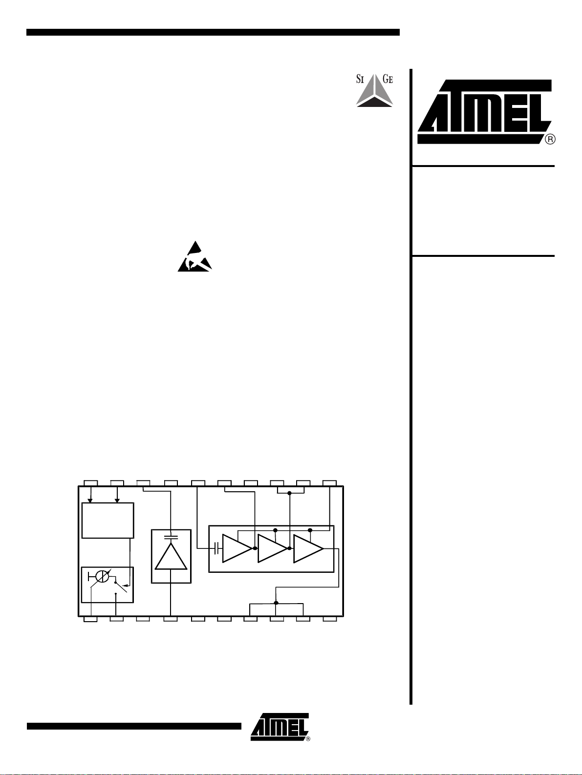
The T7024 is a monolithic SiGe transmit/receive front-end IC with power amplifier,
low-noise amplifier and T/R switch driver. It is especially designed for operation in
TDMA systems like Bluetooth
™
, DECT, and many other IS M app li ca tio ns acc ordi ng to
FCC part 15.
Due to the ramp-control feature and a very low quiescent current, an exter nal switch
transistor for V
is not required.
S
Figure 1. Block Diagram
T
U
N
U
P
TX/RX/
standby
control
TX
O
_
O
_
X
R
D
A
N
N
L
G
LNA
A
N
I
P
_
_
A
1
P
V
A
A
P
D
_
N
2
G
V
PA
P
P
M
_
A
2
R
V
SiGe Front End
T7024
Preliminary
H
C
T
I
W
S
_
R
D
T
N
U
G
O
_
H
C
T
I
W
S
A
N
I
N
_
L
A
_
N
S
L
V
T
D
U
N
O
G
_
A
P
_
3
V
T
T
U
O
_
A
P
_
3
V
D
U
N
O
G
_
A
P
_
3
V
Rev. 4533A–BLURF–09/02
1
Page 2
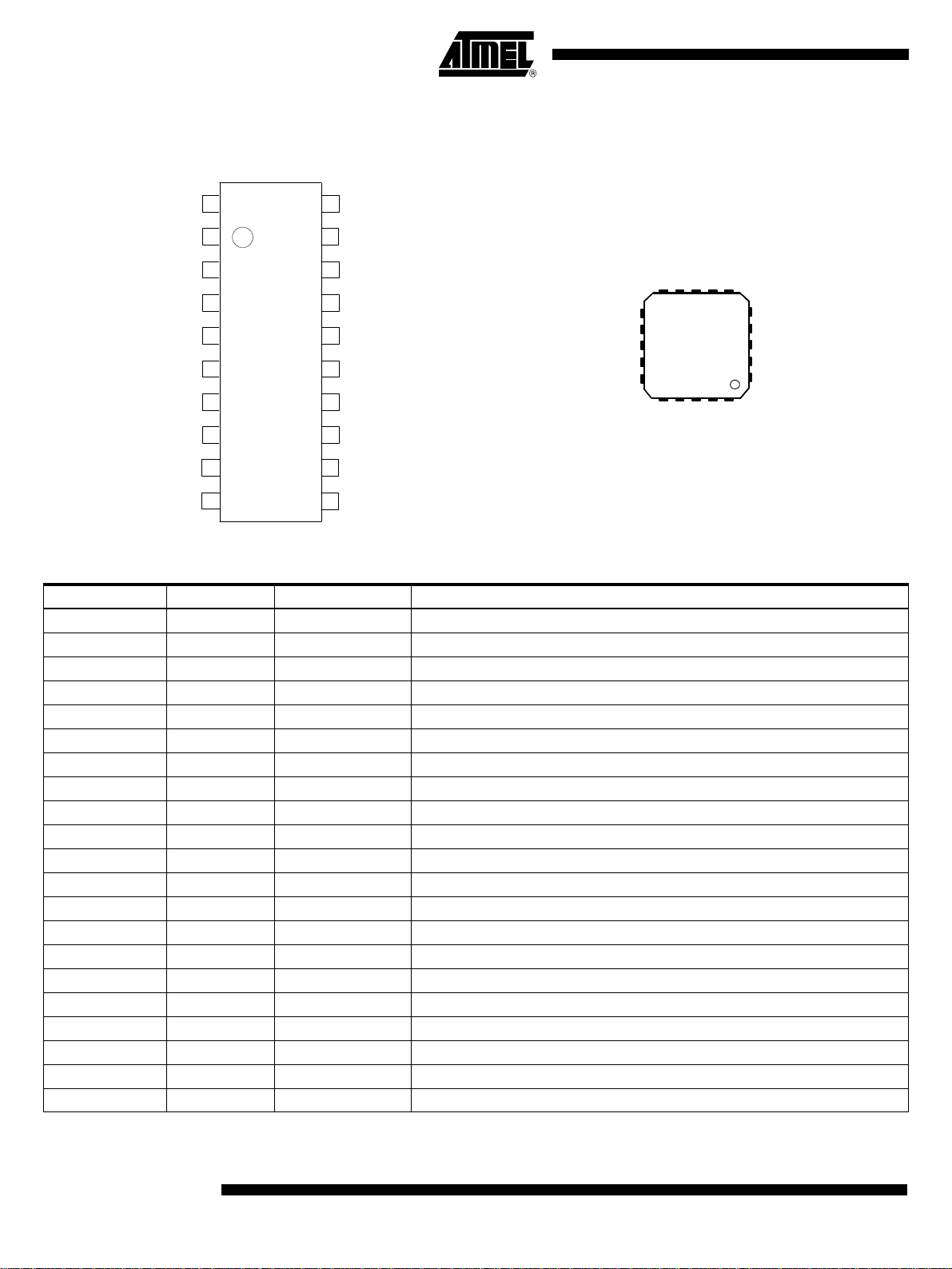
Pin Configuration
Figure 2. Pinning PSSO20 Figure 3. Pinning HP-VFQFP-N20
20
19
18
17
16
15
14
13
12
11
RX_ON
LNA_OUT
GND
PA_IN
V1_PA
GND
V2_PA
V2_PA
RAMP
GND
GND
GND
10
1
2
3
4
5
T7024
6
7
8
9
R_SWITCH PU
SWITCH_OUT
LNA_IN
VS_LNA
V3_PA_OUT
V3_PA_OUT
V3_PA_OUT
Pin Description
Pins PSSO20 Pins N20 Symbol Function
1 4 R_SWITCH Resistor to GND sets the PIN diode current
2 5 SWITCH_OUT Switched current output for PIN diode
36GNDGround
4 7 LNA_IN Low-noise am plifier input
5 9 VS_LNA Supply voltage input for low-noise amplifier
68GNDGround
7 11 V3_PA_OUT Inductor to power supply and matching network for power amplifier output
8 12 V3_PA_OUT Inductor to power supply and matching network for power amplifier output
9 13 V3_PA_OUT Inductor to power supply and matching network for power amplifier output
10 10 GND Ground
11 15 RAMP Power ramping control input
12 16 V2_PA Inductor t o power supply for power amplifie r
13 17 V2_PA Inductor t o power supply for power amplifie r
14 14 GND Ground
15 19 V1_PA Supply voltage for power amplifier
16 20 PA_IN Power amplifier input
17 18 gnd Ground
18 1 LNA_OUT Low-noise amplifier output
19 2 RX_ON RX ac tive high
20 3 PU Power-up active high
Slug Slug GND Ground
V3_PA_OUT
V3_PA_OUT
V3_PA_OUT
GND
RAMP
D
N
G
10 6789
11
12
13
T7024
14
15
16 2019
17
A
P
_
2
V
A
N
I
N
_
L
_
S
V
A
P
_
2
V
D
D
A
N
N
N
G
L
G
5
SWITCH_OUT
4
R_SWITCH
3
PU
2
RX_ON
1
A
P
_
1
V
N
I
_
A
P
LNA_OUT
18
D
N
G
2
T7024
4533A–BLURF–09/02
Page 3
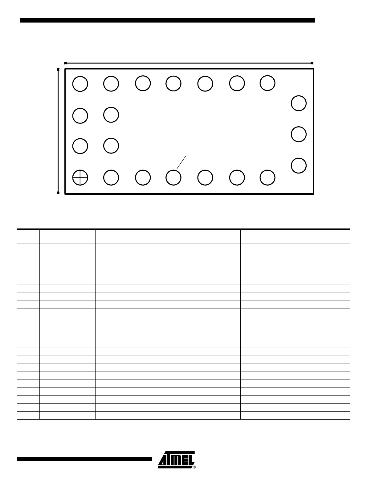
Figure 4. Pad Location, Thickness: 450 µm
T7024
3180 µm
19
LNA_OUT
m
µ
0
0
6
1
20
12
R_SWITCH SWITCH_OUT
3
GND LNA_IN GND
18
21
17
PURX_ON
16
15
14
GNDGNDV1_PAPA_INGND
Pad diameter 180 µm
Ball diameter 200 µm
4
56 7
VS_LNA
GND GND V3_PA_OUT
8
13
V2_PA
9
12
RAMP
11
GND
10
GND
Pad Description
X-Coordinate of
Pad Symbol Function
Pad
(1)
(µm)
1 R_SWITCH Resistor to GND sets the PIN diode current 0 400
2 SWITCH_OUT Switched current output for PIN diode 400 400
3 GND Ground 0 0
4 LNA_IN Low-noise amplifier input 400 0
5 GND Ground 800 0
6 VS_LN A Supply volta ge input for low-noise amplifier 1200 0
7 GND Ground 1600 0
8 GND Ground 2000 0
9 V3_PA_OUT Inductor to power supply and matching network for
2400 0
power amplifier output
10 GND Ground 2780 150
11 GND Ground 2780 550
12 RAMP Power ramping control input 2780 950
13 V2_PA Inductor to power supply for power amplifier 2450 1200
14 GND Ground 2050 1200
15 GND Ground 1650 1200
16 V1_PA Supply voltage for power amplifier 1250 1200
17 PA_IN Power amplifier input 850 1200
18 GND Ground 400 1200
19 LNA_OUT Low-noise amplifier output 0 1200
20 RX_ON RX active high 0 800
21 PU Power-up active high 400 800
Note: 1. Relative to center of Pad 3.
Y-Coordinate of
Pad
(1)
(µm)
4533A–BLURF–09/02
3
Page 4

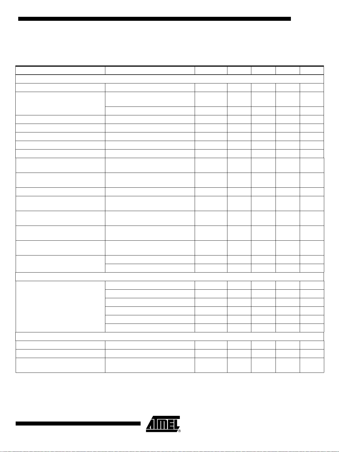
Absolute Maximum Ratings
Parameters Symbol Value Unit
Supply voltage
V
S
6V
Pins VS_LNA, V1_PA, V2_PA, V3_PA_OUT
Junction tem p erature T
Storage temperature T
RF input power LNA P
RF input power PA P
j
stg
inLNA
inPA
150 °C
-40 to +125 °C
5dBm
10 dBm
Thermal Resistance
Parameters Symbol Value Unit
Junction ambient PSSOP20, slug soldered on PCB R
Junction ambient HP-VFQFP-N20, slug soldered on PCB R
thJA
thJA
19 K/W
27 K/W
Operating Range
All voltages are referred to ground (Pins GND and slug). Power supply points are VS_LNA, V1_PA, V2_PA, V3_PA_OUT.
The table represents the sum of all supply currents depending on the TX/RX mode.
Parameters Symbol Min. Typ. Max. Unit
Supply voltage Pins V1_PA, V2_PA and
V3_PA_OUT
Supply voltage Pin VS_LNA V
Supply current TX PSSO20
N20
RX
Standby current PU = 0 I
Ambient temperature T
V
S
S
I
S
I
S
I
S
S_standby
amb
2.7 3.0 4.6 V
2.7 3.0 5.5 V
190
165
8
mA
mA
mA
10 µA
-25 +25 +70 °C
4
T7024
4533A–BLURF–09/02
Page 5
Electrical Characteristics
T7024
Test conditions (unless otherwise specified): VS = 3.0 V, T
Parameters Test Condit ions
Power Amplifier
Supply voltage Pins V1_PA, V2_PA, V3_PA_OUT V
Supply current TX PSSO20
Standby curren t Standby I
(1)
N20
RX (PA off), V
£ 0.1 V I
RAMP
amb
= 25°C
Symbol Min. Typ. Max. Unit
S
I
S_TX
I
S_TX
S_RX
S_standby
2.7 3.0 4.6 V
190
165
mA
mA
10 µA
10 µA
Frequency range TX f 2.4 2.5 GHz
Gain-control ra nge TX
DGp 60 42 dB
Power gain maximum TX, Pin PA_IN to V3_PA_OUT Gp 28 30 33 dB
Power gain minimum TX, Pin PA_IN to V3_PA_OUT Gp -40 -17 dB
Ramping voltage maximum TX, power gain (maximum)
Pin RAMP
Ramping v o ltage minimum TX, power gain (minimum)
Pin RAMP
Ramping current maximum TX, V
= 1.75 V, Pin RAMP I
RAMP
Power-added efficiency TX PSSO20
N20
Saturated output power TX, input power = 0 dBm referred to
Pins V3_PA_OUT
Input matching
Output matching
(2)
(2)
TX, Pin PA_IN Load
TX, Pins V3_PA_OUT Load
V
RAMP max
V
RAMP min
RAMP max
PAE
PAE
P
sat
VSWR
VSWR
1.7 1.75 1.83 V
0.1 V
0.5 mA
30
35
35
40
22.0 23 24.0 dBm
<1.5:1
<1.5:1
Harmonics at P 1dBCP TX, Pins V3_P A_OUT 2 fo -30 dBc
TX, Pins V3_PA_OUT 3 fo -30 dBc
T/R Switch Driver (Current Programming by External Resistor from R_SWITCH to GND)
Switch-out current output Standby, Pin SWITCH_OUT I
RX I
W I
W I
W I
¥ I
Low-noise Amplifier
TX at 100
TX at 1.2 k
TX at 33 k
TX at
(3)
S_O_standby
S_O_RX
S_O_100
S_O_1k2
S_O_33k
S_O_R
Supply voltage All, Pin VS_LNA V
Supply current RX I
Supply current
(LNA and control logic)
TX (control logic active)
Pin VS_LNA
1.7 mA
7mA
17 mA
19 mA
S
S
I
S
2.7 3.0 5.5 V
89mA
1µA
1µA
0.5 mA
Notes: 1. Power amplifier shall be unconditionally stable, maximum duty cycle 100%, true CW operation, maximum load mismatch
and duration: load VSWR = 10:1 (all phases) 10 s, Z
2. With external matching network, load impedance 50
= 50 W.
C
W.
3. Low-noise amplifier shall be unconditionally stable.
4. With external matching components.
%
%
4533A–BLURF–09/02
5
Page 6
Electrical Characteristics (Continued)
Test conditions (unless otherwise specified): VS = 3.0 V, T
Parameters Test Condit ions
Standby curren t Standby, Pin VS_LNA I
amb
= 25°C
Symbol Min. Typ. Max. Unit
S_standby
110µA
Frequency range RX f 2.4 2.5 GHz
Power gain RX, Pin LNA_IN to LNA_OUT Gp 15 16 19 dB
Noise figure RX, PSSO20
N20
Gain compression RX,
referred to PinLNA_OUT
rd
-order input interception point RX IIP3 -16 -14 -13 dBm
3
Input matching
Output matching
(4)
(4)
RX, Pin LNA_IN VSWRin 2:1
RX Pin LNA_OUT VSWRout 2:1
NF
NF
2.5
2.1
2.8
2.3
dB
O1dB -9 -7 -6 dBm
Logic input levels (RX_ON, PU)
High input level = ‘1’ Pins RX_ON and PU V
Low input level = ‘0’ V
High input current = ‘1’ V
= 2.4 V I
iH
Low input current = ‘0’ I
iH
iL
iH
iL
2.4 V
S, LNA
00.5V
40 60 µA
0.2 µA
Notes: 1. Power amplifier shall be unconditionally stable, maximum duty cycle 100%, true CW operation, maximum load mismatch
and duration: load VSWR = 10:1 (all phases) 10 s, Z
2. With external matching network, load impedance 50
= 50 W.
C
W.
3. Low-noise amplifier shall be unconditionally stable.
4. With external matching components.
V
Control Logic for LNA and T/R Switch Driver
Operation Mode PU RX_ON
Standby 0 0
TX 1 0
RX 1 1
6
T7024
4533A–BLURF–09/02
Page 7

Typical Operating Characteristics
Figure 5. LNA (PSSO20): Gain and Noise Figure versus Frequency
T7024
20
15
10
Gain
Gain (dB)
5
0
2000 2200 2400 2600 2800 3000
Frequency (MHz)
Figure 6. LNA (N20): Gain and Noise Figure versus Frequency
25
20
15
10
Gain (dB)
Gain
8
7
6
5
NF
4
NF (dB)
3
2
1
0
5
4
3
NF
2
NF (dB)
5
0
2000 2200 2400 2600 2800 3000
Frequency (MHz)
Figure 7. LNA: NF and Gain vers us Temperature
2.5
2.0
1.5
1.0
0.5
0.0
-0.5
Relative gain,
relative NF (dB)
-1.0
-1.5
-2.0
-2.5
-40-20 02040 6080
NF
Gain
Temperature (°C)
1
0
VS = 3 V
4533A–BLURF–09/02
7
Page 8

Figure 8. LNA: Typical Switch-out Current versus R
20
16
12
(mA)
8
S_O
I
4
0
1 10 100 1000 10000 100000 1000000 10000000
R
(W)
switch
switch
Figure 9. PA (PSSO20): Output Power and PAE versus Supply
50
I_S_TX
40
30
20
Pout (dBm), PAE (%)
PAE
Pout
f = 2.4 GHz
= 1.75 V
V
ramp
P
= 0 dBm
10
0
2.7 3.1 3.5 3.9 4.3 4.7
inPA
250
220
190
160
130
100
Supply Voltage (MHz)
Figure 10. PA (PSSO20): Output Power and PAE versus Ramp Voltage
Pout (dBm), PAE (%)
-30
30
-10
50
PAE
10
I_S_TX
f = 2.4 GHz
V
= 3 V
S
P
= 0 dBm
inPA
Pout
250
200
150
100
50
I_S_TX (mA)
I_S_TX (mA)
-50
1.2 1.4 1.6 1.8 2.0
V
(V)
ramp
8
T7024
0
4533A–BLURF–09/02
Page 9

Figure 11. PA (PSSO20): Output Po wer and PAE versus Input Power
T7024
40
Gain
30
20
10
0
I_S_TX
Pout (dBm), PAE (%), Gp (dB)
-10
Pout
-40 -30 -20 -10 0 10
VS = 3 V
f = 2.4 GHz
V
= 1.75 V
ramp
= 0 dBm
Pi
nPA
PAE
Input Power (dBm)
Figure 12. PA (PSSO20): Output Power and PAE versus Frequency
50
Pout
I_S_TX
V
ramp
P
inPA
VS = 3 V
= 1.7 V
= 0 dBm
Pout (dBm), PAE (%)
40
30
20
10
PAE
250
200
150
100
50
250
200
150
100
50
0
I_S_TX (mA)
0
2400 2420 2440 2460 2480 2500
Frequency (MHz)
Figure 13. PA (N20): Output Power and PAE versus Supply Voltage
50
Pout (dBm), PAE (%)
40
30
20
10
0
PAE
I_S_TX
Pout
f = 2.4 GHz
V
= 1.8 V
ramp
P
= 0 dBm
inPA
2.7 3.1 3.5 3.9 4.3 4.7
Supply Voltage (MHz)
0
250
220
190
160
I_S_TX (mA)
130
100
4533A–BLURF–09/02
9
Page 10

Figure 14. PA (N20) Output Power and PAE versus Ramp Voltage
50
30
10
-10
Pout (dBm), PAE (%)
-30
-50
1.2 1.4 1.6 1.8 2.0
PAE
I_S_TX
Pout
f = 2.4 GHz
= 3 V
V
S
P
= 0 dBm
inPA
V
(V)
ramp
Figure 15. PA (N20): Output Power and PAE versus Input Power
50
40
30
20
10
0
Pout (dBm), PAE (%), Gp (dB)
-10
-40 -30 -20 -10 0 10
Gain
I_S_TX
Pout
VS = 3 V
f = 2.4 GHz
V
= 1.8 V
ramp
P
= 0 dBm
inPA
Input Power (dBm)
PAE
250
200
150
100
50
0
300
250
200
150
100
50
0
I_S_TX (mA)
I_S_TX (mA)
10
T7024
Figure 16. PA (N20): Output Power and PAE versus Frequency
50
40
30
20
Pout (dBm), PAE (%)
10
0
2400 2420 2440 2460 2480 2500
PAE
Pout
I_S_TX
Frequency (MHz)
V
P
inPA
VS = 3 V
= 1.8 V
ramp
= 0 dBm
250
200
150
100
I_S_TX (mA)
50
0
4533A–BLURF–09/02
Page 11

Figure 17. LNA: Supply Current versus Temperature
8.0
7.8
7.6
7.4
7.2
7.0
6.8
6.6
Supply current (V)
6.4
6.2
6.0
-40-20 0 20406080
Temperature (°C)
T7024
Figure 18. PA (PSSO20): Current versus V
200
180
160
140
120
100
80
I ( dBm )
60
40
20
0
0.1 1.0 10.0 100.0 1000.0
Figure 19. PA (PSSO20, N20): P
30
f = 2.4 GHz
= 3 V
V
S
= 0 dBm
P
20
10
in
V
current ( µA )
ramp
versus V
out
5
and Temperature
ramp
-40°C
0°C
80°C
and Temperature
ramp
40°C
4533A–BLURF–09/02
0
Pout ( dBm )
-10
-20
1.0 1.2 1.4 1.6 1.8
80
25
V
( V )
ramp
-15
-40°C
11
Page 12

Input/Output Circuits
Figure 20. Input Circuit PA_IN/V1_PA
V1_PA
PA_IN
GND
Figure 21. Input Circuit RAMP/V1_PA
Figure 22. Input Circuit V2_PA
V1_PA
RAMP
V2_PA
12
GND
T7024
4533A–BLURF–09/02
Page 13

Figure 23. Input/Output Circuit V3_PA_OUT
V3_PA_OUT
GND
Figure 24. Input Circuit SWITCH_OUT/R_SWITCH
V1_PA
T7024
SWITCH_OUT
GND
Figure 25. Input Circuit LNA_IN/VS_LNA
VS_LNA
LNA_IN
R_SWITCH
4533A–BLURF–09/02
GND
13
Page 14

Figure 26. Input Circuit PU/RX_ON
VS_LNA
LNA_IN /
PU
Figure 27. Output Circuit LNA_OUT
VS_LNA
GND
LNA_OUT
14
T7024
4533A–BLURF–09/02
Page 15

Figure 28. Application Board PSSO20
T7024
RX ON
PU
R1 is selected
with DIL-switch
pin-diode replaced
by LED on applicationboard
R1
Var
100p
100p
Switch Out
3.9nH
5.6nH
3.9p
PA IN
3p3 HQ
16
LNA OUT
20 19 18 17 15 14 13 12 11
T7024
1.8p
5
harm.
termination
15nH
10p
1n
0p8
HQ
1p5 HQ
1u
PA OUTV3_PA
56p
1u
VS_LNALNA IN
1234
1n
1n
15p
56p
109876
Blocking capacitors
depending on application
V1_PA
1u10p
V2_PA
1u
PA ramp
Figure 29. Layout for PSSO20
0R
2k7
0R
390R
LNA_SUPPLY
100pF
DIL-Switch
LED
0R
100pF
3.9nH
1.8pF
0R
LNA_OUT
3.9pF
56pF
1uF
0.8pF HQ
LNA_IN
5.6nH
0R
3.3pF HQ
56pF
15nH
1.5pF HQ
15pF
PA_IN
PA_OUT
1nF
10pF
1nF
1nF
1uF
1uF
1uF
P
A
_
S
U
P
P
L
Y
4533A–BLURF–09/02
15
Page 16

Figure 30. Application Board N20
Gerberfiles are available on request.
The application board consists of 4 layers:
1. top layer: RF-signals, 35 µm Cu
2. spacing: 490 µm FR4
3. second layer: GND, 35 µm Cu
4. spacing: 550 µm FR4
5. third layer: GND (optional), 35 µm Cu
6. spacing: 490 µm FR4
7. bottom layer: DC connection, 35 µm Cu
RX ON
100p
PU
100p
R1 is selected
with DIL-switch
pin-diode replaced
by LED on application-
board
Switch Out
LNA OUT
2.2p
R1
Var
PA IN
1p
171819
1
2
3
4
5
610
1.8p
1620
T7024
789
56p
1u
15
14
13
12
11
3p3
18nH
harm.
termination
2p2
0p8
1n10p
1u
PA OUTV3_PAVS_LNALNA IN
1n15p 1u
1n15p
56p
V1_PA
1u
V2_PA
PA ramp
Blocking capacitors
depending on application
16
T7024
4533A–BLURF–09/02
Page 17

Figure 31. Layout for N20
T7024
LED
0R
390R
100pF
100pF
0.8pF HQ
2k7
2.2pF
1.8pF
0R
LNA_OUT
0R
0R
0R
0R
56p
1 mF
LNA_IN
1pF
15pF
3.3pF
56pF
2.2pF
HQ
PA_IN
0R
0R
HQ
18nH HQ
1nF
1nF
15pF
1nF
10pF
PA_OUT
1 mF
1 mF
1 mF
Gerberfiles are available on request.
The application board consists of 4 layers:
1. top layer: RF-signals, 35 µm Cu
2. spacing: 490 µm FR4
3. second layer: GND, 35 µm Cu
4. spacing: 550 µm FR4
5. third layer: GND (optional), 35 µm Cu
6. spacing: 490 µm FR4
7. bottom layer: DC connection, 35 µm Cu
4533A–BLURF–09/02
17
Page 18

Ordering Information
Extended Type Numb er Package Remarks
T7024-TRS PSSO20 Tube
T7024-TRQ PSSO20 Taped and reeled
T7024-PGS HP-VFQFP-N20 Tube
T7024-PGQ HP-VFQFP-N 20 Taped and reeled
T7024-DB Flipchip –
Package Information
18
T7024
4533A–BLURF–09/02
Page 19

T7024
4533A–BLURF–09/02
19
Page 20

Atmel Headquar ters Atm el Operations
Corporate Headquarters
2325 Orchard Parkway
San Jose, CA 95131
TEL 1(408) 441-0311
FAX 1(408) 487-2600
Europe
Atmel Sarl
Route des Arsenaux 41
Case Postale 80
CH-1705 Fribourg
Switzerland
TEL (41) 26-426-5555
FAX (41) 26-426-5500
Asia
Room 1219
Chinachem Gol d en Pla za
77 Mody Road Tsimhatsui
East Kowloon
Hong Kong
TEL (852) 2721-9778
FAX (852) 2722-1369
Japan
9F, Tonetsu Shinkawa Bldg.
1-24-8 Shinka wa
Chuo-ku, Tokyo 104-0033
Japan
TEL (81) 3- 3523- 3551
FAX (81) 3-3523-7581
Memory
2325 Orchard Parkway
San Jose, CA 95131
TEL 1(408) 441-0311
FAX 1(408) 436-4314
Microcontrollers
2325 Orchard Parkway
San Jose, CA 95131
TEL 1(408) 441-0311
FAX 1(408) 436-4314
La Chantrerie
BP 70602
44306 Nantes Cedex 3, France
TEL (33) 2-40-18-18-18
FAX (33) 2- 40-1 8-19- 60
ASIC/ASSP/Smart Cards
Zone Industrielle
13106 Rousset Cedex, France
TEL (33) 4-42-53-60-00
FAX (33) 4- 42-5 3-60- 01
1150 East Cheyenne Mtn. Blvd.
Colorado Springs, CO 80906
TEL 1(719) 576-3300
FAX 1(719) 540-1759
Scottish Enterprise Technology Park
Maxwell Building
East Kilbride G75 0QR, Scotland
TEL (44) 1355-803-000
FAX (44) 1355-242-743
RF/Automotive
Theresienstrasse 2
Postfach 3535
74025 Heil bronn, Germa ny
TEL (49) 71-31-67-0
FAX (49) 71-31-67-2340
1150 East Cheyenne Mtn. Blvd.
Colorado Springs, CO 80906
TEL 1(719) 576-3300
FAX 1(719) 540-1759
Biometrics/Imaging/Hi-Rel MPU/
High Speed Converters/RF Datacom
Avenue de Rochepleine
BP 123
38521 Saint-Egreve Cedex, France
TEL (33) 4-76-58-30-00
FAX (33) 4- 76-5 8-34- 80
e-mail
literature@atmel.com
Web Site
http://www.atmel.com
© Atmel Corporation 2002.
Atmel Corporation makes no warranty for the use of its products, other than those expressly contained in the Company’s standard warranty
which is detailed in Atmel’s Terms and Conditions located on the Company’s web site. The Company assumes no responsibility for any errors
which may appear in this document, reserves the right to change devices or specifications det ailed herein at any time without notice, and does
not make any commitment to update the information contained herein. No licenses to patents or other intellectual property of Atmel are granted
by the Company in connection with the sale of Atmel products, expressly or by implication. Atmel’s products are not authorized for use as critical
components in life support devices or systems.
Atmel® is the registered trademark of Atmel.
The Bluetooth name and the Bluetooth trademarks are owned by Bluetooth SIG, Inc, and are used by Atmel
Corporation under license.
Other terms and product names may be the trademarks of others.
Printed on recycled paper.
4533A–BLURF–09/02
xM
 Loading...