

Page 1

Features
• Compatible with MCS-51
• 4K Bytes of In-System Programmable (ISP) Flash Memory
– Endurance: 1000 Write/Erase Cycles
• 4.0V to 5.5V Operating Range
• Fully Static Operation: 0 Hz to 33 MHz
• Three-level Program Memory Lock
• 128 x 8-bit Internal RAM
• 32 Programmable I/O Lines
• Two 16-bit Timer/Counters
• Six Interrupt Sources
• Full Duplex UART Serial Channel
• Low-power Idle and Power-do wn Mode s
• Interrupt Recovery from Power-do wn Mode
• Watchdog Timer
• Dual Data Pointer
• Power-off Flag
• Fast Programming Time
• Flexible ISP Programming (Byte and Page Mo de)
®
Products
8-bit
Microcontroller
with 4K Bytes
In-System
Programmable
Description
The AT89S51 is a low-power, high-performance CMOS 8-bit microcontroller with 4K
bytes of in-system programmable Flash memory. The device is manufactured using
Atmel’s high-densit y nonvolatile me mory technology and is com pati ble with t he i ndu stry-standard 80C51 instruction set and pinout. The on-chip Flash allows the program
memory to be reprogrammed in-syst em or by a conventional n onvolatile memory programmer. By combining a versatile 8-bit CPU with in-system programmable Flash on a
monolithic chip, the Atmel AT89S51 is a powerful microcontroller which provides a
highly-flexible and cost-effective solution to many embedded control applications.
The AT89S51 provides the following standard features: 4K bytes of Flash, 128 bytes of
RAM, 32 I/O lines, Watchdog timer, two data pointers, two 16-bit timer/counters, a fivevector two-level interrupt architecture, a full duplex serial port, on-chip oscillator, and
clock circuitry. In addition, the AT89S51 is designed with static logic for operation
down to zero frequency and supports two software selectable power saving modes.
The Idle Mode stops the CPU while allowing the RAM, timer/counters, serial port, and
interrupt syste m to continue fu nctioni ng. The Power-down mode saves the RAM contents but freezes the oscillator, disabling all other c hi p fu nctions until the next external
interrupt or hardware reset.
Flash
AT89S51
Rev. 2487A–10/01
1
Page 2
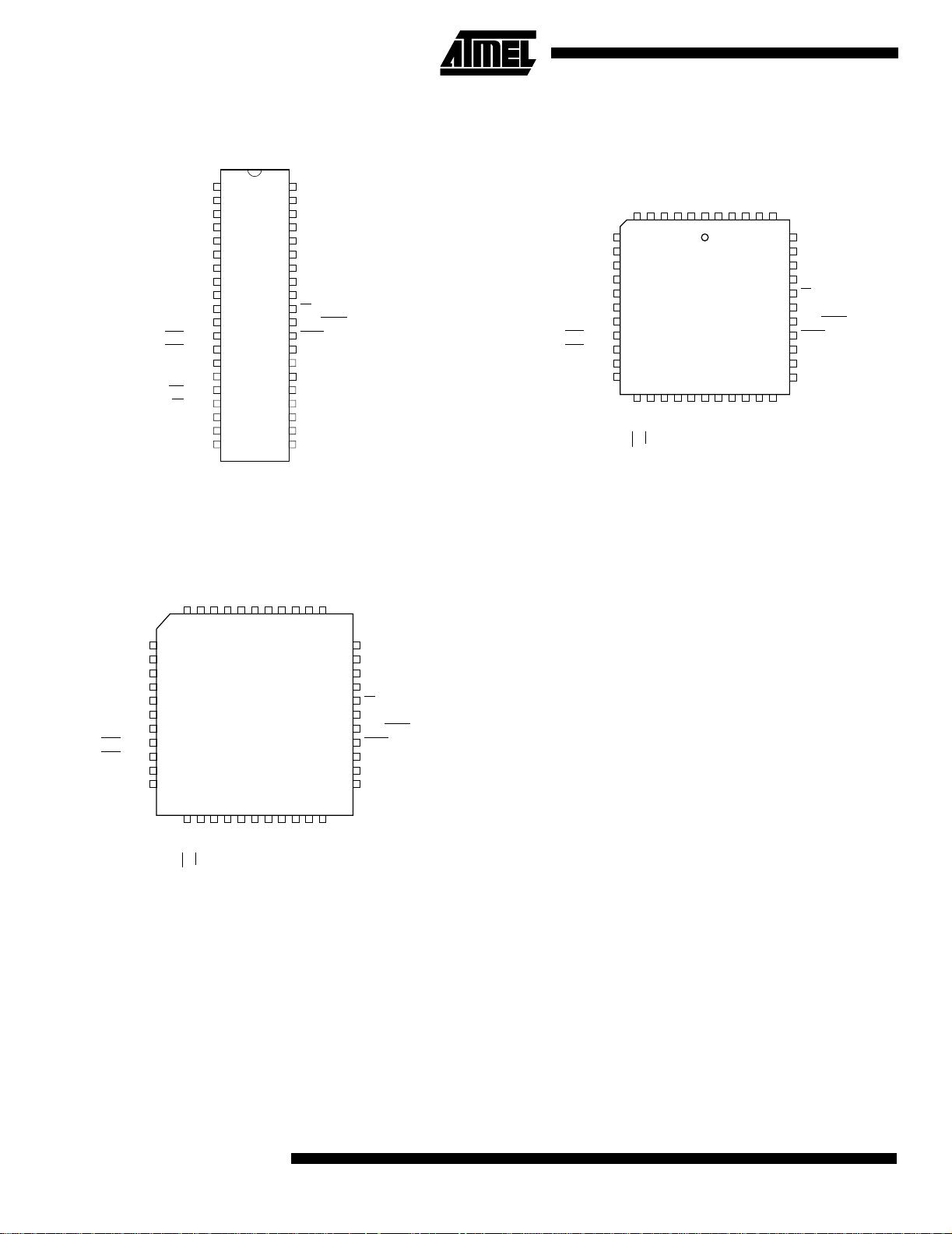
Pin Configurations
PDIP
PLCC
(MOSI) P1.5
(MISO) P1.6
(SCK) P1.7
RST
(RXD) P3.0
NC
(TXD) P3.1
(INT0) P3.2
(INT1) P3.3
(T0) P3.4
(T1) P3.5
1
P1.0
2
P1.1
3
P1.2
4
P1.3
5
P1.4
RST
XTAL2
XTAL1
GND
6
7
8
9
10
11
12
13
14
15
16
17
18
19
20
(MOSI) P1.5
(MISO) P1.6
(SCK) P1.7
(RXD) P3.0
(TXD) P3.1
(INT0) P3.2
(INT1) P3.3
(T0) P3.4
(T1) P3.5
(WR) P3.6
(RD) P3.7
TQFP
P1.4
P1.3
P1.2
P1.1
P1.0 NCVCC
4443424140393837363534
1
2
3
4
5
6
7
8
9
10
11
1213141516171819202122
40
39
38
37
36
35
34
33
32
31
30
29
28
27
26
25
24
23
22
21
P0.0 (AD0)
VCC
P0.0 (AD0)
P0.1 (AD1)
P0.2 (AD2)
P0.3 (AD3)
P0.4 (AD4)
P0.5 (AD5)
P0.6 (AD6)
P0.7 (AD7)
EA/VPP
ALE/PROG
PSEN
P2.7 (A15)
P2.6 (A14)
P2.5 (A13)
P2.4 (A12)
P2.3 (A11)
P2.2 (A10)
P2.1 (A9)
P2.0 (A8)
P0.1 (AD1)
P0.2 (AD2)
P0.3 (AD3)
33
32
31
30
29
28
27
26
25
24
23
P0.4 (AD4)
P0.5 (AD5)
P0.6 (AD6)
P0.7 (AD7)
EA/VPP
NC
ALE/PROG
PSEN
P2.7 (A15)
P2.6 (A14)
P2.5 (A13)
(MOSI) P1.5
(MISO) P1.6
(SCK) P1.7
RST
(RXD) P3.0
NC
(TXD) P3.1
(INT0) P3.2
(INT1) P3.3
(T0) P3.4
(T1) P3.5
P1.4
P1.3
P1.2
P1.1
P1.0 NCVCC
P0.0 (AD0)
65432
7
8
9
10
11
12
13
14
15
16
17
1819202122232425262728
(RD) P3.7
(WR) P3.6
XTAL2
XTAL1
GND
1
NC
4443424140
(A8) P2.0
(A9) P2.1
P0.1 (AD1)
P0.2 (AD2)
P0.3 (AD3)
39
38
37
36
35
34
33
32
31
30
29
(A10) P2.2
(A11) P2.3
(A12) P2.4
P0.4 (AD4)
P0.5 (AD5)
P0.6 (AD6)
P0.7 (AD7)
EA/VPP
NC
ALE/PROG
PSEN
P2.7 (A15)
P2.6 (A14)
P2.5 (A13)
GND
GND
XTAL2
XTAL1
(A8) P2.0
(RD) P3.7
(WR) P3.6
2
AT89S51
(A9) P2.1
(A10) P2.2
(A11) P2.3
(A12) P2.4
2487A–10/01
Page 3
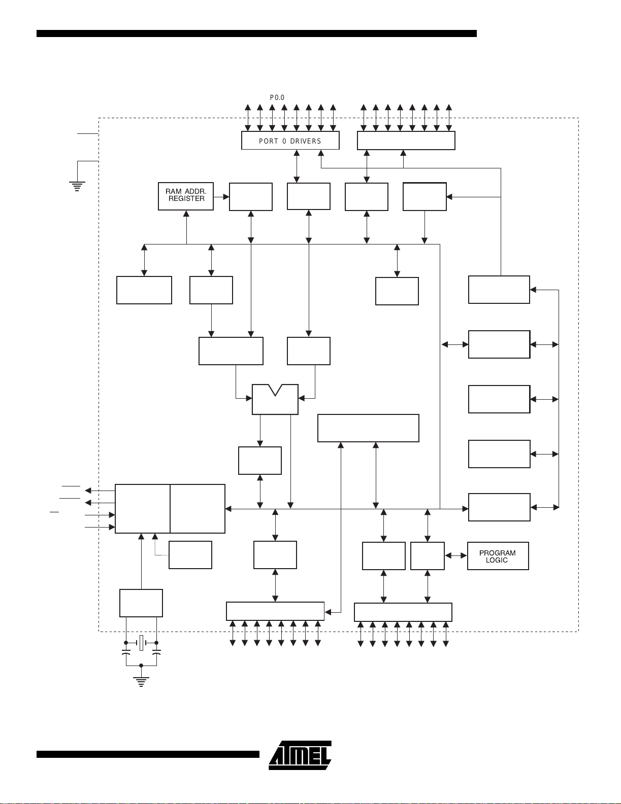
Block Diagram
AT89S51
V
CC
GND
B
REGISTER
RAM ADDR.
REGISTER
P0.0 - P0.7
PORT 0 DRIVERS
RAM
ACC
TMP2 TMP1
PORT 0
LATCH
P2.0 - P2.7
PORT 2 DRIVERS
PORT 2
LATCH
STACK
POINTER
FLASH
PROGRAM
ADDRESS
REGISTER
BUFFER
PSEN
ALE/PROG
EA / V
RST
PC
ALU
INTERRUPT, SERIAL PORT,
AND TIMER BLOCKS
PSW
TIMING
AND
PP
CONTROL
OSC
INSTRUCTION
REGISTER
WATCH
DOG
PORT 3
LATCH
PORT 3 DRIVERS
P3.0 - P3.7
PORT 1
LATCH
PORT 1 DRIVERS
P1.0 - P1.7
ISP
PORT
INCREMENTER
PROGRAM
COUNTER
DUAL DPTR
PROGRAM
LOGIC
2487A–10/01
3
Page 4

Pin Description
VCC Supply voltage. GND Ground. Po rt 0 Port 0 is an 8-bit open drain bidirectional I/O port. As an output port, each pin can sink eight
TTL inputs. When 1s are written to port 0 pins, the pins can be used as high-imped ance
inputs.
Port 0 can also be configured to be the multiplexed low-order address/data bus during
accesses to external program and data memory. In this mode, P0 has internal pull-ups.
Port 0 also recei ves the cod e bytes dur ing Flash pr ogramming and output s the code b ytes
during program verification. External pull-ups are required during program verification.
Po rt 1 Port 1 is an 8-bit bidirectional I/O port with internal pull-ups. The Port 1 output buffers can
sink/source four TTL in puts. When 1s are writte n to Port 1 pins, they a re pulled hig h by the
internal pull-ups and can be u sed as inputs . As inputs, Port 1 p ins that ar e extern ally being
pulled low will source current (I
Port 1 also receives the low-order address bytes during Flash programming and verification.
Port Pin Alternate Functions
) because of the internal pull-ups.
IL
P1.5 MOSI (used for In-System Programming)
P1.6 MISO (used for In-System Programming)
P1.7 SCK (used for In-System Programming)
Po rt 2 Port 2 is an 8-bit bidirectional I/O port with internal pull-ups. The Port 2 output buffers can
sink/source four TTL in puts. When 1s are writte n to Port 2 pins, they a re pulled hig h by the
internal pull-ups and can be u sed as inputs . As inputs, Port 2 p ins that ar e extern ally being
pulled low will source current (I
Port 2 emits the high-order address byte during fetches from external program memory and
during accesses t o e xt er nal d ata mem or y th at u se 1 6- bit ad dr es se s (MO VX @ DP T R). I n t his
application, Port 2 uses strong internal pull-ups when emitting 1s. During accesses to external
data memory that use 8-bit addresses (MOVX @ RI), Port 2 emits the contents of the P2 Special Function Register.
Port 2 also receives th e high-order addr ess bits an d some control signals durin g Flash programming and verification.
) because of the internal pull-ups.
IL
Po rt 3 Port 3 is an 8-bit bidirectional I/O port with internal pull-ups. The Port 3 output buffers can
sink/source four TTL in puts. When 1s are writte n to Port 3 pins, they a re pulled hig h by the
internal pull-ups and can be u sed as inputs . As inputs, Port 3 p ins that ar e extern ally being
pulled low will source current (I
Port 3 receives some control signals for Flash programming and verification.
) because of the pull-ups.
IL
Port 3 also serves the functions of various special features of the AT89S51, as shown in the
following table.
4
AT89S51
2487A–10/01
Page 5

Port Pin Alternate Functions
P3.0 RXD (serial input port)
P3.1 TXD (serial output port)
AT89S51
P3.2 INT0
P3.3 INT1
P3.4 T0 (timer 0 external input)
P3.5 T1 (timer 1 external input)
P3.6 WR
P3.7 RD (external data memory read strobe)
(external interrupt 0)
(external interrupt 1)
(external data memory write strobe)
RST Reset input. A high on this pin for two machine cycles while the oscillator is running resets the
device. This pin drives High for 98 oscillator periods after the Watchdog times out. The DISRTO bit in SFR AUXR (addre ss 8EH) ca n be used to disa ble this feat ure. In the de fault stat e
of bit DISRTO, the RESET HIGH out feature is enabled.
ALE/PROG Address Latch Enable (A LE) is an outpu t pulse for latching the lo w byte of the addr ess durin g
accesses to external memory. This pin is also the program pulse input (PROG
programming.
In normal operation, ALE is e mitted a t a con stant rate of 1/ 6 the oscillator frequenc y and may
be used for external timing or clocking pur poses. Note, however, that one ALE pulse is
skipped during each access to external data memory.
If desired, ALE operation can be disabled by setting bit 0 of SFR location 8EH. With the bit set,
ALE is active only during a MO VX or MOVC ins truction. Otherwise, the pin is weakly pull ed
high. Setting the AL E-disable bit has no effect i f the micro controller is in ex ternal exec ution
mode.
) during Flash
PSEN Program Store Enable (PSEN) is the read strobe to external program memory.
When the AT89S51 is executing code from external program memory, P SEN
twice each machine cycle, except that two PSEN
to external data memory.
activations are ski pped du ring each access
is activated
EA/VPP External Access Enable. EA must be strapped to GND in order to enable the device to fetch
code from external program memory locations starting at 0000H up to FFFFH. Note, however,
that if lock bit 1 is programmed, EA
EA
should be strapped to VCC for internal program executions.
This pin also receives the 12-volt programming enable voltage (V
programming.
will be internally latched on reset.
) during Flash
PP
XTAL1 Input to the inverting oscillator amplifier and input to the internal clock operating circuit. XTAL2 Output from the inverting oscillator amplifier
2487A–10/01
5
Page 6

Special Function Registers
A map of the on-chip memory area called the Special Function Register (SFR) space is shown
in Table 1.
Note that not all of the addresses are occupied, and unoccupied addresses may not be implemented on the chip . Read acces ses to these addre sses will in gene ral retur n random dat a,
and write accesses will have an indeterminate effect.
Table 1. AT89S51 SFR Map and Reset Values
0F8H 0FFH
0F0H
0E8H 0EFH
0E0H
0D8H 0DFH
0D0H
0C8H 0CFH
0C0H 0C7H
0B8H
0B0H
0A8H
0A0H
98H
90H
88H
80H
B
00000000
ACC
00000000
PSW
00000000
IP
XX000000
P3
11111111
IE
0X000000
P2
11111111
SCON
00000000
P1
11111111
TCON
00000000
P0
11111111
SBUF
XXXXXXXX
TMOD
00000000
SP
00000111
AUXR1
XXXXXXX0
TL0
00000000
DP0L
00000000
TL1
00000000
DP0H
00000000
TH0
00000000
DP1L
00000000
TH1
00000000
DP1H
00000000
WDTRST
XXXXXXXX
AUXR
XXX00XX0
PCON
0XXX0000
0F7H
0E7H
0D7H
0BFH
0B7H
0AFH
0A7H
9FH
97H
8FH
87H
6
AT89S51
2487A–10/01
Page 7

AT89S51
User software should not write 1s to these unlisted locations, since they may be used in future
products to invoke new features. In that case, the reset or inactive values of the new bits will
always be 0.
Interrupt Registers: The individual interrupt enable bits are in the IE register. Two priorities
can be set for each of the five interrupt sources in the IP register.
Table 2. AUXR: Auxiliar y Regi ster
AUXR Address = 8EH Reset Value = XXX00XX0B
Not Bit
Addressable
– – – WDIDLE DISRTO – – DISALE
Bit 765 4 3 2 1 0
– Reserved for future expansion
DISALE Disable/Enable ALE
DISALE
Operating Mode
0 ALE is emitted at a constant rate of 1/6 the oscillator frequency
1 ALE is active only during a MOVX or MOVC instruc tion
DISRTO Disable/Enable Reset out
DISRTO
0 Reset pin is driven High after WDT times out
1 Reset pin is input only
WDIDLE Disable/Enable WDT in IDLE mode
WDIDLE
0 WDT continues to count in IDLE mode
1 WDT halts counting in IDLE mode
Dual Data Pointer Registers: To facilitate accessing both internal and external data memory,
two banks of 16-bit Data Pointer Registers are provided: DP0 at SFR address locations 82H83H and DP1 at 84H-85H. Bit DPS = 0 in SFR AUXR1 selects DP0 and DPS = 1 selects DP1.
The user should always initialize the DPS bit to the appropr iate value before accessing the
respective Data Pointer Register .
2487A–10/01
7
Page 8

Power Off Flag: The Power Off Flag (POF) is located at bit 4 (PCON.4) in the PCON SFR.
POF is set to “1” during power up. It can be set and rest under software control and is not
affected by reset.
Table 3. AUXR1: Auxiliary Register 1
AUXR1
Address = A2H
Reset Value = XXXXXXX0B
Not Bit
Addressable
––––– – – DPS
Bit76543 2 1 0
– Reserved for future expansion
DPS Data Pointer Register Select
DPS
0 Selects DPTR Registers DP0L, DP0H
1 Selects DPTR Registers DP1L, DP1H
Memory Organization
MCS-51 devices have a separate address space for Program and Data Memory. Up to 64K
bytes each of external Program and Data Memory can be addressed.
Program Memory If the EA pin is connected to GND, all program fetches are directed to external memory.
On the AT89S51, if EA
FFFH are directed to internal memory and fetches to add resses 1000H through FFFFH are
directed to external memory.
is connected to VCC, program fetches to addresses 0000H through
Data Memory The AT89S51 implemen ts 128 by tes of on- chip RAM. T he 128 byte s are acce ssi ble via direct
and indirect addr essing mo des. Stack oper ations ar e examples of indir ect addres sing, so the
128 bytes of data RAM are available as stack space.
Watchdog Timer (One-time Enabled with Reset-out)
The WDT is intended as a recover y method in s ituations where the CPU may be subjected to
software upsets. The W DT consists of a 14-bit counter an d the Watchdog Ti mer Reset
(WDTRST) SFR. The WDT is defaulted to disable from exiting reset. To enable the WDT, a
user must write 01EH and 0E1H in sequence to the WDTRST register (SFR location 0A6H).
When the WDT is enabled, it will increment every machine cycle while the oscillator is running.
The WDT timeout period is dependent on the external clock frequency. There is no way to disable the WDT except through reset (either hardware reset or WDT overflow reset). When
WDT overflows, it will drive an output RESET HIGH pulse at the RST pin.
Using the WDT To enable the WDT, a user mus t write 01EH and 0E 1H in seq uence to the WDTR ST reg ister
(SFR location 0A6H) . Wh en the WDT is e nabled, the user needs to s ervi ce it by writing 01EH
and 0E1H to WDTRST to avoid a WDT overflow. The 14-bit counter overflows when it reaches
16383 (3FFFH), and this will reset the device. When the WDT is enabled, it will increment
every machin e cyc le w hile th e osc illa tor is r unnin g. T his m ean s the user mu st r ese t the WD T
at least every 1638 3 machin e cycles . To res et the WDT th e user mus t write 01E H and 0E1 H
to WDTRST. WDTRST is a write-only register. The WDT counter canno t be read or written.
When WDT overflows , it will generat e an output RESET pulse at the RST pin . The RESET
pulse duration is 98xTO SC, where TOSC=1/F OSC. To make the best use of the WDT, it
8
AT89S51
2487A–10/01
Page 9

AT89S51
should be serviced in those sections of code that will periodically be executed within the time
required to prevent a WDT reset.
WDT During Power-down and Idle
In Power-down m ode t he os cilla tor st ops, whic h mea ns the WDT also stop s. W hile in Po werdown mode, the user does not need to ser vice the WDT . There are two me thods of exitin g
Power-down mode : by a hardware rese t or via a level -activated ex ternal inte rrupt, which is
enabled prior to entering Power-down mode. When Power-down is exited with hardware reset,
servicing the WDT should occur as it normally does whenever the AT89S51 is reset. Exiting
Power-down with an interrupt is significantly different. The interrupt is held low long enough for
the oscillator to st abilize. When the interrupt is br ought hig h, the interr upt is serv iced. To pr event the WDT from resetting the device while the interrupt pin is held low, the WDT is not
started until the interrupt is pulled high. It is sug ges ted that the W D T be re se t du ring t he i nte rrupt ser vice for the interrupt used to exit Power-down mode.
To ensure that the WDT does not overflow within a few states of exiting Power-down, it is best
to reset the WDT just before entering Power-down mode.
Before going into the IDLE mode, the WDIDLE bit in SFR AUXR is used to determine whether
the WDT continues to cou nt if en abled. The WDT ke eps coun tin g during IDLE (W DIDLE bi t =
0) as the default state . To preve nt the WDT from reset ting the AT8 9S51 whi le in IDLE mode ,
the user should always set up a timer that will periodically exit IDLE , service the WDT , and
reenter IDLE mode.
With WDIDLE bit enabled, the WDT will stop to count in IDLE mode and resumes the count
upon exit from IDLE.
UART The UART in the AT89S 51 operates the sa me way as the UART in the AT89C51. For further
information on the UART operation, refer to the ATMEL Web site (http://www.atmel.com).
From the home page, select ‘Products’, then ‘8051-Architecture F lash Microcontrolle r’, then
‘Product Overview’.
Timer 0 and 1 Timer 0 and Timer 1 in the AT89S51 operate the same way as Timer 0 and Timer 1 in the
AT89C51. For further information on the timers’ operation, refer to the ATMEL Web site
(http://www.atmel.com). From the home page, select ‘Products’, then ‘8051-Architecture Flash
Microcontroller’, then ‘Product Overview’.
Interrupts The AT89S51 has a total of five interrupt vectors: two external interrupts (INT0 and INT1), two
timer interrupts (Timers 0 and 1), and the serial port interrupt. These interrupts are all shown in
Figure 1.
Each of these interrupt sources can be individually enabled or disabled by setting or clearing a
bit in Special Function Register IE. IE also contains a global disable bit, EA, which disables all
interrupts at once.
Note that Table 4 sh ows tha t bit pos ition IE.6 is unimpl emente d. In the A T89S51 , bit pos ition
IE.5 is also unimplemented. User software should not write 1s to these bit positions, since they
may be used in future AT89 products.
The Timer 0 and Timer 1 flags, T F0 and TF1, ar e set at S5 P2 of the cy cle in w hich the time rs
overflow. The values are then polled by the circuitry in the next cycle
2487A–10/01
9
Page 10

.
Table 4. Interrupt Enable (IE) Register
(MSB) (LSB)
EA – – ES ET1 EX1 ET0 EX0
Enable Bit = 1 enables the interrupt.
Enable Bit = 0 disables the interrupt.
Symbol Position Function
EA IE.7 Disables all interrupts. If EA = 0, no interrupt is
acknowledged. If EA = 1, each interrupt source is
individually enabled or disabled by setting or clearing
its enable bit.
– IE.6 Reserved
– IE.5 Reserved
ES IE.4 Serial Port interrupt enable bit
ET1 IE.3 Timer 1 interrupt enable bit
EX1 IE.2 External interrupt 1 enable bit
ET0 IE.1 Timer 0 interrupt enable bit
EX0 IE.0 External interrupt 0 enable bit
User software should never write 1s to reserved bits, because they may be used in future AT89
products.
Figure 1. Interrupt Sources
INT0
TF0
INT1
TF1
RI
0
1
0
1
TI
IE0
IE1
10
AT89S51
2487A–10/01
Page 11

AT89S51
Oscillator Characteristics
XTAL1 and XTAL2 are th e input an d outpu t, respec tively , of an inv erting am plifie r that c an be
configured for use as an on-chi p oscilla tor, as show n in Figure 2. Eith er a quartz c rystal or
ceramic resona tor may be used. To dr ive the d evice fr om an e xternal c lock source, XTAL2
should be left unconnected while XTAL1 is driven, as shown in Figure 3. There are no requirements on the duty cycl e of the external cloc k signal, sinc e the input to the inter nal clocking
circuitry is through a divide-by-two flip-flop, but minimum and maximum voltage high and low
time specifications must be observed.
Figure 2. Oscillator Connections
C2
C1
Note: C1, C2 = 30 pF ± 10 pF for Crystals = 40 pF ± 10 pF for Ceramic Resonators
XTAL2
XTAL1
GND
Figure 3. External Clock Drive Configuration
NC
EXTERNAL
OSCILLATOR
SIGNAL
XTAL2
XTAL1
GND
Idle Mode In idle mode, the CP U puts its elf to slee p while all th e on-ch ip periphe rals rem ain activ e. The
mode is invok ed by software. The content of the on-chip RAM a nd all the sp ecial func tion
registers remain unchanged during this mode. The idle mode can be terminated by any
enabled interrupt or by a hardware reset.
Note that when idle mode is terminated by a hardware reset, the device normally resumes program execution from where it left off, up to two machine cycles before the internal reset
algorithm takes cont rol. On-ch ip hardware i nhibits acce ss to inte rnal RAM in this even t, but
access to the port pins is not inhibited. To el im ina te th e possibility of an unex pec te d wr ite to a
port pin when idle mode is terminated by a reset, the instruction following the one that invokes
idle mode should not write to a port pin or to external memory.
Power-down Mode
In the Power-down mode, the oscillator is stopped, and the instruction that invokes Powerdown is the last in st ructi on e xe cu ted. Th e on -c hip RA M a nd S pec ia l F un cti on Registers retain
their values until the Power-down mode is terminated. Exit from Power-down mode can be initiated either by a hardware rese t or by activation of an ena bled externa l interrupt in to INT0
. Reset redefi nes the SF Rs but does not cha nge the o n-chip RAM . The reset sho uld not
INT1
be activated be fore V
is restored to its norm al op erat ing l evel a nd mu st b e h eld active long
CC
or
enough to allow the oscillator to restart and stabilize.
2487A–10/01
11
Page 12

Table 5. Status of External Pins During Idle and Power-down Modes
Mode Program Memory ALE PSEN PORT0 PORT1 PORT2 PORT3
Idle Internal 1 1 Data Data Data Data
Idle External 1 1 Float Data Address Data
Power-down Internal 0 0 Data Data Data Data
Power-down External 0 0 Float Data Data Data
Program Memory Lock Bits
Programming the Flash – Parallel Mode
The AT89S51 has three lock bits that can be left unprogrammed (U) or can be programmed
(P) to obtain the additional features listed in the following table.
Table 6. Lock Bit Protection Modes
Program Lock Bits
LB1 LB2 LB3 Protection Type
1 U U U No program lock features
2 P U U MOVC instructions executed from external program
memory are disabled from fetchi ng cod e bytes from int ernal
memory, EA is sampled and latched on reset, and further
programming of the Flash memory is disabled
3 P P U Same as mode 2, but verify is also disabled
4 P P P Same as mode 3, but external execution is also disabled
When lock bit 1 is programmed, the logic level at the EA
reset. If the device is powered up without a reset, the latch initializes to a random value and
holds that value until reset is activated. The latched value of EA
logic level at that pin in order for the device to function properly.
The AT89S51 is shipp ed with the on-chip Flas h memory ar ray ready to be program med. The
programming interface needs a high-voltage (12-volt) program enable signal and is compatible with conventional third-party Flash or EPROM programmers.
The AT89S51 code memory array is programmed byte-by-byte.
pin is sampled and latched durin g
must agree with the current
12
Programming Algorithm: Before programming the AT89S 51, the addre ss, data, and contr ol
signals should be set up acco rding to the Flash pr ogram ming mode ta ble and Figures 13 and
14. To program the AT89S51, take the following steps:
1. Input the desired memory location on the address lines.
2. Input the appropriate data byte on the data lines.
3. Activate the correct combination of control signals.
4. Raise EA
5. Pulse ALE/PROG once to program a byte in the Flash array or the lock bits. The byte-
Data
During a write cycle, an attempted rea d of the la st by te writte n wil l re su lt in the com plement of
the written data on P0.7. Once the write cycle has been completed, true data is valid on all outputs, and the next cycle may begin. Data
been initiated.
AT89S51
/VPP to 12V.
write cycle is self-timed and typically takes no more than 50 µs. Repeat steps 1
through 5, changing the address and data for the entire array or until the end of the
object file is reached.
Polling: The AT89S51 features Data Polling to indi cate the end of a byte write cyc le.
Polling may begin any time after a write cycle has
2487A–10/01
Page 13

AT89S51
Ready/Busy: The progress of byte programming can also be monitored by the RDY/BSY out-
put signal. P3.0 is pulled low after ALE goes high during programming to indicate BUSY
is pulled high again when programming is done to indicate READY.
Program Verify: If loc k bits LB1 and LB2 h av e n ot bee n pr ogrammed, the programme d c od e
data can be read back via the address and data lines for verification. The status of the individual lock bits can be verified directly by reading them back.
Reading the Signature Byte s: The signature bytes are read by the same procedure as a normal verification of locations 000H, 100H, and 200H, except that P3.6 and P3.7 must be pulled
to a logic low. The values returned are as follows.
(000H) = 1EH indicates manufactured by Atmel
(100H) = 51H indicates 89S51
(200H) = 06H
Chip Erase: In the parallel programming mode, a chip erase operation is initiated by using the
proper combination of control signals and by pulsing ALE/PROG
500 ns.
In the serial programm ing mode , a chip era se operati on is init iated by iss uing the Ch ip Erase
instruction. In this mode, chip erase is self-timed and takes about 500 ms.
During chip erase, a serial read from any address location will return 00H at the data output.
low for a duration of 200 ns -
. P3.0
Programming the Flash – Serial Mode
Serial Programming Algorithm
The Code memory array can be programmed using the serial ISP interface while RST is
pulled to V
RST is set high, the Programming Enable instruction needs to be executed first before other
operations can be execute d. Before a repro gramming sequence can occur, a Chip Erase
operation is required.
The Chip Erase operation turns the content of every memory location in the Code array into
FFH.
Either an external system cloc k can be suppl ied at pin XT AL1 or a crystal needs to be c onnected across pins X TAL1 and XT A L2. The max im um se ria l cl oc k (SC K) fre que nc y should be
less than 1/16 of the crystal frequency. With a 33 MHz oscillator clock, the maximum SCK frequency is 2 MHz.
To program and verify th e AT89S51 in the serial pr ogrammin g mode, the fol lowing seq uence
is recommended:
1. Power-up sequence:
Apply power between VCC and GND pins.
Set RST pin to “H”.
If a crystal is not connected across pins XTAL1 and XTAL2, apply a 3 MHz to 33 MHz
clock to XTAL1 pin and wait for at least 10 milliseconds.
2. Enable serial programming by sending the Programming Enable serial instruction to
pin MOSI/P1.5. The frequency of the shift clock supplied at pin SCK/P1.7 needs to be
less than the CPU clock at XTAL1 divided by 16.
3. The Code array is programmed one byte at a time in either the Byte or Page mode.
The write cycle is self-timed and typically takes less than 0.5 ms at 5V.
4. Any memory location can be verified by using the Read instruction that returns the content at the selected address at serial output MISO/P1.6.
5. At the end of a programming session, RST can be set low to commence normal device
operation.
. The serial interface consists of pins SCK, MOSI (input) and MISO (output). After
CC
2487A–10/01
13
Page 14

Power-off sequence (if needed):
Set XTAL1 to “L” (if a crystal is not used).
Set RST to “L”.
Turn V
Data
Polling: The Data Polling feature is also available in the seri al mode. In this mode, du r-
power off.
CC
ing a write cyc le an attempted read of th e l as t byt e w ritten will result in the complement of the
MSB of the serial output byte on MISO.
Serial
Programming
The Instruction Set for Serial Programming follows a 4-byte protocol and is shown in Table 8
on page 18.
Instruction Set
Programming
Interface –
Every code byte in t he Flas h array can be progr ammed by usi ng the a pprop riate c ombina tion
of control si gnals . The wri te op erat ion cycle is self -time d and on ce in it iated , wil l au tomati cally
time itself to completion.
Parallel Mode
All major programming vendors offer worldwide support for the Atmel microcontroller series.
Please contact your local programming vendor for the appropriate software revision.
Table 7. Flash Programming Mod es
ALE/
Mode V
Write Code Data 5V H L
Read Code Data 5V H L H H L L L H H D
Write Lock Bit 1 5V H L
Write Lock Bit 2 5V H L
Write Lock Bit 3 5V H L
CC
RST PSEN
PROG
EA/
V
(2)
12VLHHHH DINA11-8 A 7-0
(3)
12VHHHHH X X X
(3)
12V H H H L L X X X
(3)
12V H L H H L X X X
P2.6 P2.7 P3.3 P3.6 P3.7
PP
P0.7-0
Data
OUT
P2.3-0 P1.7-0
Address
A11-8 A 7-0
Read Lock Bits
1, 2, 3
Chip Erase 5V H L
Read Atmel ID 5V H L H H LLLLL1EH0000 00H
Read Device ID 5V H L H H LLLLL 51H0001 00H
Read Device ID 5V H L H H LLLLL 06H0010 00H
5V H L H H H H L H L
(1)
12VHLHLL X X X
P0.2,
P0.3,
P0.4
XX
Notes: 1. Each PROG pulse is 200 ns - 500 ns for Chip Erase.
2. Each PROG
3. Each PROG
4. RDY/BSY
pulse is 200 ns - 500 ns for Write Code Data.
pulse is 200 ns - 500 ns for Write Lock Bits.
signal is output on P3.0 during programming.
5. X = don’t care.
14
AT89S51
2487A–10/01
Page 15

Figure 4. Programming the Flash Memory (Parallel Mode)
AT89S51
P1.0-P1.7
P2.0 - P2.3
P2.6
P2.7
P3.3
P3.6
P3.7
XTAL2 EA
V
P0
ALE
CC
ADDR.
0000H/FFFH
SEE FLASH
PROGRAMMING
MODES TABLE
A0 - A7
A8- A11
AT89S51
V
CC
PGM
DATA
PROG
V/V
IH PP
3-33 MHz
1
XTAL
GND
Figure 5. Verifying the Flash Memory (Parallel Mode)
AT89S51
ADDR.
0000H/FFFH
SEE FLASH
PROGRAMMING
MODES TABLE
3-33 MHz
A0 - A7
A8- A11
P1.0-P1.7
P2.0 - P2.3
P2.6
P2.7
P3.3
P3.6
P3.7
XTAL2 EA
XTAL1
GND
P3.0
RST
PSEN
ALE
RST
PSEN
RDY/
BSY
V
IH
V
CC
V
CC
PGM DATA
P0
(USE 10K
PULLUPS)
V
IH
V
IH
2487A–10/01
15
Page 16

Flash Programming and Verification Characteristics (Parallel Mode)
TA = 20°C to 30°C, VCC = 4.5 to 5.5V
Symbol Parameter Min Max Units
V
PP
I
PP
I
CC
1/t
t
AVGL
t
GHAX
t
DVGL
t
GHDX
t
EHSH
t
SHGL
t
GHSL
t
GLGH
t
AVQV
t
ELQV
t
EHQZ
t
GHBL
t
WC
CLCL
Programming Supply Voltage 11.5 12.5 V
Programming Supp ly Curre nt 10 mA
VCC Supply Current 30 mA
Oscillator Frequency 3 33 MHz
Address Setup to PROG Low 48t
Address Hold After PROG 48t
Data Setup to PROG Low 48t
Data Hold After PROG 48t
P2.7 (ENABLE) High to V
PP
48t
CLCL
CLCL
CLCL
CLCL
CLCL
VPP Setup to PROG Low 10 µs
VPP Hold After PROG 10 µs
PROG Width 0.2 1 µs
Address to Data V al id 48t
ENABLE Low to Data Valid 48t
Data Float After ENABLE 048t
CLCL
CLCL
CLCL
PROG High to BUSY Low 1.0 µs
Byte Write Cycle Time 50 µs
Figure 6. Flash Programming and Verification Waveforms – Parallel Mode
P1.0 - P1.7
P2.0 - P2.3
PORT 0
ALE/PROG
EA/V
PP
P2.7
(ENABLE)
P3.0
(RDY/BSY)
t
AVGL
t
SHGL
PROGRAMMING
ADDRESS
DATA IN
V
t
EHSH
t
PP
DVGL
t
GLGH
t
GHBL
t
GHDX
t
t
ELQV
GHAX
t
GHSL
LOGIC 1
LOGIC 0
BUSY
t
WC
VERIFICATION
ADDRESS
t
AVQV
DATA OUT
READY
t
EHQZ
16
AT89S51
2487A–10/01
Page 17

Figure 7. Flash Memory Serial Downloading
AT89S51
AT89S51
V
CC
V
CC
INSTRUCTION
INPUT
DATA OUTPUT
CLOCK IN
3-33 MHz
P1.5/MOSI
P1.6/MISO
P1.7/SCK
XTAL2
GND
RSTXTAL1
V
IH
Flash Programming and Verification Waveforms – Serial Mode
Figure 8. Serial Programming Waveforms
2487A–10/01
76543210
17
Page 18

Table 8. Serial Programming Instruction Set
Instruction
Format
Instruction
Programming Enable 1010 1100 0101 0011 xxxx xxxx xxxx xxxx
0110 1001
OperationByte 1 Byte 2 Byte 3 Byte 4
Enable Serial Programming
while RST is high
(Output)
Chip Erase 10 10 1100 100x xxxx xxxx xxxx xxxx xxxx Chip Erase Flash memory
array
Read Program Memory
(Byte Mode)
Write Program Me mory
(Byte Mode)
Write Lock Bits
(2)
0010 0000 xxxx Read data from Program
0100 0000 xxxx Write data to Program
1010 1100 1110 00 xxxx xxxx xxxx xxxx Write Lock bits. See Note (2).
A11
A11
A10
A10
B1
A9
A9
A8
B2
A8
A7
A6
A7
A5
A6
A4
A5
A4
A3
A2
A3
A1
A2
A0
A1
A0
D7
D7
D6
D6
D5
D5
D4
D4
D3
D1
D2
D3D2D1
D0
memory in the byte mode
D0
memory in the byte mode
Read Lock Bits 0010 0100 xxxx xxxx xxxx xxxx xx xx Read back current status of
LB1
LB2
LB3
the lock bits (a programmed
lock bit reads back as a “1”)
Read Signature Bytes
Read Program Memory
(Page Mode)
(1)
0010 1000 xxx xxx xxxx Signature Byte Read Signature Byte
0011 0000 xxxx Byte 0 Byte 1...
A5
A4A3A2
A9
A11
A10
A1
A8
A0
Byte 255
Read data from Program
memory in the Page Mode
(256 bytes)
Write Program Me mory
(Page Mode)
0101 0000 xxxx Byte 0 Byte 1...
A9
A8
A11
A10
Byte 255
Write data to Program
memory in the Page Mode
(256 bytes)
Notes: 1. The signature bytes are not readable in Lock Bit Modes 3 and 4.
2. B1 = 0, B2 = 0
B1 = 0, B2 = 1
B1 = 1, B2 = 0
B1 = 1, B1 = 1
→ Mode 1, no lock protection
→ Mode 2, lock bit 1 activated
→ Mode 3, lock bit 2 activated
→ Mode 4, lock bit 3 activated
}
Each of the lock bits needs to be activated sequentially before
Mode 4 can be executed.
18
After Reset signal is high, SCK should be low for at least 64 system clocks before it goes high to clock in the enable data
bytes. No pulsing of Reset signal is necessary. SCK should be no faster than 1/16 of the system clock at XTAL1.
For Page Read/Write, the data always starts from byte 0 to 255. After the command byte and upper ad dress byte are
latched, each byte thereafter is treated as data until all 256 bytes are shifted in/out. Then the next instruction will be ready to
be decoded.
AT89S51
2487A–10/01
Page 19

Serial Programming Characteristics
Figure 9. Serial Programming Timing
MOSI
t
OVSH
t
SHOX
t
SLSH
AT89S51
SCK
t
SHSL
MISO
t
SLIV
Table 9. Serial Progr amming Characteristics, TA = -40°C to 85°C, VCC = 4.0 - 5.5V (Unless Otherwise Noted)
Symbol Parameter Min Typ Max Units
1/t
CLCL
t
CLCL
t
SHSL
t
SLSH
t
OVSH
t
SHOX
t
SLIV
t
ERASE
t
SWC
Oscillator Frequency 0 33 MHz
Oscillator Period 30 ns
SCK Pulse Width High 8 t
SCK Pulse Width Low 8 t
MOSI Setup to SCK High t
MOSI Hold after SCK High 2 t
SCK Low to MISO Valid 10 16 32 ns
Chip Erase Instruction Cycle Time 500 ms
Serial Byte Write Cycle Time 64 t
CLCL
CLCL
CLCL
CLCL
+ 400 µs
CLCL
ns
ns
ns
ns
2487A–10/01
19
Page 20

Absolute Maximum Ratings*
Operating Temperature.................................. -55°C to +125°C
Storage Temperature..................................... -65°C to +150°C
Voltage on Any Pin
with Respect to Ground.....................................-1.0V to +7.0V
Maximum Operating Voltage ............................. ..... ...... ....6.6V
DC Output Current......................................................15.0 mA
*NOTICE: Stresses beyond those listed under “Absolute
Maximum Ratings” may cause permanent damage to the de vice. This is a stress ra ting only and
functional opera tion of the d ev ice at the se or an y
other conditions beyond those indicated in the
operational sections of this specification is not
implied. Exposure to absolute maximum rating
conditions for extended periods may affect
device reliability.
DC Characteristics
The values shown in this table are valid for TA = -40°C to 85°C and VCC = 4.0V to 5.5V, unless otherwise noted.
Symbol Parameter Condition Min Max Units
V
IL
V
IL1
V
IH
V
IH1
V
OL
V
OL1
V
OH
V
OH1
I
IL
I
TL
I
LI
RRST Reset Pulldown Resistor 50 300 KΩ
C
IO
I
CC
Notes: 1. Under steady state (non-transient) conditions, IOL must be externally limited as follows:
2. Minimum VCC for Power-down is 2V.
Input Low Voltage (Except EA)-0.50.2 V
Input Low Voltage (EA)-0.50.2 V
-0.1 V
CC
-0.3 V
CC
Input High Voltage (Except XTAL1, RST) 0.2 VCC+0.9 VCC+0.5 V
Input High Voltage (XTAL1, RST) 0.7 V
Output Low Voltage
1,2,3) I
Output Low Voltage
(Port 0, ALE, PSEN)I
(1)
(Ports
(1)
= 1.6 mA
OL
= 3.2 mA
OL
CC
VCC+0.5 V
0.45 V
0.45 V
IOH = -60 µA, VCC = 5V ± 10% 2.4 V
= -25 µA 0.75 V
I
Output High Voltage
(Ports 1,2,3, ALE, PSEN
)
Output High Voltage
(Port 0 in External Bus Mode)
OH
I
= -10 µA 0.9 V
OH
= -800 µA, VCC = 5V ± 10% 2.4 V
I
OH
= -300 µA 0.75 V
I
OH
I
= -80 µA 0.9 V
OH
Logical 0 Input Current (Ports
1,2,3) V
= 0.45V
IN
Logical 1 to 0 Transition Current
(Ports 1,2,3) V
= 2V, VCC = 5V ± 10%
IN
Input Leakage Current (Port 0,
)0.45 < V
EA
IN
< V
CC
CC
CC
CC
CC
-50 µA
-650 µA
±10 µA
Pin Capacitance Test Freq. = 1 MHz, TA = 25°C 10 pF
Active Mode, 12 MHz 25 mA
Power Supply Current
Power-down Mode
Maximum I
Maximum I
per port pin: 10 mA
OL
per 8-bit port:
OL
(2)
Idle Mode, 12 MHz 6.5 mA
VCC = 5.5V 50 µA
Port 0: 26 mA Ports 1, 2, 3: 15 mA
Maximum total I
exceeds the test condition, V
If I
OL
for all output pins: 71 mA
OL
OL
may exceed the related specification. Pins are not guaranteed to sink current greater
than the listed test conditions.
V
V
V
V
20
AT89S51
2487A–10/01
Page 21

AT89S51
AC Characteristics
Under operating conditions, load capacitance for Port 0, ALE/PROG, and PSEN = 100 pF; load capacitance for all other
outputs = 80 pF.
External Program and Data Memory Characteristics
12 MHz Oscillator Variable Oscillator
Symbol Parameter
1/t
t
LHLL
t
AVLL
t
LLAX
t
LLIV
t
LLPL
t
PLPH
t
PLIV
t
PXIX
t
PXIZ
t
PXAV
t
AVIV
t
PLAZ
t
RLRH
t
WLWH
t
RLDV
t
RHDX
t
RHDZ
t
LLDV
t
AVDV
t
LLWL
t
AVWL
t
QVWX
t
QVWH
t
WHQX
t
RLAZ
t
WHLH
CLCL
Oscillator Frequency 0 33 MHz
ALE Pulse Width 127 2t
Address Valid to ALE Low 43 t
Address Hold After ALE Low 48 t
ALE Low to Valid Instruction In 233 4t
ALE Low to PSEN Low 43 t
PSEN Pulse Width 205 3t
PSEN Low to Valid Instruction In 145 3t
Input Instruction Hold After PSEN 00ns
Input Instruction Float After PSEN 59 t
PSEN to Address Valid 75 t
Address to Valid Instruction In 312 5t
PSEN Low to Address Float 10 10 ns
RD Pulse Width 400 6t
WR Pulse Width 400 6t
RD Low to Valid Data In 252 5t
Data Hold After RD 00ns
Data Float After RD 97 2t
ALE Low to Va lid Data In 517 8t
Address to Valid Data In 585 9t
ALE Low to RD or WR Low 200 300 3t
Address to RD or WR Low 203 4t
Data Valid to WR Transition 23 t
Data Valid to WR High 433 7t
Data Hold After WR 33 t
RD Low to Address Float 0 0 ns
RD or WR High to ALE High 43 123 t
-40 ns
CLCL
-25 ns
CLCL
-25 ns
CLCL
-65 ns
CLCL
-25 ns
CLCL
-45 ns
CLCL
-60 ns
CLCL
-25 ns
CLCL
-8 ns
CLCL
-80 ns
CLCL
-100 ns
CLCL
-100 ns
CLCL
-90 ns
CLCL
-28 ns
CLCL
-150 ns
CLCL
-165 ns
CLCL
-50 3t
CLCL
-75 ns
CLCL
-30 ns
CLCL
-130 ns
CLCL
-25 ns
CLCL
-25 t
CLCL
+50 ns
CLCL
+25 ns
CLCL
UnitsMin Max Min Max
2487A–10/01
21
Page 22

External Pro gr a m Memory Read Cycle
t
LHLL
ALE
t
AVLL
t
LLPL
PSEN
t
LLAX
PORT 0
A0 - A7 A0 - A7
t
AVIV
PORT 2
External Data Memory Read Cycle
t
LHLL
ALE
t
PLAZ
A8 - A15
t
LLIV
t
PLIV
t
PXIZ
t
PXIX
INSTR IN
t
PLPH
t
PXAV
t
A8 - A15
WHLH
PSEN
RD
PORT 0
PORT 2
t
LLDV
t
LLWL
t
LLAX
t
AVLL
A0 - A7 FROM RI OR DPL
t
AVWL
P2.0 - P2.7 OR A8 - A15 FROM DPH
t
AVDV
t
RLAZ
t
RLRH
t
RLDV
DATA IN INSTR IN
t
RHDZ
t
RHDX
A0 - A7 FROM PCL
A8 - A15 FROM PCH
22
AT89S51
2487A–10/01
Page 23

External Data Memory Write Cycle
t
LHLL
ALE
PSEN
t
LLWL
t
WLWH
t
WHLH
AT89S51
WR
t
AVLL
PORT 0
PORT 2
A0 - A7 FROM RI OR DPL
t
AVWL
P2.0 - P2.7 OR A8 - A15 FROM DPH
External Clock Drive Waveforms
t
0.7 V
CC
CHCX
CC
0.45V
V - 0.5V
CC
0.2 V - 0.1V
External Clock Drive
t
LLAX
t
QVWX
t
t
QVWH
DATA OUT INSTR IN
t
CLCH
t
CLCX
WHQX
A0 - A7 FROM PCL
A8 - A15 FROM PCH
t
CHCX
t
CLCL
t
CHCL
Symbol Parameter Min Max Units
1/t
CLCL
t
CLCL
t
CHCX
t
CLCX
t
CLCH
t
CHCL
2487A–10/01
Oscillator Frequency 0 33 MHz
Clock Period 30 ns
High Time 12 ns
Low Time 12 ns
Rise Time 5 ns
Fall Time 5 ns
23
Page 24

Serial Port Timing: Shift Register Mode Test Conditions
The values in this table are valid for V
= 4.0V to 5.5V and Load Capacitance = 80 pF.
CC
Symbol Parameter
t
XLXL
t
QVXH
t
XHQX
t
XHDX
t
XHDV
Serial Port Clock Cycle Tim e 1.0 12t
Output Data Setup to Clock Rising Edge 700 10t
Output Data Hold After Clock Rising Edge 50 2t
Input Data Hold After Clock Rising Edge 0 0 ns
Clock Rising Edge to Input Data Valid 700 10t
Shift Register Mode Timing Waveforms
INSTRUCTION
ALE
CLOCK
WRITE TOSBUF
OUTPUT DATA
CLEAR RI
INPUT DATA
0
t
QVXH
1
t
XHDV
2
t
XLXL
t
XHQX
0
VALID VALIDVALID VALIDVALID VALIDVALID VALID
1
12 MHz Osc Variable Oscillator
CLCL
-133 ns
CLCL
-80 ns
CLCL
3
t
2
XHDX
4
5
3
6
4
7
5
UnitsMin Max Min Max
µs
-133 ns
CLCL
8
6
7
SET TI
SET RI
AC Testing Input/Output Wa veforms
V - 0.5V
CC
0.45V
(1)
0.2 V + 0.9V
0.2 V - 0.1V
CC
TEST POINTS
CC
Note: 1. AC In puts du ring tes tin g are driven at VCC - 0.5V for a logic 1 a nd 0 .45 V for a logic 0. Timing me as urem en ts a r e made at V
min. for a logic 1 and VIL max. for a logic 0.
Float Waveforms
(1)
V
LOAD
V
V
LOAD
LOAD
+ 0.1V
- 0.1V
Timing Reference
Points
- 0.1V
V
OL
+ 0.1V
V
OL
Note: 1. For timing purposes, a port pin is no longer floating when a 100 mV change from load voltage occurs. A port pin begins to
float when a 100 mV change from the loaded V
OH/VOL
level occurs.
IH
24
AT89S51
2487A–10/01
Page 25

Orderi ng Informat ion
Speed
(MHz)
24 4.0V to 5.5V AT89S51-24AC
33 4.5V to 5.5V AT89S51-33AC
= Preliminary Availability
Power
Supply Ordering Code Package Operation Range
AT89S51-24JC
AT89S51-24PC
AT89S51-24AI
AT89S51-24JI
AT89S51-24PI
AT89S51-33JC
AT89S51-33PC
44A
44J
40P6
44A
44J
40P6
44A
44J
40P6
AT89S51
Commercial
(0°C to 70°C)
Industrial
(-40°C to 85°C)
Commercial
(0°C to 70°C)
Package Type
44A 44-lead, Thin Plastic Gull Wing Quad Flatpack (TQFP)
44J 44-lead, Plastic J-leaded Chip Carrier (PLCC)
40P6 40-pin, 0.600" Wide, Plastic Dual Inline Package (PDIP)
2487A–10/01
25
Page 26

Pac ka ging Inf ormation
44A, 44-lead, Thin (1.0 mm) Plastic Gull Wing Quad
Flat Package (TQFP)
Dimensions in Millimeters and (Inches)*
0.80(0.031) BSC
0.20(.008)
0.09(.003)
PIN 1 ID
12.21(0.478)
11.75(0.458)
10.10(0.394)
9.90(0.386)
0
7
0.75(0.030)
0.45(0.018)
0.15(0.006)
0.05(0.002)
SQ
0.45(0.018)
0.30(0.012)
SQ
1.20(0.047) MAX
*Controlling dimension: millimeters
44J, 44-lead, Plastic J-leaded Chip Carrier (PLCC)
Dimensions in Inches and (Millimeters)
.045(1.14) X 30° - 45°
.656(16.7)
SQ
.650(16.5)
.695(17.7)
.685(17.4)
.500(12.7) REF SQ
.022(.559) X 45° MAX (3X)
SQ
.012(.305)
.008(.203)
.630(16.0)
.590(15.0)
.021(.533)
.013(.330)
.043(1.09)
.020(.508)
.120(3.05)
.090(2.29)
.180(4.57)
.165(4.19)
.032(.813)
.026(.660)
.050(1.27) TYP
.045(1.14) X 45°
PIN NO.1
IDENTIFY
40P6, 40-pin, 0.600" Wide, Plastic Dual Inline
Package (PDIP)
Dimensions in Inches and (Millimeters)
JEDEC STANDARD MS-011 AC
2.07(52.6)
.220(5.59)
SEATING
PLANE
MAX
.161(4.09)
.125(3.18)
.110(2.79)
.090(2.29)
.012(.305)
.008(.203)
2.04(51.8)
1.900(48.26) REF
.065(1.65)
.041(1.04)
.630(16.0)
.590(15.0)
.690(17.5)
.610(15.5)
PIN
1
.566(14.4)
.530(13.5)
.090(2.29)
.005(.127)
.065(1.65)
.015(.381)
.022(.559)
.014(.356)
0
REF
15
MAX
MIN
26
AT89S51
2487A–10/01
Page 27

Atmel Headquarters Atmel Product Operations
Corporate Headquarters
2325 Orchard Parkway
San Jose, CA 95131
TEL (408) 441-0311
FAX (408) 487-2600
Europe
Atmel SarL
Route des Arsenaux 41
Casa Postale 80
CH-1705 Fribourg
Switzerland
TEL (41) 26-426-5555
FAX (41) 26-426-5500
Asia
Atmel Asia, Ltd.
Room 1219
Chinachem Gol den P laza
77 Mody Road Tsimhatsui
East Kowloon
Hong Kong
TEL (852) 2721-9778
FAX (852) 2722-1369
Japan
Atmel Japan K.K.
9F, Tonetsu Shinkawa Bldg.
1-24-8 Shin kawa
Chuo-ku, Tokyo 104-0033
Japan
TEL (81) 3- 3523-3 551
FAX (81) 3-3523-7581
Atmel Colorado Springs
1150 E. Cheyenne Mtn. Blvd.
Colorado Springs, CO 80906
TEL (719) 57 6-330 0
FAX (719) 540-1759
Atmel Grenoble
Avenue de Rochepleine
BP 123
38521 Saint-Egreve Cedex, France
TEL (33) 4- 7658-3 000
FAX (33) 4-7658-3480
Atmel Heilbronn
Theresienstrasse 2
POB 3535
D-74025 Heilbronn, Germany
TEL (49) 71 31 67 25 94
FAX (49) 71 31 67 24 23
Atmel Nantes
La Chantrer ie
BP 70602
44306 Nantes Cedex 3, France
TEL (33) 0 2 40 18 18 18
FAX (33) 0 2 40 18 19 60
Atmel Rousset
Zone Industrielle
13106 Rousset Cedex, France
TEL (33) 4- 4253-6 000
FAX (33) 4-4253-6001
Atmel Smart Card ICs
Scottish Enterprise Technology Park
East Kilbride, Scotland G75 0QR
TEL (44) 1355-357-000
FAX (44) 1355-242-743
e-mail
literature@atmel.com
Web Site
http://www.atmel.com
© Atmel Corporation 2001.
Atmel Corporation makes no warranty for the use of its products, other than those expressly contained in the Company’s standard warranty
which is detailed in Atmel’s Terms and Conditions located on the Company’s web site. The Company assumes no responsibility for any errors
which may appear in this document, reserves the right to change devices or specifications detailed herein at any time without notice, and does
not make any commitment to update the information contained herein. No licenses to patents or other intellectual property of Atmel are granted
by the Company in connection with the sale of Atmel products, expressly or by implication. Atmel’s products are not authorized for use as critical
components in life support devices or systems.
ATMEL® is the registered trademark of A tmel.
®
MCS-51
trademarks of others.
is the registered trademark of Intel Corporation. Terms and product names in this document may be
Printed on recycled paper.
2487A–10/01/xM
 Loading...