

Page 1
Features
• Compatible with MCS-51
• 2K Bytes of Reprogrammable Flash Memory
– Endurance: 1,000 Write/Erase Cycles
• 2.7V to 6V Operating Range
• Fully Static Operation: 0 Hz to 24 MHz
• Two-level Program Memory Lock
• 128 x 8-bit Internal RAM
• 15 Programmable I/O Lines
• Two 16-bit Timer/Counters
• Six Interrupt Sources
• Programmable Serial UART Channel
• Direct LED Drive Outputs
• On-chip Analog Comparator
• Low-power Idle and Power-down Modes
™
Products
8-bit
Microcontroller
with 2K Bytes
Description
The AT89C2051 is a low-voltage, high-performance CMOS 8-bit microcomputer with
2K bytes of Flash programmable and erasable read only memory (PEROM). The
device is manufactured using Atmel’s high-density nonvolatile memory technology
and is compatible with the industry-standard MCS-51 instruction set. By combining a
versatile 8-bit CPU with Flash on a monolithic chip, the Atmel AT89C2051 is a powerful microcomputer which provides a highly-flexible and cost-effective solution to many
embedded control applications.
The AT89C2051 provides the following standard features: 2K bytes of Flash, 128
bytes of RAM, 15 I/O lines, two 16-bit timer/counters, a five vector two-level interrupt
architecture, a full duplex serial port, a precision analog comparator, on-chip oscillator
and clock circuitry. In addition, the AT89C2051 is designed with static logic for operation down to zero frequency and supports two software selectable power saving
modes. The Idle Mode stops the CPU while allowing the RAM, timer/counters, serial
port and interrupt system to continue functioning. The power-down mode saves the
RAM contents but freezes the oscillator disabling all other chip functions until the next
hardware reset.
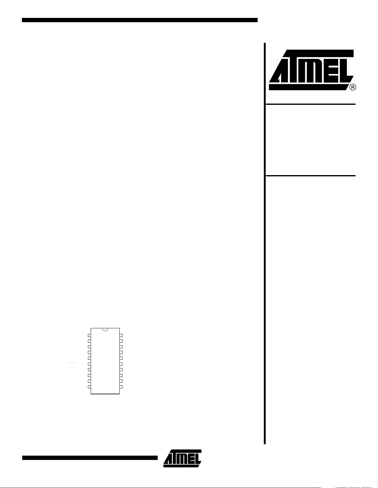
Pin Configuration
PDIP/SOIC
RST/VPP
(RXD) P3.0
(TXD) P3.1
XTAL2
XTAL1
(INT0) P3.2
(INT1) P3.3
(TO) P3.4
(T1) P3.5
GND
1
2
3
4
5
6
7
8
9
10
20
19
18
17
16
15
14
13
12
11
VCC
P1.7
P1.6
P1.5
P1.4
P1.3
P1.2
P1.1 (AIN1)
P1.0 (AIN0)
P3.7
Flash
AT89C2051
Rev. 0368E–02/00
1
Page 2
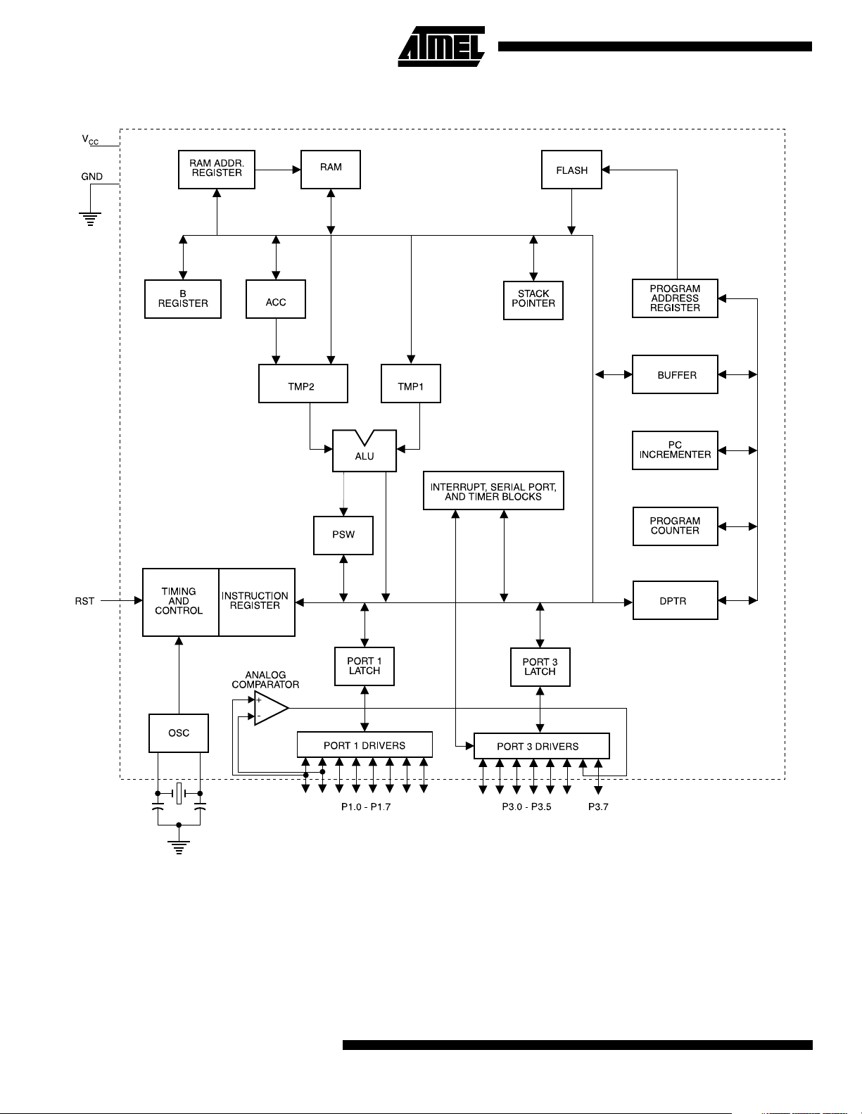
Block Diagram
2
AT89C2051
Page 3
AT89C2051
Pin Description
VCC
Supply voltage.
GND
Ground.
Port 1
Port 1 is an 8-bit bi-irectional I/O port. Port pins P1.2 to
P1.7 provide internal pullups. P1.0 and P1.1 require external pullups. P1.0 and P1.1 also serve as the positive input
(AIN0) and the negative input (AIN1), respectively, of the
on-chip precision analog comparator. The Port 1 output
buffers can sink 20 mA and can drive LED displays directly.
When 1s are written to Port 1 pins, they can be used as
inputs. When pins P1.2 to P1.7 are used as inputs and are
externally pulled low, they will source current (I
of the internal pullups.
Port 1 also receives code data during Flash programming
and verification.
Port 3
Port 3 pins P3.0 to P3.5, P3.7 are seven bi-irectional I/O
pins with internal pullups. P3.6 is hard-wired as an input to
the output of the on-chip comparator and is not accessible
as a general purpose I/O pin. The Port 3 output buffers can
sink 20 mA. When 1s are written to Port 3 pins they are
pulled high by the internal pullups and can be used as
inputs. As inputs, Port 3 pins that are externally being
pulled low will source current (I
) because of the pullups.
IL
Port 3 also serves the functions of various special features
of the AT89C2051 as listed below:
) because
IL
Each machine cycle takes 12 oscillator or clock cycles.
XTAL1
Input to the inverting oscillator amplifier and input to the
internal clock operating circuit.
XTAL2
Output from the inverting oscillator amplifier.
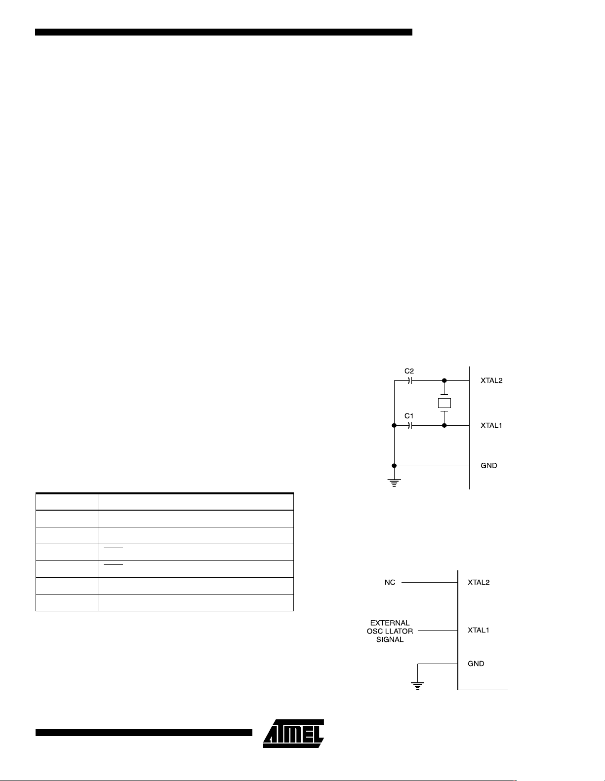
Oscillator Characteristics
XTAL1 and XTAL2 are the input and output, respectively,
of an inverting amplifier which can be configured for use as
an on-chip oscillator, as shown in Figure 1. Either a quartz
crystal or ceramic resonator may be used. To drive the
device from an external clock source, XTAL2 should be left
unconnected while XTAL1 is driven as shown in Figure 2.
There are no requirements on the duty cycle of the external
clock signal, since the input to the internal clocking circuitry
is through a divide-by-two flip-flop, but minimum and maximum voltage high and low time specifications must be
observed.
Figure 1. Oscillator Connections
Port Pin Alternate Functions
P3.0 RXD (serial input port)
P3.1 TXD (serial output port)
P3.2 INT0
P3.3 INT1
P3.4 T0 (timer 0 external input)
P3.5 T1 (timer 1 external input)
(external interrupt 0)
(external interrupt 1)
Port 3 also receives some control signals for Flash programming and verification.
RST
Reset input. All I/O pins are reset to 1s as soon as RST
goes high. Holding the RST pin high for two machine
cycles while the oscillator is running resets the device.
Note: C1, C2 = 30 pF ± 10 pF for Crystals
= 40 pF ± 10 pF for Ceramic Resonators
Figure 2. External Clock Drive Configuration
3
Page 4

Special Function Registers
A map of the on-chip memory area called the Special Function Register (SFR) space is shown in the table below.
Note that not all of the addresses are occupied, and unoccupied addresses may not be implemented on the chip.
Read accesses to these addresses will in general return
random data, and write accesses will have an indeterminate effect.
User software should not write 1s to these unlisted locations, since they may be used in future products to invoke
new features. In that case, the reset or inactive values of
the new bits will always be 0.
Table 1. AT89C2051 SFR Map and Reset Values
0F8H 0FFH
0F0H B
00000000
0E8H 0EFH
0E0H ACC
00000000
0D8H 0DFH
0D0H PSW
00000000
0C8H 0CFH
0F7H
0E7H
0D7H
0C0H 0C7H
0B8H IP
XXX00000
0B0H P3
11111111
0A8H IE
0XX00000
0A0H 0A7H
98H SCON
00000000
90H P1
11111111
88H TCON
00000000
80H SP
SBUF
XXXXXXXX
TMOD
00000000
00000111
TL0
00000000
DPL
00000000
TL1
00000000
DPH
00000000
TH0
00000000
TH1
00000000
PCON
0XXX0000
0BFH
0B7H
0AFH
9FH
97H
8FH
87H
4
AT89C2051
Page 5
AT89C2051
Restrictions on Certain Instructions
The AT89C2051 and is an economical and cost-effective
member of Atmel’s growing family of microcontrollers. It
contains 2K bytes of flash program memory. It is fully compatible with the MCS-51 architecture, and can be
programmed using the MCS-51 instruction set. However,
there are a few considerations one must keep in mind
when utilizing certain instructions to program this device.
All the instructions related to jumping or branching should
be restricted such that the destination address falls within
the physical program memory space of the device, which is
2K for the AT89C2051. This should be the responsibility of
the software programmer. For example, LJMP 7E0H
would be a valid instruction for the AT89C2051 (with 2K of
memory), whereas LJMP 900H would not.
1. Branching instructions:
LCALL, LJMP, ACALL, AJMP, SJMP, JMP @A+DPTR
These unconditional branching instructions will execute
correctly as long as the programmer keeps in mind that the
destination branching address must fall within the physical
boundaries of the program memory size (locations 00H to
7FFH for the 89C2051). Violating the physical space limits
may cause unknown program behavior.
CJNE [...], DJNZ [...], JB, JNB, JC, JNC, JBC, JZ, JNZ With
these conditional branching instructions the same rule
above applies. Again, violating the memory boundaries
may cause erratic execution.
For applications involving interrupts the normal interrupt
service routine address locations of the 80C51 family architecture have been preserved.
2. MOVX-related instructions, Data Memory:
The AT89C2051 contains 128 bytes of internal data memory. Thus, in the AT89C2051 the stack depth is limited to
128 bytes, the amount of available RAM. External DATA
memory access is not supported in this device, nor is external PROGRAM memory execution. Therefore, no MOVX
[...] instructions should be included in the program.
A typical 80C51 assembler will still assemble instructions,
even if they are written in violation of the restrictions mentioned above. It is the responsibility of the controller user to
know the physical features and limitations of the device
being used and adjust the instructions used
correspondingly.
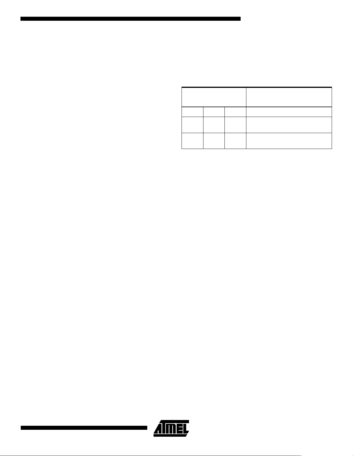
Program Memory Lock Bits
On the chip are two lock bits which can be left unprogrammed (U) or can be programmed (P) to obtain the
additional features listed in the table below:
Lock Bit Protection Modes
Program Lock Bits
LB1 LB2 Protection Type
1 U U No program lock features.
2 P U Further programming of the Flash
is disabled.
3 P P Same as mode 2, also verify is
disabled.
Note: 1. The Lock Bits can only be erased with the Chip Erase
operation.
(1)
Idle Mode
In idle mode, the CPU puts itself to sleep while all the onchip peripherals remain active. The mode is invoked by
software. The content of the on-chip RAM and all the special functions registers remain unchanged during this
mode. The idle mode can be terminated by any enabled
interrupt or by a hardware reset.
P1.0 and P1.1 should be set to “0” if no external pullups are
used, or set to “1” if external pullups are used.
It should be noted that when idle is terminated by a hardware reset, the device normally resumes program
execution, from where it left off, up to two machine cycles
before the internal reset algorithm takes control. On-chip
hardware inhibits access to internal RAM in this event, but
access to the port pins is not inhibited. To eliminate the
possibility of an unexpected write to a port pin when Idle is
terminated by reset, the instruction following the one that
invokes Idle should not be one that writes to a port pin or to
external memory.
Power-down Mode
In the power down mode the oscillator is stopped, and the
instruction that invokes power down is the last instruction
executed. The on-chip RAM and Special Function Registers retain their values until the power down mode is
terminated. The only exit from power down is a hardware
reset. Reset redefines the SFRs but does not change the
on-chip RAM. The reset should not be activated before V
is restored to its normal operating level and must be held
active long enough to allow the oscillator to restart and
stabilize.
P1.0 and P1.1 should be set to “0” if no external pullups are
used, or set to “1” if external pullups are used.
CC
5
Page 6

Programming The Flash
The AT89C2051 is shipped with the 2K bytes of on-chip
PEROM code memory array in the erased state (i.e., contents = FFH) and ready to be programmed. The code
memory array is programmed one byte at a time. Once the
array is programmed, to re-program any non-blank byte,
the entire memory array needs to be erased electrically.
Internal Address Counter: The AT89C2051 contains an
internal PEROM address counter which is always reset to
000H on the rising edge of RST and is advanced by applying a positive going pulse to pin XTAL1.
Programming Algorithm: To program the AT89C2051,
the following sequence is recommended.
1. Power-up sequence:
Apply power between V
Set RST and XTAL1 to GND
2. Set pin RST to “H”
Set pin P3.2 to “H”
3. Apply the appropriate combination of “H” or “L” logic
levels to pins P3.3, P3.4, P3.5, P3.7 to select one of the
programming operations shown in the PEROM Programming Modes table.
To Program and Verify the Array:
4. Apply data for Code byte at location 000H to P1.0 to
P1.7.
5. Raise RST to 12V to enable programming.
6. Pulse P3.2 once to program a byte in the PEROM array
or the lock bits. The byte-write cycle is self-timed and
typically takes 1.2 ms.
7. To verify the programmed data, lower RST from 12V to
logic “H” level and set pins P3.3 to P3.7 to the appropiate
levels. Output data can be read at the port P1 pins.
8. To program a byte at the next address location, pulse
XTAL1 pin once to advance the internal address
counter. Apply new data to the port P1 pins.
9. Repeat steps 5 through 8, changing data and advancing
the address counter for the entire 2K bytes array or until
the end of the object file is reached.
10.Power-off sequence:
set XTAL1 to “L”
set RST to “L”
Turn V
Data
Polling: The AT89C2051 features Data Polling to
indicate the end of a write cycle. During a write cycle, an
attempted read of the last byte written will result in the complement of the written data on P1.7. Once the write cycle
has been completed, true data is valid on all outputs, and
power off
CC
and GND pins
CC
the next cycle may begin. Data
after a write cycle has been initiated.
Ready/Busy
be monitored by the RDY/BSY
pulled low after P3.2 goes High during programming to indicate BUSY. P3.1 is pulled High again when programming is
done to indicate READY.
Program Verify: If lock bits LB1 and LB2 have not been
programmed code data can be read back via the data lines
for verification:
1. Reset the internal address counter to 000H by bringing
RST from “L” to “H”.
2. Apply the appropriate control signals for Read Code data
and read the output data at the port P1 pins.
3. Pulse pin XTAL1 once to advance the internal address
counter.
4. Read the next code data byte at the port P1 pins.
5. Repeat steps 3 and 4 until the entire array is read.
The lock bits cannot be verified directly. Verification of the
lock bits is achieved by observing that their features are
enabled.
Chip Erase: The entire PEROM array (2K bytes) and the
two Lock Bits are erased electrically by using the proper
combination of control signals and by holding P3.2 low for
10 ms. The code array is written with all “1”s in the Chip
Erase operation and must be executed before any nonblank memory byte can be re-programmed.
Reading the Signature Bytes: The signature bytes are
read by the same procedure as a normal verification of
locations 000H, 001H, and 002H, except that P3.5 and
P3.7 must be pulled to a logic low. The values returned are
as follows.
(000H) = 1EH indicates manufactured by Atmel
(001H) = 21H indicates 89C2051
: The Progress of byte programming can also
Polling may begin any time
output signal. Pin P3.1 is
Programming Interface
Every code byte in the Flash array can be written and the
entire array can be erased by using the appropriate combination of control signals. The write operation cycle is selftimed and once initiated, will automatically time itself to
completion.
All major programming vendors offer worldwide support for
the Atmel microcontroller series. Please contact your local
programming vendor for the appropriate software revision.
6
AT89C2051
Page 7

AT89C2051
PP
Flash Programming Modes
Mode RST/VPP P3.2/PROG P3.3 P3.4 P3.5 P3.7
Write Code Data
(1)(3)
12V L H H H
Read Code Data
Write Lock Bit - 1 12V H H H H
Chip Erase 12V H L L L
Read Signature Byte H H L L L L
Notes: 1. The internal PEROM address counter is reset to 000H on the rising edge of RST and is advanced by a positive pulse at
2. Chip Erase requires a 10 ms PROG
3. P3.1 is pulled Low during programming to indicate RDY/BSY
(1)
XTAL 1 pin.
HHLLHH
Bit - 2 12V H H L L
(2)
pulse.
.
Figure 3. Programming the Flash Memory Figure 4. Verifying the Flash Memory
7
Page 8

Flash Programming and Verification Characteristics
TA = 0°C to 70°C, VCC = 5.0 ± 10%
Symbol Parameter Min Max Units
V
PP
I
PP
t
DVGL
t
GHDX
t
EHSH
t
SHGL
t
GHSL
t
GLGH
t
ELQV
t
EHQZ
t
GHBL
t
WC
t
BHIH
t
IHIL
Programming Enable Voltage 11.5 12.5 V
Programming Enable Current 250 µA
Data Setup to PROG Low 1.0 µs
Data Hold after PROG 1.0 µs
P3.4 (ENABLE) High to V
PP
VPP Setup to PROG Low 10 µs
VPP Hold after PROG 10 µs
PROG Width 1 110 µs
ENABLE Low to Data Valid 1.0 µs
Data Float after ENABLE 01.0 µs
PROG High to BUSY Low 50 ns
Byte Write Cycle Time 2.0 ms
RDY/BSY\ to Increment Clock Delay 1.0 µs
Increment Clock High 200 ns
Note: 1. Only used in 12-volt programming mode.
Flash Programming and Verification Waveforms
1.0 µs
8
AT89C2051
Page 9

AT89C2051
Absolute Maximum Ratings*
Operating Temperature ................................. -55°C to +125°C
Storage Temperature..................................... -65°C to +150°C
Voltage on Any Pin
with Respect to Ground.....................................-1.0V to +7.0V
Maximum Operating Voltage ............................................ 6.6V
DC Output Current...................................................... 25.0 mA
DC Characteristics
TA = -40°C to 85°C, VCC = 2.0V to 6.0V (unless otherwise noted)
Symbol Parameter Condition Min Max Units
*NOTICE: Stresses beyond those listed under “Absolute
Maximum Ratings” may cause permanent damage to the device. This is a stress rating only and
functional operation of the device at these or any
other conditions beyond those indicated in the
operational sections of this specification is not
implied. Exposure to absolute maximum rating
conditions for extended periods may affect device
reliability.
V
IL
V
IH
V
IH1
V
OL
V
OH
I
IL
Input Low-voltage -0.5 0.2 V
Input High-voltage (Except XTAL1, RST) 0.2 V
Input High-voltage (XTAL1, RST) 0.7 V
Output Low-voltage
(Ports 1, 3)
Output High-voltage
(Ports 1, 3)
Logical 0 Input Current
(1)
IOL = 20 mA, VCC = 5V
I
= 10 mA, VCC = 2.7V
OL
IOH = -80 µA, VCC = 5V ± 10% 2.4 V
IOH = -30 µA 0.75 V
I
= -12 µA 0.9 V
OH
VIN = 0.45V -50 µA
+ 0.9 V
CC
CC
CC
CC
CC
V
CC
- 0.1 V
CC
+ 0.5 V
+ 0.5 V
0.5 V
(Ports 1, 3)
I
TL
Logical 1 to 0 Transition Current
VIN = 2V, VCC = 5V ± 10% -750 µA
(Ports 1, 3)
I
LI
Input Leakage Current
0 < VIN < V
CC
±10 µA
(Port P1.0, P1.1)
V
OS
V
CM
Comparator Input Offset Voltage VCC = 5V 20 mV
Comparator Input Common
0VCCV
Mode Voltage
RRST Reset Pull-down Resistor 50 300 KΩ
C
IO
I
CC
Pin Capacitance Test Freq. = 1 MHz, TA = 25°C10pF
Power Supply Current Active Mode, 12 MHz, VCC = 6V/3V 15/5.5 mA
Power-down Mode
Idle Mode, 12 MHz, V
P1.0 & P1.1 = 0V or V
(2)
VCC = 6V P1.0 & P1.1 = 0V or V
VCC = 3V P1.0 & P1.1 = 0V or V
= 6V/3V
CC
CC
CC
CC
5/1 mA
100 µA
20 µA
Notes: 1. Under steady state (non-transient) conditions, IOL must be externally limited as follows:
Maximum I
Maximum total I
exceeds the test condition, VOL may exceed the related specification. Pins are not guaranteed to sink current greater
If I
OL
per port pin: 20 mA
OL
for all output pins: 80 mA
OL
than the listed test conditions.
2. Minimum VCC for Power-down is 2V.
V
V
9
Page 10

External Clock Drive Waveforms
External Clock Drive
Symbol Parameter
VCC = 2.7V to 6.0V VCC = 4.0V to 6.0V
UnitsMin Max Min Max
1/t
t
CLCL
t
CHCX
t
CLCX
t
CLCH
t
CHCL
CLCL
Oscillator Frequency 0 12 0 24 MHz
Clock Period 83.3 41.6 ns
High Time 30 15 ns
Low Time 30 15 ns
Rise Time 20 20 ns
Fall Time 20 20 ns
10
AT89C2051
Page 11

()
Serial Port Timing: Shift Register Mode Test Conditions
VCC = 5.0V ± 20%; Load Capacitance = 80 pF
12 MHz Osc Variable Oscillator
AT89C2051
Symbol Parameter
t
XLXL
t
QVXH
t
XHQX
t
XHDX
t
XHDV
Serial Port Clock Cycle Time 1.0 12t
Output Data Setup to Clock Rising Edge 700 10t
Output Data Hold after Clock Rising Edge 50 2t
Input Data Hold after Clock Rising Edge 0 0 ns
Clock Rising Edge to Input Data Valid 700 10t
Shift Register Mode Timing Waveforms
CLCL
-133 ns
CLCL
-117 ns
CLCL
-133 ns
CLCL
UnitsMin Max Min Max
µs
AC Testing Input/Output Waveforms
(1)
Note: 1. AC Inputs during testing are driven at VCC - 0.5V for a
logic 1 and 0.45V for a logic 0. Timing measurements
are made at V
min. for a logic 1 and VIL max. for a
IH
logic 0.
Float Waveforms
(1)
Note: 1. For timing purposes, a port pin is no longer floating
when a 100 mV change from load voltage occurs. A
port pin begins to float when 100 mV change frothe
loaded V
OH/VOL
level occurs.
11
Page 12

AT89C2051
TYPICAL ICC - ACTIVE (85°C)
20
15
I
C
C
10
m
5
A
0
0 6 12 18 24
Vcc= 5.0V
Vcc= 6.0V
Vcc= 3.0V
FREQUENCY (MHz)
AT89C2051
TYPICAL ICC - IDLE (85°C)
3
I
2
C
C
1
m
A
0
036912
FREQUENCY (MHz)
Vcc= 5.0V
Vcc= 6.0V
Vcc= 3.0V
12
AT89C2051
TYPICAL ICC vs. VOLTAGE- POWER DOWN (85°C)
20
15
I
C
C
10
µ
5
A
0
3.0V 4.0V 5.0V 6.0V
Vcc VOLTAGE
Notes: 1. XTAL1 tied to GND for ICC (power-down)
2. P.1.0 and P1.1 = V
or GND
CC
3. Lock bits programmed
AT89C2051
Page 13

Ordering Information
AT89C2051
Speed
(MHz)
12 2.7V to 6.0V AT89C2051-12PC
24 4.0V to 6.0V AT89C2051-24PC
Power
Supply Ordering Code Package Operation Range
AT89C2051-12SC
AT89C2051-12PI
AT89C2051-12SI
AT89C2051-24SC
AT89C2051-24PI
AT89C2051-24SI
20P3
20S
20P3
20S
20P3
20S
20P3
20S
Commercial
(0°C to 70°C)
Industrial
(-40°C to 85°C)
Commercial
(0°C to 70°C)
Industrial
(-40°C to 85°C)
Package Type
20P3 20-lead, 0.300” Wide, Plastic Dual In-line Package (PDIP)
20S 20-lead, 0.300” Wide, Plastic Gull Wing Small Outline (SOIC)
13
Page 14

Packaging Information
20P3, 20-lead, 0.300" Wide, Plastic Dual Inline
Package (PDIP)
Dimensions in Inches and (Millimeters)
JEDEC STANDARD MS-001 AD
1.060(26.9)
.210(5.33)
SEATING
PLANE
.980(24.9)
.900(22.86) REF
MAX
.150(3.81)
.115(2.92)
.110(2.79)
.090(2.29)
.014(.356)
.008(.203)
PIN
1
.070(1.78)
.045(1.13)
.325(8.26)
.300(7.62)
0
REF
15
.430(10.92) MAX
.090(2.29)
.005(.127)
.015(.381) MIN
.022(.559)
.014(.356)
.280(7.11)
.240(6.10)
MAX
MIN
20S, 20-lead, 0.300" Wide, Plastic Gull WIng Small
Outline (SOIC)
Dimensions in Inches and (Millimeters)
0.020 (0.508)
0.013 (0.330)
0.420 (10.7)
0.299 (7.60)
0.393 (9.98)
0.012 (0.305)
0.003 (0.076)
0.291 (7.39)
0.013 (0.330)
0.009 (0.229)
0.105 (2.67)
0.092 (2.34)
PIN 1
0
8
REF
0.035 (0.889)
0.015 (0.381)
.050 (1.27) BSC
0.513 (13.0)
0.497 (12.6)
14
AT89C2051
Page 15

Atmel Headquarters Atmel Operations
Corporate Headquarters
2325 Orchard Parkway
San Jose, CA 95131
TEL (408) 441-0311
FAX (408) 487-2600
Europe
Atmel U.K., Ltd.
Coliseum Business Centre
Riverside Way
Camberley, Surrey GU15 3YL
England
TEL (44) 1276-686-677
FAX (44) 1276-686-697
Asia
Atmel Asia, Ltd.
Room 1219
Chinachem Golden Plaza
77 Mody Road Tsimhatsui
East Kowloon
Hong Kong
TEL (852) 2721-9778
FAX (852) 2722-1369
Japan
Atmel Japan K.K.
9F, Tonetsu Shinkawa Bldg.
1-24-8 Shinkawa
Chuo-ku, Tokyo 104-0033
Japan
TEL (81) 3-3523-3551
FAX (81) 3-3523-7581
Atmel Colorado Springs
1150 E. Cheyenne Mtn. Blvd.
Colorado Springs, CO 80906
TEL (719) 576-3300
FAX (719) 540-1759
Atmel Rousset
Zone Industrielle
13106 Rousset Cedex
France
TEL (33) 4-4253-6000
FAX (33) 4-4253-6001
Fax-on-Demand
North America:
1-(800) 292-8635
International:
1-(408) 441-0732
e-mail
literature@atmel.com
Web Site
http://www.atmel.com
BBS
1-(408) 436-4309
© Atmel Corporation 2000.
Atmel Corporation makes no warranty for the use of its products, other than those expressly contained in the Company’s standard warranty which is detailed in Atmel’s Terms and Conditions located on the Company’s web site. The Company assumes no responsibility for
any errors which may appear in this document, reserves the right to change devices or specifications detailed herein at any time without
notice, and does not make any commitment to update the information contained herein. No licenses to patents or other intellectual property of Atmel are granted by the Company in connection with the sale of Atmel products, expressly or by implication. Atmel’s products are
not authorized for use as critical components in life support devices or systems.
Marks bearing ® and/or ™ are registered trademarks and trademarks of Atmel Corporation.
Terms and product names in this document may be trademarks of others.
Printed on recycled paper.
0368E–02/00/xM
 Loading...