

Page 1
Features
•
Compatible with MCS-51™ Products
•
8K Bytes of Reprogrammable Flash Memory
– Endurance: 1,000 Write/Erase Cycles
•
2.7V to 6V Operating Range
•
Fully Static Operation: 0 Hz to 12 MHz
•
Three-Level Program Memory Lock
•
256 x 8-Bit Internal RAM
•
32 Programmable I/O Lines
•
Three 16-Bit Timer/Counters
•
Eight Interrupt Sources
•
Programmable Serial Channel
•
Low Power Idle and Power Down Modes
8-Bit
Microcontroller
Description
The AT89LV52 is a low-voltage, high-performance CMOS 8-bit microcomputer with
8K bytes of Flash programmable and erasable read only memory. The device is manufactured using Atmel’s high density nonvolatile memory technology and is compatible with the industry standard 80C51 and 80C52 instruction set and pinout. The onchip Flash allows the p rogram memor y to be repr ogrammed in- system or by a conventional nonvolatile memory programmer. By combi ning a versati le 8-bit CPU with
Flash on a monolithic chip, the Atmel AT89LV52 is a powerful microcomputer which
provides a highly flex ible and co st effe ctive solu tion to many embedd ed con trol app lications. The AT89LV52 operates at 2.7 volts up to 6.0 volts.
(continued)
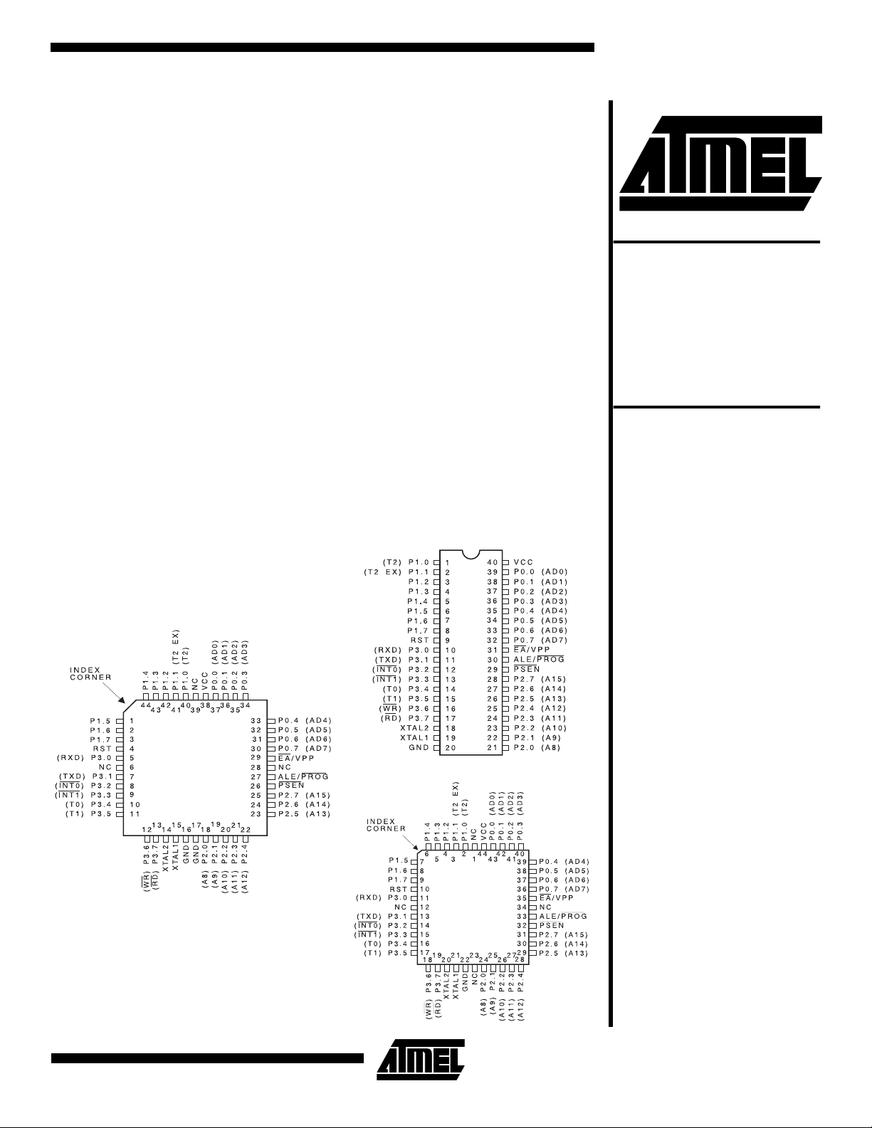
Pin Configurations
TQFP
PDIP
with 8K Bytes
Flash
AT89LV52
PLCC
0375D-E–12/97
4-83
Page 2
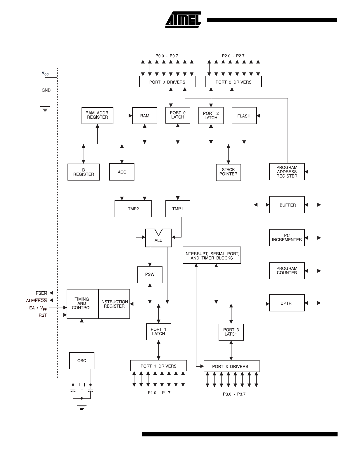
Block Diagram
4-84
AT89LV52
Page 3
AT89LV52
The AT89LV52 provides the following standard features:
8K bytes of Flash, 256 bytes of RAM, 32 I/O lines, three 16bit timer/counters, a six-vector two-level interrupt architecture, a full duplex serial port, on -chip oscillat or, and clock
circuitry. In addition, the AT89LV52 is designed with static
logic for operation down to zero frequency an d supports
two software select able power saving mo des. The Idle
Mode stops the CPU while allowing the RAM,
timer/counters, serial p or t, and int er rupt s yst em to co nti nue
functioning. The Power Down Mode saves the RAM contents but freezes the oscillator, disabling all other chip functions until the next hardware reset.
Pin Description
V
CC
Supply voltage.
GND
Ground.
Port 0
Port 0 is an 8-bit open drain bidirectional I/O port. As an
output port, each pin can sink eight TTL inputs. When 1s
are written to port 0 pins, the pins can be used as highimpedance inputs.
Port 0 can also be configu red to be the multiplex ed loworder address/data bus during accesses to ex ternal program and data memory. In this mode, P0 has internal pullups.
Port 0 also rece ives th e code by tes dur ing Fla sh prog ramming and outputs the code bytes during program ver ification. External pu llups are requ ired during pr ogram v erific ation.
Port 1
Port 1 is an 8-bit bidire ction al I/O por t w ith inter nal pullu ps.
The Port 1 output buffers can sink/source four TTL inputs.
When 1s are written to Port 1 pins , they are p ulled hi gh by
the internal pullups and can be used as inputs. As inputs ,
Port 1 pins that are externally being pulled low will source
current (I
In addition, P1.0 and P1. 1 can be configured to be the
timer/counter 2 external count input (P1.0/T2) and the
timer/counter 2 trigger input (P1.1/T2EX), respectively, as
shown in the following table.
Port Pin Alternate Functions
P1.0 T2 (external count input to
P1.1 T2EX (Timer/Counter 2 capture/reload
Port 1 also receives the low-order address bytes during
Flash programming and verification.
) because of the internal pullups.
IL
Timer/Counter 2), clock-out
trigger and direction control)
Port 2
Port 2 is an 8-bit bidirectional I/O port with interna l pullups.
The Port 2 output buffers can sink/source four TTL inputs.
When 1s are writte n to Po rt 2 pi ns, they a re pul led high by
the internal pullups and can be used as inputs. As inputs,
Port 2 pins that are externally being pulled low will source
current (I
) because of the internal pullups.
IL
Port 2 emits the high-order address byte during fetches
from external program memory and during accesses to
external data memory th at u se 16 -b it a ddres s es ( MO VX @
DPTR). In this application, Port 2 uses strong internal pullups when emitting 1s. During accesses to external data
memory that use 8-bit addresses (MOVX @ RI), Port 2
emits the contents of the P2 Special Function Register.
Port 2 also receives the high-order address bits and some
control signals during Flash programming and verification.
Port 3
Port 3 is an 8-bit bidirectional I/O port with interna l pullups.
The Port 3 output buffers can sink/source four TTL inputs.
When 1s are writte n to Po rt 3 pi ns, they a re pul led high by
the internal pullups and can be used as inputs. As inputs,
Port 3 pins that are externally being pulled low will source
current (I
) because of the pullups.
IL
Port 3 also serv es t he fun ctions of v arious spe cial f eatures
of the AT89LV51, as shown in the following table.
Port Pin Alternate Functions
P3.0 RXD (serial input port)
P3.1 TXD (serial output port)
P3.2 INT0 (external interrupt 0)
P3.3 INT1
P3.4 T0 (timer 0 external input)
P3.5 T1 (timer 1 external input)
P3.6 WR
P3.7 RD
(external interrupt 1)
(external data memory write strobe)
(external data memory read strobe)
Port 3 also receives some control signals for Flash programming and verification.
RST
Reset input. A high on this pin for two machine cycles while
the oscillator is running resets the device.
ALE/PROG
Address Latch Enable is an output pulse for latching the
low byte of the address during accesses to external memory. This pi n is al so t h e pr og ra m pu l se in p ut (PROG
) during
Flash programming.
In normal operation, ALE is emitted at a constant rate of 1/6
the oscillator frequency and may be used for external timing or clocking purposes. Note, however, that one ALE
4-85
Page 4

pulse is skipped durin g each access to exte rnal data me mory.
If desired, ALE operation can be disabled by setting bit 0 of
SFR location 8EH. With the bit set, ALE is active only during a MOVX or MOVC instruction. Otherwise, the pin is
weakly pulled high. Setting the ALE-disable bit has no
effect if the microcontroller is in external execution mode.
PSEN
Program Store Enable is the read strobe to external pro-
gram memory.
When the AT89LV52 is executing code from external pro-
gram memory, PSEN
cycle, except that two PSEN
is activated twice each machine
activations are skipped during
each access to external data memory.
/V
EA
PP
External Access Enable. EA must be strapped to GN D in
order to enable the device to fetch code from external program memory locations starting at 0000H up to FFFFH.
Note, however, that if lock bit 1 is programmed, EA
will be
internally latched on reset.
should be strapped to VCC for internal program execu-
EA
tions.
This pin also receives the 12-volt programming enable voltage (V
) during Flash programming when 12-volt pro-
PP
gramming is selected.
XTAL1
Input to the inverting oscillator am plifier and input to the
internal clock operating circuit.
XTAL2
Output from the inverting oscillator amplifier.
Table 1.
0D8H 0DFH
0D0H PSW
0C8H T2CON
0C0H 0C7H
0B8H IP
0B0H P3
0A8H IE
0A0H P2
AT89LV52 SFR Map and Reset Values
0F8H 0FFH
0F0H
0E8H 0EFH
0E0H ACC
98H SCON
90H P1
88H TCON
80H P0
B
00000000
00000000
00000000
00000000
XX000000
11111111
0X000000
11111111
00000000
11111111
00000000
11111111
T2MOD
XXXXXX00
SBUF
XXXXXXXX
TMOD
00000000
SP
00000111
RCAP2L
00000000
TL0
00000000
DPL
00000000
RCAP2H
00000000
TL1
00000000
DPH
00000000
TL2
00000000
TH0
00000000
TH2
00000000
TH1
00000000
PCON
0XXX0000
0F7H
0E7H
0D7H
0CFH
0BFH
0B7H
0AFH
0A7H
9FH
97H
8FH
87H
4-86
AT89LV52
Page 5
AT89LV52
Special Function Registers
A map of the on-chip memory area called the Special Function Register (SFR) space is shown in Table 1.
Note that not all of the addresses are occupied, and unoccupied addresses may not be implemented on the chip.
Read accesses to these addresses will in general return
random data, and write accesses will have an indeterminate effect.
User software should not write 1s to these unlisted locations, since they may be used in future products to invoke
Table 2.
T2CON Address = 0C8H Reset Value = 0000 0000B
Bit Addressable
Symbol Function
TF2 Timer 2 overflow flag set by a Timer 2 overflow and must be cleared by software. TF2 will not be set when either
EXF2 Timer 2 external flag set whe n either a capture or reloa d is c aused b y a negat iv e tr ans ition on T2 EX and EXEN2 = 1.
T2CON—Timer/Counter 2 Control Register
TF2 EXF2 RCLK TCLK EXEN2 TR2 C/T2
Bit76543210
RCLK = 1 or TCLK = 1.
When Timer 2 interrupt is enabled, EXF2 = 1 will cause the CPU to vector to the Timer 2 interrupt routine. EXF2
must be cleared by software. EXF2 does not cause an interrupt in up/down counter mode (DCEN = 1).
new features. In th at case, th e reset or inac tive valu es of
the new bits will always be 0.
Timer 2 Registers
Control and status bits are contained in
registers T2CON (shown in Table 2) and T2MOD (shown in
Table 4) for Timer 2. The register pair (RCAP2H, RCA P2L )
are the Capture/ Reloa d regist ers for Timer 2 i n 16-bit c apture mode or 16-bit auto-reload mode.
Interrupt Registers
The individual interrupt enable b its
are in the IE register. Two priorities can be set for each of
the six interrupt sources in the IP register.
CP/RL2
RCLK Receive clock enable. When set, causes the serial port to use Timer 2 overflow pulses for its receive clock in serial
port Modes 1 and 3. RCLK = 0 causes Timer 1 overflow to be used for the receive clock.
TCLK Transmit clock enable. Wh en set, causes the serial port to use Timer 2 overflow pulses for its transmit clock in serial
port Modes 1 and 3. TCLK = 0 causes Timer 1 overflows to be used for the transmit clock.
EXEN2 Timer 2 external ena ble. When set, al lows a capture or reload to oc cu r as a re sult o f a neg ati ve transition o n T2 EX if
Timer 2 is not being used to clock the serial port. EXEN2 = 0 causes Timer 2 to ignore events at T2EX.
TR2 Start/Stop control for Timer 2. TR2 = 1 starts the timer.
C/T2
CP/RL2
Data Memory
The AT89LV52 implements 256 bytes of on-chip RAM. The
upper 128 bytes oc cupy a parallel ad dress space to the
Special Function Register s. That means the u pper 128
bytes have the same addresses as the SFR space but are
physically separate from SFR space.
When an instruction accesses an internal location above
address 7FH, the address mode used in the instruction
specifies whether the CPU accesses the upper 128 bytes
of RAM or the SFR space. Instructions that use direct
addressing access SFR space.
Timer or counter select for Timer 2. C/T2 = 0 for timer function. C/T2 = 1 for external event counter (falling edge
triggered).
Capture/Reload select. CP/RL2 = 1 causes captures to occur on negative transitio ns at T2EX if EXEN2 = 1. CP/RL2
= 0 causes automatic reloads to o ccur when Ti mer 2 o v erflo ws o r negati ve tran sitions o ccur at T2EX whe n EXEN2 =
1. When either RCLK or TCLK = 1, this bit is ignored and the timer is forced to auto-reload on Timer 2 overflow.
For example, the following direct addressing instruction
accesses the SFR at location 0A0H (which is P2).
MOV 0A0H, #data
Instructions that use indirect addressing access the upper
128 bytes of RAM. For example, the following indirect
addressing inst ructi on, where R0 contains 0A 0H, accesses
the data byte at address 0A0H, rather than P2 (whose
address is 0A0H).
MOV @R0, #data
Note that stack operations are examples of indirect
addressing, so the upper 128 bytes of data RAM are avail able as stack space.
4-87
Page 6
Timer 0 and 1
Timer 0 and Timer 1 in the AT89LV52 operate the same
way as Timer 0 and Timer 1 in the AT89LV51.
Timer 2
Timer 2 is a 16-bit Timer/Counter that can operate as either
a timer or an event counter. The type of operation is
selected by bit C/T2
Timer 2 has three operating modes: capture, auto-reload
(up or down counting), and baud rate generator. The
modes are selected by bits in T2CON, as shown in Table 3.
Timer 2 consists of two 8- bi t regi st er s, TH2 and TL2. I n the
Timer function, the TL2 r egister is incremented ever y
machine cycle. Since a machine cycle consists of 12 oscillator periods, the count rate is 1/12 of the oscillator frequency.
In the Counter function, the register is incremented in
response to a 1-to-0 transition at its corresponding external
input pin, T2. In thi s func tion, the extern al i nput is sa mpled
in the SFR T2 C ON (sh o w n i n Ta bl e 2).
during S5P2 of every machine cy cle. When the sampl es
show a high in one cycle and a low in the next cycle, the
count is incremented. The new count value appears in the
register during S3P1 of the cycle following the one in which
the transition was detected. Since two machine cycles (24
oscillator perio ds ) ar e re qui red to recognize a 1 -to -0 tr an si tion, the maximum count rate is 1/24 of the oscillator frequency. To ensure that a given level is sampled at least
once before it changes, the level should be held for at least
one full machine cycle.
Table 3.
RCLK + TCLK CP/RL2 TR2 MODE
Timer 2 Operating Modes
0 0 1 16-Bit Auto-Reload
0 1 1 16-Bit Capture
1 X 1 Baud Rate Generator
XX0(Off)
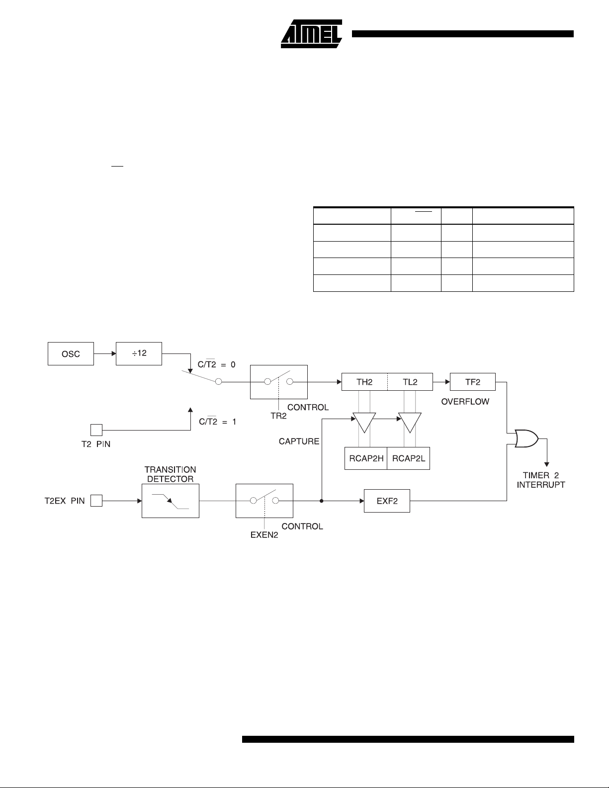
Figure 1.
Timer 2 in Capture Mode
Capture Mode
In the capture mode, two option s are selected by bit
EXEN2 in T2CON. If EXEN2 = 0, Timer 2 is a 16-bit timer
or counter which upon overflow sets bit TF2 in T2CON.
This bit can then be used to generate an interrupt. If
EXEN2 = 1, Timer 2 performs the s ame oper ation, but a 1to-0 transition at external input T2EX also causes the current value in TH2 and TL2 to be captured into RCAP2H and
RCAP2L, resp ective ly. In add ition, th e transi tion at T2E X
causes bit EXF2 in T2CON to b e set. The EX F2 bit, like
TF2, can generate an interrupt. The capture mode is illustrated in Figure 1.
Auto-Reload (Up or Down Counter)
Timer 2 can be programmed to count up or down when
configured in its 16-bit auto-reload mode. This feature is
invoked by the DCEN (Down Counter Enable) bit located in
the SFR T2MOD (see Table 4). Upon reset, the DCEN bit
is set to 0 so that ti mer 2 will defa ult to count u p. When
DCEN is set, Timer 2 can count up o r down, d ependi ng on
the value of the T2EX pin.
Figure 2 shows Timer 2 auto matically counti ng up when
DCEN = 0. In this mode, two options are selected by bit
EXEN2 in T2CON. If EXEN2 = 0, Time r 2 counts up to
0FFFFH and then sets the TF2 bit upon overflow. The overflow also causes the tim er re giste rs to be rel oa ded with the
4-88
AT89LV52
Page 7
AT89LV52
16-bit value in RCAP2H and RCAP2L. The values in
RCAP2H and RCAP2L ar e pres et by s oftware. If EX EN2 =
1, a 16-bit reload can be triggered either by an overflow or
by a 1-to-0 transition at external input T2EX. This transition
also sets the EXF2 bit. Both th e TF2 and E XF2 bits can
generate an interrupt if enabled.
Setting the DCEN bit enabl es Time r 2 to coun t up o r d own ,
as shown in Figure 3. In this mode, the T2EX pin controls
the direction of the count. A logic 1 at T2EX makes Timer 2
count up. The timer will overflow at 0FFFFH and set the
TF2 bit. This overflow al so causes the 16-bit value in
Figure 2.
Timer 2 Auto Reload Mode (DCEN = 0)
OSC
T2 PIN
÷12
C/T2 = 0
C/T2 = 1
CONTROL
TR2
RELOAD
RCAP2H and RCAP2L to be reloaded into the timer registers, TH2 and TL2, respectively.
A logic 0 at T2EX makes Timer 2 count down. The timer
underflows when TH2 and TL2 equal the values stor ed in
RCAP2H and RCAP2L. The underflow sets the TF2 bit and
causes 0FFFFH to be reloaded into the timer registers.
The EXF2 bit toggles whenever Timer 2 overflows or
underflows and can be used as a 17th bit of resolution. In
this operating mode, EXF2 does not flag an interrupt.
TH2 TL2
OVERFLOW
TIMER 2
RCAP2LRCAP2H
INTERRUPT
TRANSITION
DETECTOR
T2EX PIN
EXEN2
Table 4.
T2MOD Address = 0C9H Reset Value = XXXX XX00B
Not Bit Addressable
Symbol Function
— Not implemented, reserved for future use.
T2OE Timer 2 Output Enable bit.
DCEN When set, this bit allows Timer 2 to be configured as an up/down counter.
T2MOD—Timer 2 Mode Control Register
——————T2OEDCEN
Bit76543210
CONTROL
TF2
EXF2
4-89
Page 8

Figure 3.
Timer 2 Auto Reload Mode (DCEN = 1)
OSC
Figure 4.
12
÷
T2 PIN
C/T2 = 0
TR2
C/T2 = 1
Timer 2 in Baud Rate Generator Mode
(DOWN COUNTING RELOAD VALUE)
0FFH0FFH
OVERFLOW
TH2 TL2
CONTROL
RCAP2LRCAP2H
(UP COUNTING RELOAD VALUE)
TOGGLE
EXF2
TF2
TIMER 2
INTERRUPT
COUNT
DIRECTION
1=UP
0=DOWN
T2EX PIN
TIMER 1 OVERFLOW
OSC
T2 PIN
T2EX PIN
2
÷
TRANSITION
DETECTOR
NOTE: OSC. FREQ. IS DIVIDED BY 2, NOT 12
C/T2 = 0
TH2 TL2
CONTROL
TR2
C/T2 = 1
EXF2
CONTROL
EXEN2
2
÷
"1"
"0"
SMOD1
"1"
"0"
RCLK
16
÷
"1"
"0"
RCAP2LRCAP2H
TIMER 2
INTERRUPT
TCLK
16
÷
Rx
CLOCK
Tx
CLOCK
4-90
AT89LV52
Page 9

AT89LV52
Baud Rate Generator
Timer 2 is selected as the baud rate generator by setting
TCLK and/or RCLK in T2CON (Table 2). Note that the baud
rates for transmit and receive can be different if Timer 2 is
used for the rece iver or tr ansm itter a nd Tim er 1 is used f or
the other function. Setting RCLK and/or TCLK puts Timer 2
into its baud rate generator mode, as shown in Figure 4.
The baud rate gener ator mod e is s imilar to the au to-rel oad
mode, in that a rollover in TH2 causes the Timer 2 registers
to be reloaded with the 16-bit value in registers RCAP2H
and RCAP2L, which are preset by software.
The baud rates in Mod es 1 a nd 3 ar e det ermin ed by Tim er
2’s overflow rate according to the following equation.
Modes 1 and 3 Baud Rates
The Timer can be configured for either timer or counter
operation. In most applicat ions, it is configured for tim er
operation (CP/T2
= 0). The timer ope ration is different for
Timer 2 when it is used as a baud rate generator. Normally,
as a timer, it increments every machine cycle (at 1/12 the
oscillator frequency ). As a ba ud rate generator , howev er, it
increments every state time (at 1/2 the oscillator frequency).
Timer 2 Overflow Rate
----------------------------------------------------------- -=
16
The baud rate formula is given below.
Modes 1 and 3
-------------------------------------- -
Baud Rate
----------------------------------------------------------------------------------------------=
32 65536 RCAP2H,RCAP2L()–[]×
Oscillator Frequency
where (RCAP2H, RC AP2L) is th e conten t of RCAP 2H and
RCAP2L taken as a 16-bit unsigned integer.
Timer 2 as a baud rate generator is shown in Figure 4. This
figure is valid only if RCLK or TCLK = 1 in T2CON. Note
that a rollover in TH2 does not set TF2 and will not generate an interrupt . Note too, th at if EXEN2 i s set, a 1-t o-0
transition in T2EX will set E XF2 but will not caus e a reload
from (RCAP2H, RCAP2L) to (TH2, TL2 ). Thus when Timer
2 is in use as a baud rate gen erator , T2EX can be used as
an extra external interrupt.
Note that when Timer 2 is running (TR2 = 1) as a timer in
the baud rate generator mode, TH2 or TL2 should not be
read from or written to. Under these conditions, the Timer is
incremented every state time, and the results of a read or
write may not be accurate. The RCAP2 registers may be
read but should not be written to, because a write might
overlap a reload and cause write and/or reload errors. The
timer should be turned off (clear TR2) before accessing the
Timer 2 or RCAP2 registers.
Figure 5.
P1.0
(T2)
P1.1
(T2EX)
Timer 2 in Clock-Out Mode
OSC
TRANSITION
DETECTOR
÷2
TR2
C/T2 BIT
EXF2
÷2
TL2
(8-BITS)
RCAP2L RCAP2H
TIMER 2
INTERRUPT
(8-BITS)
T2OE (T2MOD.1)
TH2
EXEN2
4-91
Page 10

Programmable Clock Out
A 50% duty cycle clock can be programmed to come out on
P1.0, as shown in Figure 5. This pin, besides being a regular I/O pin, has two alternat e functions. It can be programmed to input the e xte rn al clo ck for Timer/Counter 2 or
to output a 50% duty cycle clock ranging from 61 Hz to 3
MHz at a 12
MHz operating frequency.
To configure the Timer/Counter 2 as a clock generator, bit
(T2CON.1) must be cleared and bit T2OE (T2MOD.1)
C/T2
must be set. Bit TR2 (T2CON.2) starts and stops the timer.
The clock-out frequency depends on the oscillator frequency and the r eload valu e of Time r 2 capture registers
(RCAP2H, RCAP2L), as shown in the following equation.
Clock Out Frequency
Oscillator Frequency
----------------------------------------------------------------------------------------------=
32 65536 RCAP2H,RCAP2L
()–[]×
In the clock-out mode, Timer 2 roll-overs will not generate
an interrupt. This behavior is similar to when Timer 2 is
used as a baud-rate generator. It is possible to use Timer 2
as a baud-rate generator and a clock g enerator simul taneously. Note, however, that the baud-rate and clock-out
frequencies cannot be determined independently from one
another since they both use RCAP2H and RCAP2L.
UART
The UART in the AT89LV52 operates the same way as the
UART in the AT89LV51.
the Timer 2 flag, TF2, is set at S2P2 and is polled in the
same cycle in which the timer overflows.
Table 5.
Symbol Position Function
User software should never write 1s to unimplemented bits,
because they may be used in future AT89 products.
Interrupt Enable (IE) Register
(MSB) (LSB)
EA — ET2 ES ET1 EX1 ET0 EX0
Enable Bit = 1 enables the interrupt.
Enable Bit = 0 disables the interrupt.
EA IE.7 Disables all interrupts. If EA = 0, no
interrupt is acknowledged. If EA = 1,
each interrupt source is individually
enabled or disabled by setting or
clearing its enable bit.
— IE.6 Reserved.
ET2 IE.5 Timer 2 interrupt enable bit.
ES IE.4 Ser i al Port interrupt enable bit.
ET1 IE.3 Timer 1 interrupt enable bit.
EX1 IE.2 External interrupt 1 enable bit.
ET0 IE.1 Timer 0 interrupt enable bit.
EX0 IE.0 External interrupt 0 enable bit.
Interrupts
The AT89LV52 has a total of six interrupt vectors: two
external interrupts (INT0
(Timers 0, 1, and 2), and th e serial port interrupt. These
interrupts are all shown in Figure 6.
Each of these interrupt sources can be individually enabled
or disabled by setting or clearing a bit in Special Fu nction
Register IE. IE also contains a global disable bit, EA, which
disables all interrupts at once.
Note that Tab le 5 shows that bit po sition IE .6 is uni mplemented. In the AT89LV5 1, b it pos ition IE.5 is also unimpl emented. User software should not write 1s to these bit positions, since they may be used in future AT89 products.
Timer 2 interrupt is gen er ated by the log ic al OR o f bi ts TF2
and EXF2 in register T2CON. Neither of these flags is
cleared by hardware whe n the servi ce routine i s vectored
to. In fact, the service rout ine may have to determine
whether it was TF2 or EXF2 that generated the interrupt,
and that bit will have to be cleared in software.
The Timer 0 and Timer 1 fl ags, TF0 and TF1, are set at
S5P2 of the cycle in which the timers ov erflow. The va lues
are then polled by the circuitry in the next cycle. However,
and INT1), three timer interrupts
Figure 6.
Interrupt Sources
0
INT0
TF0
INT1
TF1
RI
TF2
EXF2
1
0
1
TI
IE0
IE1
4-92
AT89LV52
Page 11

AT89LV52
Oscillator Characteristics
XTAL1 and XTAL2 are the input and output, resp ectively,
of an inverting amplifier that can be confi gured for use as
an on-chip oscillator, as shown in Figure 7. Either a quartz
crystal or ceramic resonator may be used. To drive the
device from an external clock source, XTAL2 should be left
unconnected while XTAL1 is driven, as shown in Figure 8.
There are no requirements on the duty cycle of the external
clock signal, since the input to the internal clocking circuitry
is through a divide-by-two flip-flop, but minimum and maximum voltage high and low time specifications must be
observed.
Idle Mode
In idle mode, the CPU puts itself to sleep while all the onchip peripherals remain active. The mode is invoked by
software. The content of the on-chip RAM and all the special functions registers remain unchanged during this
mode. The idle mode can be terminated by any en abled
interrupt or by a hardware reset.
Note that when idle mode is terminated by a hardware
reset, the device norm ally resumes program execution
from where it left off, up to two machine cycles before the
internal reset algorithm takes control. On-chip hardware
inhibits access to internal RAM in this event, but access to
the port pins is not inhibited. To eliminate the possibility of
an unexpected write to a port pin when idle mode is terminated by a reset, the instruction following the one that
invokes idle m ode s hou ld not write to a po rt pin or to external memory.
Figure 7.
Note: C1, C2 = 30 pF ± 10 pF for Crystals
Figure 8.
Oscillator Connections
C2
C1
= 40 pF ± 10 pF for Ceramic Resonators
External Clock Drive Configuration
NC
EXTERNAL
OSCILLATOR
SIGNAL
XTAL2
XTAL1
XTAL2
XTAL1
GND
Power Do wn Mode
In the power down mode, the oscillator is stopped, and the
instruction t hat invo kes po wer down is th e last instru ction
executed. The on-chip RAM and Special Function Registers retain their values until the power d own m ode is ter minated. The only exit fr om power do wn is a hard ware reset .
Reset redefines the SFRs but does not change the on-c hip
RAM. The reset should not be activated before V
restored to its normal operating level and must be held
active long enough to allow the oscillator to restart and stabilize.
CC
is
GND
Status of External Pins During Idle and Power Down Modes
Mode Program Memory ALE PSEN PORT0 PORT1 PORT2 PORT3
Idle Internal 1 1 Data Data Data Data
Idle External 1 1 Float Data Address Data
Po w er Do wn Internal 0 0 Data Data Data Data
Po wer Down External 0 0 Float Data Data Data
4-93
Page 12

Program Memory Lock Bits
The AT89LV52 has three lock bits that can be left unprogrammed (U) or can be programmed (P) to obtain the additional features listed in the following table:
When lock bit 1 is programmed, the logic level at the EA
is sampled and latched during reset. I f the dev ice is po wered up without a reset, the latch initi alizes to a random
value and holds that value until reset is activated. The
latched value of EA
at that pin in order for the device to function properly.
must agree wi th the cu rre nt logic level
Lock Bit Protection Modes
Program Lock Bits Protection Type
LB1 LB2 LB3
1 U U U No program lock features.
2 P U U MOVC instructions executed from external program memory are disabled from fetching code
bytes from internal memory, EA
Flash memory is disabled.
3 P P U Same as mode 2, but verify is also disabled.
4 P P P Same as mode 3, but external execution is also disabled.
is sampled and lat ched on rese t, and further progr amming of the
pin
Programming the Flash
The AT89LV52 is normally shipped with the on-chip Flash
memory array in th e erased st ate (that i s, conten ts = FFH)
and ready to be programmed.
The AT89LV52 top-side marking and device signature
codes are listed in the following table.
VPP = 12V
Top-Side Mark AT89LV52
xxxx
yyww
Signature (030H) = 1EH
(031H) = 62H
(032H) = FFH
The AT89LV52 code memory array is programmed byteby-byte.
Flash Memory, the entire memory mus t be erased using
the Chip Erase Mode.
To program any non-blank by te in the on-chip
Programming Algorithm:
AT89LV52, the address, data and control signals should be
set up according to the Flash programming mode table and
Figure 9 and Figure 10. To program the AT89LV52, take
the following steps.
1. Input the desired memory location on the address
lines.
2. Input the appropriate data byte on the data lines.
3. Activate the correct combination of control signals.
4. Raise EA
5. Pulse ALE/PROG
array or the lock bits. The byte-write cycle is self-timed
and typically takes no more than 1.5 ms. Repeat ste ps
1 through 5, changing the address and data for the
entire array or until the end of the object file is reached.
Polling:
Data
cate the end of a write cycle. During a write cycle, an
attempted read of the last byte written will result in the complement of the written data on PO.7. O nce the write cycle
has been completed, true data is valid o n all outputs, and
the next cycle may begin . Data
after a write cycle has been initiated.
/VPP to 12V.
once to program a byte in the Flash
The AT89LV52 features Data
Before programming the
Polling to indi-
Polling may begi n any ti me
4-94
AT89LV52
Page 13

AT89LV52
Ready/Busy
be monitored by the RDY /B SY
low after ALE goes high during programming to indicate
BUSY
done to indicate READY.
Program Verify:
programmed, the programmed code data can be read back
via the address an d d ata l ine s for verification. The l oc k bits
cannot be verified dir ectly. Verificat ion of the lock bits is
achieved by observing that their features are enabled.
Chip Erase:
by using the proper combinati on of control s ignals and by
holding ALE/PROG
with all 1s. The chip erase operation must be executed
before the code memory can be reprogrammed.
Reading the Signature Bytes:
read by the same procedure as a normal verification of
locations 030H, 031H, and 032H, except that P 3.6 and
P3.7 must be pulled to a logic low. The values returned are
as follows:
(030H) = 1EH indicates manufactured by Atmel
(031H) = 62H indicates 89LV52
(032H) = FFH indicates 12V programming
:
The progress of byte programming can also
output signal. P3 .4 i s p ul led
. P3.4 is pulled high again when programming is
If lock bits LB1 and LB2 have not been
The entire Flash array is erased electrically
low for 10 ms. The code array is written
The signature bytes are
Programming Interface
Every code byte in the Flash array can be written, and the
entire array can be erased, by using the appropriate combination of control signals. The write operation cycle is s elftimed and once initiated, will automatically time itself to
completion.
All major programmi ng ve ndors of fer worl dwide s upport fo r
the Atmel microcontroller series. Please contact your local
programming vendor for the appropriate software revision.
Flash Programming Modes
Mode RST PSEN
Write Code Data H L 12V L H H H
Read Code Data H L H H L L H H
Write Lock Bit - 1HL 12VHHHH
Bit - 2 H L 12V H H L L
Bit - 3 H L 12V H L H L
Chip Erase H L 12V H L L L
Read Signature Byte HL H HLLLL
Note: 1. Chip Erase requires a 10-ms PROG pulse.
ALE/PROG EA/V
(1)
PP
P2.6 P2.7 P3.6 P3.7
4-95
Page 14

Figure 9.
V
CC
Programming the Flash Memory
V
CC
Figure 10.
Verifying the Flash Memory
Flash Programming and Verification Characteristics
TA = 0°C to 70°C, VCC = 5.0 ± 10%
Symbol Parameter Min Max Units
(1)
V
PP
(1)
I
PP
1/t
CLCL
t
AVGL
t
GHAX
t
DVGL
t
GHDX
t
EHSH
t
SHGL
(1)
t
GHSL
t
GLGH
t
AVQV
t
ELQV
t
EHQZ
t
GHBL
t
WC
Note: 1. Only used in 12-volt programming mode.
Programming Enable Voltage 11.5 12.5 V
Programming Enable Current 25
Oscillator Frequency 3 12 MHz
Address Setup to PROG Low 48t
Address Hold After PROG 48t
Data Setup to PROG Low 48t
Data Hold After PROG 48t
P2.7 (ENABLE) High to V
VPP Setup to PROG Lo w 10
PP
48t
CLCL
CLCL
CLCL
CLCL
CLCL
VPP Hold After PROG 10
PROG Width 1 110
Address to Data Valid 48t
ENABLE Low to Data Valid 48t
Data Float After ENABLE 0 48t
CLCL
CLCL
CLCL
PROG High to BUSY Low 1.0
Byte Write Cycle Time 2.0 ms
A
µ
s
µ
s
µ
s
µ
s
µ
4-96
AT89LV52
Page 15

AT89LV52
Flash Programming and Verification Waveforms (VPP = 12V)
P1.0 - P1.7
P2.0 - P2.4
PORT 0
ALE/PROG
EA/V
PP
P2.7
(ENABLE)
P3.4
(RDY/BSY)
t
AVGL
t
SHGL
PROGRAMMING
ADDRESS
DATA IN
V
t
EHSH
PP
t
DVGL
t
GLGH
t
GHBL
t
GHDX
t
t
ELQV
GHAX
t
GHSL
LOGIC 1
LOGIC 0
BUSY
t
WC
VERIFICATION
ADDRESS
t
AVQV
DATA OUT
READY
t
EHQZ
4-97
Page 16

Absolute Maximum Ratings*
Operating Temperature..................................-55°C to +125°C
*NOTICE: Stresses beyond those listed under “Absolute
Maximum Ratings” may cause permanent damage to the dev ice . This is a s tress rating only an d
functional oper ation of the de vi ce at these or any
Storage Temperature..................................... -65°C to +150°C
Voltage on Any Pin
with Respect to Ground.....................................-1.0V to +7.0V
Maximum Operating Voltage............................................. 6.6V
other conditions beyond those indicated in the
operational sections of this specification is not
implied. Exposure to absolute maximum rating
conditions f or e xtended periods ma y af fect de vice
reliability .
DC Output Current......................................................15.0 mA
DC Characteristics
The values shown in this table are valid for TA = -40°C to 85°C and VCC = 2.7V to 6.0V, unless otherwise noted.
Symbol Parameter Condition Min Max Units
V
IL
V
IL1
V
IH
V
IH1
V
OL
V
OL1
V
OH
V
OH1
I
IL
I
TL
I
LI
RRST Reset Pulldown Resistor 50 300 K
C
IO
I
CC
Notes: 1. Under steady state (non-transient) condition, IOL
Input Low Voltage (Except EA) -0.5 0.2 V
Input Low Voltage (EA) -0.5 0.2 V
- 0.1 V
CC
- 0.3 V
CC
Input High Voltage (Except XTAL1, RST) 0.2 VCC + 0.9 VCC + 0.5 V
Input High Voltage (XTAL1, RST) 0.7 V
Output Low Voltage
Output Low Voltage
(1)
(Ports 1,2,3) IOL = 1.6 mA 0.45 V
(1)
I
= 3.2 mA 0.45 V
OL
CC
V
+ 0.5 V
CC
(Port 0, ALE, PSEN)
Output High Voltage
(Ports 1,2,3, ALE, PSEN
)
Output High Voltage
(Port 0 in External Bus Mode)
I
= -60 µA, VCC = 5V ± 10% 2.4 V
OH
I
= -25 µA0.75 VCCV
OH
I
= -10 µA0.9 VCCV
OH
IOH = -800 µA, VCC = 5V ± 10% 2.4 V
I
= -300 µA0.75 V
OH
I
= -80 µA0.9 VCCV
OH
CC
Logical 0 Input Current (Ports 1,2,3) VIN = 0.45V -50
Logical 1 to 0 Transition Current
VIN = 2V -650
(Ports 1,2,3)
Input Leakage Current (Port 0, EA) 0.45 < VIN < V
CC
10
±
Pin Capacitance Test Freq. = 1 MHz, TA = 25°C 10 pF
Power Supply Current Active Mode, 12 MHz 25 mA
Idle Mode, 12 MHz 6.5 mA
Power Down Mode
(2)
VCC = 6V 100
VCC = 3V 40
If I
exceeds the tes t conditio n, VOL may exceed the
must be externally limited as follows:
Maximum IOL per port pin: 10 mA
Maximum I
per 8-bit port: Port 0: 26 mA
OL
Ports 1, 2, 3: 15 mA
OL
related specification. Pins are not guaranteed to sink
current greater than the listed test conditions.
2. Minimum VCC for Power Down is 2V.
Maximum total IOL or all output pins: 71 mA
V
A
µ
A
µ
A
µ
Ω
A
µ
A
µ
4-98
AT89LV52
Page 17

AT89LV52
AC Characteristics
Under operating conditions, load capacitance for Port 0, ALE/PROG, and PSEN = 100 pF; load capacitance for all other
outputs = 80 pF.
External Program and Data Memory Characteristics
Symbol Parameter 12 MHz Oscillator Variable Oscillator Units
MinMaxMinMax
1/t
CLCL
t
LHLL
t
AVLL
t
LLAX
t
LLIV
t
LLPL
t
PLPH
t
PLIV
t
PXIX
t
PXIZ
t
PXAV
t
AVIV
t
PLAZ
t
RLRH
t
WLWH
t
RLDV
t
RHDX
t
RHDZ
t
LLDV
t
AVDV
t
LLWL
t
AVWL
t
QVWX
t
QVWH
t
WHQX
t
RLAZ
t
WHLH
Oscillator Frequency 0 12 MHz
ALE Pulse Width 127 2t
Address Valid to ALE Low 43 t
Address Hold After ALE Low 48 t
ALE Low to Valid Instruction In 233 4t
ALE Low to PSEN Low 43 t
PSEN Pulse Width 205 3t
PSEN Low to Valid Instruction In 145 3t
-40 ns
CLCL
-40 ns
CLCL
-35 ns
CLCL
-100 ns
CLCL
-40 ns
CLCL
-45 ns
CLCL
-105 ns
CLCL
Input Instruction Hold After PSEN 00ns
Input Instruction Float After PSEN 59 t
PSEN to Address Valid 75 t
-8 ns
CLCL
Address to Valid Instruction In 312 5t
-25 ns
CLCL
-105 ns
CLCL
PSEN Low to Address Float 10 10 ns
RD Pulse Width 400 6t
WR Pulse Width 400 6t
RD Low to Valid Data In 252 5t
-100 ns
CLCL
-100 ns
CLCL
-165 ns
CLCL
Data Hold After RD 00ns
Data Float After RD 97 2t
ALE Low to Valid Data In 517 8t
Address to Valid Data In 585 9t
ALE Low to RD or WR Low 200 300 3t
Address to RD or WR Low 203 4t
Data Valid to WR Transition 23 t
Data Valid to WR High 433 7t
Data Hold After WR 33 t
-50 3t
CLCL
-130 ns
CLCL
-60 ns
CLCL
-150 ns
CLCL
-50 ns
CLCL
-70 ns
CLCL
-150 ns
CLCL
-165 ns
CLCL
+50 ns
CLCL
RD Low to Address Float 0 0 ns
RD or WR High to ALE High 43 123 t
-40 t
CLCL
+40 ns
CLCL
4-99
Page 18

External Program Memory Read Cycle
External Data Memory Read Cycle
4-100
AT89LV52
Page 19

External Data Memory Write Cycle
AT89LV52
External Clock Drive Waveforms
External Clock Drive
Symbol Parameter Min Max Units
1/t
t
CLCL
t
CHCX
t
CLCX
t
CLCH
t
CHCL
CLCL
Oscillator Frequency 0 12 MHz
Clock Period 83.3 ns
High Time 20 ns
Low Time 20 ns
Rise Time 20 ns
Fall Tim e 20 ns
4-101
Page 20

Serial Port Timing: Shift Register Mode Test Conditions
The values in this table are valid for VCC = 2.7V to 6.0V and Load Capacitance = 80 pF.
Symbol Parameter 12 MHz Osc Variable Oscillator Units
Min Max Min Max
t
XLXL
t
QVXH
t
XHQX
t
XHDX
t
XHDV
Serial Port Clock Cycle Time 1.0 12t
Output Data Setup to Clock Rising Edge 700 10t
Output Data Hold After Clock Rising Edge 50 2t
Input Data Hold After Clock Rising Edge 0 0 ns
Clock Rising Edge to Input Data Valid 700 10t
CLCL
-133 ns
CLCL
-117 ns
CLCL
-133 ns
CLCL
Shift Register Mode Timing Waveforms
s
µ
AC Testing Input/Output Waveforms
Note: 1. AC Inputs during testing are driv en at VCC - 0.5V for
a logic 1 and 0.45V for a logic 0. Timing measurements are made at VIH min. for a logic 1 and VIL
max. for a logic 0.
(1)
Float Waveforms
Note: 1. For timing purposes, a port pin is no longer floating
when a 100 mV change fro m load voltage occurs . A
port pin begins to float when a 100 mV change from
the loaded V
(1)
OH/VOL
level occurs.
4-102
AT89LV52
Page 21

ICC (mA)
24
20
16
AT89LV52
TYPICAL ICC (ACTIVE) at 25 C
o
AT89LV52
VCC = 6.0 V
12
8
4
0
0 4 8 12162024
VCC = 5.0 V
VCC = 3.0 V
F (MHz)
AT89LV52
ICC (mA)
4.8
4.0
3.2
2.4
1.6
0.8
0.0
0 4 8 12162024
TYPICAL ICC (IDLE) at 25 C
F (MHz)
o
VCC = 6.0 V
VCC = 5.0 V
VCC = 3.0 V
TYPICAL ICC vs.VOLTAGE- POWER DOWN (85°C)
20
I
15
C
C
10
µ
5
A
0
3.0V 4.0V 5.0V 6.0V
Notes: 1. XTAL1 tied to GND for Icc (power down)
2. Lock bits programmed
AT89LV52
V VOLTAGE
CC
4-103
Page 22

Ordering Information
Speed
(MHz)
12 2.7V to 6V AT89LV52-12AC 44A Commercial
12 2.7V to 6V AT89LV52-12AI 44A Industrial
Power
Supply Ordering Code Package Operation Range
AT89LV52-12JC 44J (0°C to 70°C)
AT89LV52-12PC 40P6
AT89LV52-12JI 44J (-40°C to 85°C)
AT89LV52-12PI 40P6
Package Type
44A 44 Lead, Thin Plastic Gull Wing Quad Flatpack (TQFP)
44J 44 Lead, Plastic J-Leaded Chip Carrier (PLCC)
40P6 40 Lead, 0.600" Wide, Plastic Dual Inline Package (PDIP)
4-104
AT89LV52
 Loading...