

Page 1

W90N740
Data Sheet
WINBOND
32-BIT ARM7TDMI-BASED
MICRO-CONTROLLER
Publication Release Date: November 26, 2004
- I - Revision A4
Page 2

W90N740
The information described in this document is the exclusive intellectual property of
Winbond Electronics Corporation and shall not be reproduced without permission from Winbond.
Winbond is providing this document only for reference purposes of W90N740-based system design. Winbond
assumes no responsibility for errors or omissions.
All data and specifications are subject to change without notice.
For additional information or questions, please contact: Winbond Electronics Corp.
- II -
Page 3

W90N740
Table of Contents-
1. GENERAL DESCRIPTION .......................................................................................................... 1
2. FEATURES .................................................................................................................................. 1
3. BLOCK DIAGRAM ....................................................................................................................... 5
4. PIN CONFIGURATION................................................................................................................ 6
5. PIN ASSIGNMENT ...................................................................................................................... 7
6. PIN DESCRIPTION.................................................................................................................... 10
7. FUNCTIONAL DESCRIPTION .................................................................................................. 14
7.1 ARM7TDMI CPU Core................................................................................................. 14
7.2 System Manager.......................................................................................................... 15
7.2.1 Overview .......................................................................................................................15
7.2.2 System Memory Map.....................................................................................................15
7.2.3 Address Bus Generation ...............................................................................................17
7.2.4 Data Bus Connection with External Memory .................................................................18
7.2.5 Bus Arbitration............................................................................................................... 27
7.2.6 Power-On Setting ..........................................................................................................28
7.2.7 System Manager Control Registers Map....................................................................... 29
7.3 External Bus Interface (EBI) ........................................................................................ 35
7.3.1 EBI Overview.................................................................................................................35
7.3.2 SDRAM Controller.........................................................................................................35
7.3.3 External Bus Mastership................................................................................................41
7.3.4 EBI Control Registers Map ............................................................................................41
7.4 Cache Controller.......................................................................................................... 59
7.4.1 On-Chip RAM ................................................................................................................ 59
7.4.2 Non-Cacheable Area .....................................................................................................59
7.4.3 Instruction Cache ..........................................................................................................59
7.4.4 Data Cache ...................................................................................................................62
7.4.5 Write Buffer ...................................................................................................................64
7.5 Ethernet MAC Controller (EMC) .................................................................................. 68
7.5.1 EMC Descriptors ...........................................................................................................68
7.5.2 7.5.2 EMC Register Mapping ........................................................................................73
7.6 Network Address Translation Accelerator (NATA) .................................................... 114
7.6.1 NAT Process Flow.......................................................................................................115
7.6.2 NATA Registers Map...................................................................................................116
7.7 GDMA Controller ....................................................................................................... 127
7.7.1 GDMA Function Description ........................................................................................127
7.7.2 GDMA Registers Map .................................................................................................128
Publication Release Date: November 26, 2004
- III - Revision A4
Page 4

W90N740
7.8
USB Host Controller .................................................................................................. 136
7.8.1 USB Host Controller Registers Map ............................................................................137
7.9 UART Controller ........................................................................................................ 154
7.9.1 UART Control Registers Map ...................................................................................... 155
7.10 TIMER Controller ....................................................................................................... 165
7.10.1 General Timer Controller ........................................................................................... 165
7.10.2 Watch Dog Timer ......................................................................................................165
7.10.3 Timer Control Registers Map.....................................................................................166
7.11 Advanced Interrupt Controller (AIC) .......................................................................... 172
7.11.1 Interrupt Sources.......................................................................................................173
7.11.2 AIC Registers Map ....................................................................................................174
7.12 General-Purpose Input/Output Controller (GPIO) ..................................................... 188
7.12.1 GPIO Controller Registers Map.................................................................................189
8. ELECTRICAL CHARACTERISTICS........................................................................................ 195
8.1 Absolute Maximum Ratings ....................................................................................... 195
8.2 DC Characteristics..................................................................................................... 196
8.2.1 USB Transceiver DC Characteristics ..........................................................................196
8.3 AC Characteristics ..................................................................................................... 197
8.3.1 EBI/SDRAM Interface AC Characteristics ...................................................................197
8.3.2 EBI/External Master Interface AC Characteristics ....................................................... 197
8.3.3 EBI/(ROM/SRAM/External I/O) AC Characteristics ..................................................... 198
8.3.4 USB Transceiver AC Characteristics........................................................................... 199
8.3.5 EMC MII AC Characteristics........................................................................................ 200
9. PACKAGE DIMENSIONS........................................................................................................ 202
10. W90N740 REGISTERS MAPPING TABLE ............................................................................. 203
11. ORDERING INFORMATION ................................................................................................... 215
12. REVISION HISTORY ............................................................................................................... 215
- IV -
Page 5

W90N740
1. GENERAL DESCRIPTION
The W90N740 micro-controller is 16/32 bit, ARM7TDMI based RISC micro-controller for network as
well as embedded applications. An integrated dual Ethernet MAC, the W90N740, is designed for use in
broadband routers, wireless access points, residential gateways and LAN camera.
The W90N740N is built around The ARM7TDMI CPU core designed by Advanced RISC Machines, Ltd.
And achieves 80MHz under worse conditions. Its small size, fully static design is particularly suitable
for cost-sensitive and power-sensitive applications. It designs as Harvard architecture by offering an 8K-
byte I-cache/SRAM and an 2K-byte D-cache/SRAM with flexible configuration and two way set
associative structure to balance data movement between CPU and external memory. Four stages write
buffer also improves latency for write operations.
The external bus interface (EBI) controller provides single bus architecture, 8/16/32 bit data width to
access external SDRAM, ROM/SRAM, flash memory and I/O devices. It achieves same frequency as
CPU core to minimize latency if internal cache misses. Memory controller supports different kinds of
SDRAM types and configurations to ease system design. The System Manager includes an internal 32bit system bus arbiter and a PLL clock controller. Generic I/O bus is easily served as PCMCIA-like
interface for 802.11b wireless LAN connection.
Two 10/100Mb MACs of Ethernet controller is built in to reduce total system cost and increase
performance between WAN and LAN port. Either MII or RMII of MAC is selected for external 10/100
PHY chip to design for varieties of applications. A powerful NAT accelerator (Patent Pending) between
LAN and WAN reduces the software loading of CPU and speeds up performance between LAN and
WAN.
W90N740 integrates root hub of USB 1.1 host controller with one port transceiver and uses
additional port with external transceiver if necessary, which can add valuable functions like flash disk,
printer server, Bluetooth device via USB port. The important peripheral functions include one full wired
high speed UART channel, 2-Channel GDMA, one watch-dog timer, two 24-bit timers with 8-bit prescale, 20 programmable I/O ports, and an advanced interrupt controller.
2. FEATURES
Architecture
• Highly-integrated system for embedded Ethernet applications
• Powerful ARM7TDMI core and fully 16/32-bit RISC architecture
• Big /Little-Endian mode supported
• Cost-effective JTAG-based debug solution
System Manager
• System memory map & on-chip peripherals memory map
• The data bus width of external memory address & data bus connection with external memory
• Bus arbitration supports the Fixed Priority Mode & Rotate Priority Mode
• Power-On setting
• On-Chip PLL module control & Clock select control
Publication Release Date: November 26, 2004
- 1 - Revision A4
Page 6

W90N740
External Bus Interface (EBI)
• External I/O Control with 8/16/32 bit external data bus
• Cost-effective memory-to-peripheral DMA interface
• SDRAM Controller supports up to 2 external SDRAM & the maximum size of each device is 32MB
• ROM/FLASH & External I/O interface
• Support for PCMCIA 16-bit PC Card devices
On-Chip Instruction and Data Cache
• Two-way, Set-associative, 8K-byte I-cache and 2K-byte D-cache
• Support for LRU (Least Recently Used) Protocol
• Cache can be configured as an internal SRAM
• Support Cache Lock function
Ethernet MAC Controller (EMC)
• IEEE 802.3 protocol engine with programmable MII or RMII interface for 10/100 Mbits/s
• DMA engine with burst mode
• 256 bytes transmit & 256 bytes receive FIFO for MAC protocol engine and DMA access
• Built-in 16 entry CAM Address Register
• Support long frame (more than 1518 bytes) and short frame (less than 64 bytes)
• Re-transmit (during collision) the frame without DMA access
• Half or full duplex function option
• Support Station Management for external PHY
• On-Chip Pad generation
NAT Accelerator (Patent Pending)
• Hardware acceleration on IP address / port number look up and replacement for network address
translation, including MAC address translation
• Provide 64 entries of translation table
• Support TCP / UDP packets
GDMA Controller
• 2 Channel GDMA for memory-to-memory data transfers without CPU intervention
• Increase or decrease source / destination address in 8-bit, 16-bit, or 32-bit data transfers
• Supports 4-data burst mode to boost performance
• Support external GDMA request
- 2 -
Page 7

USB Host Controller
• USB 1.1 compatible
• Open Host Controller Interface (OHCI) 1.0 compatible.
• Supports both low-speed (1.5 Mbps) and full-speed (12Mbps) USB devices.
• Built-in DMA for real-time data transfer
UART
• One UART (serial I/O) blocks with interrupt-based operation
• Full set of MODEM control functions (CTS, RTS, DSR, DTR, RI and DCD)
• Fully programmable serial-interface characteristics:
• Break generation and detection
• False start bit detection
• Parity, overrun, and framing error detection
• Full prioritized interrupt system controls
W90N740
Timers
• Two programmable 24-bit timers with 8-bit pre-scalar
• One programmable 24-bit Watch-Dog timer
• One-short mode, period mode or toggle mode operation
Programmable I/Os
• 21 programmable I/O ports
I• /O ports Configurable for Multiple functions
Advanced Interrupt Controller (AIC)
• 18 interrupt sources, including 4 external interrupt sources
• Programmable normal or fast interrupt mode (IRQ, FIQ)
• Programmable as either edge-triggered or level-sensitive for 4 external interrupt sources
• Programmable as either low-active or high-active for 4 external interrupt sources
• Priority methodology is encoded to allow for interrupt daisy-chaining
• Automatically mask out the lower priority interrupt during interrupt nesting
GPIO Controller
• Programmable as an input or output pin
Publication Release Date: November 26, 2004
- 3 - Revision A4
Page 8

W90N740
On-Chip PLL
• One PLL for both CPU and USB host controller
• The external clock can be multiplied by on-chip PLL to provide high frequency system clock
• Programmable clock frequency, and the input frequency range is 3-30MHz; 15MHz is preferred.
Operation Voltage Range
• 2.7 – 3.6 V for IO Buffer
• 1.62 – 1.98 V for Core Logic
Operation Temperature Range
• 0 – 70 Degree C
Operating Frequency
• 80 MHz (default)
Package Type
• 176-pin LQFP
- 4 -
Page 9
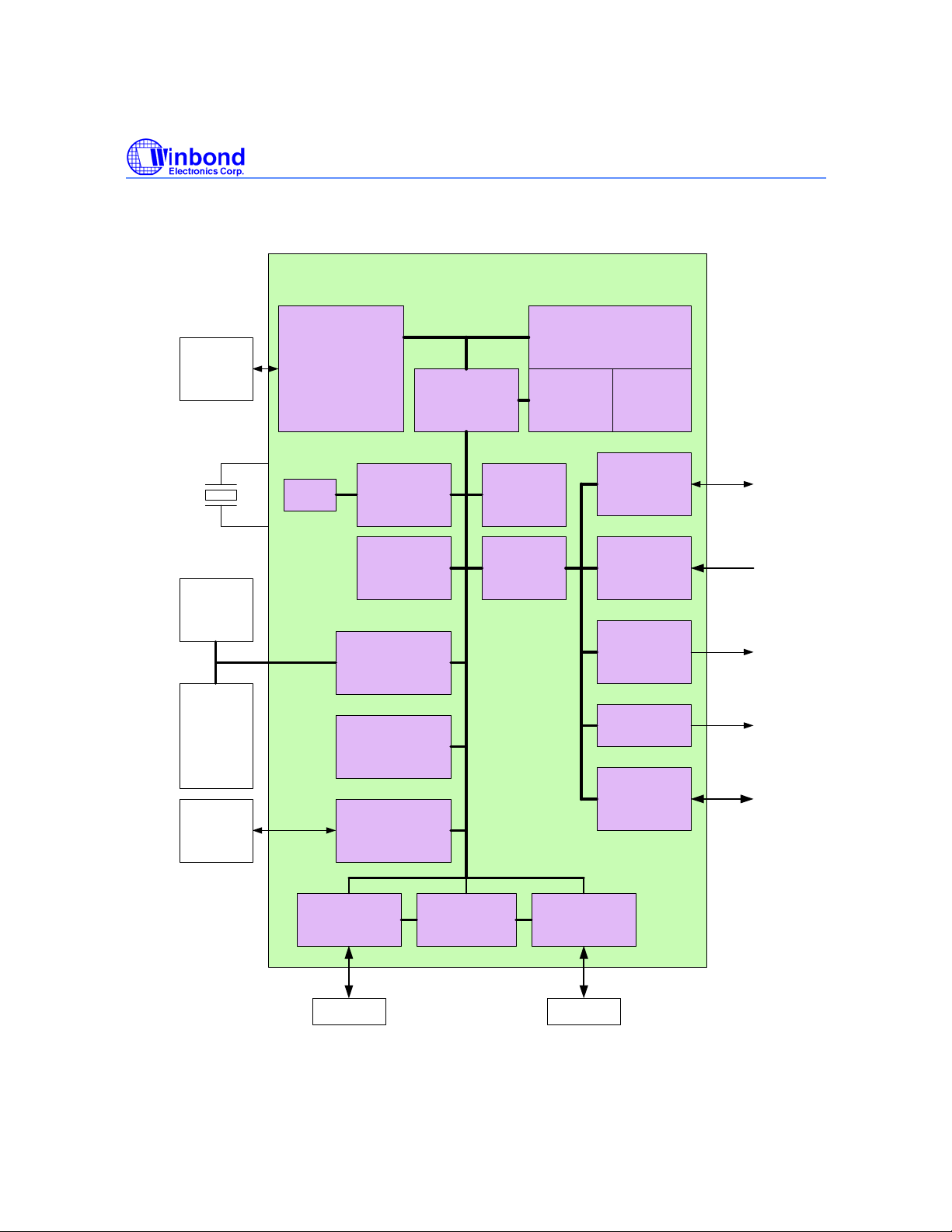
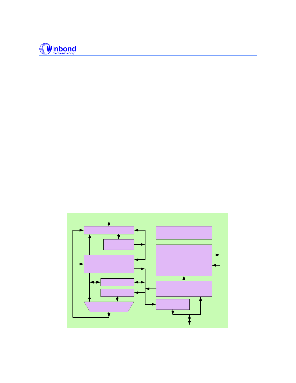
3. BLOCK DIAGRAM
W90N740
W90N740
JTAG
ICE
SDRAM
ROM
Flash
RAM
PCMCIA
IO Dev
ARM7TDMI
PLL
EBI Bus
TDMI Bus
Clock
Controller
AHB
Decoder
External Bus
Controller
GDMA
Controller
Wrapper
AHB Bus
8K-Byte
AHB
Arbiter
APB
Bridge
Cache
Controller
I Cache
APB Bus
2K-Byte
D Cache
UART
Interrupt
Controller
TIMER x2
WDT
COM Port
External
Interrupts
USB
Device
USB Host
Controller
Ethenet
MAC
Controller 0
PHY PHY
Fig 3.1 W90N740 Functional Block Diagram
NAT
Accelerator
- 5 - Revision A4
GPIO
Ethenet
MAC
Controller 1
Publication Release Date: November 26, 2004
Page 10
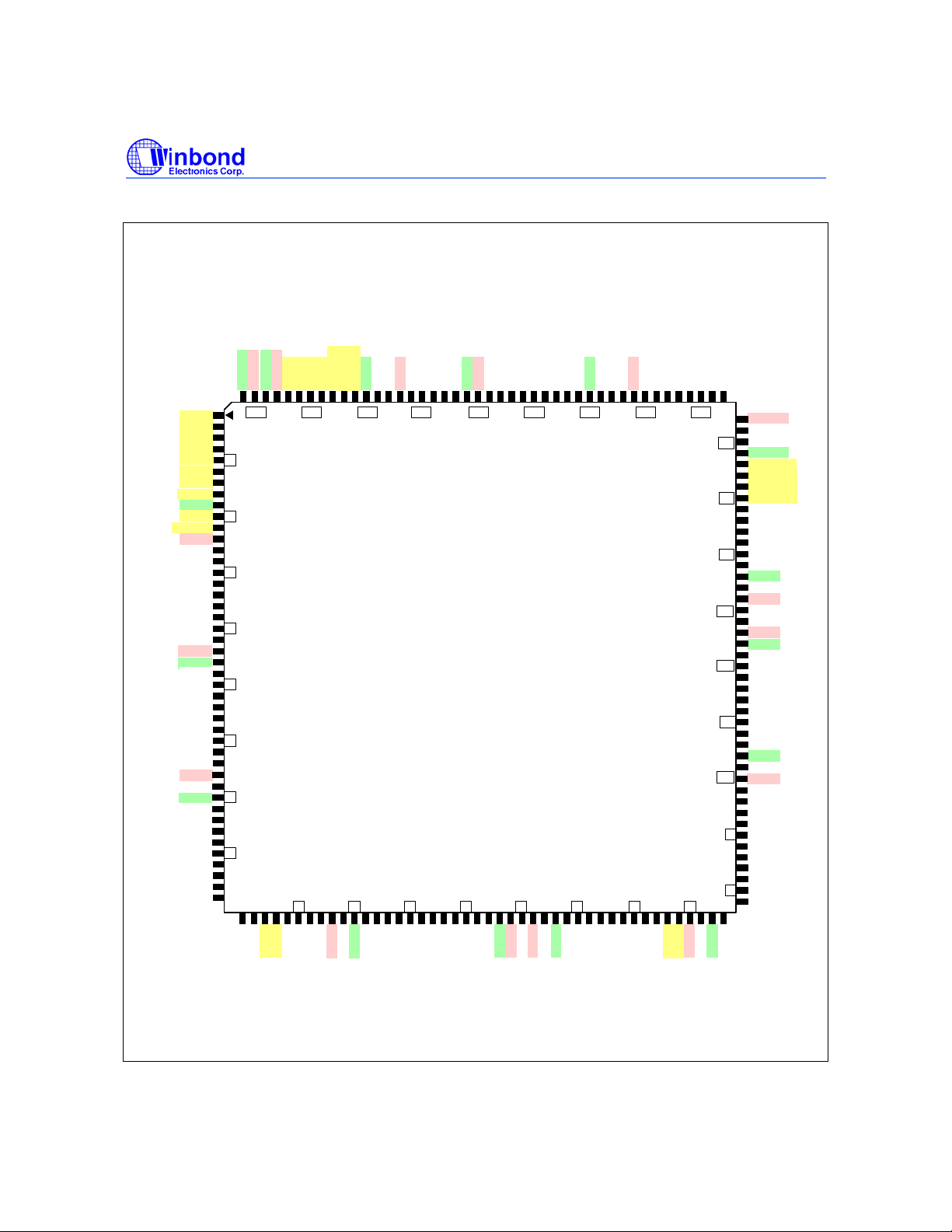
4. PIN CONFIGURATION
RX1_CLK
DVDD18
DVSS18
AVSS18
AVDD18
RX1_DV
RX1D0
RX1D3
RX1D2
RX1D1
RX1_ERR
EXTAL
VSS33
W90N740
GP18/nIRQ1
GP17/nIRQ0
GP20/nIRQ3
GP19/nIRQ2
GP5/nRTS
GP6/nCTS
GP11/RxD
RX0_ERR
RX0_DV
VDD33
XTAL
VDD18
RX0D3
RX0D2
RX0D1
VSS18
TX0_CLK
RX0_CLK
RX0D0
TX0D3
CRS0
COL0
TX0_EN
VSS33
TX0D0
TX0D2
TX0D1
GP10/TxD
VDD33
MDIO0
MDC0
TX1D0
TX1D1
TX1D2
TX1D3
TX1EN
COL1
CRS1
MDIO1
VSS33
MDC1
TX1CLK
VDD33
GP0
GP1
GP2
GP3
GP12/nWDOG
GP13/TIMER0
GP14/TIMER1
TMS
TDI
VDD18
VSS18
TDO
TCK
nTRST
nRESET
P15/nXDACK
P16/nXDREQ
EMACK
EMREQ
nWAIT
VDD33
nOE
VSS33
nECS0
nECS1
nECS2
nECS3
nBTCS
nSCS0
nSCS1
SDQM0
SDQM1
A17
A18
A19
140
A21
A20
135
85
VDD33
A24
A23
A22
D0
USBVDD
DP
DN
130
USBVSS
GP9/nDSR
GP8/nDTR
GP7/nCD
125
GP4/nRI
D31
D30
D29
D28
120
D27
D26
VSS33
D25
VDD33
D24
115
D23
VDD18
VSS18
D22
110
D21
D20
D19
D18
D17
105
D16
D15
D14
VSS33
D13
100
VDD33
D12
D11
D10
D9
95
D8
D7
D6
D5
D4
90
D3
D2
VSS33
D1
165 160 155 150 145175 170
5
10
15
W90N740
20
25
176-Pin LQFP
30
35
40
50 55 60 80757065
SDQM3
SDQM2
NC
NC
MCKE
nSWE
nSCAS
nSRAS
VDD33
VSS33
MCLK
A0A2A1
A3
A8
A7
A6
A5
A4
VDD18
VDD33
A12
A13
VSS33
A16
A15
A14
VSS18
A11
A10
A9
Fig 4.1 176-Pin LQFP Pin Diagram
- 6 -
Page 11
5. PIN ASSIGNMENT
Table 4 W90N740 Pins Assignment
PIN NAME 176-PIN LQFP
Clock & Reset ( 4 pins )
W90N740
EXTAL
XTAL
MCLK
nRESET
TAP Interface ( 5 pins )
TCK
TMS
TDI
TDO
nTRST
External Bus Interface ( 78 pins )
A [24:22]
A [21:0]
D [31:16]
D [15:0]
nWBE [3:0]/ SDQM [3:0]
nSCS[1:0]
NSRAS
NSCAS
NSWE
MCKE
NC
NC
EMREQ
EMACK
nWAIT
NBTCS
nECS[3:0]
NOE
z
164
z
163
z
54
z
27
z
25
z
20
z
21
z
24
z
26
z
84-82
81-74, 72, 70,
z
67-56
124-119, 117,
z
115-114, 111-105
104-103, 101,
z
99-88, 86
z
46-43
z
42, 41
z
51
z
52
z
50
z
49
z
48
z
47
z
31
z
30
z
32
z
40
z
39-36
z
34
Publication Release Date: November 26, 2004
- 7 - Revision A4
Page 12
Table 4 W90N740 Pins Assignment (Continued)
PIN NAME 176-PIN LQFP
Ethernet Interface (0) ( 17 pins )
W90N740
MDC0
MDIO0
COL0 /
CRS0 /
R1B_CRSDV
TX0_CLK
TX0D [3:0] / R1B_TXD [1:0],
R0_TXD [1:0]
TX0_EN / R0_TXEN
RX0_CLK / R0_REFCLK
RX0D [3:0] / R1B_RXD [1:0],
R0_RXD [1:0]
RX0_DV / R0_CRSDV
RX0_ERR
Ethernet Interface (1) ( 17 pins )
MDC1
MDIO1
COL1
CRS1
TX1_CLK
TX1D [3:0] / R1A_TX [1:0]
TX1_EN /R1A_TXEN
RX1_CLK / R1A_REFCLK
RX1D [3:0] / R1A_RXD [1:0]
RX1_DV / R1A_CRSDV
RX1_ERR / R1A_RXERR
z
z
z
z
z
z
z
z
z
z
z
z
z
z
z
z
z
z
z
z
z
z
142
143
151
152
150
149-146
144
153
159-157, 154
160
161
10
8
6
7
11
4-1
5
167
172-169
168
166
- 8 -
Page 13
Table 4 W90N740 Pins Assignment (Continued)
NAME 176-PIN LQFP
USB Interface ( 2 pins )
DP
DN
Miscellaneous ( 21 pins )
GP [20:17] / nIRQ [3:0]
GP16 / nXDREQ
GP15 /nXDACK
GP14 /
TIMER1/ SPEED
GP13 /
TIMER0/ STDBY
GP12 /nWDOG
GP11 /RxD
GP10 /TxD
GP9/nDSR/nTOE
GP8 /nDTR/FSE0
GP7 /nCD / VO
GP6 /nCTS/ VM
GP5 /nRTS/ VP
GP4 /nRI / RCV
GP [3:0]
z
z
z
z
z
z
z
z
z
z
z
z
z
z
z
z
z
W90N740
131
130
136-133
29
28
19
18
17
140
139
128
127
126
138
137
125
16-13
Name 176-Pin LQFP
Power/Ground (32 pins)
VDD18
VSS18
VDD33
VSS33
USBVDD
USBVSS
DVDD18
DVSS18
AVDD18
AVSS18
z
22, 69, 113, 155
z
23, 68, 112, 156
12, 33, 53, 71, 85,
z
100, 116, 141, 162
9, 35, 55, 73, 87, 102, 118, 145,
z
165
z
132
z
129
z
175
z
176
z
173
z
174
Publication Release Date: November 26, 2004
- 9 - Revision A4
Page 14

6. PIN DESCRIPTION
Table 6.1 W90N740 Pins Description
W90N740
PIN NAME
System Clock & Reset
EXTAL I - External Clock / Crystal Input
XTAL O - Crystal Output
MCLK O - System Master Clock Out, SDRAM clock
nRESET I - System Reset, active-low
TAP Interface
TCK ID
TMS IU
TDI IU
TDO O - JTAG Test Data out
nTRST IU
External Bus Interface
A [24:22] O - Address Bus (MSB) of external memory and IO devices
A [21:0] IO - Address Bus of external memory and IO devices
D [31:16] IO - Data Bus (MSB) of external memory and IO device,
D [15:0] IO - Data Bus (LSB) of external memory and IO device
nWBE [3:0]/
SDQM [3:0]
nSCS [1:0] O - SDRAM chip select for two external banks, active-low.
nSRAS O - Row Address Strobe for SDRAM, active-low
nSCAS O - Column Address Strobe for SDRAM, active-low
nSWE O - SDRAM Write Enable, active-low
MCKE O - SDRAM Clock Enable, active-high
EMREQ ID
EMACK O - External Bus Acknowledge
nWAIT IU
nBTCS O - ROM/Flash Chip Select, active-low
nECS [3:0] IO - External I/O Chip Select, active-low.
nOE O - ROM/Flash, External Memory Output Enable, active-low
IO
TYPE
IO -
PAD
TYPE
internal
pulldown
internal
pull-up
internal
pull-up
internal
pull-up
internal
pulldown
internal
pull-up
DESCRIPTION
JTAG Test Clock,
JTAG Test Mode Select,
JTAG Test Data in,
JTAG Reset, active-low,
Write Byte Enable for specific device(nECS[3:0]),
Data input/output Mask signal for SDRAM (nSCS[1:0]), active-low These pins
are always Output in normal mode, and Input type in internal SRAM test mode.
External Master Bus Request
This is used to request external bus. When EMACK active, indicates the bus
grants the bus, chip drives all the output pins of the external bus to high
impedance.
External Wait, active-low
- 10 -
Page 15

Pins Description, continued
W90N740
PIN NAME
Ethernet Interface (0)
MDC0 O
MDIO0 IO
COL0 I
CRS0 I
TX0_CLK I
TX0D [3:0]/
--, R0_TXD
[1:0]
TX0_EN /
R0_TXEN
RX0_CLK /
R0_REFCLK
RX0D [3:0] /
--, R0_RXD
[1:0]
RX0_DV /
R0_CRSDV
RX0_ERR I
IO
TYPE
O
O
I
I
I
PAD
TYPE
-
-
-
-
-
-
-
-
-
-
-
DESCRIPTION
MII Management Data Clock for Ethernet 0. It is the reference clock of MDIO0.
Each MDIO0 data will be latched at the rising edge of MDC0 clock.
MII Management Data I/O for Ethernet 0. It is used to transfer MII control and
status information between PHY and MAC.
Collision Detect for Ethernet 0 in MII mode. This shall be asserted by PHY upon
detecting a collision happened over the medium. It will be asserted and lasted until
collision condition vanishes.
Carrier Sense for Ethernet 0 in MII mode. In RMII mode, external pull-up is
necessary.
Transmit Data Clock for Ethernet 0 in MII mode.
provides the timing reference for TX0_EN and TX0D. The clock will be 25MHz or
2.5 MHz.
Transmit Data bus (4-bit) for Ethernet 0 in MII mode. The nibble transmit data bus
is synchronized with TX0_CLK. It should be latched by PHY at the rising edge of
TX0_CLK.
In RMII mode, TX0D [1:0] are used as R0_TXD [1:0], 2-bit Transmit Data bus for
Ethernet 0;
Transmit Enable for Ethernet 0 in MII. It indicates the transmit activity to external
PHY. It will be synchronized with TX0_CLK.
In RMII mode, R0_TXEN shall be asserted synchronously with the first nibble of
the preamble and shall remain asserted while all di-bits to be transmitted are
presented. Of course, it is synchronized with R0_REFCLK.
Receive Data Clock for Ethernet 0 in MII mode When it is used as a received clock
pin, it is from PHY. The clock will be either 25 MHz or 2.5 MHz. The minimum duty
cycle at its high or low state should be 35% of the nominal period for all conditions.
In RMII mode, this pin is used as R0_REFCLK, Reference Clock;
be 50MHz +/- 50 ppm with minimum 35% duty cycle at high or low state.
Receive Data bus (4-bit) for Ethernet 0 in MII mode. They are driven by external
PHY, and should be synchronized with RX0_CLK and valid only when RX0_DV is
valid.
In RMII mode, RX0D [1:0] are used as R0_RXD [1:0], 2-bit Receive Data bus for
Ethernet 0;
Receive Data Valid for Ethernet 0 in MII mode. It will be asserted when received data
is coming and present, and de-asserted at the end of the frame.
In RMII mode, this pin is used as the R0_CRSDV, Carrier Sense / Receive Data
Valid for Ethernet 0. The R0_CRSDV shall be asserted by PHY when the receive
medium is non-idle. Loss of carrier shall result in the de-assertion of R0_CRSDV
synchronous to the cycle of R0_REFCLK, and only on nibble boundaries.
Receive Data Error for Ethernet 0 in MII mode. It indicates a data error detected by
PHY. The assertion should be lasted for longer than a period of RX0_CLK. When
RX0_ERR is asserted, the MAC will report a CRC error.
TX0_CLK is driven by PHY and
The clock shall
Publication Release Date: November 26, 2004
- 11 - Revision A4
Page 16
Pins Description, continued
W90N740
PIN NAME
Ethernet Interface (1)
MDC1 O -
MDIO1 IO -
COL1 I -
CRS1 I -
TX1_CLK I -
TX1D [3:0] /
--,R1A_TXD [1:0]
TX1_EN/
R1A_TXEN/R1B_TXEN
RX1_CLK /
R1A_REFCLK
RX1D [3:0] /
--, R1A_RXD[1:0]
RX1_DV/
R1A_CRSDV
RX1_ERR /
R1A_RXERR
IO
TYPE
PAD
TYPE
MII Management Data Clock for Ethernet 1. It is the reference clock of MDIO1.
Each MDIO1 data will be latched at the rising edge of MDC1 clock.
MII Management Data I/O for Ethernet 1. It is used to transfer MII control and
status information between PHY and MAC.
Collision Detect for Ethernet 1 in MII mode. This shall be asserted by PHY upon
detecting a collision happened over the medium. It will be asserted and lasted
until collision condition vanishes. External pull-up is necessary in RMII mode.
Carrier Sense for Ethernet 1 in MII mode. External pull-up is necessary in RMII
mode.
Transmit Data Clock for Ethernet 1 in MII mode, TX1_CLK is driven by PHY and
provides the timing reference for TX1_EN and TX1D. The clock will be 25MHz or
2.5 MHz. External pull-up will be necessary in RMII mode.
Transmit Data bus (4-bit) for Ethernet 1 in MII mode. The nibble transmit data
bus is synchronized with TX1_CLK. It should be latched by PHY at the rising
O -
O -
I -
I -
I -
I -
edge of TX1_CLK.
In RMII mode, TX1D [1:0] are used as R1A_TXD [1:0], 2-bit Transmit Data bus
for Ethernet 1
Transmit Enable for Ethernet 1 in MII and RMII mode. It indicates the transmit
activity to external PHY. It will be synchronized with TX1_CLK in MII mode.
Receive Data Clock for Ethernet 1 in MII mode. When it is used as a received
clock pin, it is from PHY. The clock will be either 25 MHz or 2.5 MHz. The
minimum duty cycle at its high or low state should be 35% of the nominal period
for all conditions.
In RMII mode, this pin is used as R1A_REFCLK, Reference Clock and only
available for 176-pin package. The clock shall be 50MHz +/-50 ppm with
minimum 35% duty cycle at high or low state.
Receive Data bus (4-bit) for Ethernet 1 in MII mode. They are driven by external
PHY, and should be synchronized with RX1_CLK and valid only when RX1_DV
is valid.
In RMII mode, RX1D [1:0] are used as R1A_RXD [1:0], 2-bit Receive Data bus
for Ethernet 1.
Receive Data Valid for Ethernet 1 in MII mode. It will be asserted when received
data is coming and present, and de-asserted at the end of the frame.
In RMII mode, this pin is used as the R1A_CRSDV, Carrier Sense / Receive
Data Valid for Ethernet 1 and only available for 176-pin package. The
R1A_CRSDV shall be asserted by PHY when the receive medium is non-idle.
Loss of carrier shall result in the de-assertion of R1A_CRSDV synchronous to
the cycle of R1A_REFCLK, and only on nibble boundaries.
Receive Data Error for Ethernet 1 in MII and RMII mode. It indicates a data error
detected by PHY. The assertion should be lasted for longer than a period of
RX0_CLK. When RX0_ERR is asserted, the MAC will report a CRC error.
DESCRIPTION
- 12 -
Page 17
Pins Description, continued
W90N740
NAME
USB Interface
DP IO - Differential Positive USB IO signal
DN IO - Differential Negative (Minus) USB IO signal
Miscellaneous
GP[20:17] /
nIRQ[3:0]
GP16 / nXDREQ IO
GP15 /nXDACK IO
GP14 /
TIMER1/SPEED
GP13 /
TIMER0/STDBY
GP12 /nWDOG IO
GP11 /RxD IO
GP10 /TxD IO
GP9/nDSR/nTOE IO
GP8 /nDTR/FSE0 IO
GP7 /nCD /VO IO
GP6 /nCTS/ VM IO
GP5 /nRTS/ VP IO
GP4 /nRI /RCV IO
GP[3:0] IO - General Purpose I/O.
IO
TYPE
IO
IO
IO
PAD
TYPE
-
-
-
-
-
-
-
-
-
-
-
-
-
-
DESCRIPTION
External Interrupt Request or General Purpose I/O
External DMA Request or General Purpose I/O
External DMA Acknowledge or General Purpose I/O
Timer 1 or General Purpose I/O. This pin is also used as SPEED,
Speed mode control for external USB transceiver
Timer 0 or General Purpose I/O. This pin is also used as STDBY, StandBy control
for external USB transceiver
Watchdog Timer Timeout Flag (active-low) or General Purpose I/O
UART Receive Data or General Purpose I/O
UART Transmit Data or General Purpose I/O
UART Receive Clock or General Purpose I/O. This pin is also used as nTOE,
Output Enable control (active-low) for external USB transceiver.
UART Transmit Clock or General Purpose I/O. This pin is also used as SE0,
Differential Data Transceiver Output for external USB transceiver. T
UART Carrier Detector or General Purpose I/O. This pin is also used as VO, Data
Output for external USB transceiver.
UART Clear to Send or General Purpose I/O. This pin is also used as VM, Data
Negative (Minus) Input for external USB receiver.
UART Ready to Send or General Purpose I/O. This pin is also used as VP, Data
Positive Input for external USB receiver.
UART Ring Indicator or General Purpose I/O. This pin is also used as RCV,
Difference Receiver Input.
Power/Ground
VDD18 P Core Logic power (1.8V)
VSS18 G Core Logic ground (0V)
VDD33 P IO Buffer power (3.3V)
VSS33 G IO Buffer ground (0V)
USBVDD P USB power (3.3V)
USBVSS G USB ground (0V)
DVDD18 P PLL Digital power (1.8V)
DVSS18 G PLL Digital ground (0V)
AVDD18 P PLL Analog power (1.8V)
AVSS18 G PLL Analog ground (0V)
Publication Release Date: November 26, 2004
- 13 - Revision A4
Page 18
W90N740
7. FUNCTIONAL DESCRIPTION
7.1 ARM7TDMI CPU Core
The ARM7TDMI CPU core is a member of the ARM family of general-purpose 32-bit microprocessors,
which offer high performance for very low power consumption. The architecture is based on Reduced
Instruction Set Computer (RISC) principles, and the instruction set and related decode mechanism are
much simpler than those of micro-programmed Complex Instruction Set Computer (CISC) systems.
Pipelining is employed so that all parts of the processing and memory systems can operate continuously.
The high instruction throughput and impressive real-time interrupt response are the major benefits.
The ARM7TDMI core can execute two instruction sets:
(1) The standard 32-bit ARM instruction set
(2) The 16-bit THUMB instruction set
The THUMB set’s 16-bit instruction length allows it to approach twice the density of standard ARM core
while retaining most of the ARM’s performance advantage over a traditional 16-bit processor using 16-bit
registers. THUMB instructions operate with the standard ARM register configuration, allowing excellent
interoperability between ARM and THUMB states. Each 16-bit THUMB instruction has a corresponding
32-bit ARM instruction with the same effect on the processor model. In the other words, the THUMB
architecture give 16-bit systems a way to access the 32-bit performance of the ARM Core without
requiring the full overhead of 32-bit processing.
ARM7TDMI CPU core has 31 x 32-bit registers. At any one time, 16 set are visible; the other registers
are used to speed up exception processing. All the register specifies in ARM instructions can address
any of the 16 registers. The CPU also supports 5 types of exception, such as two levels of interrupt,
memory aborts, attempted execution of an undefined instruction and software interrupts.
A[31:0]
ALU Bus
Address Register
PC Bus
(31 x 32-bit registers)
(6 status registers)
A Bus
Address
Incrementer
Register Bank
32 x8 Multiplier
Barrel Shifter
32-bit ALU
Incrementer Bus
B Bus
Scan Control
Instruction Decoder
Control Logic
Instruction Pipeline
Read Data Register
Thumb Instruction Decoder
Writer Data
Register
D[31:0]
Fig 7.1 ARM7TDMI CPU Core Block Diagram
- 14 -
Page 19

W90N740
7.2 System Manager
7.2.1 Overview
The functions of the System Manager:
• System memory map & on-chip peripherals memory map
• The data bus width of external memory address & data bus connection with external memory
• Bus arbitration supports the Fixed Priority Mode & Rotate Priority Mode
• Power-On setting
• On-Chip PLL module control & Clock select control
7.2.2 System Memory Map
W90N740 provides 2G bytes cacheable address space and the other 2G bytes are non-cacheable. The
On-Chip Peripherals bank is on 1M bytes top of the space (0xFFF0.0000 – 0xFFFF.FFFF) and the OnChip RAM bank’s start address is 0xFFE0.0000, the other banks can be located anywhere (cacheable
space: 0x0~0x7FDF.FFFF if Cache ON; non-cacheable space: 0x8000.0000 ~ 0xFFDF.FFFF).
The size and location of each bank is determined by the register settings for “current bank base address
pointer” and “current bank size”. (*Note: The address boundaries of consecutive banks must not overlap,
when setting the bank control registers.)
The start address of each memory bank is not fixed, except On-Chip Peripherals and On-Chip RAM. You
can use bank control registers to assign a specific bank start address by setting the bank’s base pointer
(13 bits). The address resolution is 256K bytes. The bank’s start address is defined as “base pointer <<
18” and the bank’s size is “current bank size”.
In the event of an access request to an address outside any programmed bank size, an abort signal is
generated. The maximum accessible memory size of each external IO bank is 32M bytes, and 64M
bytes on SDRAM banks.
Publication Release Date: November 26, 2004
- 15 - Revision A4
Page 20
0x7FFF.FFFF
512KB
(Fixed)
0x7FF8.0000
512KB
(Fixed)
0x7FF0.0000
W90N740
Cacheable space Non-Cacheable space
RESERVED
RESERVED
RESERVED
0xFFFF.FFFF
512KB
(Fixed)
0xFFF8.0000
512KB
(Fixed)
0xFFF0.0000
On-Chip APB
Peripherals
On-Chip AHB
Peripherals
RESERVED
10KB
0x7FE0.0000
EBI Space
RESERVED
External I/O Bank 3
256KB - 32MB
External I/O Bank 2
256KB - 32MB
External I/O Bank 1
256KB - 32MB
External I/O Bank 0
256KB - 32MB
SDRAM Bank 1
2MB - 64MB
SDRAM Bank 0
2MB - 64MB
10KB
0xFFE0.0000
EBI Space
On-Chip RAM
2KB,8KB
External I/O Bank 3
256KB - 32MB
External I/O Bank 2
256KB - 32MB
External I/O Bank 1
256KB - 32MB
External I/O Bank 0
256KB - 32MB
SDRAM Bank 1
2MB - 64MB
SDRAM Bank 0
2MB - 64MB
0x0000.0000
ROM/FLASH
256KB - 32MB
Fig7.2.1 System Memory Map
ROM/FLASH
256KB - 32MB
0x8000.0000
- 16 -
Page 21
Table 7.2.1 On-Chip Peripherals Memory Map
BASE ADDRESS DESCRIPTION
AHB Peripherals
0xFFF0.0000 Product Identifier Register (PDID)
0xFFF0.0004
0xFFF0.0008
0xFFF0.000C
0xFFF0.1000
0xFFF0.1004
0xFFF0.1008
0xFFF0.1018
0xFFF0.2000
0xFFF0.3000
0xFFF0.4000
0xFFF0.5000
0xFFF0.6000
0xFFF6.0000
0xFFF7.0000
Arbitration Control Register (ARBCON)
PLL Control Register (PLLCON)
Clock Select Register (CLKSEL)
EBI Control Register (EBICON)
ROM/FLASH (ROMCON)
SDRAM bank 0 - 1
External I/O 0 - 3
Cache Controller
Ethernet MAC Controller 0 - 1
GDMA 0 - 1
USB (Host)
NAT Accelerator
Reserved
Reserved
APB Peripherals
W90N740
0xFFF8.0000
0xFFF8.1000
0xFFF8.2000
0xFFF8.3000
UART
Timer 0 - 1, WDOG Timer
Interrupt Controller
GPIO
7.2.3 Address Bus Generation
The W90N740 address bus generation is depended on the required data bus width of each memory
bank. The data bus width is determined by DBWD bits in each bank’s control register.
The maximum accessible memory size of each external IO bank is 32M bytes .
Table 7.2.2 Address Bus Generation Guidelines
DATA BUS EXTERNAL ADDRESS PINS MAXIMUM ACCESSIBLE
Width A [22:0] A23 A24 Memory Size
8-bit A22 – A0 (Internal) A23 (Internal) A24 (Internal) 32M bytes
16-bit A23 – A1 (Internal) A24 (Internal) NA 16M half-words
32-bit A24 – A2 (Internal) NA NA 8M words
Publication Release Date: November 26, 2004
- 17 - Revision A4
Page 22
W90N740
7.2.4 Data Bus Connection with External Memory
7.2.4.1 Memory formats
The internal architecture is big endian. The little endian mode only support for external memory.
The W90N740 can be configured as big endian or little endian mode by pull up or down the data D14
pin. If D14 is pull-up then it is a little endian mode, otherwise, it is a big endian mode.
Big Endian
In Big endian format, the W90N740 stores the most significant byte of a word at the lowest numbered
byte, and the least significant byte at the highest-numbered byte. So the byte at address 0 of the memory
system connects to data lines 31 through 24.
For a word aligned address A, Fig7.2.2 shows how the word at address A, the half-word at addresses A
and A+2, and the bytes at addresses A, A+1, A+2, and A+3 map on to each other when the LITTLE pin
is Low.
31 30 29 28 27 26 25 24 23 22 21 20 19 18 17 16 15 14 13 12 11 10 9 8 7 6 5 4 3 2 1 0
Word at address A
Half-word at address A Half-word at address A+2
Byte at address A Byte at address A+1 Byte at address A+2 Byte at address A+3
Fig. 7.2.2 Big endian addresses of bytes and half-words within words
Little Endian
In Little endian format, the lowest addressed byte in a word is considered the least significant byte of the
word and the highest addressed bye is the most significant. So the byte at address 0 of the memory
system connects to data lines 7 through 0.
For a word aligned address A, Fig7.2.3 shows how the word at address A, the half-word at addresses A
and A+2, and the bytes at addresses A, A+1, A+2, and A+3 map on to each other when LITTLE pin is
High.
31 30 29 28 27 26 25 24 23 22 21 20 19 18 17 16 15 14 13 12 11 10 9 8 7 6 5 4 3 2 1 0
Word at address A
Half-word at address A+2 Half-word at address A
Byte at address A+3 Byte at address A+2 Byte at address A+1 Byte at address A
Fig. 7.2.3 Little endian addresses of bytes and half-words within words
- 18 -
Page 23
W90N740
7.2.4.2 Connection of External Memory with Various Data Width
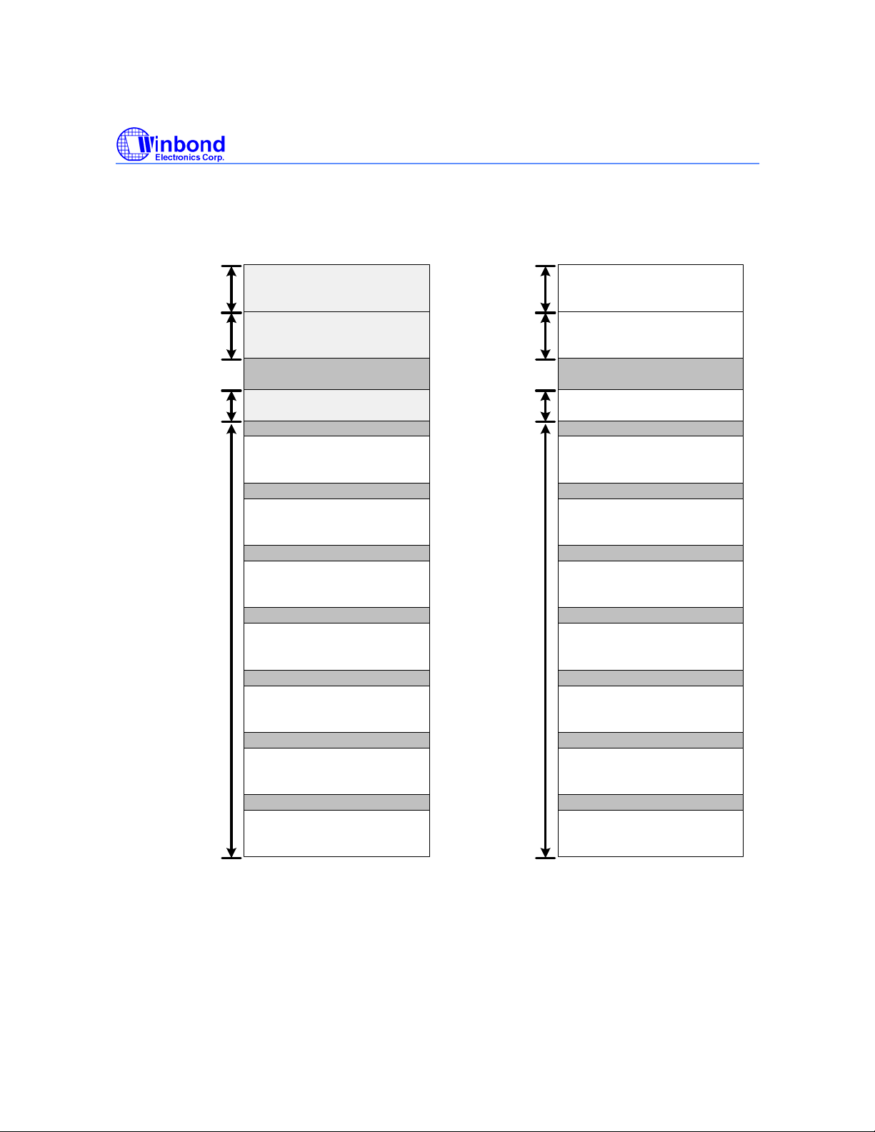
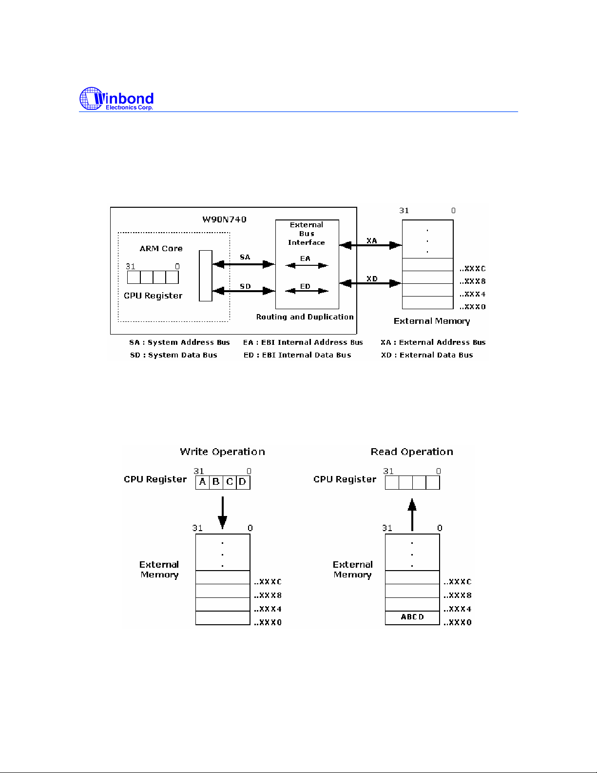
The system diagram for W90N740 connecting with the external memory is shown in Fig. 7.2.4. Below
tables (Table7.2.3 − Table7.2.14) show the program/data path between CPU register and the external
memory using little / big endian and word/half-word/byte access.
Fig. 7.2.4 Address/Data bus connection with external memory
Fig. 7.2.5 CPU register Read/Write with external memory
Publication Release Date: November 26, 2004
- 19 - Revision A4
Page 24

W90N740
Table 7.2.3 and Table 7.2.4
Using big-endian and word access, Program/Data path between register and external memory
WA = Address whose LSB is 0, 4, 8, C X = Don’t care
nWBE [3-0] / SDQM [3-0] = A means active and U means inactive
Table7.2.3 Word access write operation with Big Endian
Access Operation Write Operation (CPU Register Î External Memory)
XD Width Word Half Word Byte
Bit Number
CPU Reg Data
SA
Bit Number
SD
Bit Number
ED
XA
nWBE [3-0] /
SDQM [3-0]
Bit Number
XD
Bit Number
Ext. Mem Data
Timing Sequence
31 0
ABCD
WA WA WA
31 0
ABCD
31 0
ABCD
WA WA WA+2 WA WA+1 WA+2 WA+3
AAAA XXAA XXAA XXXA XXXA XXXA XXXA
31 0
ABCD
31 0
ABCD
1st write 2nd write 1st write 2nd write 3rd write 4th write
15 0
AB
15 0
AB
15 0
AB
31 0
ABCD
31 0
AB CD
15 0
CD
15 0
CD
15 0
CD
7 0
A
7 0
A
7 0
A
7 0
B
7 0
B
7 0
B
31 0
ABCD
31 0
A B C D
7 0
C
7 0
C
7 0
C
7 0
D
7 0
D
7 0
D
Table7.2.4 Word access read operation with Big Endian
Access Operation Read Operation (CPU Register Í External Memory)
XD Width Word Half Word Byte
Bit Number
CPU Reg Data
SA
Bit Number
SD
Bit Number
ED
XA
SDQM [3-0]
Bit Number
XD
Bit Number
Ext. Mem Data
Timing Sequence
31 0
ABCD
WA WA WA
31 0
ABCD
31 0
ABCD
WA WA WA+2 WA WA+1 WA+2 WA+3
AAAA XXAA XXAA XXXA XXXA XXXA XXXA
31 0
ABCD
31 0
ABCD
1st read 2nd read 1st read 2nd read 3rd read 4th read
31 0
CD XX
15 0
CD
15 0
CD
31 0
CDAB
31 0
CD AB
31 0
CD AB
15 0
AB
15 0
AB
31 0
D X X X
7 0
D
7 0
D
31 0
DCBA
31 0
D C B A
31 0
D C X X
7 0
C
7 0
C
- 20 -
31 0
D C B X
7 0
B
7 0
B
31 0
D C B A
7 0
A
7 0
A
Page 25
W90N740
Table 7.2.5 and Table 7.2.6
Using big-endian and half-word access, Program/Data path between register and external memory.
HA = Address whose LSB is 0, 2, 4, 6, 8, A, C, E HAL = Address whose LSB is 0, 4, 8, C
HAU = Address whose LSB is 2, 6, A, E X = Don’t care
nWBE [3-0] / SDQM [3-0] = A means active and U means inactive
Table7.2.5 Half-word access write operation with Big Endian
Access Operation Write Operation (CPU Register Î External Memory)
XD Width Word Half Word Byte
Bit Number
CPU Reg Data
SA
Bit Number
SD
Bit Number
ED
XA
nWBE [3-0] /
SDQM [3-0]
Bit Number
XD
Bit Number
Ext. Mem Data
Timing Sequence 1st write 2nd write
31 0
ABCD
HAL HAU HA HA
31 0
CD CD
31 0
CD CD
HAL HAL HA HA HA+1
AAUU UUAA XXAA XXXA XXXA
31 0
CD CD
31 16
CD
31 0
CD CD
31 0
CD CD
31 0
CD CD
15 0
CD
31 0
ABCD
31 0
CD CD
31 0
CD CD
15 0
CD
15 0
CD
31 0
CD CD
7 0
C
7 0
C
7 0
C
31 0
ABCD
31 0
CD CD
7 0
D
7 0
D
7 0
D
Table7.2.6 Half-word access read operation with Big Endian
Access Operation Read Operation (CPU Register Í External Memory)
XD Width Word Half Word Byte
Bit Number
CPU Reg Data
SA
Bit Number
SD
Bit Number
ED
XA
SDQM [3-0]
Bit Number
XD
Bit Number
Ext. Mem Data
Timing Sequence 1st read 2nd read
15 0
AB
HAL HAU HA HA
15 0
AB
15 0
AB
HAL HAL HA HA HA+1
AAUU UUAA XXAA XXXA XXXA
31 0
AB CD
31 0
ABCD
15 0
CD
15 0
CD
15 0
CD
31 0
AB CD
15 0
CD
15 0
CD
15 0
CD
15 0
CD
15 0
CD
15 0
DX
7 0
D
7 0
D
15 0
DC
15 0
DC
15 0
DC
7 0
C
7 0
C
Publication Release Date: November 26, 2004
- 21 - Revision A4
Page 26

W90N740
Table 7.2.7 and Table 7.2.8
Using big-endian and byte access, Program/Data path between register and external memory.
BA = Address whose LSB is 0, 1, 2, 3, 4, 5, 6, 7, 8, 9, A, B, C, D, E, F
BAL = Address whose LSB is 0, 2, 4, 6, 8, A, C, E BAU = Address whose LSB is 1, 3, 5, 7, 9, B, D,
F
BA0 = Address whose LSB is 0, 4, 8, C BA1 = Address whose LSB is 1, 5, 9, D
BA2 = Address whose LSB is 2, 6, A, E BA3 = Address whose LSB is 3, 7, B, F
Table7.2.7 Byte access write operation with Big Endian
Access Operation Write Operation (CPU Register Î External Memory)
XD Width Word Half Word Byte
Bit Number
CPU Reg Data
SA
Bit Number
SD
Bit Number
ED
XA
nWBE [3-0] /
SDQM [3-0]
Bit Number
XD
Bit Number
Ext. Mem Data
Timing Sequence
31 0
ABCD
BA0 BA1 BA2 BA3 BAL BAU BA
31 0
D D D D
31 24
D
BA0 BA0 BA0 BA0 BAL BAL BA
AUUU UAUU UUAU UUUA XXAU XXUA XXXA
31 0
D X X X
31 24
D
31 0
D D D D
23 16
D
31 0
X D X X
23 16
D
31 0
D D D D
15 8
31 0
X X D X
15 8
31 0
D D D D
7 0
D
D
D
31 0
X X X D
7 0
D
31 0
D D D D
15 8
D
15 0
D X
15 8
D
31 0
ABCD
31 0
D D D D
7 0
D
15 0
X D
7 0
D
31 0
ABCD
31 0
D D D D
7 0
D
7 0
D
7 0
D
- 22 -
Page 27

W90N740
Table7.2.8 Byte access read operation with Big Endian
Access Operation Read Operation (CPU Register Í External Memory)
XD Width Word Half Word Byte
Bit Number
CPU Reg Data
SA
Bit Number
SD
Bit Number
ED
XA
SDQM [3-0]
Bit Number
XD
Bit Number
Ext. Mem Data
Timing Sequence
7 0
A
BA0 BA1 BA2 BA3 BAL BAU BA
7 0
A
7 0
A
BA0 BA0 BA0 BA0 BAL BAL BA
AUUU UAUU UUAU UUUA XXAU XXUA XXXA
31 0
ABCD
7 0
B
7 0
B
15 8
B
31 0
ABCD
31 0
ABCD
7 0
C
7 0
C
23 16
C
31 0
ABCD
7 0
D
7 0
D
31 24
D
31 0
ABCD
7 0
C
7 0
C
7 0
C
15 0
CD
7 0
D
7 0
D
15 8
D
15 0
CD
15 0
CD
7 0
D
7 0
D
7 0
D
7 0
D
7 0
D
Publication Release Date: November 26, 2004
- 23 - Revision A4
Page 28

W90N740
Table 7.2.9 and Table 7.2.10
Using little-endian and word access, Program/Data path between register and external memory
WA = Address whose LSB is 0, 4, 8, C X = Don’t care
nWBE [3-0] / SDQM [3-0] = A means active and U means inactive
Table7.2.9 Word access write operation with Little Endian
Access Operation Write Operation (CPU Register Î External Memory)
XD Width Word Half Word Byte
Bit Number
CPU Reg Data
SA
Bit Number
SD
Bit Number
ED
XA
nWBE [3-0] /
SDQM [3-0]
Bit Number
XD
Bit Number
Ext. Mem Data
Timing Sequence
31 0
ABCD
WA WA WA
31 0
ABCD
31 0
ABCD
WA WA WA+2 WA WA+1 WA+2 WA+3
AAAA XXAA XXAA XXXA XXXA XXXA XXXA
31 0
ABCD
31 0
ABCD
1st write 2nd write 1st write 2nd write 3rd write 4th write
15 0
CD
15 0
CD
15 0
CD
31 0
ABCD
31 0
AB CD
15 0
AB
15 0
AB
15 0
AB
7 0
D
7 0
D
7 0
D
7 0
C
7 0
C
7 0
C
31 0
ABCD
31 0
A B C D
7 0
B
7 0
B
7 0
B
7 0
A
7 0
A
7 0
A
Table7.2.10 Word access read operation with Little Endian
Access Operation Read Operation (CPU Register Í External Memory)
XD Width Word Half Word Byte
Bit Number
CPU Reg Data
SA
Bit Number
SD
Bit Number
ED
XA
SDQM [3-0]
Bit Number
XD
Bit Number
Ext. Mem Data
Timing Sequence
31 0
ABCD
WA WA WA
31 0
ABCD
31 0
ABCD
WA WA WA+2 WA WA+1 WA+2 WA+3
AAAA XXAA XXAA XXXA XXXA XXXA XXXA
31 0
ABCD
31 0
ABCD
1st read 2nd read 1st read 2nd read 3rd read 4th read
31 0
XX CD
15 0
CD
15 0
CD
31 0
ABCD
31 0
AB CD
31 0
AB CD
15 0
AB
15 0
AB
31 0
X X X D
7 0
D
7 0
D
A B C D
31 0
X X C D
7 0
C
7 0
C
31 0
ABCD
31 0
31 0
X B C D
- 24 -
7 0
B
7 0
B
31 0
A B C D
7 0
A
7 0
A
Page 29

W90N740
Table 7.2.11 and Table 7.2.12
Using little-endian and half-word access, Program/Data path between register and external memory.
HA = Address whose LSB is 0, 2, 4, 6, 8, A, C, E HAL = Address whose LSB is 0,4,8,C
HAU = Address whose LSB is 2, 6, A, E X = Don’t care
nWBE [3-0] / SDQM [3-0] = A means active and U means inactive
Table7.2.11 Half-word access write operation with Little Endian
Access Operation Write Operation (CPU Register Î External Memory)
XD Width Word Half Word Byte
Bit Number
CPU Reg Data
SA
Bit Number
SD
Bit Number
ED
XA
nWBE [3-0] /
SDQM [3-0]
Bit Number
XD
Bit Number
Ext. Mem Data
Timing Sequence
31 0
ABCD
HAL HAU HA HA
31 0
CD CD
31 0
CD CD
HAL HAL HA HA HA+1
UUAA AAUU XXAA XXXA XXXA
31 0
CD CD
15 0
CD
31 0
CD CD
31 0
CD CD
31 0
CD CD
31 16
CD
31 0
ABCD
31 0
CD CD
31 0
CD CD
15 0
CD
15 0
CD
31 0
CD CD
7 0
D
7 0
D
7 0
D
31 0
ABCD
31 0
CD CD
7 0
C
7 0
C
7 0
C
1st write 2nd write
Table7.2.12 Half-word access read operation with Little Endian
Access Operation Read Operation (CPU Register Í External Memory)
XD Width Word Half Word Byte
Bit Number
CPU Reg Data
SA
Bit Number
SD
Bit Number
ED
XA
SDQM [3-0]
Bit Number
XD
Bit Number
Ext. Mem Data
Timing Sequence
15 0
CD
HAL HAU HA HA
15 0
CD
15 0
CD
HAL HAL HA HA HA+1
UUAA AAUU XXAA XXXA XXXA
31 0
AB CD
31 0
ABCD
15 0
AB
15 0
AB
15 0
AB
31 0
AB CD
15 0
CD
15 0
CD
15 0
CD
15 0
CD
15 0
CD
15 0
XD
7 0
D
7 0
D
15 0
CD
15 0
CD
15 0
CD
7 0
C
7 0
C
1st read 2nd read
Publication Release Date: November 26, 2004
- 25 - Revision A4
Page 30
W90N740
Table 7.2.13 and Table 7.2.14
Using little-endian and byte access, Program/Data path between register and external memory.
BA = Address whose LSB is 0, 1, 2, 3, 4, 5, 6, 7, 8, 9, A, B, C, D, E, F
BAL = Address whose LSB is 0, 2, 4, 6, 8, A, C, E BAU = Address whose LSB is 1, 3, 5, 7, 9, B, D, F
BA0 = Address whose LSB is 0, 4, 8, C BA1 = Address whose LSB is 1, 5, 9, D
BA2 = Address whose LSB is 2, 6, A, E BA3 = Address whose LSB is 3, 7, B, F
Table7.2.13 Byte access write operation with Little Endian
Access Operation Write Operation (CPU Register Î External Memory)
XD Width Word Half Word Byte
Bit Number
CPU Reg Data
SA
Bit Number
SD
Bit Number
ED
XA
nWBE [3-0] /
SDQM [3-0]
Bit Number
XD
Bit Number
Ext. Mem Data
Timing Sequence
BA0 BA1 BA2 BA3 BAL BAU BA
31 0
D D D D
7 0
D
BA0 BA0 BA0 BA0 BAL BAL BA
UUUA UUAU UAUU AUUU XXUA XXAU XXXA
31 0
X X X D
7 0
D
31 0
D D D D
31 0
X X D X
15 8
D
15 8
D
31 0
ABCD
31 0
D D D D
23 16
D
31 0
X D X X
23 16
D
31 0
D D D D
31 24
D
31 0
D X X X
31 24
D
31 0
D D D D
7 0
D
15 0
X D
7 0
D
31 0
ABCD
31 0
D D D D
15 8
D
15 0
D X
15 8
D
31 0
ABCD
31 0
D D D D
7 0
D
7 0
D
7 0
D
Table7.2.14 Byte access read operation with Little Endian
Access Operation Read Operation (CPU Register Í External Memory)
XD Width Word Half Word Byte
Bit Number
CPU Reg Data
SA
Bit Number
SD
Bit Number
ED
XA
SDQM [3-0]
Bit Number
XD
Bit Number
Ext. Mem Data
Timing Sequence
7 0
D
BA0 BA1 BA2 BA3 BAL BAU BA
7 0
D
7 0
D
BA0 BA0 BA0 BA0 BAL BAL BA
UUUA UUAU UAUU AUUU XXUA XXAU XXXA
31 0
ABCD
7 0
C
7 0
C
7 0
C
31 0
ABCD
31 0
ABCD
7 0
B
7 0
B
7 0
B
31 0
ABCD
7 0
A
7 0
A
7 0
A
31 0
ABCD
7 0
D
7 0
D
7 0
D
15 0
CD
7 0
C
7 0
C
7 0
C
15 0
CD
15 0
CD
- 26 -
7 0
D
7 0
D
7 0
D
7 0
D
7 0
D
Page 31

W90N740
7.2.5 Bus Arbitration
The W90N740’s internal function blocks or external devices can request mastership of the system bus
and then hold the system bus in order to perform data transfers. The design of W90N740 bus allows only
one bus master at a time, a bus controller is required to arbitrate when two or more internal units or
external devices simultaneously request bus mastership. When bus mastership is granted to an internal
function block or an external device, other pending requests are not acknowledged until the previous bus
master has released the bus.
W90N740 supports two priority modes, the Fixed Priority Mode and the Rotate Priority Mode,
depends on the PRTMOD bit setting.
7.2.5.1 Fixed Priority Mode
In Fixed Priority Mode (PRTMOD = 0, default value), to facilitate bus arbitration, priorities are assigned
to each internal W90N740 function block. The bus controller arbitration requests for the bus mastership
according to these fixed priorities. In the event of contention, mastership is granted to the function block
with the highest assigned priority. These priorities are listed in Table 7.2.15.
W90N740 allows raising ARM Core priority to second if an unmasked interrupt occurred. If IPEN bit, Bit
22 of the Arbitration Control Register (ARBCON), is set to “0”, the priority of ARM Core is fixed to
lowest. If IPEN bit is set to “1” and if no unmasked interrupt request, then the ARM Core’s priority is still
lowest and the IPACT = 0, Bit 23 of the Arbitration Control Register (ARBCON) ; If there is an
unmasked interrupt request, then the ARM Core’s priority is raised to second and IPACT = 1.
If IPEN is set, an interrupt handler will normally clear IPACT at the end of the interrupt routine to allow an
alternate bus master to regain the bus; however, if IPEN is cleared, no additional action need be taken in
the interrupt handler. The IPACT bit can be read and write. Writing with “0”, the IPACT bit is cleared, but
it will be no effect as writing with “1”.
Table 7.2.15 Bus Priorities for Arbitration in Fixed Priority Mode
Bus Function Block
Priority IPACT = 0 IPEN = 1 and IPACT = 1
1 (Highest) External Bus Master External Bus Master
2 NAT Accelerator ARM Core
3 General DMA0 NAT Accelerator
4 General DMA1 General DMA0
5 EMC0 DMA General DMA1
6 EMC1 DMA EMC0 DMA
7 USB (Host) EMC1 DMA
8 (Lowest) ARM Core USB (Host)
Publication Release Date: November 26, 2004
- 27 - Revision A4
Page 32

W90N740
7.2.5.2 Rotate Priority Mode
In Rotate Priority Mode (PRTMOD = 1), the IPEN and IPACT bits have no function (i.e. ignore).
W90N740 used a round robin arbitration scheme ensures that all bus masters (except the External Bus
Master, it always has the first priority) have equal chance to gain the bus and that a retracted master
does not lock up the bus.
7.2.6 Power-On Setting
After power on reset, there are four Power-On setting pins to configure W90N740 system configuration.
Power-On Setting Pin
Internal System Clock Select D15
Little/Big Endian Mode Select D14
Boot ROM/FLASH Data Bus Width D [13:12]
D15 pin:Internal System Clock Select
If pin D15 is pull-down, the external clock from EXTAL pin is served as internal system clock.
If pin D15 is pull-up, the PLL output clock is used as internal system clock.
D14 pin:Little/Big Endian Mode Select
If pin D14 is pull-down, the external memory format is Big Endian mode.
If pin D14 is pull-up, the external memory format is Little Endian mode.
D [13:12] : Boot ROM/FLASH Data Bus Width
D [13:12] Bus Width
Pull-down Pull-down 8-bit
Pull-down Pull-up 16-bit
Pull-up Pull-down 32-bit
Pull-up Pull-up RESERVED
Note: Related Power-On Setting Pin
D [11:10] :
D [15] D [11:10] Description
Pull-up Pull High W90N740 normal operation
D [9:8] :
D [9:8]
Pull-up Pull-up
- 28 -
Page 33

W90N740
7.2.7 System Manager Control Registers Map
Register Address R/W Description Reset Value
PDID 0xFFF0.0000 R Product Identifier Register 0xX090.0740
ARBCON 0xFFF0.0004 R/W Arbitration Control Register 0x0000.0000
PLLCON 0xFFF0.0008 R/W PLL Control Register 0x0000.2F01
CLKSEL 0xFFF0.000C R/W Clock Select Register 0x0000.3FX8
Product Identifier Register (PDID)
This register is for read only and enables software to recognize certain characteristics of the chip ID and
the version number.
Register Address R/W Description Reset Value
PDID 0xFFF0.0000 R Product Identifier Register 0xX090.0740
31 30 29 28 27 26 25 24
PACKAGE 1
23 22 21 20 19 18 17 16
CHPID
15 14 13 12 11 10 9 8
CHPID
7 6 5 4 3 2 1 0
CHPID
PACKAGE [31:30] Package Type
Package [31:30] Bus Width
1 1 176-pin Package
CHPID [23:0]: Chip identifier
The Chip identifier of W90N740 is 0x90.0740
Publication Release Date: November 26, 2004
- 29 - Revision A4
Page 34

W90N740
Arbitration Control Register (ARBCON)
Register Address R/W Description Reset Value
ARBCON
31 30 29 28 27 26 25 24
23 22 21 20 19 18 17 16
15 14 13 12 11 10 9 8
7 6 5 4 3 2 1 0
IPACT [2] : Interrupt priority active
When IPEN=”1”, this bit is set when the ARM core has an unmasked interrupt request.
This bit is available only when the PRTMOD = 0.
IPEN [1] : Interrupt priority enable bit
0 = the ARM core has the lowest priority.
0xFFF0.0004 R/W
RESERVED IPACT IPEN PRTMOD
Arbitration Control Register
RESERVED
RESERVED
RESERVED
0x0000.0000
1 = enable to raise the ARM core priority to second
This bit is available only when the PRTMOD = 0.
PRTMOD [0] : Priority mode select
0 = Fixed Priority Mode (default)
1 = Rotate Priority Mode
- 30 -
Page 35

W90N740
PLL Control Register (PLLCON)
W90N740 provides two options for clock generation - crystal and oscillator.
The external clock via EXTAL input pin as the reference clock input of PLL module. The external clock
can bypass the PLL and be used to the internal system clock by pull-down the data D15 pin. Using
PLL’s output clock for the internal system clock, D15 pin must be pull-up.
Register Address R/W Description Reset Value
PLLCON
31 30 29 28 27 26 25 24
23 22 21 20 19 18 17 16
15 14 13 12 11 10 9 8
7 6 5 4 3 2 1 0
FBDV OTDV INDV
PWDEN [16] :Power down mode enable
0 = PLL is in normal mode (default)
1 = PLL is in power down mode
FBDV [15:7] :PLL VCO output clock feedback divider
0xFFF0.0008 R/W
PLL Control Register
RESERVED
RESERVED PWDEN
FBDV
0x0000.2F01
Feedback Divider divides the output clock from VCO of PLL.
OTDV [6:5] :PLL output clock divider
OTDV [6:5] Divided by
0 0 1
0 1 2
1 0 2
1 1 4
- 31 - Revision A4
Publication Release Date: November 26, 2004
Page 36

INDV [4:0] :PLL input clock divider
O
Input Divider divides the input reference clock into the PLL.
W90N740
EXTAL
FIN
INDV[4:0]
FBDV[8:0]
Input Divider
(NR)
PFD
Feedback
Divider
(NF)
Charge
Pump
The formula of output clock of PLL is:
NF 1
FOUT = FIN
NR
∗∗
N
PLL
Output
VCO
Divider
OTDV[1:0]
Fig 7.2.6 System PLL block diagram
(NO)
480MHz
FOUT
GP12
48MHz
Gen
Clock
Divider
&
Selector
CLKS[2:0]
USBCKS
1
0
0
1
ECLKS
USB
Module
Internal
System
Clock
FOUT:Output clock of Output Divider
FIN:External clock into the Input Divider
NR:Input divider value (NR = INDV + 2)
NF:Feedback divider value (NF = FBDV + 2)
NO:Output divider value (NO = OTDV)
- 32 -
Page 37

W90N740
Clock Select Register (CLKSEL)
REGISTER ADDRESS R/W DESCRIPTION RESET VALUE
CLKSEL
0xFFF0.000C R/W
Clock Select Register
0x0000.3FX8
31 30 29 28 27 26 25 24
RESERVED
23 22 21 20 19 18 17 16
RESERVED
15 14 13 12 11 10 9 8
USBCKS RESERVED GDMA NATA EMC1 EMC0 WDTS WDT
7 6 5 4 3 2 1 0
USB TIMER UART ECLKS CLKS RESET
USBCKS [15] : USB clock source Select bit
0 = USB clock 48MHz input from internal PLL ( 480MHz/10)
1 = USB clock 48MHz input from external GP12 pin, this GPIO pin direction must set to input.
GDMA [13] : GDMA clock enable bit
0 = Disable GDMA clock
1 = Enable GDMA clock
NATA [12] : NATA clock enable bit
0 = Disable NATA clock
1 = Enable NATA clock
EMC1 [11] : EMC1 clock enable bit
0 = Disable EMC1 clock
1 = Enable EMC1 clock
EMC0 [10] : EMC0 clock enable bit
0 = Disable EMC0 clock
1 = Enable EMC0 clock
WDTS [9] : WDTS clock selected bit
0 = Clock from EXTAL pin is used as WDT counting clock
1 = Clock from EXTAL pin is divided by 256, which is used as WDT counting clock
Publication Release Date: November 26, 2004
- 33 - Revision A4
Page 38

WDT [8] : WDT clock enable bit
0 = Disable WDT counting clock
1 = Enable WDT counting clock
USB [7] : USB clock enable bit
0 = Disable USB clock
1 = Enable USB clock
TIMER [6] : Timer clock enable bit
0 = Disable Timer clock
1 = Enable Timer clock
UART [5] : UART clock enable bit
0 = Disable UART clock
1 = Enable UART clock
W90N740
ECLKS [4] : External clock select
0 = External clock from EXTAL pin is used as system clock
1 = PLL output clock is used as system clock
After power on reset, the content of ECLKS is the Power-On Setting value. You can program this bit to
change the system clock source.
CLKS [3:1] : PLL output clock select
CLKS [3:1] PLL output clock
0 0 0 58.594 KHz*
0 0 1 24 MHz
0 1 0 48 MHz
0 1 1 60 MHz
1 0 0 80 MHz
1 0 1 RESERVED
1 1 0 RESERVED
1 1 1 RESERVED
When 24Mhz ~ 120MHz is setting, the ECLKS bit is needed to set on PLL output clock mode (logic 1).
*About 58.594KHz setting, two steps are needed.
First step, the ECLKS bit is set to External Clock mode (logic 0, 15MHz), then set CLKS bits to 0.
- 34 -
Page 39

W90N740
RESET [0] : Reset
This is a software reset control bit. Set logic 1 to generate an internal reset pulse. This bit is auto-clear to
logic 0 at the end of the reset pulse.
7.3 External Bus Interface (EBI)
7.3.1 EBI Overview
External Bus Interface (EBI) controls the access to the external memory (ROM/SRAM/FLASH, SDRAM)
and External I/O devices. The EBI has seven chip selects to select one ROM/FLASH bank, two SDRAM
banks, and four External I/O banks and 25-bit address bus. It supports 8-bit, 16-bit, and 32-bit external
data bus width for each bank.
The Features of the EBI:
z External I/O Control with 8/16/32 bit external data bus
z Cost-effective memory-to-peripheral DMA interface
z SDRAM Controller supports up to 2 external SDRAM & the maximum size of each device is 32MB
z ROM/FLASH & External I/O interface
z Support for PCMCIA 16-bit PC Card devices
7.3.2 SDRAM Controller
The W90N740’s SDRAM Controller contains configuration registers, timing control registers, common
control register and other logic. The SDRAM Controller provides 8/16/32 bits SDRAM interface with a
single 8/16/32 bits SDRAM device or two 8-bit devices wired to give a 16-bit data path or two 16-bit
devices wired to give a 32-bit data path. The maximum memory size of each bank is 32MB(Mbytes). One
of two banks can be connected to the SDRAM interface, so the maximum memory can be up to 64MB.
The Features of the SDRAM Controller:
• 8/16/32-bit data interface
• Supports up to 2 external SDRAM devices and Maximum size of each device is 32MB
• Programmable CAS Latency: 1、2 and 3
• Fixed Burst Length: 1
• Sequential burst type
• Write Burst Length mode is Burst
• Auto Refresh Mode and Self Refresh Mode
• Adjustable Refresh Rate
• Power up sequence
Publication Release Date: November 26, 2004
- 35 - Revision A4
Page 40

7.3.2.1 SDRAM Components Supported
• 16M bit SDRAM
− 2Mx8 with 2 banks ;RA0 ~ RA10, CA0 ~ CA8
− 1Mx16 with 2 banks;RA0 ~ RA10, CA0 ~ CA7
• 64M bit SDRAM
− 8Mx8 with 4 banks;RA0 ~ RA11, CA0 ~ CA8
− 4Mx16 with 4 banks;RA0 ~ RA11, CA0 ~ CA7
− 2Mx32 with 4 banks ;RA0 ~ RA10, CA0 ~ CA7
• 128M bit SDRAM
− 16Mx8 with 4 banks;RA0 ~ RA11, CA0 ~ CA9
− 8Mx16 with 4 banks;RA0 ~ RA11, CA0 ~ CA8
− 4Mx32 with 4 banks;RA0 ~ RA11, CA0 ~ CA7
• 256M bit SDRAM
W90N740
− 32Mx8 with 4 banks;RA0 ~ RA12, CA0 ~ CA9
− 16Mx16 with 4 banks;RA0 ~ RA12, CA0 ~ CA8
7.3.2.2 AHB Bus Address Mapping to SDRAM Bus
Note: * indicates the signal is not used; ** indicates the signal is fixed at logic 0 and is not used;
The HADDR prefixes have been omitted on the following tables.
A14 ~ A0 are the Address pins of the W90N740 EBI interface;
A14 and A13 are the Bank Selected Signal of SDRAM.
- 36 -
Page 41

W90N740
SDRAM Data Bus Width: 32-bit
A14
Total Type R x C R/C
16M 2Mx8 11x9 R
C
16M 1Mx16 11x8 R
C
64M 8Mx8 12x9 R 11 12
C 11 12
64M 4Mx16 12x8 R 11 10
C 11 10
64M 2Mx32 11x8 R 11 10
C 11 10
128M* 16Mx8 12x10 R 11 12
C 11 12
128M 8Mx16 12x9 R 11 12
C 11 12
128M 4Mx32 12x8 R 11 10
C 11 10
256M* 32Mx8 13x10 R 11 12 24 23 22 21 20 19 18 17 16 15 14 13
C 11 12
256M* 16Mx16 13x9 R 11 12 24 23 22 21 20 19 18 17 16 15 14 13
C 11 12
(BS1)
**
**
**
**
A13
A12 A11 A10 A9 A8 A7 A6 A5 A4 A3 A2 A1 A0
(BS0)
11
11
10
10
** 11*
** 11*
** 10* 11
** 10*
11*
11* 23*
11*
11
* 23*
11* 23*
11* 23*
11*
11* 23*
11*
11* 23*
11*
11* 23*
24* 23*
24* 23*
22 21 20 19 18 17 16 15 14 13 12
AP
AP
23 22 21 20 19 18 17 16 15 14 13
AP
23 22 21 20 19 18 17 16 15 14 13 12
AP
22 21 20 19 18 17 16 15 14 13 12
AP
23 22 21 20 19 18 17 16 15 14 13
AP
23 22 21 20 19 18 17 16 15 14 13
AP
23 22 21 20 19 18 17 16 15 14 13 12
AP
AP
AP
10 9 8 7 6 5 4 3
25*
21 20 19 18 17 16 15 14 13 12
25* 10*
25*
25
* 24*
25* 24*
25
25*
25* 10*
26*
26* 10*
9 8 7 6 5 4 3
10
9 8 7 6 5 4 3
9 8 7 6 5 4 3
9 8 7 6 5 4 3
10
9 8 7 6 5 4 3
10
9 8 7 6 5 4 3
9 8 7 6 5 4 3
10
9 8 7 6 5 4 3
9 8 7 6 5 4 3
2
2
24
2
2
2
24
2
24
2
2
25
2
25
2
Publication Release Date: November 26, 2004
- 37 - Revision A4
Page 42

W90N740
SDRAM Data Bus Width: 16-bit
A14
Total Type R x C R/C
16M 2Mx8 11x9 R
C
16M 1Mx16 11x8 R
C
64M 8Mx8 12x9 R 10 11
C 10 11
64M 4Mx16 12x8 R 10 9
C 10 9
64M 2Mx32 11x8 R 10 9
C 10 9
128M 16Mx8 12x10 R 10 11
C 10 11
128M 8Mx16 12x9 R 10 11
C 10 11
128M 4Mx32 12x8 R 10 9
C 10 9
256M* 32Mx8 13x10 R 10 11 23 22 21 20 19 18 17 16 15 14 13 12
C 10 11
256M 16Mx16 13x9 R 10 11 23 22 21 20 19 18 17 16 15 14 13 12
C 10 11
(BS1)
**
**
**
**
A13
A12 A11 A10 A9 A8 A7 A6 A5 A4 A3 A2 A1 A0
(BS0)
10
10
9
9
** 10*
** 10*
** 9* 10
** 9*
10*
10* 22*
10*
10
* 22*
10* 22*
10* 22*
10*
10* 22*
10*
10* 22*
10*
10* 22*
23* 22*
23* 22*
21 20 19 18 17 16 15 14 13 12 11
AP
AP
22 21 20 19 18 17 16 15 14 13 12
AP
22 21 20 19 18 17 16 15 14 13 12 11
AP
21 20 19 18 17 16 15 14 13 12 11
AP
22 21 20 19 18 17 16 15 14 13 12
AP
22 21 20 19 18 17 16 15 14 13 12
AP
22 21 20 19 18 17 16 15 14 13 12 11
AP
AP
AP
9 8 7 6 5 4 3
24*
20 19 18 17 16 15 14 13 12 11
24* 9*
24*
24
* 23*
24* 23*
24
24*
24* 9*
25*
25*
8 7 6 5 4 3
9 8 7 6 5 4 3
8 7 6 5 4 3
8 7 6 5 4 3
9 8 7 6 5 4 3
9 8 7 6 5 4 3
8 7 6 5 4 3
9 8 7 6 5 4 3
9
8 7 6 5 4 3
2 1
2 1
23
2 1
2 1
2 1
23
2 1
23
2 1
2 1
24
2 1
24
2 1
- 38 -
Page 43

W90N740
SDRAM Data Bus Width: 8-bit
A14
**
**
**
**
A13
A12 A11 A10 A9 A8 A7 A6 A5 A4 A3 A2 A1 A0
(BS0)
9
9
8
8
** 9*
** 9*
** 8* 9
** 8*
9*
9* 21*
9*
9
* 21*
9* 21*
9* 21*
9*
9* 21*
9*
9* 21*
9*
9* 21*
22* 21*
22* 21*
20 19 18 17 16 15 14 13 12 11 10
AP
AP
21 20 19 18 17 16 15 14 13 12 11
AP
21 20 19 18 17 16 15 14 13 12 11 10
AP
20 19 18 17 16 15 14 13 12 11 10
AP
21 20 19 18 17 16 15 14 13 12 11
AP
21 20 19 18 17 16 15 14 13 12 11
AP
21 20 19 18 17 16 15 14 13 12 11 10
AP
AP 24
AP
8 7 6 5 4 3
23*
19 18 17 16 15 14 13 12 11 10
23* 8*
23*
23
* 22*
23* 22*
23
23*
23* 8*
24*
7 6 5 4 3
8 7 6 5 4 3
7 6 5 4 3
7 6 5 4 3
8 7 6 5 4 3
8 7 6 5 4 3
7 6 5 4 3
8 7 6 5 4 3
8
7 6 5 4 3
2 1 0
2 1 0
2 1 1
2 1 0
2 1 0
2 1 0
2 1 0
2 1 0
2 1 0
2 1 0
Total Type R x C R/C
16M 2Mx8 11x9 R
C
16M 1Mx16 11x8 R
C
64M 8Mx8 12x9 R 9 10
C 9 10
64M 4Mx16 12x8 R 9 8
C 9 8
64M 2Mx32 11x8 R 9 8
C 9 8
128M 16Mx8 12x10 R 9 10
C 9 10
128M 8Mx16 12x9 R 9 10
C 9 10
128M 4Mx32 12x8 R 9 8
C 9 8
256M 32Mx8 13x10 R 9 10 22 21 20 19 18 17 16 15 14 13 12 11
C 9 10
256M 16Mx16 13x9 R 9 10 22 21 20 19 18 17 16 15 14 13 12 11
C 9 10
(BS1)
22
22
22
23
23
Publication Release Date: November 26, 2004
- 39 - Revision A4
Page 44

W90N740
SDRAM Power Up Sequence
The default value of the mode register is not defined, therefore the mode register must be written after
power up to operate the SDRAM. W90N740 supports the function of Power Up Sequence, that is, after
system power on the W90N740 SDRAM Controller automatically executes the commands needed for
Power Up Sequence and set the mode register of each bank to default value. The default value is:
— Burst Length = 1
— Burst Type = Sequential (fixed)
— CAS Latency = 2
— Write Burst Length = Burst (fixed)
The value of mode register can be changed after power up sequence by setting the value of
corresponding bank’s configuration register “LENGTH” and “LATENCY” bits and set the MRSET bit
enable to execute the Mode Register Set command.
7.3.2.3 SDRAM Interface
A[24:0]
D[31:0]
MCLK
MCKE
nSCS[1:0]
nSRAS
nSCAS
nSWE
nSDQM[3:0]
W90N740
A[10:0]
A13
A14
nSCS0
nSDQM[3:0]
A[10:0]
BS0
BS1
DQ[[31:0]
CLK
CKE
nCS
nRAS
nCAS
nWE
DQM[3:0]
SDRAM
64Mb 512Kx4x32
Fig 7.3.1 SDRAM Interface
- 40 -
Page 45

W90N740
7.3.3 External Bus Mastership
The W90N740 can receive and acknowledge bus request signals that are generated by an external bus
master. When the CPU asserts an external bus acknowledge signal, mastership is granted to the
external bus master, assuming the external bus request is still active.
When the external bus acknowledge signal is active, the W90N740’s memory interface signals go to high
impedance state so that the external bus master can drive the required external memory interface
signals.
The W90N740 does not perform SDRAM refreshes when it is not the bus master. When an external bus
master is in control of the external bus, and if it retains control for a long period of time, it must assume
the responsibility of performing the necessary SDRAM refresh operations.
7.3.4 EBI Control Registers Map
Register Address R/W Description Reset Value
EBICON 0xFFF0.1000 R/W EBI control register 0x0001.0000
ROMCON 0xFFF0.1004 R/W ROM/FLASH control register 0x0000.0XFC
SDCONF0 0xFFF0.1008 R/W SDRAM bank 0 configuration register 0x0000.0800
SDCONF1 0xFFF0.100C R/W SDRAM bank 1 configuration register 0x0000.0800
SDTIME0 0xFFF0.1010 R/W SDRAM bank 0 timing control register 0x0000.0000
SDTIME1 0xFFF0.1014 R/W SDRAM bank 1 timing control register 0x0000.0000
EXT0CON
EXT1CON
EXT2CON
EXT3CON
CKSKEW
0xFFF0.1018
0xFFF0.101C
0xFFF0.1020
0xFFF0.1024
0xFFF0.1F00
R/W External I/O 0 control register 0x0000.0000
R/W External I/O 1 control register 0x0000.0000
R/W External I/O 2 control register 0x0000.0000
R/W External I/O 3 control register 0x0000.0000
R/W Clock skew control register 0xXXXX.0038
Publication Release Date: November 26, 2004
- 41 - Revision A4
Page 46

W90N740
EBI Control Register (EBICON)
Register Address R/W Description Reset Value
EBICON
31 30 29 28 27 26 25 24
23 22 21 20 19 18 17 16
15 14 13 12 11 10 9 8
7 6 5 4 3 2 1 0
REFEN [18]: Enable SDRAM refresh cycle for SDRAM bank0 & bank1
This bit set will start the auto-refresh cycle to SDRAM. The refresh rate is according to REFRAT bits.
REFMOD [17]: The refresh mode of SDRAM for SDRAM bank
Defines the refresh mode type of external SDRAM bank
0xFFF0.1000
RESERVED REFEN REFMOD CLKEN
REFRAT WAITVT LITTLE
R/W EBI control register
RESERVED
REFRAT
0x0001.0000
0 = Auto refresh mode
1 = Self refresh mode
CLKEN [16]: Clock enable for SDRAM
Enables the SDRAM clock enable (CKE) control signal
0 = Disable (power down mode)
1 = Enable (Default)
REFRAT [15:3]: Refresh count value for SDRAM
The refresh period is calculated as
period =
value
fMCLK
The SDRAM Controller automatically provides an auto refresh cycle for every refresh period
programmed into the REFRAT bits when the REFEN bit of each bank is set.
- 42 -
Page 47

W90N740
WAITVT [2:1]: Valid time of nWAIT signal
W90N740 recognizes the nEWAIT signal at the next “nth” MCLK rising edge after the nOE or nWBE
active cycle. WAITVT bits determine the n.
WAITVT [2:1] nth MCLK
0 0 1
0 1 2
1 0 3
1 1 4
LITTLE [0] :Read only, Little Endian mode
0 = EBI memory format is Big Endian mode
1 = EBI memory format is Little Endian mode
After power on reset, the content of LITTLE is the Power-On Setting value from D14 pin.
If pin D14 is pull-down, the external memory format is Big Endian mode.
If pin D14 is pull-up, the external memory format is Little Endian mode.
For more detail, refer to Power-On Setting of System Manager.
Publication Release Date: November 26, 2004
- 43 - Revision A4
Page 48

W90N740
ROM/Flash Control Register (ROMCON)
Register Address R/W Description Reset Value
ROMCON
BASADDR [31:19] :Base address pointer of ROM/Flash bank
The start address is calculated as ROM/Flash bank base pointer << 18. The base address pointer
together with the “SIZE” bits constitutes the whole address range of each bank.
SIZE [18:16] :The size of ROM/FLASH memory
0xFFF0.1004
31 30 29 28 27 26 25 24
23 22 21 20 19 18 17 16
15 14 13 12 11 10 9 8
RESERVED tPA
7 6 5 4 3 2 1 0
tACC BTSIZE PGMODE
R/W ROM/FLASH control register
BASADDR
BASADDR SIZE
0x0000.0XFC
SIZE [10:8] Byte
0 0 0 256K
0 0 1 512K
0 1 0 1M
0 1 1 2M
1 0 0 4M
1 0 1 8M
1 1 0 16M
1 1 1 32M
- 44 -
Page 49

tPA [11:8]:Page mode access cycle time
W90N740
tPA [11:8] MCLK
0 0 0 0 1
0 0 0 1 2
0 0 1 0 3
0 0 1 1 4
0 1 0 0 5
0 1 0 1 6
0 1 1 0 7
0 1 1 1 8
tACC [7:4]:Access cycle time
tACC [7:4] MCLK
0 0 0 0 1
0 0 0 1 2
0 0 1 0 3
0 0 1 1 4
0 1 0 0 5
0 1 0 1 6
0 1 1 0 7
0 1 1 1 8
tPA [11:8] MCLK
1 0 0 0 10
1 0 0 1 12
1 0 1 0 14
1 0 1 1 16
1 1 0 0 18
1 1 0 1 20
1 1 1 0 22
1 1 1 1 24
tACC [7:4] MCLK
1 0 0 0 10
1 0 0 1 12
1 0 1 0 14
1 0 1 1 16
1 1 0 0 18
1 1 0 1 20
1 1 1 0 22
1 1 1 1 24
BTSIZE [3:2] :Read only, the boot ROM/FLASH data bus width
This ROM/Flash bank is designed for a boot ROM. BASADDR bits determine its start address. The
external data bus width is determined by the data bus signals D [13:12] power-on setting.
BTSIZE [3:2] Bus Width D [13:12] Bus Width
0 0 8-bit Pull-down Pull-down 8-bit
0 1 16-bit Pull-down Pull-up 16-bit
1 0 32-bit Pull-up Pull-down 32-bit
1 1 RESERVED Pull-up Pull-up RESERVED
Publication Release Date: November 26, 2004
- 45 - Revision A4
Page 50

PGMODE [1:0] :Page mode configuration
PGMODE [1:0] Mode
0 0 Normal ROM
0 1 4 word page
1 0 8 word page
1 1 16 word page
W90N740
Fig7.3.2 ROM/FLASH Read Operation Timing
Fig 7.3.3 ROM/FLASH Page Read Operation Timing
- 46 -
Page 51

W90N740
Configuration Registers(SDCONF0/1)
The configuration registers enable software to set a number of operating parameters for the SDRAM
controller. There are two configuration registers SDCONF0、SDCONF1 for SDRAM bank 0、bank 1
respectively. Each bank can have a different configuration.
Register Address R/W Description Reset Value
SDCONF0 0xFFF0.1008 R/W SDRAM bank 0 configuration register 0x0000.0800
SDCONF1 0xFFF0.100C R/W SDRAM bank 1 configuration register 0x0000.0800
31 30 29 28 27 26 25 24
BASADDR
23 22 21 20 19 18 17 16
BASADDR RESERVED
15 14 13 12 11 10 9 8
MRSET RESERVED AUTOPR LATENCY RESERVED
7 6 5 4 3 2 1 0
COMPBK DBWD COLUMN SIZE
BASADDR [31:19] :Base address pointer of SDRAM bank 0/1
The start address is calculated as SDRAM bank 0/1 base pointer << 18. The SDRAM base address
pointer together with the “SIZE” bits constitutes the whole address range of each SDRAM bank.
MRSET [15] :SDRAM Mode register set command for SDRAM bank 0/1
This bit set will issue a mode register set command to SDRAM.
AUTOPR [13] :Auto pre-charge mode of SDRAM for SDRAM bank 0/1
Enable the auto pre-charge function of external SDRAM bank 0/1
0 = Auto pre-charge
1 = No auto pre-charge
Publication Release Date: November 26, 2004
- 47 - Revision A4
Page 52

LATENCY [12:11] :The CAS Latency of SDRAM bank 0/1
Defines the CAS latency of external SDRAM bank 0/1
LATENCY [12:11] MCLK
0 0 1
0 1 2
1 0 3
1 1 REVERSED
COMPBK [7] : Number of component bank in SDRAM bank 0/1
Indicates the number of component bank (2 or 4 banks) in external SDRAM bank 0/1.
0 = 2 banks
1 = 4 banks
W90N740
DBWD [6:5] :Data bus width for SDRAM bank 0/1
Indicates the external data bus width connect with SDRAM bank 0/1
If DBWD = 00, the assigned SDRAM access signal is not generated i.e. disable.
DBWD [6:5] Bits
0 0 Bank disable
0 1 8-bit (byte)
1 0 16-bit (half-word)
1 1 32-bit (word)
COLUMN [4:3] :Number of column address bits in SDRAM bank 0/1
Indicates the number of column address bits in external SDRAM bank 0/1.
COLUMN [4:3] Bits
0 0 8
0 1 9
1 0 10
1 1 REVERSED
- 48 -
Page 53

SIZE [2:0] :Size of SDRAM bank 0/1
Indicates the memory size of external SDRAM bank 0/1
SIZE [2:0] Size of SDRAM (Byte)
0 0 0 Bank disable
0 0 1 2M
0 1 0 4M
0 1 1 8M
1 0 0 16M
1 0 1 32M
1 1 0 64M
1 1 1 REVERSED
Timing Control Registers (SDTIME0/1)
W90N740
W90N740 offers the flexible timing control registers to control the generation and processing of the
control signals and can achieve you use different speed of SDRAM
Register Address R/W Description Reset Value
SDTIME0 0xFFF0.1010 R/W SDRAM bank 0 timing control register
SDTIME1
31 30 29 28 27 26 25 24
23 22 21 20 19 18 17 16
15 14 13 12 11 10 9 8
7 6 5 4 3 2 1 0
0xFFF0.1014
RESERVED tRCD
tRDL tRP tRAS
R/W SDRAM bank 1 timing control register
RESERVED
RESERVED
0x0000.0000
0x0000.0000
Publication Release Date: November 26, 2004
- 49 - Revision A4
Page 54

tRCD [10:8] :SDRAM bank 0/1, /RAS to /CAS delay (see Fig 7.3.4)
tRCD [10:8] MCLK
0 0 0 1
0 0 1 2
0 1 0 3
0 1 1 4
1 0 0 5
1 0 1 6
1 1 0 7
1 1 1 8
tRDL [7:6] :SDRAM bank 0/1, Last data in to pre-charge command (see Fig 7.3.5)
tRDL [7:6] MCLK
W90N740
0 0 1
0 1 2
1 0 3
1 1 4
- 50 -
Page 55

tRP [5:3] :SDRAM bank 0/1, Row pre-charge time (see Fig 7.3.4)
tRP [5:3] MCLK
0 0 0 1
0 0 1 2
0 1 0 3
0 1 1 4
1 0 0 5
1 0 1 6
1 1 0 7
1 1 1 8
W90N740
Fig 7.3.4 Access timing 1 of SDRAM
Publication Release Date: November 26, 2004
- 51 - Revision A4
Page 56

tRAS [2:0] :SDRAM bank 0/1, Row active time (see Fig 7.3.4)
tRAS [2:0] MCLK
0 0 0 1
0 0 1 2
0 1 0 3
0 1 1 4
1 0 0 5
1 0 1 6
1 1 0 7
1 1 1 8
W90N740
Fig 7.3.5 Access timing 2 of SDRAM
- 52 -
Page 57

W90N740
External I/O Control Registers(EXT0CON – EXT3CON)
The W90N740 supports an external device control without glue logic. It is very cost effective because
address decoding and control signals timing logic are not needed. Using these control registers you can
configure special external I/O devices for providing the low cost external devices control solution.
Register Address R/W Description Reset Value
EXT0CON
EXT1CON
EXT2CON
EXT3CON
31 30 29 28 27 26 25 24
23 22 21 20 19 18 17 16
15 14 13 12 11 10 9 8
ADRS tACC tCOH
7 6 5 4 3 2 1 0
BASADDR [31:19] :Base address pointer of external I/O bank 0~3
The start address of each external I/O bank is calculated as “BASADDR” base pointer << 18.
0xFFF0.1018
0xFFF0.101C
0xFFF0.1020
0xFFF0.1024
BASADDR SIZE
tACS tCOS DBWD
R/W External I/O 0 control register
R/W External I/O 1 control register
R/W External I/O 2 control register
R/W External I/O 3 control register
BASADDR
0x0000.0000
0x0000.0000
0x0000.0000
0x0000.0000
Each external I/O bank base address pointer together with the “SIZE” bits constitutes the whole address
range of each external I/O bank.
SIZE [18:16] :The size of the external I/O bank 0~3
SIZE [18:16] Byte
0 0 0 256K
0 0 1 512K
0 1 0 1M
0 1 1 2M
1 0 0 4M
1 0 1 8M
1 1 0 16M
1 1 1 32M
Publication Release Date: November 26, 2004
- 53 - Revision A4
Page 58

W90N740
ADRS [15] :Address bus alignment for external I/O bank 0~3
When ADRS is set, EBI bus is alignment to byte address format, and ignores DBWD [1:0] setting.
tACC [14:11] :Access cycles (nOE or nWE active time)for external I/O bank 0~3
tACC [14:11] MCLK
0 0 0 0 Reserve
0 0 0 1 1
0 0 1 0 2
0 0 1 1 3
0 1 0 0 4
0 1 0 1 5
0 1 1 0 6
tCOH [10:8] :Chip selection hold-on time on nWBE for external I/O bank 0~3
tCOH [10:8] MCLK
0 0 0 0
d
1 0 0 0 9
1 0 0 1 11
1 0 1 0 13
1 0 1 1 15
1 1 0 0 17
1 1 0 1 19
1 1 1 0 21
1 1 1 1 23
tACC [14:11] MCLK
0 0 1 1
0 1 0 2
0 1 1 3
1 0 0 4
1 0 1 5
1 1 0 6
1 1 1 7
- 54 -
Page 59

W90N740
tACS [7:5] :Address set-up before nECS for external I/O bank 0~3
tACS [7:5] MCLK
0 0 0 0
0 0 1 1
0 1 0 2
0 1 1 3
1 0 0 4
1 0 1 5
1 1 0 6
1 1 1 7
tCOS [4:2]:Chip selection set-up time on nOE or nWBE for external I/O bank 0~3
When ROM/Flash memory bank is configured, the access to its bank stretches chip selection time before
the nOE or new signal is activated.
tCOS [4:2] MCLK
0 0 0 0
0 0 1 1
0 1 0 2
0 1 1 3
1 0 0 4
1 0 1 5
1 1 0 6
1 1 1 7
DBWD [1:0] :Programmable data bus width for external I/O bank 0~3
DBWD [1:0] Width of Data Bus
0 0 Disable bus
0 1 8-bit
1 0 16-bit
1 1 32-bit
Publication Release Date: November 26, 2004
- 55 - Revision A4
Page 60

W90N740
Fig 7.3.6 External I/O write operation timing
- 56 -
Page 61

W90N740
Clock Skew Control Register (CKSKEW)
Register Address R/W Description Reset Value
CKSKEW
31 30 29 28 27 26 25 24
23 22 21 20 19 18 17 16
15 14 13 12 11 10 9 8
7 6 5 4 3 2 1 0
DLH_CLK_REF [31:16]: Latch DLH_CLK clock tree by HCLK positive edge. (Read Only)
SWPON [8]: SDRAM Initialization by Software trigger
Set this bit will issue a SDRAM power on default setting command, this bit will be auto-
0xFFF7.1F00
DLH_CLK_SKEW MCLK_O_D
clear by hardware.
R/W Clock skew control register 0xXXXX.0038
DLH_CLK_REF
DLH_CLK_REF
RESVERED SWPON
Publication Release Date: November 26, 2004
- 57 - Revision A4
Page 62

DLH_CLK_SKEW [7:4] :Data latch clock skew adjustment
W90N740
DLH_CLK_SKEW [7:4] Gate Delay
0 0 0 0 P-0
0 0 0 1 P-1
0 0 1 0 P-2
0 0 1 1 P-3
0 1 0 0 P-4
0 1 0 1 P-5
0 1 1 0 P-6
0 1 1 1 P-7
DLH_CLK_SKEW [7:4] Gate
1 0 0 0 N-0
1 0 0 1 N-1
1 0 1 0 N-2
1 0 1 1 N-3
1 1 0 0 N-4
1 1 0 1 N-5
1 1 1 0 N-6
Delay
Note: P-x means Data latched Clock shift “X” gates delays by refer MCLKO positive edge,
N-x means Data latched Clock shift “X” gates delays by refer MCLKO negative edge.
MCLK_O_D [3:0] :MCLK output delay adjustment
MCLK_O_D [3:0] Gate Delay
0 0 0 0 P-0
0 0 0 1 P-1
0 0 1 0 P-2
0 0 1 1 P-3
0 1 0 0 P-4
0 1 0 1 P-5
0 1 1 0 P-6
0 1 1 1 P-7
Note: P-x means MCLKO shift “X” gates delay by refer HCLK positive edge,
N-x means MCLKO shift “X” gates delay by refer HCLK negative edge.
MCLK is the output pin of MCLKO, which is a internal signal on chip.
- 58 -
MCLK_O_D [3:0] Gate
1 0 0 0 N-0
1 0 0 1 N-1
1 0 1 0 N-2
1 0 1 1 N-3
1 1 0 0 N-4
1 1 0 1 N-5
1 1 1 0 N-6
Delay
Page 63

W90N740
7.4 Cache Controller
The W90N740 has an 8KB Instruction cache, 2KB Data cache, and 8 words write buffer. The I-Cache
and D-Cache are similar except the cache size. To enhance the hit ratio, these two caches are
configured two-way set associative addressing. Each cache has four words cache line size. When a miss
occurs, four words must be fetched consecutively from external memory. The replacement algorithm is a
LRU (Least Recently Used).
The W90N740 also provides a write buffer to improve system performance. The write buffer can buffer
up to eight words of data.
7.4.1 On-Chip RAM
If I-Cache or D-Cache is disabled, it can be served as On-Chip RAM. If D-Cache is disabled, there has
2KB On-Chip RAM, its start address is 0xFFE02000. If I-Cache is disabled, there has 8KB On-Chip RAM
and the start address of this RAM is 0xFFE00000. If both the I-Cache and D-Cache are disabled, it has
10KB On-Chip RAM starting from 0xFFE00000.
The size of On-Chip RAM is depended on the I-Cache and D-Cache enable bits ICAEN, DCAEN in
Cache Control Register (CAHCON).
Table7.4.1 The size and start address of On-Chip RAM
ICAEN DCAEN On-Chip RAM
Size Start Address
0 0 10KB 0xFFE0.0000
0 1 8KB 0xFFE0.0000
1 0 2KB 0xFFE0.2000
1 1 Unavailable
7.4.2 Non-Cacheable Area
Although the cache affects the entire 2GB system memory, it is sometimes necessary to define noncacheable areas when the consistency of data stored in memory and the cache must be ensured. To
support this, the W90N740 provides a non-cacheable area control bit in the address field, A [31].
If A [31] in the ROM/FLASH, SDRAM, or external I/O bank’s access address is “0”, then the accessed
data is cacheable. If the A [31] value is “1”, the accessed data is non-cacheable.
7.4.3 Instruction Cache
The Instruction cache (I-cache) is an 8K bytes two-way set associative cache. The cache organization is
256 sets, two lines per set, and four words per line. Cache lines are aligned on 4-word boundaries in
memory.
Publication Release Date: November 26, 2004
- 59 - Revision A4
Page 64

W90N740
The cache access cycle begins with an instruction request from the instruction unit in the core. In the
case of a cache hit, the instruction is delivered to the instruction unit. In case of a cache miss, the cache
initiates a burst read cycle on the internal bus with the address of the requested instruction. The first
word received from the bus is the requested instruction. The cache forwards this instruction to the
instruction unit of the core as soon as it is received from the internal bus. A cache line is then selected to
receive the data that will be coming from the bus. A least recently used (LRU) replacement algorithm is
used to select a line when no empty lines are available.
When I-Cache is disabled, the cache memory is served as 8KB On-chip RAM.
The I-Cache is always disabled on reset.
The Features of the Instruction Cache:
• 8K bytes instruction cache
• Two-way set associative
• Four words in a cache line
• LRU replacement policy
• Lockable on a per-line basis
• Critical word first, burst access
Instruction Cache Operation
On an instruction fetch, bits 11〜4 of the instruction’s address point into the cache to retrieve the tags
and data of one set. The tags from both ways are then compared against bits 30〜12 of the instruction’s
address. If a match is found and the matched entry is valid, then it is a cache hit. If neither tags match or
the matched tag is not valid, it is a cache miss.
7.4.3.1 Instruction Cache Hit
In case of a cache hit, bits 3〜2 of the instruction address is used to select one word from the cache line
whose tag matches. The instruction is immediately transferred to the instruction unit of the core.
7.4.3.2 Instruction Cache Miss
On an instruction cache miss, the address of the missed instruction is driven on the internal bus with a 4word burst transfer read request. A cache line is then selected to receive the data that will be coming
from the bus. The selection algorithm gives first priority to invalid lines. If neither of the two lines in the
selected set is invalid, then the least recently used line is selected for replacement. Locked lines are
never replaced. The transfer begins with the word requested by the instruction unit (critical word first),
followed by the remaining words of the line, then by the word at the beginning of the lines (wraparound).
7.4.3.3 Instruction Cache Flushing
The W90N740 does not support external memory snooping. Therefore, if self-modifying code is written,
the instructions in the I-Cache may become invalid. The entire I-Cache can be flushed by software in one
operation, or can be flushed one line at a time by setting the CAHCON register bit FLHS or FLHA with
- 60 -
Page 65

W90N740
the ICAH bit is set. As flushing the cache line, the “V” bit of the line is cleared to “0”. The I-Cache is
automatically flushed during reset.
7.4.3.4 Instruction Cache Load and Lock
The W90N740 supports a cache-locking feature that can be used to lock critical sections of code into ICache to guarantee quick access. Lockdown can be performed with a granularity of one cache line. The
smallest space, which can be locked down, is 4 words. After a line is locked, it operates as a regular
instruction SRAM. Lines locked are not replaced during misses and not affected by flush per line
command.
To load and lock instruction, the following sequence should be followed:
1. Write the start address of the instructions to be locked into CAHADR register.
2. Set LDLK and ICAH bits in the CAHCON register.
3. Increased the address by 16 and written into CAHADR register.
4. Set LDLK and ICAH bits in the CAHCON register.
5. Repeat the steps 3 and 4, until the desired instructions are all locked.
When using I-Cache load and lock command, there are some notes should be cared.
• The programs executing load and lock operation should be held in a non-cacheable area of
memory.
• The cache should be enabled and interrupts should be disabled.
• Software must flush the cache before execute load and lock to ensure that the code to be
locked down is not already in the cache.
Instruction Cache Unlock
The unlock operation is used to unlock previously locked cache lines. After unlock, the “L” bit of the line
is cleared to “0”. W90N740 has two unlock command, unlock line and unlock all.
The unlock line operation is performed on a cache line granularity. In case the line is found in the cache,
it is unlocked and starts to operate as a regular valid cache line. In case the line is not found in the
cache, no operation is done and the command terminates with no exception. To unlock one line the
following unlock line sequence should be followed:
1. Write the address of the line to be unlocked into the CAHADR Register.
2. Set the ULKS and ICAH bits in the CAHCON register.
The unlock all operation is used to unlock the whole I-Cache. This operation is performed on all cache
lines. In case a line is locked, it is unlocked and starts to operate as regular valid cache line. In case a
line is not locked or if it is invalid, no operation is performed. To unlock the whole cache, set the ULKA
and ICAH bits.
Publication Release Date: November 26, 2004
- 61 - Revision A4
Page 66

W90N740
7.4.4 Data Cache
The W90N740 data cache (D-Cache) is a 2KB two-way set associative cache. The cache organization is
64 sets, two lines per set, and four words per line. Cache lines are aligned on 4-word boundaries in
memory. The cache is designed for buffer write-through mode of operation and a least recently used
(LRU) replacement algorithm is used to select a line when no empty lines are available.
When D-Cache is disabled, the cache memory is served as 2KB On-chip RAM.
The D-Cache is always disabled on reset.
The Features of the Data Cache:
• 2K bytes data cache
• Two-way set associative
• Four words in a cache line
• LRU replacement policy
• Lockable on a per-line basis
• Critical word first, burst access
• Buffer Write-through mode
• words write buffer
• Drain write buffer
DATA CACHE OPERATION
On a data fetch, bits 9〜4 of the data’s address point into the cache to retrieve the tags and data of one
set. The tags from both ways are then compared against bits 30〜10 of the data’s address. If a match is
found and the matched entry is valid, then it is a cache hit. If neither tags match or the matched tag is not
valid, it is a cache miss.
7.4.4.1 Data Cache Read
Read Hit:On a cache hit, the requested word is immediately transferred to the core.
Read Miss:A line in the cache is selected to hold the data, which will be fetched from memory. The
selection algorithm gives first priority to invalid lines and if both lines are invalid the line in way zero is
selected first. If neither of the two candidate lines in the selected set is invalid, then one of the lines is
selected by the LRU algorithm to replace. The transfer begins with the aligned word containing the
missed data (critical word first), followed by the remaining word in the line, then by the word at the
beginning of the line (wraparound). As the missed word is received from the bus, it is delivered directly to
the core.
7.4.4.2 Data Cache Write
As buffer write-through mode, store operations always update memory. The buffer write-through mode is
used when external memory and internal cache images must always agree.
Write Hit:Data is written into both the cache and write buffer. The processor then continues to access
the cache, while the cache controller simultaneously downloads the contents of the write buffer to main
memory. This reduces the effective write memory cycle time from the time required for a main memory
cycle to the cycle time of the high-speed cache.
Write Miss:Data is only written into write buffer, not to the cache (write no allocate).
- 62 -
Page 67

W90N740
7.4.4.3 Data Cache Flushing
The W90N740 allows flushing of the data cache under software control. The data cache may be
invalidated through writing flush line (FLHS) or flush all (FLHA) commands to the CAHCON register.
Flushing the entire D-Cache also flushed any locked down code. As flushing the data cache, the “V” bit
of the line is cleared to “0”. The D-cache is automatically flushed during reset.
7.4.4.4 Data Cache Load and Lock
The W90N740 supports a cache-locking feature that can be used to lock critical sections of data into DCache to guarantee quick access. Lockdown can be performed with a granularity of one cache line. The
smallest space, which can be locked down, is 4 words. After a line is locked, it operates as a regular
instruction SRAM. The locked lines are not replaced during misses and it is not affected by flush per line
command.
To load and lock data, the following sequence should be followed:
1. Write the start address of the data to be locked into CAHADR register.
2. Set LDLK and DCAH bits in the CAHCON register.
3. Increased the address by 16 and written into CAHADR register.
4. Set LDLK and DCAH bits in the CAHCON register.
5. Repeat the steps 3 and 4, until the desired data are all locked.
When using D-Cache load and lock command, there are some notes should be cared.
• The programs executing load and lock operation should be held in a non-cacheable area of
memory.
• The cache should be enabled and interrupts should be disabled.
• Software must flush the cache before execute load and lock to ensure that the data to be locked
down is not already in the cache.
7.4.4.5 Data Cache Unlock
The unlock operation is used to unlock previously locked cache lines. After unlock, the “L” bit of the line
is cleared to “0”. W90N740 has two unlock command, unlock line and unlock all.
The unlock line operation is performed on a cache line granularity. In case the line is found in the cache,
it is unlocked and starts to operate as a regular valid cache line. In case the line is not found in the
cache, no operation is done and the command terminates with no exception. To unlock one line the
following unlock line sequence should be followed:
1. Write the address of the line to be unlocked into the CAHADR Register.
2. Set the ULKS and DCAH bits in the CAHCON register.
The unlock all operation is used to unlock the whole D-Cache. This operation is performed on all cache
lines. In case a line is locked, it is unlocked and starts to operate as regular valid cache line. In case a
line is not locked or if it is invalid, no operation is performed. To unlock the whole cache, set the ULKA
and DCAH bits.
Publication Release Date: November 26, 2004
- 63 - Revision A4
Page 68

W90N740
7.4.5 Write Buffer
The W90N740 provides a write buffer to improve system performance. The write buffer can buffer up to
eight words of data. The write buffer may be enabled or be disabled via the WRBEN bit in the CAHCNF
register, and the buffer is disabled and flushed on reset.
Drain write buffer
To force data, which is in write buffer, to be written to external main memory. This operation is useful in
real time applications where the processor needs to be sure that a write to a peripheral has completed
before program execution continues.
To perform this command, you can set the DRWB and DCAH bits in CAHCON register.
Cache Control Registers Map
Register Address R/W Description Reset Value
CAHCNF 0xFFF0.2000 R/W Cache configuration register 0x0000.0000
CAHCON 0xFFF0.2004 R/W Cache control register 0x0000.0000
CAHADR 0xFFF0.2008 R/W Cache address register 0x0000.0000
CTEST0 0xFFF6.0000 R/W Cache test register 0 0x0000.0000
CTEST1 0xFFF6.0004 R Cache test register 1 0x0000.0000
- 64 -
Page 69

W90N740
Cache Configuration Register (CAHCNF)
Cache controller has a configuration register to enable or disable the I-Cache, D-Cache, and Write
buffer.
Register Address R/W Description Reset Value
CAHCNF
31 30 29 28 27 26 25 24
23 22 21 20 19 18 17 16
15 14 13 12 11 10 9 8
7 6 5 4 3 2 1 0
WRBEN [2] :Write buffer enable
When set to “1”, write buffer operation is enabled.
Write buffer is disabled after reset.
DCAEN [1] : D-Cache enable
0xFFF0.2000
RESERVED WRBEN DCAEN ICAEN
R/W Cache configuration register 0x0000.0000
RESERVED
RESERVED
RESERVED
When set to “1”, Data cache operation is enabled.
D-Cache is disabled after reset.
ICAEN [0] : I-Cache enable
When set to “1”, Instruction cache operation is enabled.
I-Cache is disabled after reset.
- 65 - Revision A4
Publication Release Date: November 26, 2004
Page 70

W90N740
Cache Control Register (CAHCON)
Cache controller supports one Control register used to control the following operations.
z Flush I-Cache and D-Cache
z Load and lock I-Cache and D-Cache
z Unlock I-Cache and D-Cache
z Drain write buffer
These command set bits in CAHCON register are auto-clear bits. As the end of execution, that command
set bit will be cleared to “0” automatically.
Register Address R/W Description Reset Value
CAHCON
31 30 29 28 27 26 25 24
23 22 21 20 19 18 17 16
15 14 13 12 11 10 9 8
7 6 5 4 3 2 1 0
DRWB ULKS ULKA LDLK FLHS FLHA DCAH ICAH
DRWB [7] :Drain write buffer
Forces write buffer data to be written to main memory.
ULKS [6] :Unlock I-Cache/D-Cache single line
Unlocks the I-Cache/D-Cache per line. Both WAY and ADDR bits in CAHADR register must be
specified.
ULKA [5] :Unlock I-Cache/D-Cache entirely
0xFFF0.2004
R/W Cache control register
RESERVED
RESERVED
RESERVED
0x0000.0000
Unlocks the entire I-Cache/D-Cache, the lock bit “L” will be cleared to 0.
LDLK [4] :Load and Lock I-Cache/D-Cache
Loads the instruction or data from external memory and locks into cache. Both WAY and ADDR bits in
CAHADR register must be specified.
FLHS [3] :Flush I-Cache/D-Cache single line
Flushes the entire I-Cache/D-Cache per line. Both WAY and ADDR bits in CAHADR register must be
specified.
FLHA [2] :Flush I-Cache/D-Cache entirely
- 66 -
Page 71

W90N740
To flush the entire I-Cache/D-Cache, also flushes any locked-down code. If the I-Cache/D-Cache
contains locked down code, the programmer must flush lines individually.
DCAH [1] :D-Cache selected
When set to “1”, the command set is executed with D-Cache.
ICAH [0] :I-Cache selected
When set to “1”, the command set is executed with I-Cache.
Notes:When using the FLHA or ULKA command, you can set both ICAH and DCAH bits to execute
entire I-Cache and D-Cache flushing or unlocking. But, FLHS and ULKS commands can only be
executed with a cache line specified by CAHADR register in I-Cache or D-Cache at a time. If you set
both ICAH and DCAH bits, and set FLHS or ULKS command bit, it will be treated as an invalid
command and no operation is done and the command terminates with no exception.
The Drain Write Buffer operation is only for D-Cache. To perform this operation, you must set DRWB
and DCAH bits. If the ICAH bit is set when using DRWB command, it will be an invalid command and no
operation is done and the command terminates with no exception.
Cache Address Register (CAHADR)
W90N740 Cache Controller supports one address register. This address register is used with the
command set in the control register (CAHCON) by specifying instruction/data address.
Register Address R/W Description Reset Value
CAHADR 0xFFF0.2008 R/W Cache address register 0x0000.0000
31 30 29 28 27 26 25 24
WAY ADDR
23 22 21 20 19 18 17 16
ADDR
15 14 13 12 11 10 9 8
ADDR
7 6 5 4 3 2 1 0
ADDR
WAY [31] :Way selection
0 = Way0 is selected
1 = Way1 is selected
ADDR [30:0] :The absolute address of instruction or data
Publication Release Date: November 26, 2004
- 67 - Revision A4
Page 72

W90N740
7.5 Ethernet MAC Controller (EMC)
The W90N740 has two Ethernet MAC Controllers (EMC) for WAN/LAN application. Each EMC has its
DMA controller, transmit FIFO, and receive FIFO. The Ethernet MAC controller consists of IEEE
802.3/Ethernet protocol engine with internal CAM address register for entry address comparison,
Transmit-FIFO, Receive-FIFO, TX/RX state machine controller and status controller. The EMC
supplies selectable MII (Media Independent Interface) or RMII (Reduced MII), for 10/100Mbits/s PHY
operated with 25M/2.5M Hz TXCLK/RXCLK.
The Features of each EMC:
• IEEE 802.3 protocol engine with programmable MII or RMII interface for 10/100 Mbits/s
• DMA engine with burst mode
• 256 bytes transmit & 256 bytes receive FIFO for MAC protocol engine and DMA access
• Built-in 16 entry CAM Address Register
• Support long frame (more than 1518 bytes) and short frame (less than 64 bytes)
• Re-transmit (during collision) the frame without DMA access
• Half or full duplex function option
• Support Station Management for external PHY
• On-Chip Pad generation
7.5.1 EMC Descriptors
Buffer descriptors are used to handle the control, status and data information of each
received/transmitted frame. There is much information contained in the descriptors. The W90N740
totally implements four registers for receiving and four registers for transmitting, respectively. All the
registers are described below.
7.5.1.1 Rx Buffer Descriptor (RXBD)
31 30 2
9
O Rx Status Frame Length
1
615
Data Buffer Starting Address
NAT Information (Reserved)
Next Descriptor Starting Address
0
O: Ownership bits
BIT [31: 30]
00 = CPU
= DMA
11 = NATA
01 = Undefined
W90N740 EMC receive DMA is allowed to access current descriptor if bit 31 is set to 1 by the user
driver program. If the entire frame is received successfully, then the ownership bit 31 is cleared and
- 68 -
Page 73

W90N740
the ownership is granted to CPU.
If NATA is enabled, NATA is also allowed to access current descriptor and bit 30 is set to 1 by NATA
when NATA is processing.
7.5.1.2 Rx Status: Receive Status
This field is updated by EMC after reception completed. The detail description is on next page.
Frame Length: Received Frame Length
This field is the size of the received frame.
Data Buffer Starting Address
This field is the starting address of the frame data to be received.
Next Descriptor Start Address
This field is the start address of the next frame descriptor.
7.5.1.3 NAT Information
This field is reserved for MAC Rx to send information for NAT processing. For user driver program, it
is forbidden to modify these bits.
Rx Status (RXSTA): Receive Status
29 28 27 26 25 24
Hit IPHit PortHit Inverse NATFSH Nop
23 22 21 20 19 18 17 16
Reserved RP ALIE RXGD PTLE Reserved CRCE RXINTR
Bits 29-24 are NAT information for the NAT accelerator, and reserved if the NATA is disabled.
Hit: current packet is hit with NAT entry table
The value is 1 if current packet IP/port is in the entry list. If NATA is disabled, the bit is reserved.
7.5.1.4 IPHit: current packet is hit on IP address
The value is 1 if current packet IP/port is hit in the IP address location.
PortHit: current packet is hit on Port Number
The value is 1 if current packet IP/port is hit in the port number location.
Inverse: current hit entry is setting on inverse mode
The value is 1 if current hit entry is on inverse mode.
Publication Release Date: November 26, 2004
- 69 - Revision A4
Page 74

W90N740
7.5.1.5 NATFSH: NAT Processing Finish
The value is 1 if current packet NAT processing is finished and successful. This bit will be written
while NATA finish the NAT processing.
NOP: No Operation
This bit indicates the packet is hit in NAT table but no need to be replaced by NATA. This bit will be
set to 1 if the packet hit the NAT table and the corresponding NOP and Discard bit of hit entry is 2’b10.
RP: Runt Packet
Set if the received packet length is less than 64 bytes.
ALIE: Alignment Error
Set if the Frame length bits are not a multiple of eight.
RXGD: Receiving Good packet received
Set if the MAC successfully receives a packet with no errors. If EnRXGD = 1, an interrupt is generated
on each time this bit is being set.
PTLE: Packet Too Long Error
Set if a received frame longer than 1518 bytes. Not set if the ALP (Accept Long Packet) bit is set.
CRCE: CRC Error
Set if the CRC at end of packet does not match the computed value, or else the PHY asserts Rx_er
during packet reception.
RXINTR: Interrupt on receive
Set if reception of packet caused an interrupt condition. This includes Good received, if the EnRXGD
is set.
NAT INFORMATION (Reserved if disabled)
31 30 29 28 27 26 25 24
Reserved TCP information
23 22 21 20 19 18 17 16
Reserved UCK_Err TU_Err NH_Err IP Header Length
15 14 13 12 11 10 9 8
Reserved Hit Entry Number
7 6 5 4 3 2 1 0
Reserved PPPCaps PPPoE UCKS UDP TCP L/W Hit
TCP information: URG (bit 29), ACK, PSH, RST, SYN, FIN (bit 24)
The six bit values show current TCP status, and are transparent to the six bits in TCP header. The
values are valid if current packet is TCP type and Hit is set.
UCK_Err: TCP/UCKS Error
TU_Err: TCP/UDP Error
- 70 -
Page 75

W90N740
NH_Err: No Hit Error
These bits records error status if NAT processing error is occurred and are wrote by NATA.
(1) UCK_Err: TCP = 1 and UCKS = 1
(2) TU_Err: TCP = 1 and UDP = 1
(3) NH_Err: No hit error
IP Header Length: TCP/UDP header location offset
The offset value lets the NAT accelerator to identify the starting address of TCP or UDP header, which
is used for NAT to parsing port data. The value is valid if Hit is set.
Hit Entry Number: the entry number hit with the input address
The value indicates which entry is hit to let NAT accelerator to take corresponding data. The value is
valid if Hit is set.
PPPCaps: PPPoE datagram encapsulated
The value is 1 if PPP encapsulation is used (8 bits protocol field), and 0 if encapsulation is not used
(16 bits protocol field).
PPPoE: PPPoE protocol
The value is 1 if the packet takes PPPoE protocol instead of IP protocol. The value is 0 if the packet
takes IP protocol.
UCKS: UDP protocol with skip checksum replacement
The value is 1 if the packet takes UDP protocol, and its checksum is zero. The NAT accelerator will
skip the checksum replacement procedure.
UDP: apply UDP protocol
It tell NAT engine to apply UDP protocol. The value is 1 if the packet takes UDP protocol, and 0 if the
packet takes non-UDP protocol. The value is valid if Hit is set.
TCP: apply TCP protocol
It tell NAT engine to apply TCP protocol. The value is 1 if the packet takes TCP protocol, and 0 if the
packet takes non-TCP protocol. The value is valid if Hit is set.
L/W: hit port; the value is 1 if internal (LAN) port gets hit, and 0 if external (WAN) port is hit
The S/W program must specify LAN port and WAN port with the two EMCs. For example, EMC 0 is
connected to WAN port, and EMC 1 is connected to LAN port. If NAT is enabled, EMC 0 is connected to
external port for {MA, MP} comparison, and EMC 1 is connected to internal port for {LA, LP} comparison.
The L/W value is 1 if the hit port is internal port, and 0 if the hit port is external port. The value is valid if
Hit is set.
Publication Release Date: November 26, 2004
- 71 - Revision A4
Page 76

W90N740
Hit: current packet is hit with NAT entry table
The value is 1 if current packet IP/port is in the entry list. If NAT is disabled, the bit is reserved.
Tx Buffer Descriptor (TXBD)
31 3
0
1
615
3 2 1 0
O I C P
Data Buffer Starting Address
Tx Status Frame Length
Next Descriptor Starting Address
O: Ownership bit
0 = CPU 1 = DMA
W90N740 transmit DMA is allowed to access current descriptor if this bit is set to ‘1’ by the user driver
program. If the entire frame is transmitted successfully, then the ownership bit is cleared and the
ownership is granted to CPU.
I: MAC transmit interrupt enable after transmission complete of the frame
0 = Disable
1 = Enable
7.5.1.6 C: CRC mode bit
0 = Disable CRC mode
1 = Enable CRC mode
7.5.1.7 P: Padding mode bit
0 = Disable padding mode
1 = Enable padding mode
Data Buffer Starting Address
This field is the starting address of the frame data to be transmitted.
7.5.1.8 Tx Status: Transmit Status
This field is updated by the EMC after transmission.
7.5.1.9 Frame Length
This field is the size of the transmit frame.
Next Descriptor Starting Address
This field is the starting address of the next frame descriptor.
- 72 -
Page 77

W90N740
Tx Status (TXSTA)
31 30 29 28 27 26 25 24
CCNT SEQ PAU TXHA
23 22 21 20 19 18 17 16
LC TXABT NCS EXDEF TXCP Reserved DEF TXINTR
TXINTR: Interrupt on Transmit
Set if transmission of packet causes an interrupt condition. It includes TXCP.
DEF: Transmit deferred
Set when MAC has to defer, if MAC is ready to transmit a frame, because the carrier sense input is
asserted before the MAC gets granted to acquire the network media.
TXCP: Transmission Completion
Set when MAC completes a transmission or discard one packet.
EXDEF: Exceed Deferral
Set if MAC deferring time to transmit exceeds 0.32768ms for 100Mbit/s or 3.2768ms for 10Mbit/s.
NCS: No Carrier Sense Error
Set if carrier sense is not detected during the entire transmission of a packet..
TXABT: Transmission Abort
Set if transmitting aborted because 16 collisions occurred in the same packet.
LC: Late Collision
Set if there is collision occurs after 64 bytes collision window.
TXHA: Transmission halted
Transmission halted by clearing TXON bit in the MCMDR.
PAU: Paused
Transmit is paused by a remote flow control command.
SQE: SQE error
After transmitting a frame, set if the fake collision signal did not come from the PHY for 1.6 µs.
CCNT: Transmit Collision Count
Count of collisions during transmission of a single packet. After 16 collisions, CCNT is 1111, and TXABT
is set.
7.5.2 7.5.2 EMC Register Mapping
This set of registers is used to convey status/control information to/from the Ethernet MAC controller.
Publication Release Date: November 26, 2004
- 73 - Revision A4
Page 78

W90N740
These registers are used for loading commands generated by user, indicating transmit and receive
status, buffering data to/from memory, and providing interrupt control. The registers used by
W90N740 EMC (Ethernet MAC controller) are divided into three groups:
• CAM REGISTERS
• MAC REGISTERS
• DMA REGISTERS
Note: registers are named as xxxx_0 or xxxx_1, where xxxx_0 is the register in EMC 0, and xxxx_1 is
the register in EMC 1.
EMC 0 Control registers
REGISTER ADDRESS R/W DESCRIPTION RESET VALUE
CAM REGISTERS
CAMCMR_0 0xFFF0.3000 R/W CAM Command Register 0x0000.0000
CAMEN_0 0xFFF0.3004 R/W CAM enable register 0x0000.0000
CAM0M_0 0xFFF0.3008 R/W CAM0 Most Significant Word Register 0x0000.0000
CAM0L_0 0xFFF0.300C R/W CAM0 Least Significant Word Register 0x0000.0000
CAM1M_0 0xFFF0.3010 R/W CAM1 Most Significant Word Register 0x0000.0000
CAM1L_0 0xFFF0.3014 R/W CAM1 Least Significant Word Register 0x0000.0000
CAM2M_0 0xFFF0.3018 R/W CAM2 Most Significant Word Register 0x0000.0000
CAM2L_0 0xFFF0.301C R/W CAM2 Least Significant Word Register 0x0000.0000
CAM3M_0 0xFFF0.3020 R/W CAM3 Most Significant Word Register 0x0000.0000
CAM3L_0 0xFFF0.3024 R/W CAM3 Least Significant Word Register 0x0000.0000
CAM4M_0 0xFFF0.3028 R/W CAM4 Most Significant Word Register 0x0000.0000
CAM4L_0 0xFFF0.302C R/W CAM4 Least Significant Word Register 0x0000.0000
CAM5M_0 0xFFF0.3030 R/W CAM5 Most Significant Word Register 0x0000.0000
CAM5L_0 0xFFF0.3034 R/W CAM5 Least Significant Word Register 0x0000.0000
CAM6M_0 0xFFF0.3038 R/W CAM6 Most Significant Word Register 0x0000.0000
CAM6L_0 0xFFF0.303C R/W CAM6 Least Significant Word Register 0x0000.0000
CAM7M_0 0xFFF0.3040 R/W CAM7 Most Significant Word Register 0x0000.0000
CAM7L_0 0xFFF0.3044 R/W CAM7 Least Significant Word Register 0x0000.0000
CAM8M_0 0xFFF0.3048 R/W CAM8 Most Significant Word Register 0x0000.0000
CAM8L_0 0xFFF0.304C R/W CAM8 Least Significant Word Register 0x0000.0000
CAM9M_0 0xFFF0.3050 R/W CAM9 Most Significant Word Register 0x0000.0000
- 74 -
Page 79

W90N740
EMC 0 Control registers, continued
REGISTER ADDRESS R/W DESCRIPTION RESET VALUE
CAM REGISTERS
CAM9L_0 0xFFF0.3054 R/W CAM9 Least Significant Word Register 0x0000.0000
CAM10M_0 0xFFF0.3058 R/W CAM10 Most Significant Word Register 0x0000.0000
CAM10L_0 0xFFF0.305C R/W CAM10 Least Significant Word Register 0x0000.0000
CAM11M_0 0xFFF0.3060 R/W CAM11 Most Significant Word Register 0x0000.0000
CAM11L_0 0xFFF0.3064 R/W CAM11 Least Significant Word Register 0x0000.0000
CAM12M_0 0xFFF0.3068 R/W CAM12 Most Significant Word Register 0x0000.0000
CAM12L_0 0xFFF0.306C R/W CAM12 Least Significant Word Register 0x0000.0000
CAM13M_0 0xFFF0.3070 R/W CAM13 Most Significant Word Register 0x0000.0000
CAM13L_0 0xFFF0.3074 R/W CAM13 Least Significant Word Register 0x0000.0000
CAM14M_0 0xFFF0.3078 R/W CAM14 Most Significant Word Register 0x0000.0000
CAM14L_0 0xFFF0.307C R/W CAM14 Least Significant Word Register 0x0000.0000
CAM15M_0 0xFFF0.3080 R/W CAM15 Most Significant Word Register 0x0000.0000
CAM15L_0 0xFFF0.3084 R/W CAM15 Least Significant Word Register 0x0000.0000
MAC REGISTERS
MIEN_0 0xFFF0.3088 R/W MAC Interrupt Enable Register 0x0000.0000
MCMDR_0 0xFFF0.308C R/W MAC Command Register 0x0000.0000
MIID_0 0xFFF0.3090 R/W MII Management Data Register 0x0000.0000
MIIDA_0 0xFFF0.3094 R/W MII Management Data Control and Address Register 0x0090.0000
MPCNT_0 0xFFF0.3098 R/W Missed Packet counter register 0x0000.7FFF
DMA REGISTERS
TXDLSA_0 0xFFF0.309C R/W Transmit Descriptor Link List Start Address register 0xFFFF.FFFC
RXDLSA_0 0xFFF0.30A0 R/W Receive Descriptor Link List Start Address register 0xFFFF.FFFC
DMARFC_0 0xFFF0.30A4 R/W DMA Receive Frame Control Register 0x0000.0800
TSDR_0 0xFFF0.30A8 W Transmit Start Demand Register Undefined
RSDR_0 0xFFF0.30AC W Receive Start Demand Register Undefined
FIFOTHD_0 0xFFF0.30B0 R/W FIFO Threshold Adjustment Register 0x0000.0101
Publication Release Date: November 26, 2004
- 75 - Revision A4
Page 80

W90N740
EMC 0 Status Registers
Register Address R/W Description Reset Value
MAC REGISTERS
MISTA_0 0xFFF0.30B4 R/W MAC Interrupt Status Register 0x0000.0000
MGSTA_0 0xFFF0.30B8 R/W MAC General Status Register 0x0000.0000
MRPC_0 0xFFF0.30BC R MAC Receive Pause count register 0x0000.0000
MRPCC_0 0xFFF0.30C0 R MAC Receive Pause Current Count Register 0x0000.0000
MREPC_0 0xFFF0.30C4 R MAC Remote pause count register 0x0000.0000
DMA REGISTERS
DMARFS_0 0xFFF0.30C8 R/W DMA Receive Frame Status Register 0x0000.0000
CTXDSA_0 0xFFF0.30CC R
CTXBSA_0 0xFFF0.30D0 R Current Transmit Buffer Start Address Register 0x0000.0000
CRXDSA_0 0xFFF0.30D4 R
CRXBSA_0 0xFFF0.30D8 R Current Receive Buffer Start Address Register 0x0000.0000
EMC 1 Control Registers
Register Address R/W Description Reset Value
CAM REGISTERS
CAMCMR_1 0xFFF0.3800 R/W CAM Command Register 0x0000.0000
CAMEN_1 0xFFF0.3804 R/W CAM enable register 0x0000.0000
CAM0M_1 0xFFF0.3808 R/W CAM0 Most Significant Word Register 0x0000.0000
CAM0L_1 0xFFF0.380C R/W CAM0 Least Significant Word Register 0x0000.0000
CAM1M_1 0xFFF0.3810 R/W CAM1 Most Significant Word Register 0x0000.0000
CAM1L_1 0xFFF0.3814 R/W CAM1 Least Significant Word Register 0x0000.0000
CAM2M_1 0xFFF0.3818 R/W CAM2 Most Significant Word Register 0x0000.0000
Current Transmit Descriptor Start Address
Register
Current Receive Descriptor Start Address
Register
0x0000.0000
0x0000.0000
CAM2L_1 0xFFF0.381C R/W CAM2 Least Significant Word Register 0x0000.0000
CAM3M_1 0xFFF0.3820 R/W CAM3 Most Significant Word Register 0x0000.0000
CAM3L_1 0xFFF0.3824 R/W CAM3 Least Significant Word Register 0x0000.0000
CAM4M_1 0xFFF0.3828 R/W CAM4 Most Significant Word Register 0x0000.0000
CAM4L_1 0xFFF0.382C R/W CAM4 Least Significant Word Register 0x0000.0000
- 76 -
Page 81

W90N740
EMC 1 Control Registers, continued
Register Address R/W Description Reset Value
CAM REGISTERS
CAM5M_1 0xFFF0.3830 R/W CAM5 Most Significant Word Register 0x0000.0000
CAM5L_1 0xFFF0.3834 R/W CAM5 Least Significant Word Register 0x0000.0000
CAM6M_1 0xFFF0.3838 R/W CAM6 Most Significant Word Register 0x0000.0000
CAM6L_1 0xFFF0.383C R/W CAM6 Least Significant Word Register 0x0000.0000
CAM7M_1 0xFFF0.3840 R/W CAM7 Most Significant Word Register 0x0000.0000
CAM7L_1 0xFFF0.3844 R/W CAM7 Least Significant Word Register 0x0000.0000
CAM8M_1 0xFFF0.3848 R/W CAM8 Most Significant Word Register 0x0000.0000
CAM8L_1 0xFFF0.384C R/W CAM8 Least Significant Word Register 0x0000.0000
CAM9M_1 0xFFF0.3850 R/W CAM9 Most Significant Word Register 0x0000.0000
CAM9L_1 0xFFF0.3854 R/W CAM9 Least Significant Word Register 0x0000.0000
CAM10M_1 0xFFF0.3858 R/W CAM10 Most Significant Word Register 0x0000.0000
CAM10L_1 0xFFF0.385C R/W CAM10 Least Significant Word Register 0x0000.0000
CAM11M_1 0xFFF0.3860 R/W CAM11 Most Significant Word Register 0x0000.0000
CAM11L_1 0xFFF0.3864 R/W CAM11 Least Significant Word Register 0x0000.0000
CAM12M_1 0xFFF0.3868 R/W CAM12 Most Significant Word Register 0x0000.0000
CAM12L_1 0xFFF0.386C R/W CAM12 Least Significant Word Register 0x0000.0000
CAM13M_1 0xFFF0.3870 R/W CAM13 Most Significant Word Register 0x0000.0000
CAM13L_1 0xFFF0.3874 R/W CAM13 Least Significant Word Register 0x0000.0000
CAM14M_1 0xFFF0.3878 R/W CAM14 Most Significant Word Register 0x0000.0000
CAM14L_1 0xFFF0.387C R/W CAM14 Least Significant Word Register 0x0000.0000
CAM15M_1 0xFFF0.3880 R/W CAM15 Most Significant Word Register 0x0000.0000
CAM15L_1 0xFFF0.3884 R/W CAM15 Least Significant Word Register 0x0000.0000
MAC REGISTERS
MIEN_1 0xFFF0.3888 R/W MAC Interrupt Enable Register 0x0000.0000
MCMDR_1 0xFFF0.388C R/W MAC Command Register 0x0000.0000
MIID_1 0xFFF0.3890 R/W MII Management Data Register 0x0000.0000
MIIDA_1 0xFFF0.3894 R/W
MII Management Data Control and Address
Register
0x0090.0000
MPCNT_1 0xFFF0.3898 R/W Missed Packet counter register 0x0000.7FFF
Publication Release Date: November 26, 2004
- 77 - Revision A4
Page 82

W90N740
EMC 1 Control Registers, continued
Register Address R/W Description Reset Value
DMA REGISTERS
TXDLSA_1 0xFFF0.389C R/W
RXDLSA_1 0xFFF0.38A0 R/W Receive Descriptor Link List Start Address register 0xFFFF.FFFC
DMARFC_1 0xFFF0.38A4 R/W DMA Receive Frame Control Register 0x0000.0800
TSDR_1 0xFFF0.38A8 W Transmit Start Demand Register Undefined
RSDR_1 0xFFF0.38AC W Receive Start Demand Register Undefined
FIFOTHD_1 0xFFF0.38B0 R/W FIFO Threshold Adjustment Register 0x0000.0101
EMC 1 Status Registers
Register Address R/W Description Reset Value
MAC REGISTERS
MISTA_1 0xFFF0.38B4 R/W MAC Interrupt Status Register 0x0000.0000
MGSTA_1 0xFFF0.38B8 R/W MAC General Status Register 0x0000.0000
MRPC_1 0xFFF0.38BC R MAC Receive Pause count register 0x0000.0000
MRPCC_1 0xFFF0.38C0 R MAC Receive Pause Current Count Register 0x0000.0000
MREPC_1 0xFFF0.38C4 R MAC Remote pause count register 0x0000.0000
DMA REGISTERS
DMARFS_1 0xFFF0.38C8 R/W DMA Receive Frame Status Register 0x0000.0000
CTXDSA_1 0xFFF0.38CC R
CTXBSA_1 0xFFF0.38D0 R Current Transmit Buffer Start Address Register 0x0000.0000
CRXDSA_1 0xFFF0.38D4 R Current Receive Descriptor Start Address Register 0x0000.0000
CRXBSA_1 0xFFF0.38D8 R Current Receive Buffer Start Address Register 0x0000.0000
Transmit Descriptor Link List Start Address
register
Current Transmit Descriptor Start Address
Register
0xFFFF.FFFC
0x0000.0000
- 78 -
Page 83

W90N740
CAM Command Register (CAMCMR_0, CAMCMR_1)
The three accept bits in the CAMCMR_x are used to override CAM rejections or accept ion. To place the
MAC in promiscuous mode, use CAMCMR_x settings to accept packets with all three types of
destination address. The three types of destination address packets are as follows:
1. Station packets, xxxxxxx0-xxxxxxxx-xxxxxxxx-xxxxxxxx-xxxxxxxx-xxxxxxxx
2. Multicast packet, xxxxxxx1-xxxxxxxx-xxxxxxxx-xxxxxxxx-xxxxxxxx-xxxxxxxx. (but x not all 1)
3. Broadcast packet, 11111111-11111111-11111111-11111111-11111111-11111111
Register Address R/W Description Reset Value
CAMCMR_0 0xFFF0.3000 R/W CAM Command Register 0x0000.0000
CAMCMR_1 0xFFF0.3800 R/W CAM Command Register 0x0000.0000
31 30 29 28 27 26 25 24
Reserved
23 22 21 20 19 18 17 16
Reserved
15 14 13 12 11 10 9 8
Reserved
7 6 5 4 3 2 1 0
Reserved ECMP CCAM ABP AMP AUP
ECMP [4]: Enable CAM Compare
Default value: 0
Set this bit to enable compare mode.
CCAM [3]: Complement CAM
Default value: 0
Set this bit to do complement CAM compare logic, and data packets rejected by CAM which can
recognize the destination address.
ABP [2]: Accept Broadcast Packet
Default value: 0
Set this bit to accept any packet with a broadcast address.
- 79 - Revision A4
Publication Release Date: November 26, 2004
Page 84

W90N740
AMP [1]: Accept Multicast Packet
Default value: 0
Set this bit to accept any packet with a multicast address.
AUP [0]: Accept Unicast Packet
Default value: 0
Set this bit to accept any packet with a unicast address.
CAM Enable Register (CAMEN_0, CAMEN_1)
The CAM enable register, CAMEN_x, indicates which CAM entries are valid, using a direct
comparison mode. Up to 16 entries, numbered 0 through 15, may be active, depending on the CAM
size. If the CAM is smaller than 16 entries, the higher bits are ignored.
Register Address R/W Description Reset Value
CAMEN_0 0xFFF0.3004 R/W CAM enable register 0x0000.0000
CAMEN_1 0xFFF0.3804 R/W CAM enable register 0x0000.0000
31 30 29 28 27 26 25 24
Reserved
23 22 21 20 19 18 17 16
Reserved
15 14 13 12 11 10 9 8
CAM15EN CAM14EN CAM13EN CAM12EN CAM11EN CAM10EN CAM9EN CAM8EN
7 6 5 4 3 2 1 0
CAM7EN CAM6EN CAM5EN CAM4EN CAM3EN CAM2EN CAM1EN CAM0EN
CAMxEN (x: 15 ~ 0) [15:0] : CAM Enable bits
Default value: 0
Set the bits in this 16-bit value to selectively enable entry locations from 0 through 15. For example, bit
0 is associated with Entry CAM0, and bit 1 is associated with Entry CAM1, …etc. To disable an entry
location, clear the appropriate bit.
Note: The CAM13EN, CAM14EN, and CAM15EN has to be set for sending pause control packet.
- 80 -
Page 85

W90N740
CAM Address Registers (CAMxx_0, CAMxx_1)
There are 16 entries for the Destination Address (entries 0~12) and the Pause Control Packet (entries
13~15). For the destination address values, one destination address consists of 6 bytes with 2-word
access port.
To send a Pause Control Packet, write in the register set {CAM13M, CAM13L} with the destination
address, the {CAM14M, CAM14L} entry with the source address, and the {CAM15M, CAM15L} entry
with length/type, op-code, and operand, then set the SDPZ bit in the MCMDR (MAC Command
Register).
The CPU uses the CAM address register as a database for destination address. To activate the CAM
function, the appropriate enable bit has to be set in the CAMEN register.
Register Address R/W Description Reset Value
CAM0M_0
CAM0L_0
l
CAM15M_0
CAM15L_0
CAM0M_1
CAM0L_1
l
CAM15M_1
CAM15L_1
0xFFF0.3008
0xFFF0.300C
l
0xFFF0.3080
0xFFF0.3084
0xFFF0.3808
0xFFF0.380C
l
0xFFF0.3880
0xFFF0.3884
R/W
R/W
CAM0 Most Significant Word Register
CAM0 Least Significant Word Register
l
CAM15 Most Significant Word Register
CAM15 Least Significant Word Register
CAM0 Most Significant Word Register
CAM0 Least Significant Word Register
l
CAM15 Most Significant Word Register
CAM15 Least Significant Word Register
CAMxM (CAM15M excluded)
31 30 29 28 27 26 25 24
Destination Address Byte 6 (Most Significant Byte)
23 22 21 20 19 18 17 16
Destination Address Byte 5
15 14 13 12 11 10 9 8
Destination Address Byte 4
7 6 5 4 3 2 1 0
Destination Address Byte 3
CAMxL (CAM15L excluded)
31 30 29 28 27 26 25 24
Destination Address Byte 2
23 22 21 20 19 18 17 16
Destination Address Byte 1
15 14 13 12 11 10 9 8
Reserved
7 6 5 4 3 2 1 0
Reserved
0x0000.0000
0x0000.0000
l
0x0000.0000
0x0000.0000
0x0000.0000
0x0000.0000
l
0x0000.0000
0x0000.0000
Publication Release Date: November 26, 2004
- 81 - Revision A4
Page 86

W90N740
{CAMxM, CAMxL} : destination address (6 byte), with 2 bytes in CAMxL and 4 bytes in CAMxM,
(CAM15M and CAM15L excluded).
For example, if the address of Entry CAM 1 is desired to store 12-34-56-78-90-13, then the content of
CAM1M is 12-34-56-78, and the content of CAM1L is 90-13-00-00.
CAM15M (for Pause Control Packet)
31 30 29 28 27 26 25 24
Length / Type (2 bytes) (Most Significant Byte)
23 22 21 20 19 18 17 16
Length / Type (2 bytes)
15 14 13 12 11 10 9 8
Op-code (2 bytes) (Most Significant Byte)
7 6 5 4 3 2 1 0
Op-code (2 bytes)
CAM15L (for Pause Control Packet)
31 30 29 28 27 26 25 24
Operand (2 bytes) (Most Significant Byte)
23 22 21 20 19 18 17 16
Operand (2 bytes)
15 14 13 12 11 10 9 8
Reserved
7 6 5 4 3 2 1 0
Reserved
{CAM15M, CAM15L} entry is the Length/Type, Op-code, and operand of the Pause Control Frame.
The Length/Type field is 88-08(h), and the Op-code is 00-01(h).
- 82 -
Page 87

W90N740
MAC Interrupt Enable Register (MIEN_0, MIEN_1)
Register Address R/W Description Reset Value
MIEN_1 0xFFF0.3088 R/W MAC Interrupt Enable Register 0x0000.0000
MIEN_2 0xFFF0.3888 R/W MAC Interrupt Enable Register 0x0000.0000
31 30 29 28 27 26 25 24
Reserved EnTxBErr
23 22 21 20 19 18 17 16
EnTDU EnLC EnTXABT EnNCS EnEXDEF EnTXCP EnTXEMP EnTXINTR
15 14 13 12 11 10 9 8
Reserved EnCFR EnNATErr EnNATOK EnRxBErr EnRDU EnDEN EnDFO
7 6 5 4 3 2 1 0
EnMMP EnRP EnALIE EnRXGD EnPTLE EnRXOV EnCRCE EnRXINTR
EnTxBErr [24]: Enable Transmit Bus ERROR interrupt
Default value: 0
Set this bit to enable the interrupt, which is generated if system bus access error from Tx to system
memory occurred. If the interrupt is triggered, the Tx state machine will stay at Halt state. The software
reset is recommended while this interrupt occurred.
EnTDU [23]: Enable Transmit Descriptor Unavailable interrupt
Default value: 0
Set this bit to enable the interrupt, which is generated if transmit descriptors owned to the TxDMA is
unavailable. That means, if the TxDMA finds the ownership of descriptors is not belonged to TxDMA, it
will generate an interrupt and Tx operation will be ceased till the user issues a write command to
Transmit Start Demand register to restart Tx operation.
EnLC [22]: Enable Late Collision interrupt
Default value: 0
Set this bit to enable the interrupt, which is generated if a collision occurs after 512 bit times.
EnTXABT [21]: Enable Transmit Abort interrupt
Default value: 0
Publication Release Date: November 26, 2004
- 83 - Revision A4
Page 88

W90N740
Set this bit to enable the interrupt, which is generated to indicate 16 collisions occur while transmitting the
same packet.
EnNCS [20]: Enable No Carrier Sense interrupt
Default value: 0
Set this bit to enable the interrupt, which is generated to indicate no carrier sense is presented during
transmission.
EnEXDEF [19]: Enable Defer interrupt
Default value: 0
Set this bit to enable the interrupt, which is generated to indicate that the defer time exceeding
0.32768ms operated at 100Mbs/s or 3.2768ms operated at 10Mbs/s.
EnTXCP [18]: Enable Transmit Completion interrupt
Default value: 0
Set this bit to enable the interrupt, which is generated when the MAC transmits, or discards one packet.
EnTXEMP [17]: Enable Transmit FIFO Empty interrupt
Default value: 0
Set this bit to enable the interrupt, which is generated when MAC transmit FIFO becomes empty
(underflow) during a packet transmission.
EnTXINTR [16]: Enable Interrupt on Transmit interrupt
Default value: 0
Set this bit to enable the interrupt, which is generated if a transmission of a packet causes an interrupt
condition.
EnCFR [13]: Enable Control Frame Receive Interrupt
Default value: 0
Set this bit to enable the interrupt, which is generated if the incoming frame is a MAC control frame.
EnNATErr [13]: Enable NAT Processing Error Interrupt
Default value: 0
Set this bit to enable the interrupt, which is generated if there is any error during NATA do the NAT
processing.
EnNATOK [12]: Enable NAT Processing OK Interrupt
Default value: 0
- 84 -
Page 89

W90N740
Set this bit to enable the interrupt, which is generated if there is no error during NATA do the NAT
processing.
EnRxBErr [11]: Enable Receive Bus ERROR interrupt
Default value: 0
Set this bit to enable the interrupt, which is generated if system bus access error from Rx to system
memory occurred. If the interrupt is triggered, the Rx state machine will stay at Halt state. The software
reset is recommended while this interrupt occurred.
EnRDU [10]: Enable Receive Descriptor Unavailable interrupt
Default value: 0
Set this bit to enable the interrupt, which is generated if receive descriptors owned to the RxDMA is
unavailable. That means, if the RxDMA finds the ownership of descriptors is not belonged to RxDMA, it
will generate an interrupt and Rx operation will be ceased till the user issues a write command to
Receive Start Demand register to restart the Rx operation.
EnDEN [9]: Enable DMA early notification interrupts
Default value: 0
Set this bit to enable the interrupt, when the length field of the current frame is received.
EnDFO [8]: Enable DMA receive frame over maximum size interrupt
Default value: 0
Set this bit to enable the interrupt, when the received frame size is larger than the value stored in
RXMS.
EnMMP [7]: Enable More Missed Packets interrupt
Default value: 0
Set this bit to enable the interrupt, which is generated when the missed error counter rolls over.
EnRP [6]: Enable Runt Packet on Receive interrupt
Default value: 0
Set this bit to enable the interrupt, which is generated if the MAC receives a frame shorter less than 64
bytes.
EnALIE [5]: Enable Alignment Error interrupt
Default value: 0
Set this bit to enable the interrupt, which is generated if the frame length in bits was not a multiple of
eight.
Publication Release Date: November 26, 2004
- 85 - Revision A4
Page 90

W90N740
EnRXGD [4]: Enable Receive Good interrupt
Default value: 0
Set this bit to enable the interrupt, which is generated if a packet was successfully received with no
errors.
EnPTLE [3]: Enable Packet Too Long interrupt
Default value: 0
Set this bit to enable the interrupt, which is generated if the MAC received a frame longer than 1518
bytes (unless ALP in MCMDR is set).
EnRXOV [2]: Enable Receive FIFO Overflow interrupt
Default value: 0
Set this bit to enable the interrupt, which is generated if the MAC receives FIFO was full when receiving a
frame.
EnCRCE [1]: Enable CRC Error interrupt
Default value: 0
Set this bit to enable the interrupt, which is generated if the CRC at the end of a packet is not correct, or
else the PHY asserted Rx_er during packet reception.
EnRXINTR [0]: Enable Interrupt on Receive interrupt
Default value: 0
Set this bit to enable the interrupt, which is generated if the reception of a packet caused an interrupt to
be generated. This includes a good received interrupt, if the EnRXGD bit is set.
- 86 -
Page 91

W90N740
MAC Command Register (MCMDR_0, MCMDR_1)
The MAC command register provides global control information for the MAC. MAC command register
settings affect both transmission and reception. The user can also control transmit and receive operation
separately. To select customized operating features, users should write this register during system
initialization. This way, users will not need to write or read it again during normal operation. However, if
users change setting during operation, the updated setting will take effect after the current frame is
completed.
Register Address R/W Description Reset Value
MCMDR_0
MCMDR_1
0xFFF0.308
C
0xFFF0.388
C
R/W MAC Command Register 0x0000.0000
R/W MAC Command Register 0x0000.0000
31 30 29 28 27 26 25 24
Reserved Reserved LAN
23 22 21 20 19 18 17 16
LPCS EnRMII LBK OPMOD EnMDC FDUP Reserved SDPZ
15 14 13 12 11 10 9 8
Reserved NDEF
7 6 5 4 3 2 1 0
Reserved SPCRC AEP ACP ARP
ALP
TXON
RXON
Reserved [25]:
Default value: 0
LAN [24]: LAN Port Setting Mode
Default value: 0
Set this bit to set this EMC port as a LAN port, and clear this bit to set the EMC port as a WAN port.
The S/W program must initial an EMC as a LAN port, and another EMC as a WAN port (for example,
EMC 0 as a LAN port and EMC 1 as a WAN port) to let the NAT accelerator work properly.
LPCS [23]: Low Pin Count Package Switch
Always set: 0
EnRMII [22]: Enable RMII
Default value: 0
Set this bit to select RMII interface.
Publication Release Date: November 26, 2004
- 87 - Revision A4
Page 92

W90N740
MAC 1 BIT [23:22]
LPCS: ENRMII
MAC 0 BIT
[23:22]
*1
LPCS
: ENRMII
MAC 1
INTERFACE
MAC 0
INTERFACE
NOTE
00 X0 MII MII
00 X1 MII RMII
*1: the LPCS of MAC0 bit23
is undefined, which not
01 X0 RMII MII
affect MAC 0 Interface.
01 X1 RMII RMII
LBK [21]: Loop Back
Default value: 0
Set this bit to enable MAC internal loop back mode.
OPMOD [20]: Operation Mode
Default value: 0
Set this bit to enable MAC to be operated at 100Mb/s. Clear this bit to enable MAC to be operated at
10Mb/s.
EnMDC [19]: Enable MDC signal
Default value: 0
Set this bit to enable MDC clock generation. Clear this bit to disable MDC clock generation.
If users want to access the MII management data, the EnMDC bit should be set to enable MDC clock.
FDUP [18]: Full Duplex
Default value: 0
Set this bit to perform the full duplex function.
Reserved [17]:
Default value: 0
SDPZ [16]: Send Pause
Default value: 0
Set this bit to send a pause command or other MAC control packet. The SDPZ bit will be automatically
cleared after the MAC control packet has been transmitted. Write zero to this bit has no effect.
NDEF [9]: No defer
Default value: 0
Set this bit to disable defer counter.
TXON [8]: Transmit On
Default value: 0
When this bit is set, the transmission process will be started. If the bit is clear, transmissions will stop
after the current packet is transmitted completely. Users should change the bit when the MAC is in idle
state.
- 88 -
Page 93

SPCRC [5]: Accept Strip CRC Value
Default value: 0
Set this bit to enable MAC to check the CRC and then strip it from the message.
AEP [4]: Accept Error Packet
Default value: 0
Set this bit to enable MAC to accept error (CRC error) packet.
ACP [3]: Accept Control Packet
Default value : 0
Set this bit to enable accept control packets.
ARP [2]: Accept Runt Packet
Default value: 0
Set this bit to enable accepting frames with lengths less than 64 bytes.
ALP [1]: Accept Long Packet
Default value: 0
Set this bit to enable accepting frames with lengths greater than 1518 bytes.
RXON [0]: Receive ON
W90N740
Default value: 0
This bit is set to enable MAC reception operation. If the bit is clear, receptions will stop after the
current packet is received completely. Users should change the bit when the MAC is in idle state.
Publication Release Date: November 26, 2004
- 89 - Revision A4
Page 94

W90N740
MAC MII Management Data Register (MIID_0, MIID_1)
W90N740 provides MII management function to let user access the registers of the
external physical layer device. Setting options in MII management registers does not
affect the MAC controller operation.
Register Address R/W Description Reset Value
MIID_0 0xFFF0.3090 R/W MII Management Data Register 0x0000.0000
MIID_1 0xFFF0.3890 R/W MII Management Data Register 0x0000.0000
31 30 29 28 27 26 25 24
Reserved
23 22 21 20 19 18 17 16
Reserved
15 14 13 12 11 10 9 8
MIIData
7 6 5 4 3 2 1 0
MIIData
MIIData [15:0]: MII station management data
This register contains a 16-bit data value for the MII station management function.
- 90 -
Page 95

W90N740
MAC MII Management Data Control and Address Register (MIIDA_0, MIIDA_1)
Register Address R/W Description Reset Value
MIIDA_0 0xFFF0.3094 R/W MII Management Data Control and Address Register 0x00A0.0000
MIIDA_1 0xFFF0.3894 R/W MII Management Data Control and Address Register 0x00A0.0000
31 30 29 28 27 26 25 24
Reserved
23 22 21 20 19 18 17 16
MDCCR MDCON PreSP BUSY WR
15 14 13 12 11 10 9 8
Reserved PHYAD
7 6 5 4 3 2 1 0
Reserved PHYRAD
MDCCR [23:20]: MDC clock rating
Default value: 0x009
The 4-bit value is to set the MDC clock period.
MDCCR [23:20] MDC clock period
0 0 0 0 4 x (1/Fmclk)
0 0 0 1 6 x (1/Fmclk)
0 0 1 0 8 x (1/Fmclk)
0 0 1 1 12 x (1/Fmclk)
0 1 0 0 16 x (1/Fmclk)
0 1 0 1 20 x (1/Fmclk)
0 1 1 0 24 x (1/Fmclk)
0 1 1 1 28 x (1/Fmclk)
1 0 0 0 30 x (1/Fmclk)
1 0 0 1 32 x (1/Fmclk)
1 0 1 0 36 x (1/Fmclk)
1 0 1 1 40 x (1/Fmclk)
1 1 0 0 44 x (1/Fmclk)
1 1 0 1 48 x (1/Fmclk)
1 1 1 0 54 x (1/Fmclk)
1 1 1 1 60 x (1/Fmclk)
Default MDCCR [23:20] = 9
Publication Release Date: November 26, 2004
- 91 - Revision A4
Page 96

W90N740
Users should set the MDC clock setting to meet the PHY requirement (maximum 2.5MHz). Besides,
the MCLK (HCLK) frequency ranges from 10 MHz to 150 MHz (set MDC 2.5MHz).
MDCON [19]: MDC Clock On Always
Default value: 0
If this bit was set, the MDC clock will always active. Otherwise, the MDC clock will active only when
the EnMDC of MCMDR and BUSY of MIIDA are both set. In other words, the MDC clock will be turned
off after the station management command finished. This bit is only for debug.
PreSP [18]: Preamble Suppress
Default value: 0
If this bit is set, then the preamble is not sent to PHY.
BUSY [17]: Busy bit
Default value: 0
Set this bit to start a MII management read or write-operation. The MAC controller clears this bit
automatically when the operation is completed.
WR [16]: Write/Read
Default value: 0
Set this bit for a MII management write-operation. Reset the bit for a read operation.
PHYAD [12:8]: PHY Address
Default value: 0
The 5-bit address is the PHY device address to be accessed.
PHYRAD [4:0]: PHY Register Address
Default value: 0
The 5-bit address is the register address contained in the PHY to be accessed.
The MIIDA register is used to specify the control function and the data message passing for the
external physical layer device (PHY). The detail protocol and timings for the read and the write
operation, respectively, of the MII management function are illustrated as the figure below. Each bit in
the management data frame (MDIO) are synchronized at the rising edge of the MII management clock
(MDC).
MII Management Protocol
MII Management Protocol
Access Preamble Start Operation PHYAddr PHYRegAddr TA DATA IDLE
Read 1…. 1 01 10 AAAAA RRRRR Z0 16 bits Z
Write 1…. 1 01 01 AAAAA RRRRR 10 16 bits Z
- 92 -
Page 97

W90N740
MAC Missed Packet Count register (MPCNT_0, MPCNT_1)
The value in the MAC Missed Packet Count register (MPCNT) indicates the number of packets that were
discarded due to various types of errors. Together with status information on packets transmitted and
received, the MPCNT and these two pause count registers provide the information required for station
management.
Users can read the MPCNT to get current missed packet counter value and clears the register (read
clear). It is the responsibility of software to maintain a global count with more bits of precision.
However, users can write the MPCNT to set the initial value of counter overflow and start to count.
The counter overflow value ranges from 0x0000 to 0xFFFF (default value: 0x7FFF). It sets the
corresponding bit (MMP) in the MISTA and generates an interrupt if overflow is occurred and the
corresponding interrupt enable bit is set.
Register Address R/W Description Reset Value
MPCNT_0 0xFFF0.3098 R/W Missed Packet counter register 0x0000.7FFF
MPCNT_1 0xFFF0.3898 R/W Missed Packet counter register 0x0000.7FFF
31 30 29 28 27 26 25 24
Reserved
23 22 21 20 19 18 17 16
Reserved
15 14 13 12 11 10 9 8
MPCNT
7 6 5 4 3 2 1 0
MPCNT
MPCNT [15:0]: MAC Missed Packet Count
Default value: 0x7FFF
It indicates the number of packets that were discarded due to various types of errors.
This counter indicates the following kinds of error:
Dribbling Bits error count (AECnt): The number of packets received with alignment errors. The
counter will be increment at the end of packet reception if the MISTA indicates the
alignment errors.
Frame discarded error count (RXFDCnt): The number of packets discarded by MAC because of
receive FIFO overflows, or because the RxON bit is cleared. This count does not include
the number of packets rejected by the CAM.
CRC error count (CECnt): The number of packets received with a CRC error. The counter will be
increment at the end of packet reception if the MISTA indicates the CRC errors.
Publication Release Date: November 26, 2004
- 93 - Revision A4
Page 98

W90N740
DMA Transmit Descriptor Link-list Start Address Register (TXDLSA_0, TXDLSA_1)
Register Address R/W Description Reset Value
TXDLSA_0 0xFFF0.309C R/W
TXDLSA_1 0xFFF0.389C R/W
Transmit Descriptor Link-list Start Address
register
Transmit Descriptor Link-list Start Address
register
31 30 29 28 27 26 25 24
TXDLSA
23 22 21 20 19 18 17 16
TXDLSA
15 14 13 12 11 10 9 8
TXDLSA
7 6 5 4 3 2 1 0
TXDLSA
TXDLSA [31:0]: DMA transmit descriptor link list start address
0xFFFF.FFFC
0xFFFF.FFFC
Default value: 0xFFFF.FFFC
This register defines the transmit descriptor link list start address for transmission process. While
software first turn on TxDMA after the hardware reset or software reset, the content of this register will
be loaded into the current transmit descriptor start address. The value of this register will not be
updated during any hardware operation. The system would ignore the least 2 significant bits to fit word
alignment.
- 94 -
Page 99

W90N740
DMA Receive Descriptor Link List Start Address Register (RXDLSA_0, RXDLSA_1)
Register Address R/W Description Reset Value
RXDLSA_0 0xFFF0.30A0 R/W
RXDLSA_1 0xFFF0.38A0 R/W
Receive Descriptor Link List Start Address
register
Receive Descriptor Link List Start Address
register
31 30 29 28 27 26 25 24
RXDLSA
23 22 21 20 19 18 17 16
RXDLSA
15 14 13 12 11 10 9 8
RXDLSA
7 6 5 4 3 2 1 0
RXDLSA
RXDLSA [31:0]: DMA receive descriptor link list start address
0xFFFF.FFFC
0xFFFF.FFFC
Default value: 0xFFFF.FFFC
This register defines the receive descriptor link list start address for frame reception process. While
software first turn on RxDMA after the hardware reset or software reset, the content of this register will
be loaded into the current receive descriptor start address. The value of this register will not be
updated during any hardware operation. The system would ignore the least 2 significant bits to fit word
alignment.
Publication Release Date: November 26, 2004
- 95 - Revision A4
Page 100

W90N740
DMA Receive Frame Control Register (DMARFC_0, DMARFC_1)
Register Address R/W Description Reset Value
DMARFC_0 0xFFF0.30A4 R/W DMA Receive Frame Control Register 0x0000.0800
DMARFC_1 0xFFF0.38A4 R/W DMA Receive Frame Control Register 0x0000.0800
31 30 29 28 27 26 25 24
Reserved
23 22 21 20 19 18 17 16
Reserved
15 14 13 12 11 10 9 8
RXMS
7 6 5 4 3 2 1 0
RXMS
RXMS [15:0]: DMA receive frame maximum size
Default value: 0800h
This value controls the maximum bytes for a received frame can be saved to memory. If the received
frame size exceeds the value stored in this location and the EnDFO is set, an error interrupt is
reported. The default maximum size is 2K bytes.
- 96 -
 Loading...