

Page 1
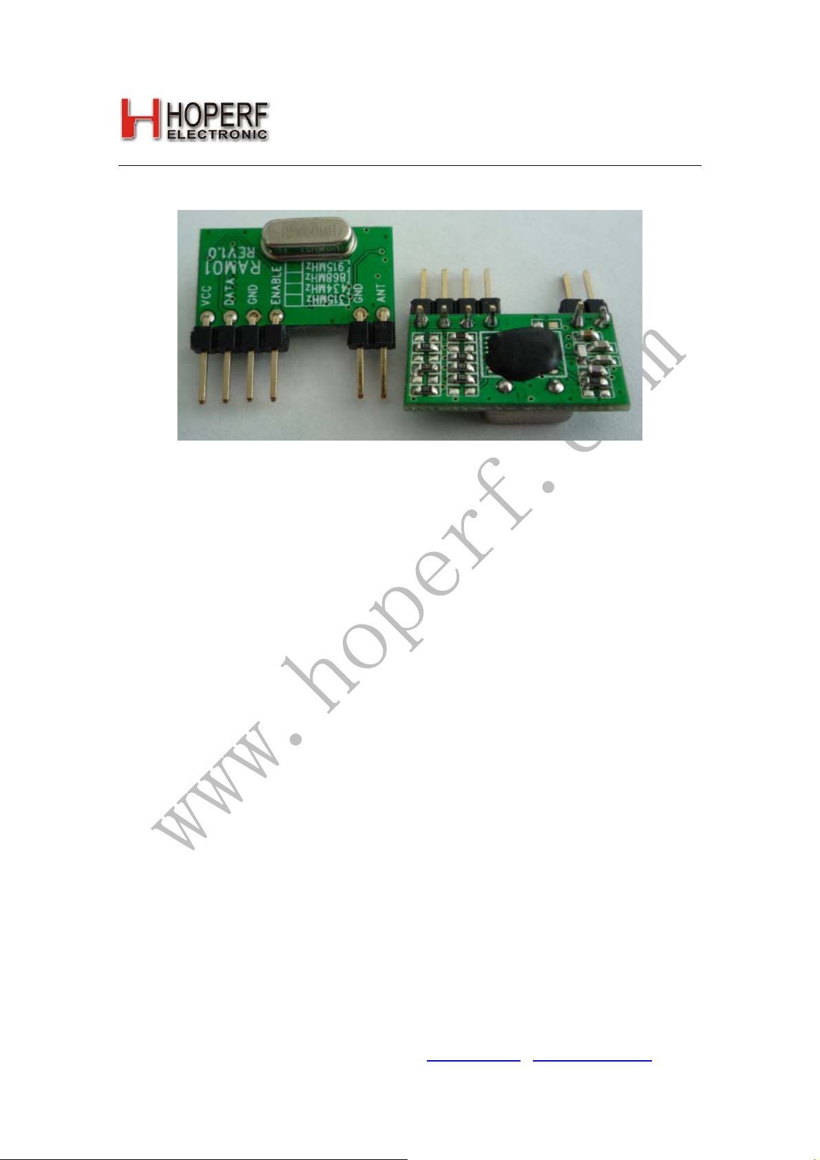
RAM01
RAM01 ISM Band OOK Receiver Module
Version: 1.0 Date: 10/11/2008
DESCRIPTION
HopeRF’s RAM01 is a highly-integrated, low power, multi-channel OOK receiver module designed for use in
applications requiring FCC or ETSI conformance for unlicensed use in the 433, 868 and 915 MHz bands. Used in
conjunction with HopeRF’s transmitters, the RAM01 is a flexible, low cost, and highly integrated solution that does
not require production alignments. All required RF functions are integrated.
The RAM01 has a completely integrated PLL for easy RF design, and its rapid settling time allows for fast frequency
hopping, bypassing multipath fading, and interference to achieve robust wireless links. The PLL’s high resolution
allows the usage of multiple channels in any of the bands. The baseband bandwidth (BW) is programmable to
accommodate various deviations, data rate. The module employs the low-IF approach; therefore, no external
components are needed in a typical application. The RAM01 is a complete analog RF and baseband receiver,
including a multi-band PLL synthesizer with an LNA, down converter mixers, baseband filters and amplifiers, and
demodulator.
The module support Stand alone mode, that means it can receive data without MCU configuration. This mode
mainly simplify the customer application complexity and can be replace traditional super- regenerative receiver and
super-heterodyne receiver.
but frequency can be selected.
for more details about RAM01, please see RA01’s datasheet from http://www.hoperf.com
FEATURES
• Fully integrated receiver module
• No alignment required in production
• Fast settling, programmable, high-resolution PLL
• Fast frequency hopping capability
• Programmable bit rate (up to 40 kbps)
• 50 ohm single-ended antenna input
• Programmable baseband bandwidth (85 to 340 kHz)
• Data filtering and clock recovery
• RX pattern recognition
• SPI compatible serial control interface
• Readable registers
• Clock and reset signals for microcontroller
• 64 bit RX data FIFO
• Accurate Wake-up timer
• Low battery detector
• 2.2 to 3.8 V supply voltage
• Low power consumption
• Low standby current (typ. 0.2 μA)
TYPICAL APPLICATIONS
• Remote control
• Home security and alarm
• Wireless keyboard/mouse and other PC peripherals
• Toy control
• Remote keyless entry
• Tire pressure monitoring
• Telemetry
• Personal/patient data logging
• Remote automatic meter reading
Tel: +86-755-82973805 Fax: +86-755-82973550 E-mail: sales@hoperf.com http://www.hoperf.com
1
Page 2
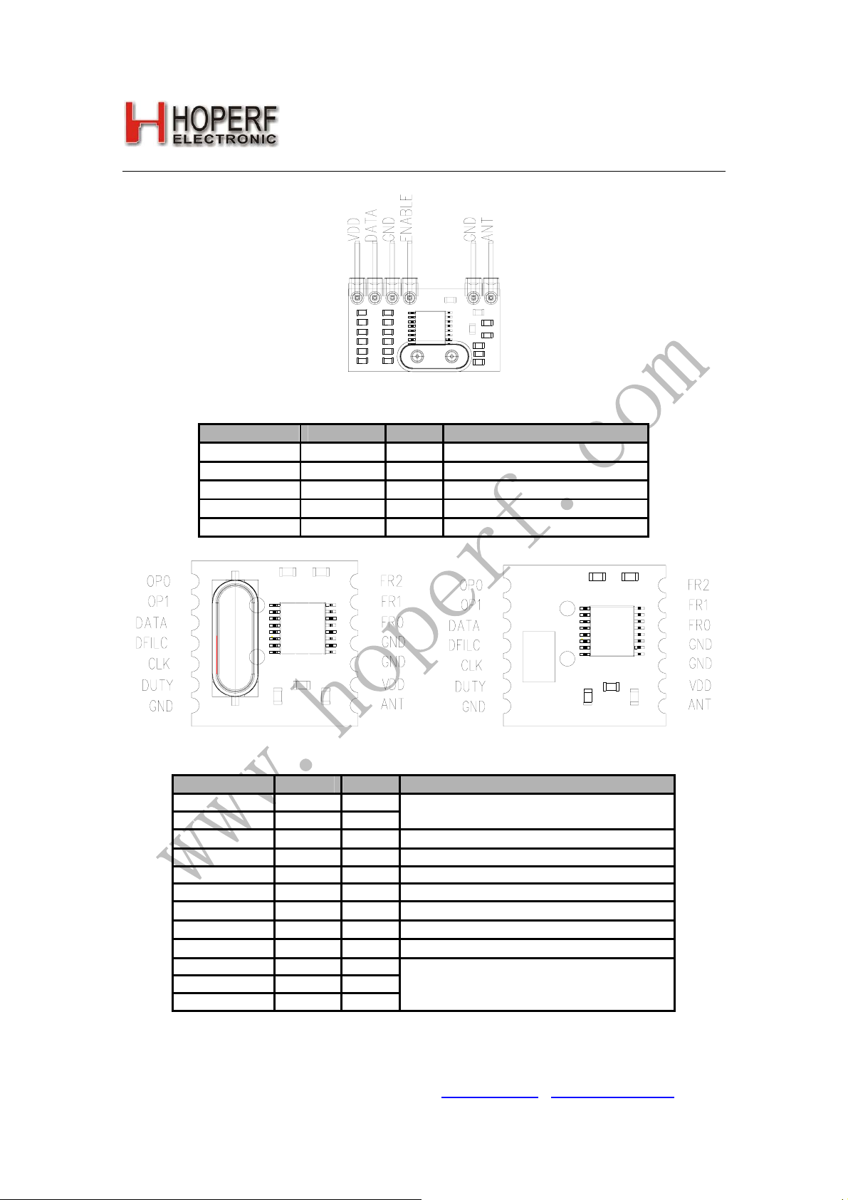
RAM01
Over view and Pin out
Version: 1.0 Date: 10/11/2008
RAM01-D
Pin number Name Type Function
1 VDD P Power supply
2 DATA DO Demodulated data output
3, 5 GND P Ground
4 ENABLE DI Receiving control(active high)
6 ANT AI 50 ohm antenna input
RAM01-S1 RAM01-S2
Pin number Name Type Function
1 OP0 DI
2 OP1 DI
3 DATA DO
4 DFILC AO Data filter capacitor connection
5 CLK DO Divide clock output
6 DUTY DI Duty-cycle mode receiving enable.
7, 10, 11 GND P
8 ANT AI
9 VDD P
12 FR0 DI
13 FR1 DI
14 FR2 DI
Operation frequency band selection pins
Demodulated data output
Ground
50 ohm antenna input
Power supply
Operation frequency selection pins
Tel: +86-755-82973805 Fax: +86-755-82973550 E-mail: sales@hoperf.com http://www.hoperf.com
2
Page 3
RAM01
GENERAL DEVICE SPECIFICATIONS
All voltages are referenced to Vss, the potential on the ground reference pin VSS.
Absolute Maximum Ratings (non-operating)
Symbol Parameter Min Max Units
Vdd Positive supply voltage -0.5 6.0 V
Vin Voltage on any pad -0.5 Vdd+0.5 V
Iin Input current into any pad except VDD and VSS 25 25 mA
ESD Electrostatic discharge with human body model
Tst Storage temperature 55 125
Tld Lead temperature (soldering, max 10 s)
Recommended Operating Range
Symbol Parameter Min Max Units
Vdd Positive supply voltage 2.2 3.8 V
Top Ambient operating temperature 40 +85
ELECTRICAL SPECIFICATION
(Min/max values are valid over the whole recommended operating range, typical conditions: Top = 27 oC; Vdd = Voc =
2.7 V)
DC Characteristics
Symbol Parameter Conditions/Notes Min Typ Max Units
Idd Supply current all bands
Ipd Standby current all blocks disabled
Ilb Low battery voltage detector and
Ix Idle current crystal oscillator is ON
Vlb Low battery detection threshold programmable in 0.1 V steps 2.0 3.5 V
Vlba Low battery detection accuracy ± 2.5 %
VPOR Vdd threshold required
VPOR,hys POR hysteresis larger glithches on the Vdd
SRVdd Vdd slew rate for proper POR generation 0.1 V/ms
Vil Digital input low level 0.3*Vdd V
Vih Digital input high level 0.7*Vdd V
Iil Digital input current Vil = 0 V -1 1 μA
Iih Digital input current Vih = Vdd, Vdd = 3.8 V -1 1 μA
Vol Digital output low level Iol = 2 mA 0.4 V
Voh Digital output high level Ioh = -2 mA Vdd-0.4 V
AC Characteristics
Symbol Parameter Conditions/Notes Min Typ Max Units
fLO Receiver frequency 433 MHz band, 10 kHz resolution
BW Baseband fitler bandwidth mode 1
BRNRZ OOK bit rate with internal digital filters, NRZ data 4.8 40 kbps
BRM OOK bit rate with internal digital filters,
Pmin Receiver sensitivity BER 3* 10-3, BW = 85 kHz, PN9, -110 dBm
wake-up timer current
to generate a POR
1.5 V
generate a POR even above
the threshold V
868 MHz band, 20 kHz resolution
915 MHz band, 20 kHz resolution
mode 2
mode 3
mode 4
mode 5
manchester coded data
POR
Version: 1.0 Date: 10/11/2008
0.6 V
400.96
801.92
881.92
75
125
180
235
305
2.4 20 kbps
1000 V
260
9.6 12 mA
0.2
4
0.5
85
140
200
260
340
439.03
878.06
930.00
95
155
220
295
375
o
C
o
C
o
C
μA
μA
mA
MHz
kHz
Tel: +86-755-82973805 Fax: +86-755-82973550 E-mail: sales@hoperf.com http://www.hoperf.com
3
Page 4

RAM01
BR = 9.6 kbps, Average signal
power
IIP3outh Input IP3 out of band interferers
CCR Co-channel rejection BER = 10-2 with continuous wave
BR100kHz Blocking ratio BER = 10-2 with continuous wave
BR1MHz Blocking ratio same as above,
BR10MHz Blocking ratio same as above,
Pmaxh Maximum input power LNA: high setting
Pmaxa Maximum input power LNA: automatic or low gain setting
Rin RF input impedance real
Cin RF input capacitance 460 fF
RSa RSSI accuracy +/-7 dB
RSr RSSI range With automatic 32 dB LNA gain
RSresp DRSSI response time Until the RSSI output goes high
fref PLL reference frequency (Note 2)
fresLB PLL frequency resolution 434 MHz Band 10 kHz
fresHB PLL frequency resolution 868 MHz or 915 MHz Band 20 kHz
Tsettl PLL settling time Frequency error < 1 kHz
tst1, P PLL startup time Initial calibration after power-up with
Pspur Spurious emission -60 dBm
Cxl Crystal load capacitance,
tPOR Internal POR pulse width
tsx Crystal oscillator startup
tPBt Wake-up timer clock period Calibrated every 30 seconds (Note
twake-up Programmable wake-up
Cin, D Digital input capacitance 2 pF
tr, f Digital output rise/fall time 15 pF pure capacitive load 10 ns
tr, f ,ckout Clock output rise/fall time 10 pF pure capacitive load 15 ns
fckout, slow Slow clock frequency Tolerance +/- 1 kHz 32 kHz
part (differential) (Note 1)
see crystal selection guide
(Note 3)
time
time
Note 1: See matching circuit parameters and antenna design guide for information, and Application Notes available
from http://www.hoperf.com.
Note 2: Using other than a 10 MHz crystal is not recommended because the crystal referred timing and frequency
parameters will change accordingly.
Note 3: During this period, commands are not accepted by the chip.
Note 4: Autocalibration can be turned off.
f-f
LO > 5MHz
interferer in the channel
interferer, BW = 85 kHz,
interferer offset 100 kHz
interferer offset 1 MHz
interferer offset 10 MHz
min 99.99% OOK modulation
min 99.9% OOK modulation
250 Ohm
switch
after the input signal exceeds the
preprogrammed
limit, C
ARRSI = 5nF
after 1 MHz step
running crystal oscillator
Programmable in 0.5 pF steps,
tolerance +/- 10%
After Vdd has reached 90% of final
value
Crystal ESR < 30 Ω 5 ms
4)
1
Version: 1.0 Date: 10/11/2008
-18 dBm
-4 dB
45 dB
50 dB
67 dB
-15 dBm
0 dBm
90 dB
500 μs
30 μs
500 μs
8.5
50 100 ms
0.995 1 1.005 ms
10
16 pF
8.4*10
MHz
6
ms
Tel: +86-755-82973805 Fax: +86-755-82973550 E-mail: sales@hoperf.com http://www.hoperf.com
4
Page 5

RAM01
Application example
a. 4 key single channel remote controller
Version: 1.0 Date: 10/11/2008
Note: This type of RAM01 is use to replace traditional ASK receiver, no any modification of
customer software and hardware. It is a pin-to-pin compliance solution.
b. 8 channel remote controller
Note: This type of RAM01 is designed for more flexible applications witch requiring receiving data
from multi-transmitters, these transmitters send data at different frequency channels. Frequency
channel selection can be done by MCU software or hardware jumpers.
Tel: +86-755-82973805 Fax: +86-755-82973550 E-mail: sales@hoperf.com http://www.hoperf.com
5
Page 6

RAM01
Mechanical information
Version: 1.0 Date: 10/11/2008
RAM01-D
RAM01-S1
Tel: +86-755-82973805 Fax: +86-755-82973550 E-mail: sales@hoperf.com http://www.hoperf.com
6
Page 7

RAM01
RAM01-S2
Ordering information
Part number Package type Frequency band Note
RAM01-433D 433MHz
RAM01-868D 868MHz
RAM01-915D
RAM01-433S1 433MHz
RAM01-868S1 868MHz
RAM01-915S1
RAM01-433S2 433MHz
RAM01-868S2 868MHz
RAM01-915S2
HOPE MICROELECTRONICS CO.,LTD
Address: 4/F, Block B3, East Industrial Area,
Huaqiaochen, Shenzhen, Guangdong, China.
518052
Tel: 86-755-82973805
Fax: 86-755-82973550
Email: sales@hoperf.com
trade@hoperf.com
Website: http://www.hoperf.com
http://www.hoperf.cn
http://hoperf.en.alibaba.com
DIP
SMD
Thin SMD
915MHz
915MHz
915MHz
This document may contain preliminary information and is subject to
change by Hope Microelectronics without notice. Hope
Microelectronics assumes no responsibility or liability for any use of
the information contained herein. Nothing in this document shall
operate as an express or implied license or indemnity under the
intellectual property rights of Hope Microelectronics or third parties.
The products described in this document are not intended for use in
implantation or other direct life support applications where malfunction
may result in the direct physical harm or injury to persons. NO
WARRANTIES OF ANY KIND, INCLUDING, BUT NOT LIMITED TO,
THE IMPLIED WARRANTIES OF MECHANTABILITY OR FITNESS
FOR A ARTICULAR PURPOSE, ARE OFFERED IN THIS
DOCUMENT.
©2008, HOPE MICROELECTRONICS CO.,LTD. All rights reserved.
Version: 1.0 Date: 10/11/2008
Operation frequency channel
should be clarified when
ordering
Operation frequency channel
can be selected by customer
Tel: +86-755-82973805 Fax: +86-755-82973550 E-mail: sales@hoperf.com http://www.hoperf.com
7
 Loading...