

Page 1
RA01
RA01 Universal ISM
Version: 1.0 Date: 10/8/2008
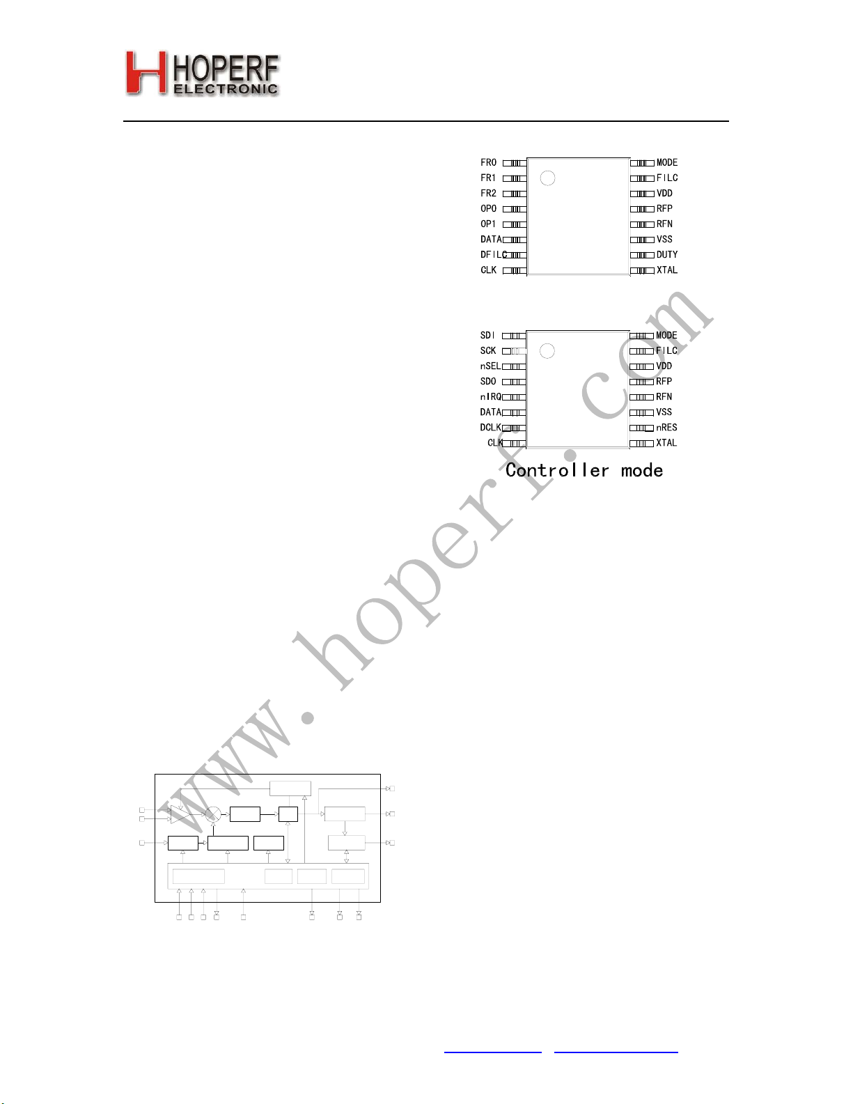
PIN ASSIGNMENT
Band OOK Receiver
DESCRIPTION
HopeRF’s RA01 is a single chip, low power,
multi-channel OOK receiver designed for use in
applications requiring FCC or ETSI conformance for
unlicensed use in the 433, 868 and 915 MHz bands.
Used in conjunction with HopeRF’s transmitters, the
RA01 is a flexible, low cost, and highly integrated
solution that does not require production alignments.
All required RF functions are integrated. Only an
external crystal and few capacitors are needed for
operation.
The RA01 has a completely integrated PLL for easy
RF design, and its rapid settling time allows for fast
frequency hopping, bypassing multipath fading, and
interference to achieve robust wireless links. The
PLL’s high resolution allows the usage of multiple
channels in any of the bands. The baseband
bandwidth (BW) is programmable to accommodate
various deviation, data rate, and crystal tolerance
requirements. The receiver employs the low-IF
approach; therefore, no external components (except
crystal and filtering capacitors) are needed in a typical
application. The RA01 is a complete analog RF and
baseband receiver, including a multi-band PLL
synthesizer with an LNA, down converter mixers,
baseband filters and amplifiers, and demodulator.
The chip dramatically reduces the load on the
microcontroller with integrated digital data processing:
data filtering, clock recovery, data pattern recognition
and integrated FIFO. To minimize the system cost, the
chip can provide a clock signal for the microcontroller,
avoiding the need for two crystals.
BLOCK DIAGRAM
RFP
RFN
XTAL
LNA
CRYSTAL
OSC
CONTROL/STATUS
REGISTER BANK
nSEL SCK SDI SDO MODE nIRQ CLK nRES
CHANNEL
FILTER
PLL
SYNTHESIZER
DIGITAL
CONTROLER
LOW BAT
DETECT
RX DATA
FIFO
GAIN
CONTROL
RSSI
WAKE UP
TIMER
DETECTOR
DATA SLICER
CLOCK
RECOVERY
POWER ON
RESET
RSSI
DATA
DCLK
RA01
Stand alone mode
RA01
FEATURES
• Fully integrated (low BOM, easy design-in)
• No alignment required in production
• Fast settling, programmable, high-resolution PLL
• Fast frequency hopping capability
• Programmable bit rate (up to 40 kbps)
• Direct differential antenna input
• Programmable baseband bandwidth (85 to 340 kHz)
• Analog and digital RSSI outputs
• Data filtering and clock recovery
• RX pattern recognition
• SPI compatible serial control interface
• Readable registers
• Clock and reset signals for microcontroller
• 64 bit RX data FIFO
• Standard 10 MHz crystal reference
• Accurate Wake-up timer
• Low battery detector
• 2.2 to 3.8 V supply voltage
• Low power consumption
• Low standby current (typ. 0.2 μA)
TYPICAL APPLICATIONS
• Remote control
• Home security and alarm
• Wireless keyboard/mouse and other PC peripherals
• Toy control
• Remote keyless entry
• Tire pressure monitoring
• Telemetry
• Personal/patient data logging
• Remote automatic meter reading
Tel: +86-755-82973805 Fax: +86-755-82973550 E-mail: sales@hoperf.com http://www.hoperf.com
1
Page 2
RA01
DETAILED DESCRIPTION
General
The RA01 OOK receiver is a counterpart to the HopeRF
transmitter (e.g. RF02). It covers the unlicensed frequency
bands at 434, 868 and 915 MHz. The device facilitates
compliance with FCC and ETSI requirements.
The programmable PLL synthesizer determines the
operating frequency while preserving accuracy based on
the on-chip crystal controlled reference oscillator. The
PLL’s high resolution allows for the use of multiple
channels in any of the bands.
The receiver employs the low-IF approach with internal
demodulation, allowing the use of a minimal number of
external components in a typical application. The RA01
consists of a fully integrated multi-band PLL synthesizer,
an LNA with switchable gain, down converter mixers,
baseband filters and amplifiers, and an demodulator
followed by a data filter.
LNA
The LNA has 250 Ohm input impedance, which works well
with the recommended antennas. (See Application Notes
available from http://www.hoperf.com.)
If the RF input of the chip is connected to 50 Ohm devices,
an external matching circuit is required to provide the
correct matching and to minimize the noise figure of the
receiver.
The LNA gain (and linearity) can be selected (0, –32 dB)
relative to the highest gain) according to RF signal
strength. This is useful in an environment with strong
interferers.
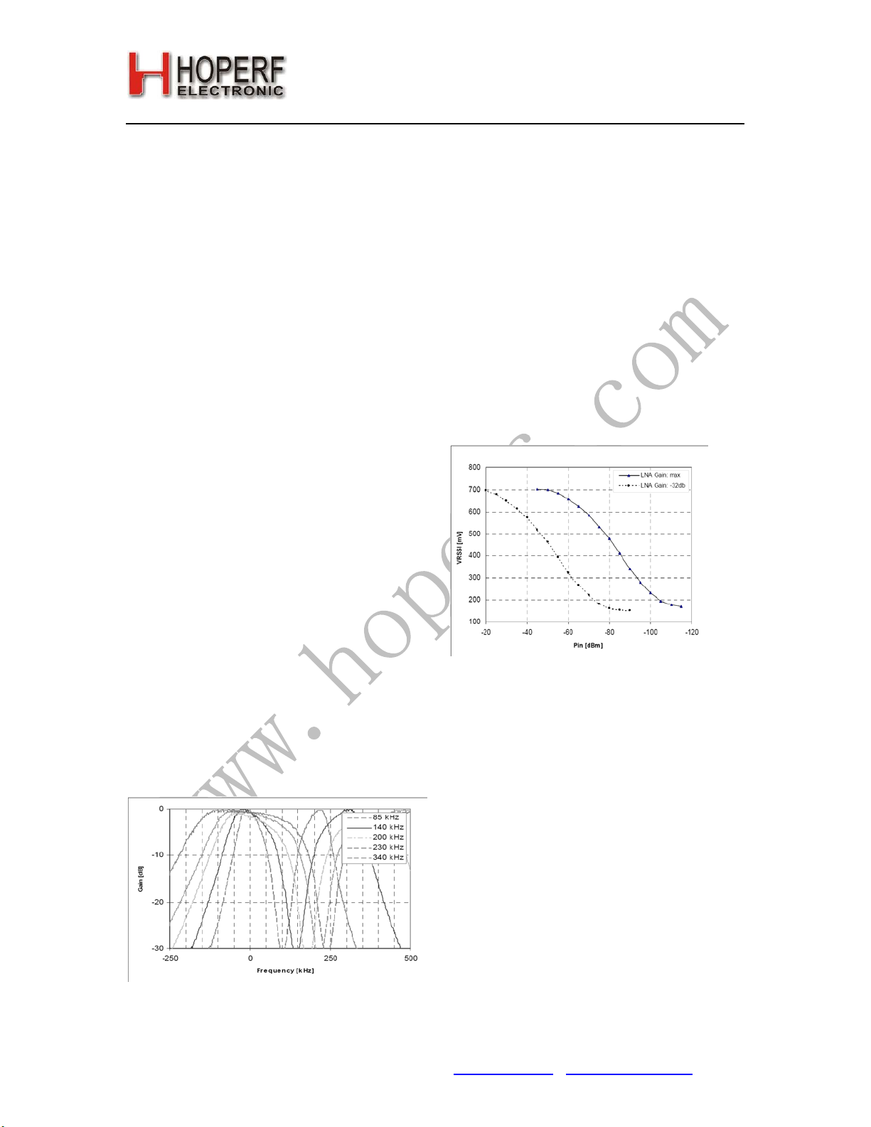
Baseband Filters
The receiver bandwidth is selectable by programming the
bandwidth (BW) of the baseband filters. This allows
setting up the receiver according to the characteristics of
the signal to be received.
An appropriate bandwidth can be selected to
accommodate various OOK deviation, data rate, and
crystal tolerance requirements. The filter structure is a 7th
order Butterworth low-pass with 40 dB suppression at
2*BW frequency. Offset cancellation is accomplished by
using a high-pass filter with a 90 kHz cut-off frequency.
Filter bandwidth is measured between the 6dB attenuation
points.
Typical Baseband Filter Characteristics
Data Filtering and Clock Recovery
The output data filtering can be completed by an
external capacitor to the final application.
Analog operation: The filter is an RC type low-pass
filter and a Schmitt-trigger (St). The resistor (10k) and
the St is integrated on the chip. An (external) capacitor
can be chosen according to the
actual bit-rate.
Data Validity Blocks / Demodulator
RSSI
A digital RSSI output is provided to monitor the input
signal level. It goes to an comparator, if the received
signal strength exceeds a given preprogrammed level
an internal -32dB attenuator is activated in the LNA.
The RSSI settling time depends on the filter capacitor
used.
Typical Analog RSSI Voltage vs. RF Input Power
Crystal Oscillator and
Microcontroller Clock Output
The chip has a single-pin crystal oscillator circuit,
which provides a 10 MHz reference signal for the PLL.
To reduce external parts and simplify design, the
crystal load capacitor is internal and programmable.
Guidelines for selecting the appropriate crystal can
be found later in this datasheet. The receiver can
supply the clock signal for the microcontroller, so
accurate timing is possible without the need for a
second crystal. In normal operation it is divided from
the reference 10 MHz. During sleep mode a low
frequency (typical 32 kHz) output clock signal can be
switched on.
When the microcontroller turns the crystal oscillator off
by clearing the appropriate bit using the
Setting Command,
number (default is 128) of further clock pulses (“clock
tail”) for the microcontroller to let it go to idle or sleep
mode.
Version: 1.0 Date: 10/8/2008
Configuration
the chip provides a programmable
Tel: +86-755-82973805 Fax: +86-755-82973550 E-mail: sales@hoperf.com http://www.hoperf.com
2
Page 3

RA01
Low Battery Voltage Detector
The low battery detector circuit monitors periodically (typ.
8 ms) the supply voltage and generates an interrupt if it
falls below a programmable threshold level.
Wake-Up Timer
The wake-up timer has very low current consumption (4
μA max) and can be programmed from 1 ms to several
hours.
It calibrates itself to the crystal oscillator at every startup
and then at every 30 seconds with an accuracy of ±0.5%.
When the crystal oscillator is switched off, the calibration
circuit switches it back on only long enough for a quick
calibration (a few milliseconds) to facilitate accurate
wake-up timing. The periodic auto-calibration feature can
be turned off.
Event Handling
In order to minimize current consumption, the receiver
supports the sleep mode. Active mode can be initiated by
setting the ex or en bits (in the Configuration Setting or
Receiver Setting Command).
RA01 generates an interrupt signal on several events
(wake-up timer timeout, low supply voltage detection,
on-chip FIFO filled up). This signal can be used to wake
up the microcontroller, effectively reducing the period the
microcontroller has to be active. The cause of the interrupt
can be read out from the receiver by the microcontroller
through the SDO pin.
Interface and Controller
An SPI compatible serial interface lets the user select the
frequency band, center frequency of the synthesizer, and
the bandwidth of the baseband signal path. Division ratio
for the microcontroller clock, wake-up timer period, and
low supply voltage detector threshold are also
programmable. Any of these auxiliary functions can be
disabled when not needed. All parameters are set to
default after power-on; the programmed values are
retained during sleep mode. The interface supports the
read-out of a status register, providing detailed
information about the status of the receiver and the
received data. It is also possible to store the received data
bits into the 64 bit RX FIFO register and read them out in a
buffered mode. FIFO mode can be enabled through the
SPI compatible interface by setting the fe bit to 1 in the
Output and FIFO Mode Command. During FIFO read the
crystal oscillator must be ON.
Version: 1.0 Date: 10/8/2008
Tel: +86-755-82973805 Fax: +86-755-82973550 E-mail: sales@hoperf.com http://www.hoperf.com
3
Page 4
RA01
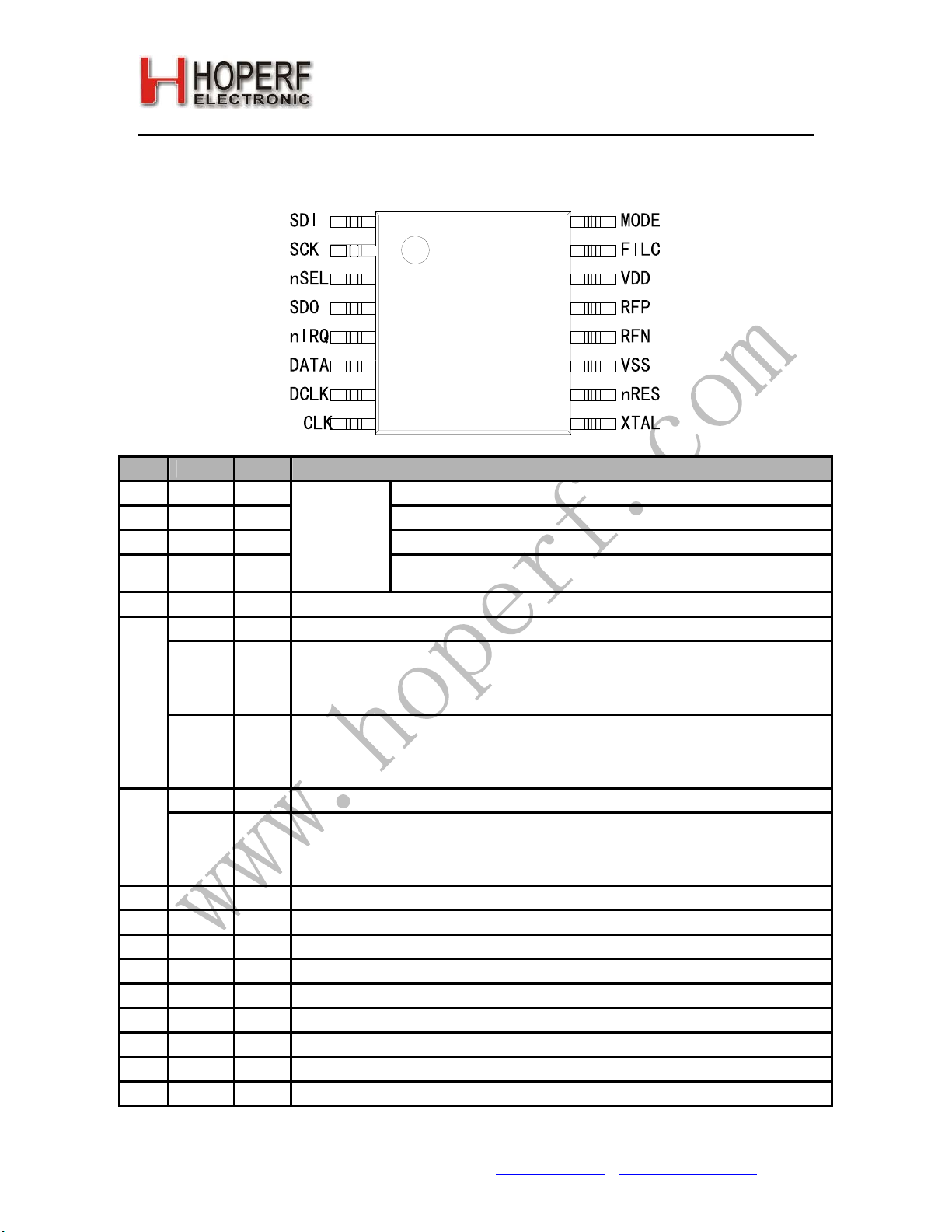
PIN DEFINITIONS
A=analog, D=digital, S=supply, I=input, O=output, IO=input / output
Controller Mode
RA01
Version: 1.0 Date: 10/8/2008
Pin Name Type Function
1 SDI DI Serial data input
2 SCK DI Serial clock input
3 nSEL DI Select input (active low)
4 SDO DO
5 nIRQ DO
DATA DO
nFFS DI
6
DFILC AIO
DCLK DO
7
FFIT DO
8 CLK DO
9 XTAL AIO
10 nRES DO
11 VSS S
12 RFN AI
13 RFP AI
14 VDD S
15 FILC AIO
16 MODE DI
SPI
interface
Serial data output (tri-state if SPI bus is not selected, internal
bus-hold cell)
Interrupt request output (active low)
Demodulated data output
FIFO direct select input, with internal pull-up.
Conditions:
ef
= high in
sf = low
Note: 6 Value of the internal pull up resistor is 120 kOhm.
Data Filter Capacitor connection
Conditions:
ef
= low in
sf =
Note: If this bit is set the internal clock recovery and the FIFO is not usable.
Recovered data clock output for bit sampling
FIFO interrupt output
High when the number of the bits in the RX FIFO has reached the preprogrammed limit.
Conditions:
ef
= high in
sf =
Microcontroller clock output (optional)
Reference crystal connection
Power-on reset output (active low, optional)
Supply ground reference
Differential RF (antenna) input
Differential RF (antenna) input
Positive supply voltage
Filter capacitor connection (See
Mode select input. High=microcontroller mode
Output and FIFO mode Command.
in the
Data Filter Command
Output and FIFO mode Command.
high in the
low in the
Data Filter Command
Output and FIFO mode Command.
Data Filter Command
.
.
.
Demodulator Setting Command
for details)
Tel: +86-755-82973805 Fax: +86-755-82973550 E-mail: sales@hoperf.com http://www.hoperf.com
4
Page 5
RA01
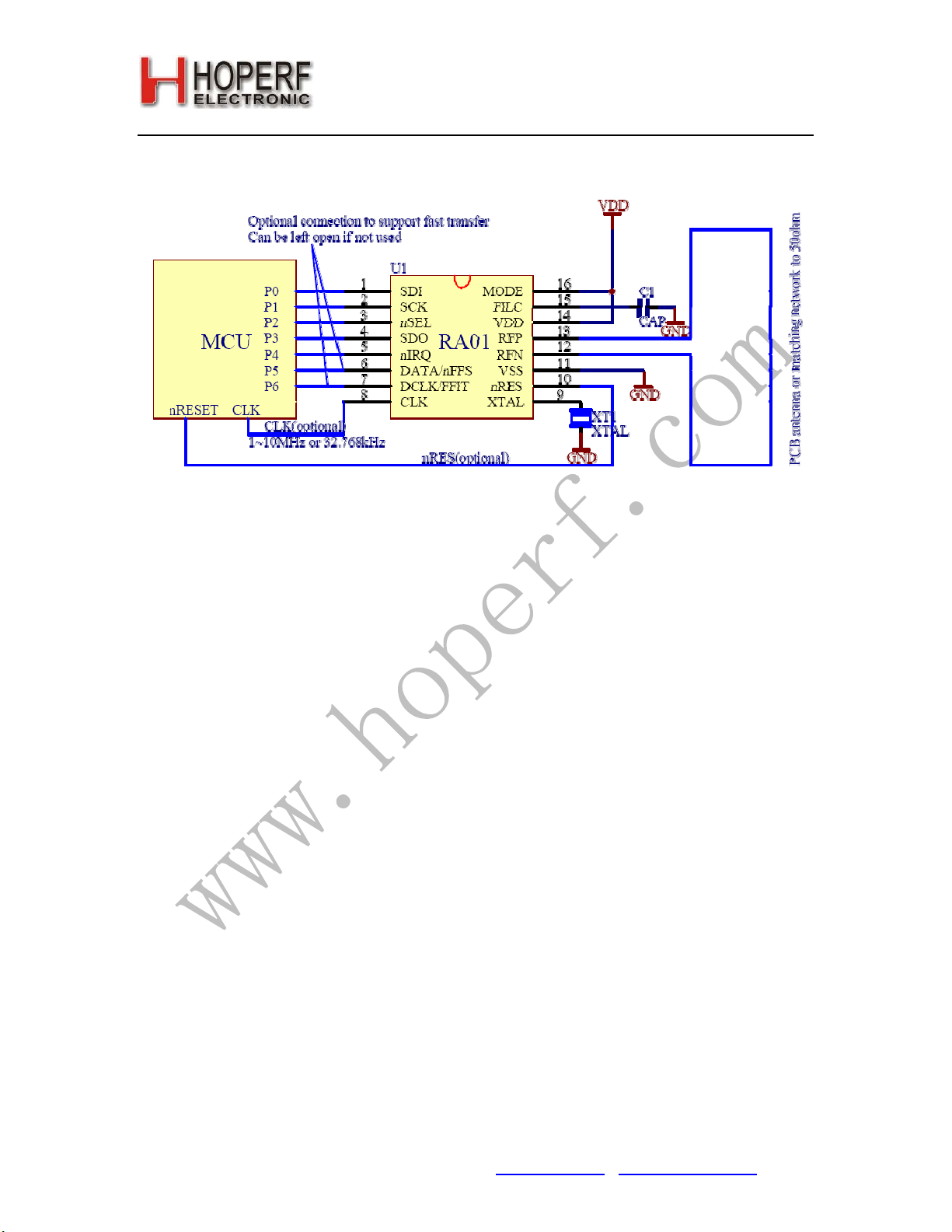
Typical Application
Typical application with FIFO usage
Version: 1.0 Date: 10/8/2008
Tel: +86-755-82973805 Fax: +86-755-82973550 E-mail: sales@hoperf.com http://www.hoperf.com
5
Page 6
RA01
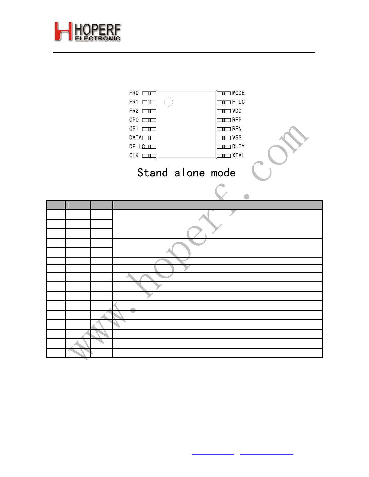
Standalone Mode
RA01
Version: 1.0 Date: 10/8/2008
Pin Name Type Function
1 FR0 DI
2 FR1 DI
3 FR2 DI
4 OP0 DO
5 OP1 DO
6 DATA DO
7 DFILC AIO
8 CLK DO
9 XTAL AIO
10 DUTY DI
11 VSS S
12 RFN AI
13 RFP AI
14 VDD S
15 FILC AIO
16 MODE DI
Receiving frequency setting inputs
Operation mode select:
00: Shutdown, 01:433MHz band, 10: 868MHz band, 11: Reserved
Demodulated data output
Data filter capacitor connection (See
Microcontroller clock output (optional)
Reference crystal connection
Low duty cycle rx mode
Supply ground reference
Differential RF (antenna) input
Differential RF (antenna) input
Positive supply voltage
Filter capacitor connection (See
Mode select input. Low=stand alone mode
Data Filter Command
Demodulator Setting Command
for details)
for details)
Tel: +86-755-82973805 Fax: +86-755-82973550 E-mail: sales@hoperf.com http://www.hoperf.com
6
Page 7

RA01
GENERAL DEVICE SPECIFICATIONS
All voltages are referenced to Vss, the potential on the ground reference pin VSS.
Absolute Maximum Ratings (non-operating)
Symbol Parameter Min Max Units
Vdd Positive supply voltage -0.5 6.0 V
Vin Voltage on any pad -0.5 Vdd+0.5 V
Iin Input current into any pad except VDD and VSS 25 25 mA
ESD Electrostatic discharge with human body model
Tst Storage temperature 55 125 oC
Tld Lead temperature (soldering, max 10 s)
Recommended Operating Range
Symbol Parameter Min Max Units
Vdd Positive supply voltage 2.2 3.8 V
Top Ambient operating temperature 40 +85 oC
ELECTRICAL SPECIFICATION
(Min/max values are valid over the whole recommended operating range, typical conditions: Top = 27 oC; Vdd = Voc =
2.7 V)
DC Characteristics
Symbol Parameter Conditions/Notes Min Typ Max Units
Idd Supply current all bands
Ipd Standby current all blocks disabled
Ilb Low battery voltage detector and
wake-up timer current
Ix Idle current crystal oscillator is ON
Vlb Low battery detection threshold programmable in 0.1 V steps 2.0 3.5 V
Vlba Low battery detection accuracy ± 2.5 %
VPOR Vdd threshold required
to generate a POR
VPOR,hys POR hysteresis larger glithches on the Vdd
SRVdd Vdd slew rate for proper POR generation 0.1 V/ms
Vil Digital input low level 0.3*Vdd V
Vih Digital input high level 0.7*Vdd V
Iil Digital input current Vil = 0 V -1 1 μA
Iih Digital input current Vih = Vdd, Vdd = 3.8 V -1 1 μA
Vol Digital output low level Iol = 2 mA 0.4 V
Voh Digital output high level Ioh = -2 mA Vdd-0.4 V
1.5 V
generate a POR even above
the threshold V
POR
Version: 1.0 Date: 10/8/2008
0.6 V
1000 V
260 oC
9.6 12 mA
0.2
4
0.5
μA
μA
mA
Tel: +86-755-82973805 Fax: +86-755-82973550 E-mail: sales@hoperf.com http://www.hoperf.com
7
Page 8

RA01
DC Characteristics
Symbol Parameter Conditions/Notes Min Typ Max Units
fLO Receiver frequency 433 MHz band, 10 kHz resolution
BW Baseband fitler bandwidth mode 1
BRNRZ OOK bit rate with internal digital filters, NRZ data 4.8 40 kbps
BRM OOK bit rate with internal digital filters,
Pmin Receiver sensitivity BER 3* 10-3, BW = 85 kHz, PN9,
IIP3outh Input IP3 out of band interferers
CCR Co-channel rejection BER = 10-2 with continuous wave
BR100kHz Blocking ratio BER = 10-2 with continuous wave
BR1MHz Blocking ratio same as above,
BR10MHz Blocking ratio same as above,
Pmaxh Maximum input power LNA: high setting
Pmaxa Maximum input power LNA: automatic or low gain setting
Rin RF input impedance real
Cin RF input capacitance 460 fF
RSa RSSI accuracy +/-7 dB
RSr RSSI range With automatic 32 dB LNA gain
RSresp DRSSI response time Until the RSSI output goes high
fref PLL reference frequency (Note 2) 9.5 10 10.5 MHz
fresLB PLL frequency resolution 434 MHz Band 10 kHz
fresHB PLL frequency resolution 868 MHz or 915 MHz Band 20 kHz
Tsettl PLL settling time Frequency error < 1 kHz
tst1, P PLL startup time Initial calibration after power-up with
Pspur Spurious emission -60 dBm
Cxl Crystal load capacitance,
tPOR Internal POR pulse width
tsx Crystal oscillator startup
tPBt Wake-up timer clock period Calibrated every 30 seconds (Note
twake-up Programmable wake-up
Cin, D Digital input capacitance 2 pF
tr, f Digital output rise/fall time 15 pF pure capacitive load 10 ns
tr, f ,ckout Clock output rise/fall time 10 pF pure capacitive load 15 ns
fckout, slow Slow clock frequency Tolerance +/- 1 kHz 32 kHz
part (differential) (Note 1)
see crystal selection guide
(Note 3)
time
time
868 MHz band, 20 kHz resolution
915 MHz band, 20 kHz resolution
mode 2
mode 3
mode 4
mode 5
manchester coded data
BR = 9.6 kbps, Average signal
power
f-f
LO > 5MHz
interferer in the channel
interferer, BW = 85 kHz,
interferer offset 100 kHz
interferer offset 1 MHz
interferer offset 10 MHz
min 99.99% OOK modulation
min 99.9% OOK modulation
250 Ohm
switch
after the input signal exceeds the
preprogrammed
limit, C
ARRSI = 5nF
after 1 MHz step
running crystal oscillator
Programmable in 0.5 pF steps,
tolerance +/- 10%
After Vdd has reached 90% of final
value
Crystal ESR < 30 Ω 5 ms
4)
1
Version: 1.0 Date: 10/8/2008
400.96
801.92
881.92
75
125
180
235
305
2.4 20 kbps
-110 dBm
-18 dBm
-4 dB
45 dB
50 dB
67 dB
-15 dBm
85
140
200
260
340
439.03
878.06
930.00
95
155
220
295
375
0 dBm
90 dB
500 μs
30 μs
500 μs
8.5
50 100 ms
0.995 1 1.005 ms
16 pF
8.4*10
MHz
kHz
6
ms
Tel: +86-755-82973805 Fax: +86-755-82973550 E-mail: sales@hoperf.com http://www.hoperf.com
8
Page 9

RA01
Note 1: See matching circuit parameters and antenna design guide for information, and Application Notes available
from http://www.hoperf.com.
Note 2: Using other than a 10 MHz crystal is not recommended because the crystal referred timing and frequency
parameters will change accordingly.
Note 3: During this period, commands are not accepted by the chip.
Note 4: Autocalibration can be turned off.
CONTROL INTERFACE
Commands to the receiver are sent serially. Data bits on pad SDI are shifted into the device upon the rising edge of the
clock on pad SCK whenever the chip select pad nSEL is low. When the nSEL signal is high, it initializes the serial interface.
The number of bits sent is an integer multiple of 8. All commands consist of a command code, followed by a varying
number of parameter or data bits. All data are sent MSB first (e.g. bit 15 for a 16-bit command). Bits having no influence
(don’t care) are indicated with X. The Power On Reset (POR) circuit sets default values in all control registers.
The receiver will generate an interrupt request (IRQ) for the microcontroller on the following events:
• Supply voltage below the preprogrammed value is detected (LBD)
• Wake-up timer timeout (WK-UP)
• FIFO received the preprogrammed amount of bits (FFIT)
• FIFO overflow (FFOV)
FFIT and FFOV are applicable only when the FIFO is enabled. To find out why the nIRQ was issued, the status bits should
be read out.
Timing Specification
Symbol Parameter Minimum value [ns]
tCH Clock high time 25
tCL Clock low time 25
tSS Select setup time (nSEL falling edge to SCK rising edge) 10
tSH Select hold time (SCK falling edge to nSEL rising edge) 10
tSHI Select high time 25
tDS Data setup time (SDI transition to SCK rising edge) 5
tDH Data hold time (SCK rising edge to SDI transition) 5
tOD Data delay time 10
Timing Diagram
Version: 1.0 Date: 10/8/2008
tSS
nSEL
tOD
SCK
SDI
SDO
tCH
tCL
tDH
tDS
BIT15 BIT14 BIT13 BIT8 BIT7 BIT1 BIT0
BIT15 BIT14 BIT13 BIT8 BIT7 BIT1 BIT0
Tel: +86-755-82973805 Fax: +86-755-82973550 E-mail: sales@hoperf.com http://www.hoperf.com
tSHI
tSH
9
Page 10

RA01
Control Commands
Control Word Related Parameters/Functions Related control bits
Configuration Setting Command Frequency band, crystal oscillator load
1
Frequency Setting Command Frequency of the local oscillator f11 to f0
2
Receiver Setting Command VDI source, LNA gain, squelch, enable receiver d1 to d0, g1 to g0, sq, en
3
Wake-up Timer Command Wake-up time period r3 to r0, m7 to m0
4
Extended Wake-up Timer Command Wake-up time period finer adjustment d1 to d0, m13 to m8
5
Low Battery Detector
6
and Clock Divider Command
Data Filter Command Data filter type, clock recovery parameters, POR
7
Data Rate Command Bit rate cs, r6 to r0
8
Output and FIFO Command FIFO IT level, FIFO start control, FIFO enable
9
Extended Features Command Low frequency output clock, wake-up timer extra
10
Low Duty Cycle Command Duty Cycle operation d6 to d0, enld
11
Demodulator Setting Command Demodulator time constant tc1, tc0
12
Status Read Command Receiver status read
13
Note: In the following tables the POR column shows the default values of the command registers after power-on.
1. Configuration Setting Command
bit 15 14 13 12 11 10 9 8 7 6 5 4 3 2 1 0 POR
1 0 0 b1 b0 eb et ex x3 x2 x1 x0 i2 i1 i0 dc 938Ah
b1 b0 Frequency Band [MHz]
0 0 Reserved
0 1 434
1 0 868
1 1 915
i2 i1 i0 IF Frequency
0 0 0 Reserved Reserved
0 0 1 245 340
0 1 0 230 260
0 1 1 180 200
1 0 0 145 140
1 0 1 105 105
1 1 0 Reserved Reserved
1 1 1 Reserved Reserved
Note: The wake-up timer can be enabled by the
Divider Command or by the
enldc
bit in the Low Duty Cycle Command or by enabling the low battery detector by
[kHz]
capacitance, baseband filter bandwidth, etc.
LBD voltage and microcontroller clock division
ratio
level selection, autosleep mode
and FIFO fill enable
functions, long FIFO extra functions
Baseband
Bandwidth [kHz]
elfc
Bits eb and et control the operation of the low battery
detector and wake-up timer, respectively. They are
enabled when the corresponding bit is set.
If ex is set the crystal is active during non-active
mode. When dc bit is set it disables the clock output.
bit in the Low Battery Detector and Microcontroller Clock
Version: 1.0 Date: 10/8/2008
b1 to b0, eb, et, x3 to x0,
x3 x2 x1 x0 Crystal Load
0 0 0 0 8.5
0 0 0 1 9.0
0 0 1 0 9.5
0 0 1 1 10.0
i2 to i0. dc
d2 to d0, elfc, t3 to t0
al, ml, dsfi, sf, ewl, srt, r1
to r0
f3 to f0, s1 to s0, ff, fe
exlp, ctls, dcal, bw1 to
bw0, f5 to f4
Capacitance [pF]
… …
0 0 0 0 15.5
0 0 0 0 16.0
eb
bit in this command.
Tel: +86-755-82973805 Fax: +86-755-82973550 E-mail: sales@hoperf.com http://www.hoperf.com
10
Page 11

RA01
2. Frequency Setting Command
bit 15 14 13 12 11 10 9 8 7 6 5 4 3 2 1 0 POR
1 0 1 0 f11 f10 f9 f8 f7 f6 f5 f4 f3 f2 f1 f0 AD57h
The 12-bit Frequency Setting Command <f11 :
f0> has the value F. The value F should be in the
range of 96 and 3903. When F is out of range, the
previous value is kept. The synthesizer center
frequency f
0 = R * 10 MHz * (C + F/4000)
f
0 can be calculated as:
3. Receiver Setting Command
bit 15 14 13 12 11 10 9 8 7 6 5 4 3 2 1 0 POR
1 1 0 0 0 0 0 0 d1 d0 g1 g0 sq 0 0 en C080h
Bit 7-6 <
d1:d0
>: Select the VDI (valid data indicator) signal:
Bit 5-4 <
g1:g0
>: Set the LNA gain:
Bit 3 <sq>: Enables the squelch function. Disables the signals on pin 6 (data) and pin 7 (data clk) when VDI is low.
en
Bit 0 <
and the low battery detector are not affected by this setting.
>: Enables the whole receiver chain and crystal ocsillator when set. Enable/disable of the wake-up timer
4. Wake-up Timer Command
bit 15 14 13 12 11 10 9 8 7 6 5 4 3 2 1 0 POR
1 1 1 0 r3 r2 r1 r0 m7 m6 m5 m4 m3 m2 m1 m0 E196h
The wake-up time period can be calculated by M <
Note: The wake-up timer generates interrupts continuously at the programmed interval while the
5. Extended Wake-up Timer Command
bit 15 14 13 12 11 10 9 8 7 6 5 4 3 2 1 0 POR
1 1 0 0 0 0 1 1 d1 d0 m13 m12 m11 m10 m9 m8 C300h
These bits can be used for further fine adjustment of the wake-up timer. The explanation of the bits can be found
above.
The constant C is determined by the selected
band as:
Band [MHz] R C
433 4 5
868 8 10
d1 d0 VDI output
0 0 RSSI or Clock Recovery Lock
0 1 RSSI
1 0 Clock Recovery Lock
1 1 Always High
g1 g0 GLNA (dB relative to max. G)
0 X Automatic Gain Switch
1 0 -32
1 1 0
m13 : m0
wake-up = M * 2
T
> , R <
R-D
Version: 1.0 Date: 10/8/2008
r3 : r0
ms
> and D <
d1 : d0
>:
et
bit is set.
Tel: +86-755-82973805 Fax: +86-755-82973550 E-mail: sales@hoperf.com http://www.hoperf.com
11
Page 12

RA01
6. Low Battery Detector and Microcontroller Clock Divider Command
bit 15 14 13 12 11 10 9 8 7 6 5 4 3 2 1 0 POR
1 1 0 0 0 0 1 0 d2 d1 d0 elfc t3 t2 t1 t0 C213h
Bit 7-5 <d2-d0>: Clock divider configuration (valid only if the crystal oscillator is on):
elfc
Bit 4 <
Bits 3-0 <t3-t0>: Determines the threshold voltage of the threshold voltage V
>: Enables low frequency (32 kHz) microcontroller output clock during sleep mode.
7. Data Filter Command
bit 15 14 13 12 11 10 9 8 7 6 5 4 3 2 1 0 POR
1 1 0 0 0 1 0 0 al ml dsfi sf ewi srt 1 0 C462h
Bit 7 <al>: Clock recovery (CR) auto lock control if set. It means that the CR start in fast mode after locking it
automatically switches to slow mode.
ml
Bit 6 <
slow release
Using the slower one requires more accurate bit timing (see
Bit 5 <
Bit 4 <
Digital: this is a digital realization of an analog RC filter followed by a comparator with hysteresis. The time constant
is automatically adjusted to the bit rate defined by the
The table shows the optimal filter capacitor values for different data rates
Note: If analog RC filter is selected the internal clock recovery circuit and the FIFO can not be used.
Bit 3 <
Bit 2 <srt>: Resets the bit slicer capacitor.
>: Clock recovery lock control 1: fast mode, fast attack and fast release - 0: slow mode, slow attack and
dsfi
>: Disables autosleep on FIFO interrupt if set to 1.
sf
>: Selects the type of the data filter:
ewi
>: Enables the automatic wake-up on any interrupt event.
d2 d1 d0 Clock Output Frequency [MHz]
0 0 0 1
0 0 1 1.25
0 1 0 1.66
0 1 1 2
1 0 0 2.5
1 0 1 3.33
1 1 0 5
1 1 1 10
lb= 2.0 V + T * 0.1 V
V
Data Rate Command
sf Filter Type
0 Digital Filter
1 Analog Filter with external
capacitor on pin7
Data Rate Command
4.8 kbps 9.6 kbps 19.2 kbps 38.4 kbps
6.8 nF 3.3 nF 1.5 nF 680 pF
Version: 1.0 Date: 10/8/2008
lb of the detector:
).
.
Tel: +86-755-82973805 Fax: +86-755-82973550 E-mail: sales@hoperf.com http://www.hoperf.com
12
Page 13

RA01
8. Data Rate Command
bit 15 14 13 12 11 10 9 8 7 6 5 4 3 2 1 0 POR
1 1 0 0 1 0 0 0 cs r6 r5 r4 r3 r2 r1 r0 C813h
The expected bit rate of the received data stream is determined by the 7-bit value R (bits
BR = 10 MHz / 29 / (R+1) / (
In the receiver set R according the next function:
R= (10 MHz / 29 /(
Apart from setting custom values, the standard bit rates from 600 bps to 115.2 kbps can be approximated with small
error.
Data rate accuracy requirements:
Clock recovery in slow mode:
BR is the bit rate set in the receiver and
maximal number of consecutive ones or zeros in the data stream. It is recommended for long data packets to
include enough 1/0 and 0/1 transitions, and be careful to use the same division ratio in the receiver and in the
transmitter.
ΔBR is a theoretical limit for the clock recovery circuit. Clock recovery will not work above this limit. The clock
recovery circuit will always operate below this limit independently from process, temperature, or Vdd condition.
e.g. Supposing a maximum length of consecutive zeros or ones in the data stream is less than 5 bits, the necessary
relative accuracy is 0.68% in slow mode and 2.1% in fast mode.
1 + cs
9. Output and FIFO Mode Command
bit 15 14 13 12 11 10 9 8 7 6 5 4 3 2 1 0 POR
1 1 0 0 1 1 1 0 f3 f2 f1 f0 s1 s0 ff fe CE87h
Bit 7-4 <
Bit 3-2 <
Note: VDI (Valid Data Indicator) see further details in
mode is 2DD4h.
Bit 1 <
Bit 0 <
Note: To restart the synchron word reception, bit 1 should be cleared and set. This action will initialize the FIFO and
clear its content.
Bit 0 modifies the function of DATA pad and DCLK pad. The DATA pad will become input (nFFS) if
If the chip is used in FIFO mode, do not allow this to be a floating input.
f3 : f0
>: FIFO IT level. The FIFO generates IT when number of the received data bits reaches this level.
s1 : s0
>: Select the input of the FIFO fill start condition:
ff
>: Enables FIFO fill after synchron word reception. FIFO fill stops when this bit is cleared.
fe
>: Enables the 64 bit deep FIFO mode. To clear the counter of the FIFO, it has to be set to zero.
1 + cs
*7)
*7)/ BR) – 1
ΔBR/BR < 1/(29*Nbit) Clock recovery in fast mode: ΔBR/BR < 3/(29*Nbit)
ΔBR is bit rate difference between the transmitter and the receiver. Nbit is the
s1 s0 FIFO fill starts
0 0 VDI
0 1
1 0
1 1 Always fill
Sync. Word
Receiver Setting Command
Version: 1.0 Date: 10/8/2008
r6
to r0) and the 1 bit cs.
, Synchron word in microcontroller
fe
is set to 1.
Tel: +86-755-82973805 Fax: +86-755-82973550 E-mail: sales@hoperf.com http://www.hoperf.com
13
Page 14

RA01
10. Extended Features Command
bit 15 14 13 12 11 10 9 8 7 6 5 4 3 2 1 0 POR
1 0 1 1 0 0 0 0 exlp ctls 0 dcal bw1 bw0 f5 f4 B0CAh
Bit 7 <
exlp
Bit 6 <
Bit 4 <
Bit 3-2 <
>: Enables low power mode for the crystal oscillator.
ctls
>: Clock tail selection bit. Setting this bit selects 512 bit long clock tail instead of the default 128 bit length.
dcal
>: Disables the wake-up timer auto calibration.
bw1:bw0
>: Select the bandwidth of the PLL.
Bit 1-0 <
FIFO Mode Command.
f5:f4
>: Upper two bits for selecting the 64 bit FIFO IT level together with the
11. Low Duty Cycle Command
bit 15 14 13 12 11 10 9 8 7 6 5 4 3 2 1 0 POR
1 0 1 1 0 0 0 0 d6 d5 d4 d3 d2 d1 d0 enld B0CAh
Bit 7-1 <
Timer Command
Duty-Cycle= (D * 2 +1) / M *100%
Bit 0 <
d6:d1
>: The Duty-Cycle can be calculated by using D (
.)
enld
>: Enables the low duty cycle operation of the receiver.
12. Demodulator Setting Command
bit 15 14 13 12 11 10 9 8 7 6 5 4 3 2 1 0 POR
1 0 1 1 0 0 0 0 tc1 tc0 0 0 0 0 0 0 D000h
Bit 7-6 <
The table shows the optimal filter capacitor values for different popular data rates:
Note: Manchester coding doubles the bandwidth requirement compared to NRZ.
tc1:tc0
>: Select the time constant of the demodulator
Data Rate [kbps] Manchester 2.4 4.8 9.6 19.2 38.4 >38.4
Data Rate [kbps] NRZ - 2.4 4.8 9.6 19.2 >19.2
Recommended Capacitor on pin15 ( FILC) [pF] 330 330 220 100 27 0
Optimal <tc1:tc0> setting Slow Slow Middle Middle Fast Fast
bw1 bw0 PLL bandwidth
0 0 15 kHz
0 1 30 kHz
1 0 60 kHz
1 1 120 kHz
d6
tc1 tc0 Time constant
0 0 Fast
1 1 Middle
1 0 Slow
1 1 Reserved
Version: 1.0 Date: 10/8/2008
f3-f0
bits in the Output and
to d0) and M. (M is parameter in a
Wake-Up
Tel: +86-755-82973805 Fax: +86-755-82973550 E-mail: sales@hoperf.com http://www.hoperf.com
14
Page 15

RA01
13. Status Read Command
The read command starts with a zero, whereas all other control commands start with a one. Therefore, after
receiving the first bit of the control command the RA01 identifies it as a read command. So as the first bit of the
command is received, the receiver starts to clock out the status bits on the SDO output as follows:
Status Register Read Sequence
nSEL
0123456789101112131415
SCK
SDI
Interrupt bits out
SDO
FIFO IT FFOV*WK-UP* LBD*
status bits out
FFEM
RSSIH RSSIM RSSIL 0 0 0 0 0 0 0 0
Version: 1.0 Date: 10/8/2008
NOTE: *Bits marked are internally latched.
Others are only mutiplexed
Definitions of the bits in the above timing diagram:
FFIT The number of data bits in the FIFO has reached the preprogrammed limit
FFOV FIFO overflow
WK-UP Wake-up timer overflow
LBD Low battery detect, the power supply voltage is below the preprogrammed limit
FFEM FIFO is empty
RSSIH Input signal above tbd. dBm
RSSIM Input signal above tbd. dBm
RSSIL Input signal above tbd. dBm
FIFO Buffered Data Read
In this operating mode, incoming data are clocked into a 64 bit FIFO buffer. The receiver starts to fill up the FIFO
when the Valid Data Indicator (VDI) bit and/or the synchron word recognition circuit indicates potentially real
incoming data. This prevents the FIFO from being filled with noise and overloading the external microcontroller.
For further details see the Receiver Setting Command and the Output and FIFO Command.
Polling Mode:
The nFFS signal selects the buffer directly and its content could be clocked out through pin SDO by SCK. Set the
FIFO IT level to 1. In this case, as long as FFIT indicates received bits in the FIFO, the controller may continue to
take the bits away. When FFIT goes low, no more bits need to be taken. An SPI read command is also available.
Tel: +86-755-82973805 Fax: +86-755-82973550 E-mail: sales@hoperf.com http://www.hoperf.com
15
Page 16

RA01
Interrupt Controlled Mode:
The user can define the FIFO level (the number of received bits) which will generate the nFFIT when exceeded. The
status bits report the changed FIFO status in this case.
FIFO Read Example with FFIT Polling:
nSEL
SCK
SDI
nFFS
01234
Version: 1.0 Date: 10/8/2008
FIFO read out
SDO
FFIT
FIFO OUT
FO+1 FO+2 FO+3 FO+4
Note: During FIFO access the fSCK cannot be higher than fref /4, where fref is the crystal oscillator frequency.
Power Saving Modes
The different operating modes of the chip depend on the following control bits:
Operating Mode eb or et or elfc
(Configuration Setting
Comand, Low Battery
Detector command)
Active X 1 1 9.6 mA
Idle X 0 1 0.5 mA
Sleep 1 0 0 4 uA
Standby 0 0 0 0.2 uA
en
(Receiver
Setting
Command
)
ex
(Configuration
Setting
Command)
Idd
(typ.)
Tel: +86-755-82973805 Fax: +86-755-82973550 E-mail: sales@hoperf.com http://www.hoperf.com
16
Page 17

RA01
Dual Clock Output
When the chip is switched into idle mode, the 10 MHz crystal oscillator starts. After oscillation ramp-up a 1 MHz
clock signal is available on the CLK pin. This (fast) clock frequency can be reprogrammed during operation with the
Low Battery and Microcontroller Clock Divider Command
(crystal oscillator disabled), the CLK output is pulled to logic low.
On the same pin a low frequency clock signal can be obtained if the
Microcontroller Clock Divider Command
oscillator of the wake-up timer. In order to use this slow clock the wake-up timer should be enabled by setting the
bit in the
Configuration Setting Command
. The clock frequency is 32 kHz which is derived from the low-power RC
(page 9) even if the wake-up timer itself is not used.
Slow clock feature can be enabled by entering into sleep mode (page 17). Driving the output will increase the sleep
mode supply current. Actual worst-case value can be determined when the exact load and min/max operating
conditions are defined. After power-on reset the chip goes into sleep mode and the slow frequency clock appears
on the CLK pin.
Switching back into fast clock mode can be done by setting the
important to leave bit
clock signal on the CLK pin.
dc
in the
Configuration Setting Command
Switching between the fast and slow clock modes is glitch-free in a sense that either state of the clock lasts for at
least a half cycle of the fast clock. During switching the clock can be logic low once for an intermediate period i.e. for
any time between the half cycle of the fast and the slow clock.
(page12). During startup and in sleep or standby mode
ex
at its default state (0) otherwise there will be no
Version: 1.0 Date: 10/8/2008
elfc
bit is set in the
or
en
bits in the appropriate commands. It is
Low Battery and
et
Tslow
slow clock
fast clock
output
Tx
0.5*Tfast<Tx<0.5*Tslow
Clock period are not to scale
Tfast
The clock switching synchronization circuit detects the falling edges of the clocks. One consequence is a latency of
slow + Tfast from the occurrence of a clock change request (entering into sleep mode or interrupt) until the
0 to T
beginning of the intermediate length (T
change to occur. Changing from fast to slow clock, it is automatically ensured by entering into the sleep mode in the
appropriate way provided that the wake-up timer is continuously enabled. As the crystal oscillator is normally
stopped while the slow clock is used, when changing back to fast clock the crystal oscillator startup time has to pass
first before the above mentioned latency period starts. The startup condition is detected internally, so no software
timing is necessary.
x) half cycle. The other is that both clocks should be up and running for the
Tel: +86-755-82973805 Fax: +86-755-82973550 E-mail: sales@hoperf.com http://www.hoperf.com
17
Page 18

RA01
Wake-Up Timer Calibration
By default the wake-up timer is calibrated each time it is enabled by setting the
Command
programmed to run for longer periods, at app. every 30 seconds it performs additional self-calibration.
This feature can be disabled to avoid sudden changes in the actual wake-up time period. A suitable software
algorithm can then compensate for the gradual shift caused by temperature change.
Bit
power-on and the automatic calibration is enabled. This is necessary to compensate for process tolerances. After
one calibration cycle further (re)calibration can be disabled by setting this bit to 1.
RX-TX ALIGNMENT PROCEDURES
RX-TX frequency offset can be caused only by the differences in the actual reference frequency. To minimize these
errors it is suggested to use the same crystal type and the same PCB layout for the crystal placement on the RX
and TX PCBs.
To verify the possible RX-TX offset it is suggested to measure the CLK output of both chips with a high level of
accuracy. Do not measure the output at the XTL pin since the measurement process itself will change the reference
frequency. Since the carrier frequencies are derived from the reference frequency, having identical reference
frequencies and nominal frequency settings at the TX and RX side there should be no offset if the CLK signals have
identical frequencies.
It is possible to monitor the actual RX-TX offset using the AFC status report included in the status byte of the
receiver. By reading out the status byte from the receiver the actual measured offset frequency will be reported. In
order to get accurate values the AFC has to be disabled during the read by clearing the "en" bit in the AFC Control
Command (bit 0).
CRYSTAL SELECTION GUIDELINES
The crystal oscillator of the RA01 requires a 10 MHz parallel mode crystal. The circuit contains an integrated load
capacitor in order to minimize the external component count. The internal load capacitance value is programmable
from 8.5 pF to 16 pF in 0.5 pF steps. With appropriate PCB layout, the total load capacitance value can be 10 pF to
20 pF so a variety of crystal types can be used.
When the total load capacitance is not more than 20 pF and a worst case 7 pF shunt capacitance (C0) value is
expected for the crystal, the oscillator is able to start up with any crystal having less than 300 ohms ESR (equivalent
series loss resistance). However, lower C
The crystal frequency is used as the reference of the PLL, which generates the local oscillator frequency (fLO).
Therefore f
temperature drift and aging can thus be determined from the maximum allowable local oscillator frequency error.
Whenever a low frequency error is essential for the application, it is possible to “pull” the crystal to the accurate
frequency by changing the load capacitor value. The widest pulling range can be achieved if the nominal required
load capacitance of the crystal is in the “midrange”, for example 16 pF. The “pull-ability” of the crystal is defined by
its motional capacitance and C
The on chip AFC is capable to correct TX/RX carrier offsets as much as 80% of the deviation of the received OOK
modulated signal.
Note: There may be other requirements for the TX carrier accuracy with regards to the requirements as defined by
standards and/or channel separations.
. After timeout the timer restarts automatically and can be stopped by resetting the
dcal
in the
Extended Features Command
(page 15) controls the automatic calibration feature. It is reset to 0 at
0 and ESR values guarantee faster oscillator startup.
LO is directly proportional to the crystal frequency. The accuracy requirements for production tolerance,
0.
Version: 1.0 Date: 10/8/2008
et
bit in the
Configuration Setting
et
bit. If the timer is
Tel: +86-755-82973805 Fax: +86-755-82973550 E-mail: sales@hoperf.com http://www.hoperf.com
18
Page 19

RA01
Version: 1.0 Date: 10/8/2008
This document may contain preliminary information and is subject to
change by Hope Microelectronics without notice. Hope
HOPE MICROELECTRONICS CO.,LTD
Address: 4/F, Block B3, East Industrial Area,
Huaqiaochen, Shenzhen, Guangdong, China.
518052
Tel: 86-755-82973805
Fax: 86-755-82973550
Email:
Website:
http://www.hoperf.cn
sales@hoperf.com
trade@hoperf.com
http://www.hoperf.com
http://hoperf.en.alibaba.com
Microelectronics assumes no responsibility or liability for any use of
the information contained herein. Nothing in this document shall
operate as an express or implied license or indemnity under the
intellectual property rights of Hope Microelectronics or third parties.
The products described in this document are not intended for use in
implantation or other direct life support applications where malfunction
may result in the direct physical harm or injury to persons. NO
WARRANTIES OF ANY KIND, INCLUDING, BUT NOT LIMITED TO,
THE IMPLIED WARRANTIES OF MECHANTABILITY OR FITNESS
FOR A ARTICULAR PURPOSE, ARE OFFERED IN THIS
DOCUMENT.
©2008, HOPE MICROELECTRONICS CO.,LTD. All rights reserved.
Tel: +86-755-82973805 Fax: +86-755-82973550 E-mail: sales@hoperf.com http://www.hoperf.com
19
 Loading...