

Page 1

NUC120 Series DATA SHEET
Cortex™-M0
32-BIT MICROCONTROLLER
NuMicro Cortex™-M0
NUC120 Product Data Sheet
The information described in this document is the exclusive intellectual property of
Nuvoton Technology Corporation and shall not be reproduced without permission from Nuvoton.
Nuvoton is providing this document only for reference purposes of NuMicro microcontroller based
system design. Nuvoton assumes no responsibility for errors or omissions.
All data and specifications are subject to change without notice.
For additional information or questions, please contact: Nuvoton Technology Corporation.
Publication Release Date: May 31, 2010
- 1 - Revision V1.02
Page 2

NUC120 Series DATA SHEET
Table of Contents-
1 GENERAL DESCRIPTION ......................................................................................................... 5
2 FEATURES ................................................................................................................................. 6
3 PARTS INFORMATION LIST AND PIN CONFIGURATION .................................................... 10
3.1 Products Selection Guide ............................................................................................. 10
3.1.1 NUC120 Products Selection Guide ................................................................................10
3.2 Pin Configuration .......................................................................................................... 11
3.2.1 NUC120 LQFP 100 pin...................................................................................................11
3.2.2 NUC120 LQFP 64 pin.....................................................................................................12
3.2.3 NUC120 LQFP 48 pin.....................................................................................................13
3.3 Pin Description.............................................................................................................. 14
3.3.1 NUC120 Pin Description.................................................................................................14
4 BLOCK DIAGRAM .................................................................................................................... 21
4.1 NUC120 Block Diagram................................................................................................ 21
5 FUNCTIONAL DESCRIPTION.................................................................................................. 22
5.1 ARM® Cortex™-M0 core............................................................................................... 22
5.2 System Manager........................................................................................................... 24
5.2.1 Overview ........................................................................................................................24
5.2.2 System Reset .................................................................................................................24
5.2.3 System Timer (SysTick) .................................................................................................25
5.2.4 Nested Vectored Interrupt Controller (NVIC) .................................................................. 26
5.3 Clock Controller ............................................................................................................ 29
5.3.1 Clock Generator .............................................................................................................29
5.3.2 System Clock & SysTick Clock.......................................................................................30
5.3.3 Peripherals Clock ...........................................................................................................31
5.3.4 Power down mode (Deep Sleep Mode) Clock................................................................31
5.3.5 Frequency Divider Output...............................................................................................32
5.4 USB Device Controller.................................................................................................. 33
5.4.1 Overview ........................................................................................................................33
5.4.2 Features .........................................................................................................................33
5.4.3 Block Diagram ................................................................................................................34
5.5 General Purpose I/O..................................................................................................... 35
5.5.1 Overview and Features ..................................................................................................35
5.6 I2C Serial Interface Controller (Master/Slave).............................................................. 37
5.6.1 Introduction.....................................................................................................................37
5.6.2 Features .........................................................................................................................38
5.7 PWM Generator and Capture Timer............................................................................. 39
5.7.1 Introduction.....................................................................................................................39
5.7.2 Features .........................................................................................................................40
5.8 Real Time Clock (RTC)................................................................................................. 41
5.8.1 Overview ........................................................................................................................41
Publication Release Date: May 31, 2010
- 2 - Revision V1.02
Page 3

NUC120 Series DATA SHEET
5.8.2 RTC Features .................................................................................................................41
5.9 Serial Peripheral Interface (SPI) Controller .................................................................. 42
5.9.1 Overview ........................................................................................................................42
5.9.2 Features .........................................................................................................................42
5.10 Timer Controller ............................................................................................................ 43
5.10.1 General Timer Controller .............................................................................................. 43
5.10.2 Features .......................................................................................................................43
5.11 Watchdog Timer............................................................................................................ 44
5.12 UART Interface Controller ............................................................................................ 45
5.12.1 Overview ......................................................................................................................45
5.12.2 Features of UART controller.........................................................................................46
5.13 PS2 Device Controller (PS2D)...................................................................................... 47
5.13.1 Overview ......................................................................................................................47
5.13.2 Features .......................................................................................................................47
5.14 I2S Controller ................................................................................................................ 48
5.14.1 Overview ......................................................................................................................48
5.14.2 Features .......................................................................................................................48
5.15 Analog-to-Digital Converter (ADC) ............................................................................... 49
5.15.1 Functional Description ..................................................................................................49
5.15.2 Features .......................................................................................................................49
5.16 Analog Comparator....................................................................................................... 50
5.16.1 Functional Description ..................................................................................................50
5.16.2 Features .......................................................................................................................50
5.17 PDMA Controller........................................................................................................... 51
5.17.1 Overview ......................................................................................................................51
5.17.2 Features .......................................................................................................................51
6 FLASH MEMORY CONTROLLER (FMC) ................................................................................ 52
6.1 Overview ....................................................................................................................... 52
6.2 Features........................................................................................................................52
7 ELECTRICAL CHARACTERISTICS......................................................................................... 53
7.1 Absolute Maximum Ratings .......................................................................................... 53
7.2 DC Electrical Characteristics ........................................................................................ 54
7.3 AC Electrical Characteristics ........................................................................................ 58
7.3.1 External XTAL1 Oscillator ..............................................................................................58
7.3.2 External 32kHz XTAL Oscillator .....................................................................................60
7.3.3 Internal 22.1184MHz Oscillator ......................................................................................60
7.3.4 Internal 10kHz Oscillator ................................................................................................60
7.4 Analog Characteristics .................................................................................................. 61
7.4.1 Specification of 12-bit SARADC .....................................................................................61
7.4.2 Specification of LDO & Power management ..................................................................62
7.4.3 Specification of Low Voltage Reset ................................................................................63
7.4.4 Specification of Brownout Detector.................................................................................63
Publication Release Date: May 31, 2010
- 3 - Revision V1.02
Page 4

NUC120 Series DATA SHEET
7.4.5 Specification of Power-On Reset (5V)............................................................................63
7.4.6 Specification of Temperature Sensor .............................................................................64
7.4.7 Specification of Comparator ...........................................................................................64
7.4.8 Specification of USB PHY ..............................................................................................65
8 PACKAGE DIMENSIONS......................................................................................................... 67
8.1.1 100L LQFP (14x14x1.4 mm footprint 2.0mm) ................................................................67
8.1.2 64L LQFP (10x10x1.4mm footprint 2.0 mm ) .................................................................68
8.1.3 48L LQFP (7x7x1.4mm footprint 2.0mm) .......................................................................69
9 REVISION HISTORY ................................................................................................................70
Publication Release Date: May 31, 2010
- 4 - Revision V1.02
Page 5

NUC120 Series DATA SHEET
1 GENERAL DESCRIPTION
The NUC120 series are 32-bit microcontrollers with embedded ARM® Cortex™-M0 core for industrial
control and applications need USB communication. The Cortex™-M0 is the newest ARM embedded
processor with 32-bit performance and at a cost equivalent traditional 8-bit microcontroller.
The NUC120 series embeds Cortex™-M0 core running up to 50 MHz with 32K/64K/128K-byte
embedded flash and 4K/8K/16K-byte embedded SRAM. It also equips with plenty of peripheral
devices, such as Timers, Watchdog Timer, RTC, PDMA, UART, SPI/SSP, I
GPIO, USB 2.0 FS Device, 12-bit ADC, Analog Comparator, Low Voltage Detector and Brown-out
detector.
2
C, I2S, PWM Timer,
Publication Release Date: May 31, 2010
- 5 - Revision V1.02
Page 6

NUC120 Series DATA SHEET
2 FEATURES
• Core
– ARM® Cortex™-M0 core runs up to 50 MHz.
– One 24-bit system timer.
– Supports low power sleep-mode.
– Single-cycle 32-bit hardware multiplier.
– NVIC for the 32 interrupt inputs, each with 4-levels of priority.
– Serial Wire Debug supports with 2 watchpoints/4 breakpoints.
• Wide operating voltage ranges from 2.5V to 5.5V
• Flash EPROM Memory
– 32K/64K/128K bytes Flash EPROM for program code.
– 4KB flash for ISP loader
– Support In-system program(ISP) and In-application program(IAP) application code update
– 512 byte page erase for flash
– Configurable data flash address and size for 128KB system, fixed 4KB data flash for the 32KB
and 64KB system.
– Support 2 wire ICP update from ICE interface
– Support fast parallel programming mode by external programmer.
• SRAM Memory
– 4K/8K/16K bytes embedded SRAM.
– Support PDMA mode
• PDMA (Peripheral DMA)
– Support 9 channels PDMA for automatic data transfer between SRAM and peripherals.
• Clock Control
– Flexible selection for different applications.
– Build-in 22 MHz OSC (Trimmed to 1%) for system operation, and low power 10 kHz OSC for
watchdog and wakeup sleep operation.
– Support one PLL, up to 50 MHz, for high performance system operation.
– External 12 MHz crystal input for USB and precise timing operation.
– External 32 kHz crystal input for RTC function and low power system operation.
• GPIO
– Four I/O modes:
Quasi bi-direction
Push-Pull output
Open-Drain output
Input only with high impendence
– TTL/Schmitt trigger input selectable.
– I/O pin can be configured as interrupt source with edge/level setting.
– High driver and high sink IO mode support.
Publication Release Date: May 31, 2010
- 6 - Revision V1.02
Page 7

NUC120 Series DATA SHEET
• Timers
– 4 sets of 24-bit timer with 8-bit prescaler.
– Counter auto reload.
• Watch Dog Timer
– Default ON/OFF by configuration setting
– Multiple clock sources
– 8 selectable time out period from 6ms ~ 3.0sec (depends on clock source)
– WDT can wake up power down/sleep.
– Interrupt or reset selectable on watchdog time-out.
• RTC
– Support software compensation by setting frequency compensate register (FCR)
– Support RTC counter (second, minute, hour) and calendar counter (day, month, year)
– Support Alarm registers (second, minute, hour, day, month, year)
– Selectable 12-hour or 24-hour mode
– Automatic leap year recognition
– Support time tick interrupt
– Support wake up function.
• PWM/Capture
– Built-in up to four 16-bit PWM generators provide eight PWM outputs or four complementary
paired PWM outputs.
– Each PWM generator equipped with one clock source selector, one clock divider, one 8-bit
prescaler and one Dead-Zone generator for complementary paired PWM.
– PWM interrupt synchronous to PWM period.
– Up to eight 16-bit digital Capture timers (shared with PWM timers) provide eight rising/falling
capture inputs.
– Support Capture interrupt
• UART
– Up to three compatible 16550 UART devices.
– UART ports with flow control (TX, RX, CTS and RTS)
– UART0 with 64-byte FIFO is for high speed
– UART1/2(optional) with 16-byte FIFO for standard device
– Support IrDA (SIR) function
– Programmable baud-rate generator up to 1/16 system clock
– Support PDMA mode
• SPI
– Up to four sets of SPI device.
– Master up to 16 Mbps / Slave up to 10 Mbps.
– Support MICROWIRE/SPI master/slave mode (SSP)
– Full duplex synchronous serial data transfer
– Variable length of transfer data from 1 to 32 bits
– MSB or LSB first data transfer
– Rx and Tx on both rising or falling edge of serial clock independently
– 2 slave/device select lines when it is as the master, and 1 slave/device select line when it is as
the slave
– Byte Sleeping mode in 32-bit transmission
– Support PDMA mode
Publication Release Date: May 31, 2010
- 7 - Revision V1.02
Page 8

NUC120 Series DATA SHEET
2
C
• I
– Two sets of I
– Master/Slave up to 1Mbit/s
– Bidirectional data transfer between masters and slaves
– Multi-master bus (no central master).
– Arbitration between simultaneously transmitting masters without corruption of serial data on
the bus
– Serial clock synchronization allows devices with different bit rates to communicate vian one
serial bus.
– Serial clock synchronization can be used as a handshake mechanism to suspend and resume
serial transfer.
– Programmable clocks allow versatile rate control.
– I2C-bus controllers support multiple address recognition ( two slave address with mask option)
2
S
• I
– Interface with external audio CODEC
– Operate as either master or slave mode
– Capable of handling 8, 16, and 32 bit word sizes
– Mono and stereo audio data supported
2
S and MSB justified data format supported
– I
– Two 8 word FIFO data buffers are provided, one for transmit and one for receive
– Generates interrupt requests when buffer levels cross a programmable boundary
– Support two DMA requests, one for transmit and one for receive
2
C device.
• USB 2.0 Full-Speed Device
– One set of USB 2.0 FS Device 12Mbps
– On-chip USB Transceiver.
– Provide 1 interrupt source with 4 interrupt events.
– Support Control, Bulk In/Out, Interrupt and Isochronous transfers.
– Auto suspend function when no bus signaling for 3 ms.
– Provide 6 programmable endpoints.
– Include 512 Bytes internal SRAM as USB buffer.
– Provide remote wakeup capability.
– Support PDMA mode
• ADC
– 12-bit SAR ADC with 800ksps
– Up to 8-ch single-end mode or 4-ch differential mode
– Single scan/single cycle scan/continuous scan
– Each channel with individual result register
– Scan on enabled channels
– Threshold voltage detection
– Conversion start by S/W, external pins
– Support PDMA Mode
• Analog Comparator
– Two analog comparator modules
– External input or internal bandgap voltage selectable at negative node
– Interrupt when compare result change
– Power down wake up
Publication Release Date: May 31, 2010
- 8 - Revision V1.02
Page 9

NUC120 Series DATA SHEET
• One built-in temperature sensor with 1℃ resolution.
• Brown-out detector
– With 4 levels: 4.5V/3.8V/2.7V/2.2V
– Support Brownout Interrupt and Reset option
• One built-in LDO
• Low Voltage Reset
• Operating Temperature: -40 ~85℃℃
• Packages:
– All Green package (RoHS)
LQFP 100-pin / 64-pin / 48-pin
Publication Release Date: May 31, 2010
- 9 - Revision V1.02
Page 10
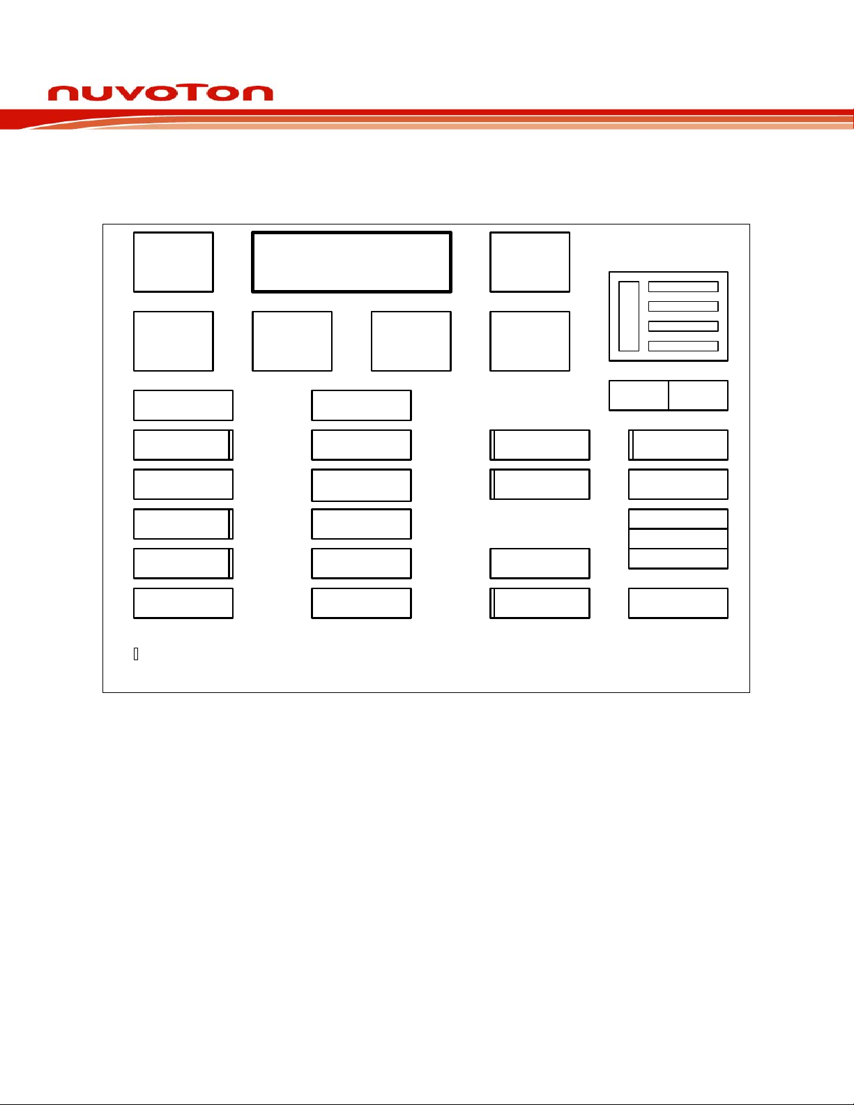
NUC120 Series DATA SHEET
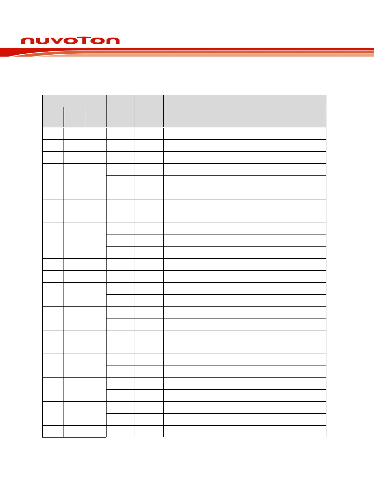
3 PARTS INFORMATION LIST AND PIN CONFIGURATION
3.1 Products Selection Guide
3.1.1 NUC120 Products Selection Guide
3.1.1.1 NUC120 series USB Line Selection Guide (Medium Density)
Part number Flash SRAM
NUC120LE3AN 128 KB 16 KB 2 1 2 1 1 4 1 8x12-bit 4x24-bit v v up to 31 LQFP48
NUC120LD3AN 64 KB 16 KB 2 1 2 1 1 4 1 8x12-bit 4x24-bit v v up to 31 LQFP48
NUC120RE3AN 128 KB 16 KB 2 2 2 1 1 6 2 8x12-bit 4x24-bit v v up to 45 LQFP64
NUC120RD3AN 64 KB 16 KB 2 2 2 1 1 6 2 8x12-bit 4x24-bit v v up to 45 LQFP64
NUC120VE3AN 128 KB 16 KB 3 4 2 1 1 8 2 8x12-bit 4x24-bit v v up to 76 LQFP100
NUC120VD3AN 64 KB 16 KB 3 4 2 1 1 8 2 8x12-bit 4x24-bit v v up to 76 LQFP100
NUC120VD2AN 64 KB 8 KB 3 4 2 1 1 8 2 8x12-bit 4x24-bit v v up to 76 LQFP100
UART
Connectivity
SPI/SSI
I2C USB
I2S PWM Comp. ADC Timer RTC
ISP
ICP
I/O Package
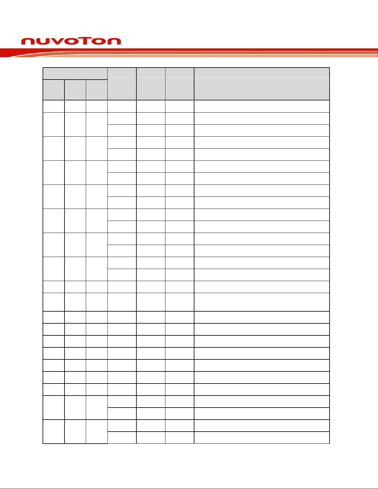
3.1.1.2 NUC120 series USB Line Selection Guide (Low Density)
※The following parts support one-channel PDMA
Part number Flash SRAM
NUC120LD2AN 64 KB 8 KB 2 1 2 1 1 4 1 8x12-bit 4x24-bit v v up to 31 LQFP48
NUC120LD1AN 64 KB 4 KB 2 1 2 1 1 4 1 8X12-Bit 4x24-bit v v up to 31 LQFP48
UART
Connectivity
SPI/SSI
I2C USB
I2S PWM Comp. ADC Timer RTC
ISP
ICP
I/O Package
NUC120LC1AN 32 KB 4 KB 2 1 2 1 1 4 1 8X12-Bit 4x24-bit v v up to 31 LQFP48
NUC120RD2AN 64 KB 8 KB 2 2 2 1 1 4 2 8x12-bit 4x24-bit v v up to 45 LQFP64
NUC120RD1AN 64 KB 4 KB 2 2 2 1 1 4 2 8X12-Bit 4x24-bit v v up to 45 LQFP64
NUC120RC1AN 32 KB 4 KB 2 2 2 1 1 4 2 8X12-Bit 4x24-bit v v up to 45 LQFP64
Publication Release Date: May 31, 2010
- 10 - Revision V1.02
Page 11
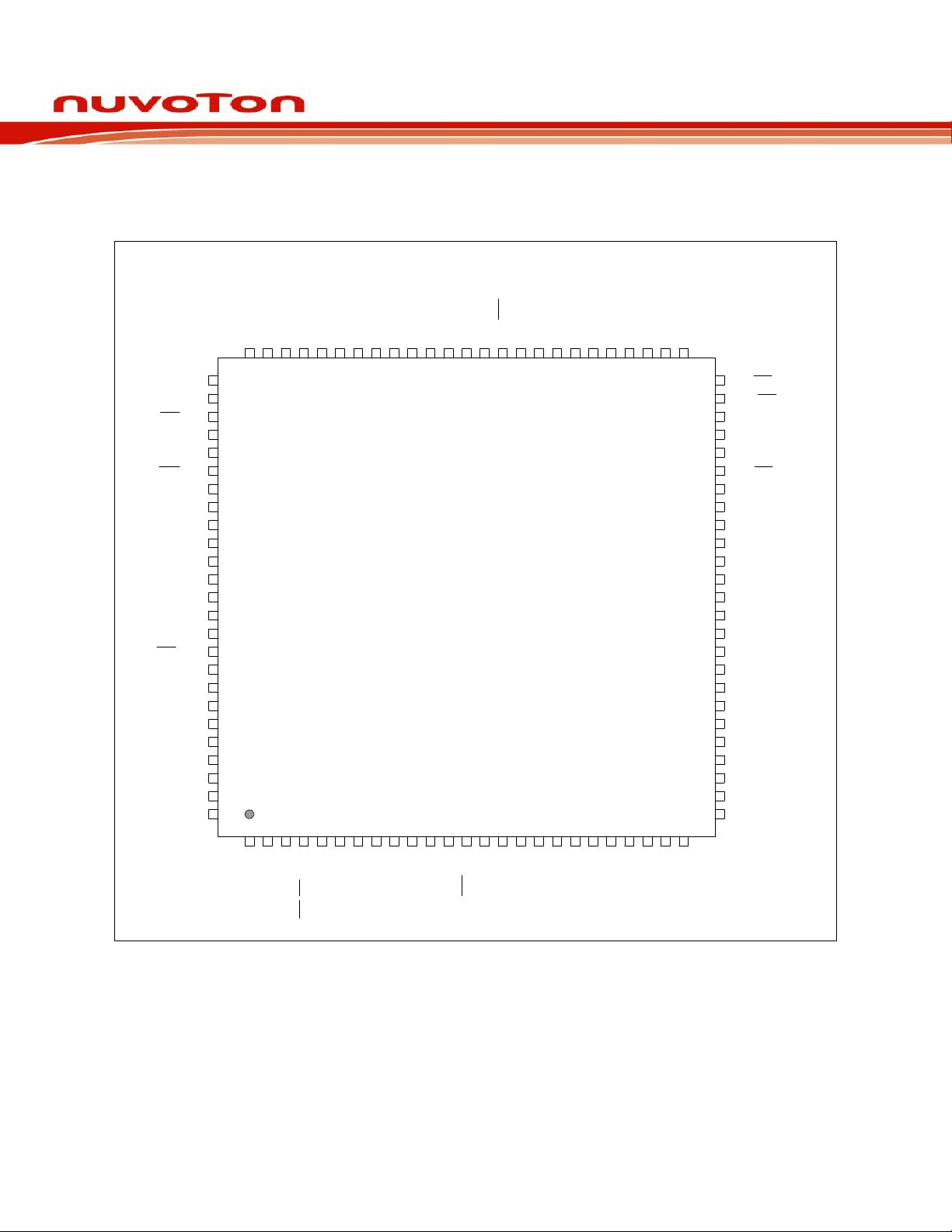
3.2 Pin Configuration
3.2.1 NUC120 LQFP 100 pin
PA.1/ADC1
PA.2/ADC2
PA.0/ADC0
5
AVSS
70
6
ADC5/PA.5
ADC6/PA.6
ADC7/SS21/PA.7
Vref
AVDD
SS20/PD.0
SPICLK2/PD.1
MISO20/PD.2
MOSI20/PD.3
MISO21/PD.4
MOSI21/PD.5
CPN0/PC.7
CPP0/PC.6
CPN1/PC.15
CPP1/PC.14
INT1/PB.15
XT1_Out
XT1_In
/RESET
VSS1
VDD1
PS2DAT
PS2CLK
PVSS
STADC/TM0/PB.8
PA.4/ADC4
7574737271
76
77
78
79
80
81
82
83
84
85
86
87
88
89
90
91
92
93
94
95
96
97
98
99
100
1
PA.3/ADC3
234
NUC120 Series DATA SHEET
VSS2
VDD2
ICE_DAT
ICE_CK
686766656469636261
7
8
9
PA.13/PWM1
PA.12/PWM0
LQFP 100-pin
101112131415161718192021222324
PC.9/SPICLK1
PC.10/MISO10
60
59
PC.11/MOSI10
PC.13/MOSI11
PC.12/MISO11
PE.0/PWM6
5857565554
PE.1/PWM7
PE.3
PE.2
535251
PE.4
PB.9/SS11/TM1
50
PB.10/SS01/TM2
49
PB.11/TM3/PWM4
48
PE.5/PWM5
47
PE.6
46
PC.0/SS00/I2SLRCLK
45
PC.1/SPICLK0/I2SBCLK
44
PC.2/MISO00/I2SDI
43
PC.3/MOSI00/I2SDO
42
PC.4/MISO01
41
PC.5/MOSI01
40
PD.15/TX2
39
PD.14/RX2
38
PD.7
37
PD.6
36
PB.3/CTS0
35
PB.2/RTS0
34
PB.1/TX0
33
PB.0/RX0
32
D+
31
D-
30
VDD33
29
VBUS
28
PE.7
27
PE.8
26
25
PC.8/SS10
PA.15/PWM3/I2SMCLK
PA.14/PWM2
VSS
X32I
PE.15
PE.14
PE.13
SS31/INT0/PB.14
X32O
CPO1/PB.13
CLKO/CPO0/PB.12
I2C1SCL/PA.11
I2C1SDA/PA.10
SS30/PD.8
I2C0SCL/PA.9
SPICLK3/PD.9
I2C0SDA/PA. 8
MISO31/PD.12
MISO30/PD.10
MOSI30/PD.11
TX1/PB.5
RX1/PB.4
MOSI31/PD.13
LDO
VDD
CTS1/PB.7
RTS1/PB.6
Publication Release Date: May 31, 2010
- 11 - Revision V1.02
Page 12
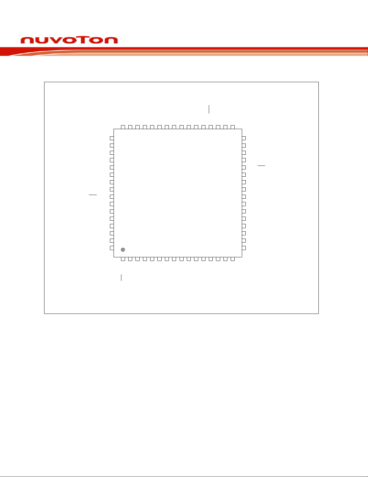
3.2.2 NUC120 LQFP 64 pin
PA.4/ADC4
PA.3/ADC3
PA.2/ADC2
PA.1/ADC1
PA.0/ADC0
NUC120 Series DATA SHEET
ICE_DAT
ICE_CK
AVSS
PA.13/PWM1
PA.12/PWM0
PA.14/PWM2
PC.9/SPICLK1
PC.8/SS10
PA.15/PWM3/I2SMCLK
PC.11/MOSI10
PC.10/MISO10
46
ADC5/PA.5
ADC6/PA.6
ADC7/PA.7
AVDD
CPN0/PC.7
CPP0/PC.6
CPN1/PC.15
CPP1/PC.14
INT1/PB.15
XT1_Out
XT1_In
/RESET
VSS1
VDD1
PVSS
STADC/TM0/PB.8
48
47
49
50
51
52
53
54
55
56
57
58
59
60
61
62
63
64
1
2
INT0/PB.14
CPO1/PB.13
45
3
4
X32O
CLKO/CPO0/PB.12
4443424140
LQFP 64-pin
5
6
7
8
9
X32I
I2C0SCL/PA.9
I2C1SCL/PA.11
I2C0SDA/PA.8
I2C1SDA/PA.10
39
10
RX1/PB.4
Note:
1. PWM4 and PWM5 are only supported in medium density version.
3736353433
38
11
1213141516
TX1/PB.5
CTS1/PB.7
RTS1/PB.6
32
PB.9/TM1
31
PB.10/TM2
30
PB.11/TM3/PWM4
29
PE.5/PWM5
28
PC.0/SS00/I2SLRCLK
27
PC.1/SPICLK0/I2SBCLK
26
PC.2/MISO00/I2SDI
25
PC.3/MOSI00/I2SDO
24
PB.3/CTS0
23
PB.2/RTS0
22
PB.1/TX0
21
PB.0/RX0
D+
20
19
D-
18
VDD33
17
VBUS
VSS
LDO
VDD
*1
*1
Publication Release Date: May 31, 2010
- 12 - Revision V1.02
Page 13
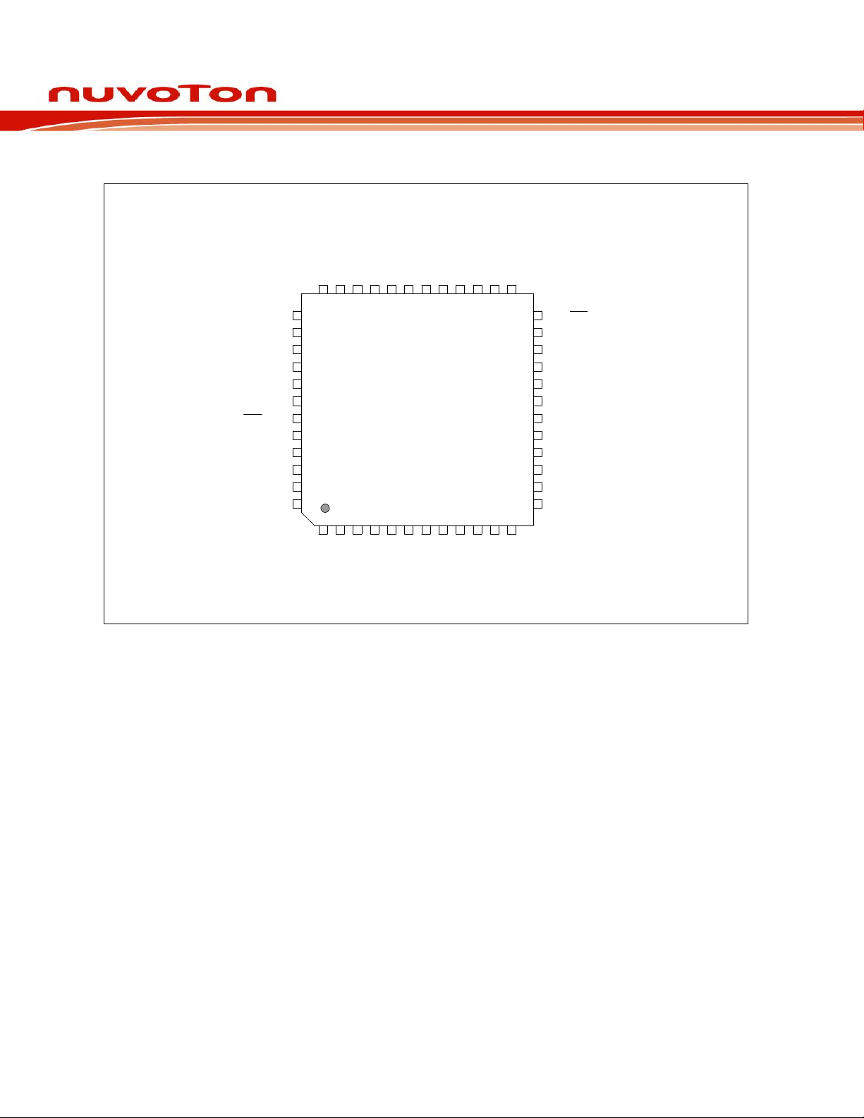
3.2.3 NUC120 LQFP 48 pin
PA.4/ADC4
PA.3/ADC3
PA.2/ADC2
NUC120 Series DATA SHEET
PA.1/ADC1
PA.0/ADC0
ICE_DAT
ICE_CK
AVSS
PA.13/PWM1
PA.12/PWM0
PA.15/PWM3/I2SMCLK
PA.14/PWM2
ADC5/PA.5
ADC6/PA.6
ADC7/PA.7
AVDD
CPN0/PC.7
CPP0/PC.6
INT1/PB.15
XT1_Out
XT1_In
/RESET
PVSS
STADC/TM0/PB.8
32363029282726
34
353133
37
38
39
40
41
42
43
44
45
46
47
48
1
CLKO/CPO0/PB.12
LQFP 48-pin
2
3
4
X32I
X32O
I2C1SCL/PA.11
I2C1SDA/PA.10
6
I2C0SCL/PA.9
7
I2C0SDA/PA.8
8
RX1/PB.4
9
TX1/PB.5
10511
LDO
VDD
25
24
PC.0/SS00/I2SLRCLK
23
PC.1/SPICLK0/I2SBCLK
22
PC.2/MISO00/I2SDI
21
PC.3/MOSI00/I2SDO
PB.3/CTS0
20
19
PB.2/RTS0
PB.1/TX0
18
17
PB.0/RX0
16
D+
15
D-
14
VDD33
13
VBUS
12
VSS
Publication Release Date: May 31, 2010
- 13 - Revision V1.02
Page 14
3.3 Pin Description
3.3.1 NUC120 Pin Description
Pin No.
LQFP
100
LQFP
64
LQFP
Pin Name Pin Type Description
48
NUC120 Series DATA SHEET
1 PE.15
2 PE.14
3 PE.13
PB.14
4 1
5 2
6 3 1
7 4 2 X32O
8 5 3 X32I
9 6 4
/INT0
/SPISS31
PB.13
CPO1
PB.12
CPO0
CLKO
PA.11
I2C1SCL
I/O
I/O
I/O
I/O
I
I/O
I/O
O
I/O
O
O
I
O
I/O
I/O
General purpose input/output digital pin
General purpose input/output digital pin
General purpose input/output digital pin
General purpose input/output digital pin
/INT0: External interrupt1 input pin
/SPISS31: SPI3 2
General purpose input/output digital pin
Comparator1 output pin
General purpose input/output digital pin
Comparator0 output pin
Frequency Divider output pin
32.768 kHz crystal output pin
32.768 kHz crystal input pin
General purpose input/output digital pin
I2C1SCL: I2C1 clock pin
nd
slave select pin
10 7 5
PA.10
I2C1SDA
PA.9
11 8 6
I2C0SCL
PA.8
12 9 7
I2C0SDA
PD.8
13
/SPISS30
PD.9
14
SPICLK3
15 PD.10
I/O
I/O
I/O
I/O
I/O
I/O
I/O
I/O
I/O
I/O
I/O
General purpose input/output digital pin
I2C1SDA: I2C1 data input/output pin
General purpose input/output digital pin
I2C0SCL: I2C0 clock pin
General purpose input/output digital pin
I2C0SDA: I2C0 data input/output pin
General purpose input/output digital pin
/SPISS30: SPI3 slave select pin
General purpose input/output digital pin
SPICLK3: SPI3 serial clock pin
General purpose input/output digital pin
Publication Release Date: May 31, 2010
- 14 - Revision V1.02
Page 15
LQFP
100
Pin No.
LQFP
64
LQFP
48
NUC120 Series DATA SHEET
Pin Name Pin Type Description
MISO30
PD.11
16
MOSI30
PD.12
17
MISO31
PD.13
18
MOSI31
PB.4
19 10 8
RX1
PB.5
20 11 9
TX1
PB.6
21 12
RTS1
PB.7
22 13
CTS1
I
I/O
O
I/O
I
I/O
O
I/O
I
I/O
O
I/O
I/O
MISO30: SPI3 MISO (Master In, Slave Out) pin
General purpose input/output digital pin
MOSI30: SPI3 MOSI (Master Out, Slave In) pin
General purpose input/output digital pin
nd
MISO31: SPI3 2
General purpose input/output digital pin
MOSI31: SPI3 2
General purpose input/output digital pin
RX1: Data Receiver input pin for UART1
General purpose input/output digital pin
TX1: Data transmitter output pin for UART1
General purpose input/output digital pin
RTS1: Request to Send output pin for UART1
General purpose input/output digital pin
CTS1: Clear to Send input pin for UART1
MISO (Master In, Slave Out) pin
nd
MOSI (Master Out, Slave In) pin
23 14 10 LDO
24 15 11 VDD
25 16 12 VSS
26 PE.8
27 PE.7
28 17 13 VBUS
29 18 14 VDD33
30 19 15 D-
31 20 16 D+
PB.0
32 21 17
RX0
PB.1
33 22 18
TX0
P
P
P
I/O
I/O
USB
USB
USB
USB
I/O
I
I/O
O
LDO output pin
Power supply for I/O ports and LDO source for
internal PLL and digital function
Ground
General purpose input/output digital pin
General purpose input/output digital pin
POWER SUPPLY: From USB Host or HUB.
Internal Power Regulator Output 3.3V Decoupling Pin
USB Differential Signal D-
USB Differential Signal D+
General purpose input/output digital pin
RX0: Data Receiver input pin for UART0
General purpose input/output digital pin
TX0: Data transmitter output pin for UART0
Publication Release Date: May 31, 2010
- 15 - Revision V1.02
Page 16
LQFP
100
Pin No.
LQFP
64
LQFP
48
NUC120 Series DATA SHEET
Pin Name Pin Type Description
34 23
35 24
36 19 PD.6
37 20 PD.7
38 PD.14
39 PD.15
40
41
42 25 21
PB.2
RTS0
PB.3
CTS0
PC.5
MOSI01
PC.4
MISO01
PC.3
MOSI00
I2SDO
I/O
I/O
I/O
I/O
I/O
I/O
I/O
O
I/O
I
I/O
O
O
General purpose input/output digital pin
RTS0: Request to Send output pin for UART0
General purpose input/output digital pin
CTS0: Clear to Send input pin for UART0
General purpose input/output digital pin
General purpose input/output digital pin
General purpose input/output digital pin
General purpose input/output digital pin
General purpose input/output digital pin
nd
MOSI01: SPI0 2
General purpose input/output digital pin
MISO01: SPI0 2
General purpose input/output digital pin
MOSI00: SPI0 MOSI (Master Out, Slave In) pin
I2SDO: I2S data output
MOSI (Master Out, Slave In) pin
nd
MISO (Master In, Slave Out) pin
PC.2
43 26 22
44 27 23
45 28 24
46 PE.6
47 29
MISO00
I2SDI
PC.1
SPICLK0
I2SBCLK
PC.0
/SPISS00
I2SLRCLK
PE.5
PWM5
PB.11
TM3
I/O
I
I
I/O
I/O
I/O
I/O
I/O
I/O
I/O
I/O
O
I/O
O
General purpose input/output digital pin
MISO00: SPI0 MISO (Master In, Slave Out) pin
I2SDI: I2S data input
General purpose input/output digital pin
SPICLK0: SPI0 serial clock pin
I2SBCLK: I2S bit clock pin
General purpose input/output digital pin
/SPISS00: SPI0 slave select pin
I2SLRCLK: I2S left right channel clock
General purpose input/output digital pin
General purpose input/output digital pin
PWM5: PWM output
General purpose input/output digital pin 48 30
TM3: Timer3 external counter input
Publication Release Date: May 31, 2010
- 16 - Revision V1.02
Page 17

LQFP
100
Pin No.
LQFP
64
LQFP
48
NUC120 Series DATA SHEET
Pin Name Pin Type Description
PWM4
PB.10
31
49
TM2
/SPISS01
PB.9
32
50
TM1
/SPISS11
51 PE.4
52 PE.3
53 PE.2
PE.1
54
PWM7
PE.0
55
PWM6
PC.13
56
MOSI11
O
I/O
O
I/O
I/O
O
I/O
I/O
I/O
I/O
I/O
O
I/O
O
I/O
O
PWM4: PWM output
General purpose input/output digital pin
TM2: Timer2 external counter input
/SPISS01: SPI0 2
nd
slave select pin
General purpose input/output digital pin
TM1: Timer1 external counter input
/SPISS11: SPI1 2
nd
slave select pin
General purpose input/output digital pin
General purpose input/output digital pin
General purpose input/output digital pin
General purpose input/output digital pin
PWM7: PWM output
General purpose input/output digital pin
PWM6: PWM output
General purpose input/output digital pin
nd
MOSI11: SPI1 2
MOSI (Master Out, Slave In) pin
57
PC.12
MISO11
PC.11
58 33
MOSI10
PC.10
59 34
MISO10
PC.9
60 35
SPICLK1
PC.8
61 36
/SPISS10
PA.15
62 37 25
PWM3
I2SMCLK
I/O
I
I/O
O
I/O
I
I/O
I/O
I/O
I/O
I/O
O
O
General purpose input/output digital pin
nd
MISO11: SPI1 2
MISO (Master In, Slave Out) pin
General purpose input/output digital pin
MOSI10: SPI1 MOSI (Master Out, Slave In) pin
General purpose input/output digital pin
MISO10: SPI1 MISO (Master In, Slave Out) pin
General purpose input/output digital pin
SPICLK1: SPI1 serial clock pin
General purpose input/output digital pin
/SPISS10: SPI1 slave select pin
General purpose input/output digital pin
PWM3: PWM output pin
I2SMCLK: I2S master clock output pin
Publication Release Date: May 31, 2010
- 17 - Revision V1.02
Page 18

LQFP
100
Pin No.
LQFP
64
LQFP
48
NUC120 Series DATA SHEET
Pin Name Pin Type Description
63 38 26
PA.14
PWM2
PA.13
64 39 27
PWM1
PA.12
65 40 28
PWM0
66 41 29 ICE_DAT
67 42 30 ICE_CLK
68 VDD2
69 31 VSS2
70 43 AVSS
PA.0
71 44 32
ADC0
PA.1
72 45 33
ADC1
I/O
O
I/O
O
I/O
O
I/O
I
P
P
AP
I/O
AI
I/O
AI
General purpose input/output digital pin
PWM2: PWM output
General purpose input/output digital pin
PWM1: PWM output
General purpose input/output digital pin
PWM0: PWM output
Serial Wired Debugger Data pin
Serial Wired Debugger Clock pin
Power supply for I/O ports and LDO source for
internal PLL and digital circuit
Ground
Ground Pin for analog circuit
General purpose input/output digital pin
ADC0: ADC analog input
General purpose input/output digital pin
ADC1: ADC analog input
73 46 34
74 47 35
75 48 36
76 49 37
77 50 38
78 51 39
PA.2
ADC2
PA.3
ADC3
PA.4
ADC4
PA.5
ADC5
PA.6
ADC6
PA.7
ADC7
/SPISS21
I/O
AI
I/O
AI
I/O
AI
I/O
AI
I/O
AI
I/O
AI
I/O
General purpose input/output digital pin
ADC2: ADC analog input
General purpose input/output digital pin
ADC3: ADC analog input
General purpose input/output digital pin
ADC4: ADC analog input
General purpose input/output digital pin
ADC5: ADC analog input
General purpose input/output digital pin
ADC6: ADC analog input
General purpose input/output digital pin
ADC7: ADC analog input
/SPISS21: SPI2 2
nd
slave select pin
Publication Release Date: May 31, 2010
- 18 - Revision V1.02
Page 19

LQFP
100
Pin No.
LQFP
64
LQFP
48
NUC120 Series DATA SHEET
Pin Name Pin Type Description
79 Vref
80 52 40 AVDD
PD.0
81
/SPISS20
PD.1
82
SPICLK2
PD.2
83
MISO20
PD.3
84
MOSI20
PD.4
85
MISO21
PD.5
86
MOSI21
PC.7
87 53 41
CPN0
AP
AP
I/O
I/O
I/O
I/O
I/O
I
I/O
O
I/O
I
I/O
O
I/O
I
Voltage reference input for ADC
Power supply for internal analog circuit
General purpose input/output digital pin
/SPISS20: SPI2 slave select pin
General purpose input/output digital pin
SPICLK2: SPI2 serial clock pin
General purpose input/output digital pin
MISO20: SPI2 MISO (Master In, Slave Out) pin
General purpose input/output digital pin
MOSI20: SPI2 MOSI (Master Out, Slave In) pin
General purpose input/output digital pin
nd
MISO21: SPI2 2
General purpose input/output digital pin
MOSI21: SPI2 2
General purpose input/output digital pin
CPN0: Comparator0 Negative input pin
MISO (Master In, Slave Out) pin
nd
MOSI (Master Out, Slave In) pin
88 54 42
PC.6
CPP0
PC.15
89 55
CPN1
PC.14
90 56
CPP1
PB.15
91 57 43
/INT1
92 58 44 XT1_OUT
93 59 45 XT1_IN
94 60 46 /RESET
95 61 VSS1
I/O
I
I/O
I
I/O
I
I/O
I
O
I
I
P
General purpose input/output digital pin
CPP0: Comparator0 Positive input pin
General purpose input/output digital pin
CPN1: Comparator1 Negative input pin
General purpose input/output digital pin
CPP1: Comparator1 Positive input pin
General purpose input/output digital pin
/INT1: External interrupt0 input pin
Crystal output pin
Crystal input pin
External reset input: Low active, set this pin low reset
MCU to initial state. With internal pull-up.
Ground
Publication Release Date: May 31, 2010
- 19 - Revision V1.02
Page 20
LQFP
100
Pin No.
LQFP
64
LQFP
48
NUC120 Series DATA SHEET
Pin Name Pin Type Description
96 62 VDD1
97 PS2DAT
98 PS2CLK
99 63 47 PVSS
PB.8
100 64 48
Note:
1. Pin Type I=Digital Input, O=Digital Output; AI=Analog Input; P=Power Pin; AP=Analog Power
STADC
TM0
P
I/O
I/O
I/O
I/O
I
O
Power supply for I/O ports and LDO source for
internal PLL and digital circuit
PS2 Data pin
PS2 clock pin
PLL Ground
General purpose input/output digital pin
STADC: ADC external trigger input.
TM0: Timer0 external counter input
Publication Release Date: May 31, 2010
- 20 - Revision V1.02
Page 21
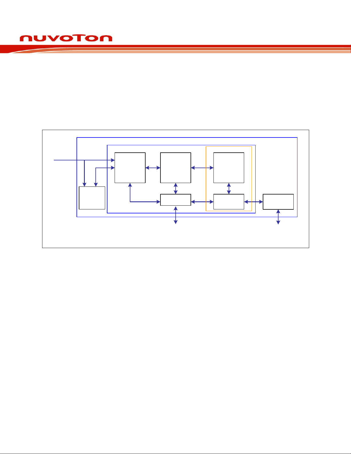
4 BLOCK DIAGRAM
4.1 NUC120 Block Diagram
NUC120 Series DATA SHEET
FLASH
128KB
ISP 4KB
PS2
SPI 2/3
I2C 1 -1M
UART 1 -115K
UART 2 -115K
I2S
Peripherals with PDMA
Cortex-M0
SRAM
16KB
50MHz
RTC
WDG
Timer 0/1/
Timer 2/3
PWM 4~7
I2C 0 -1M
GPIO
A,B,C,D,E
PDMA
CLK_CTL
SPI 0/1
UART 0 -3M
PWM 0~3
USB-FS
512BRAM
P
L
L
LDO
12-bit ADC
Analog
Comparator
Brown-out
USBPHY
10 kHz
32 KHz
22 MHz
12 MHz
2.5V~
5.5V
POR
LVR
Figure 4-1 NUC120 Block Diagram
Publication Release Date: May 31, 2010
- 21 - Revision V1.02
Page 22
NUC120 Series DATA SHEET
5 FUNCTIONAL DESCRIPTION
5.1 ARM® Cortex™-M0 core
The Cortex™-M0 processor is a configurable, multistage, 32-bit RISC processor. It has an AMBA
AHB-Lite interface and includes an NVIC component. It also has optional hardware debug
functionality. The processor can execute Thumb code and is compatible with other Cortex-M profile
processor.
Figure 5-1 shows the functional blocks of processor.
Cortex-M0 components
DebugCortex-M0 processor
Interrupts
Nested
Vectored
Interrupt
Controller
(NVIC)
Cortex-M0
Processor
core
Breakpoint
and
Watchpoint
unit
Wakeup
Interrupt
Controller
(WIC)
Bus matrix
AHB-Lite interface
Debugger
interface
Debug
Access Port
(DAP)
Serial Wire or
JTAG debug port
Figure 5-1 Functional Block Diagram
The implemented device provides:
• A low gate count processor that features:
– The ARMv6-M Thumb® instruction set.
– Thumb-2 technology.
– ARMv6-M compliant 24-bit SysTick timer.
– A 32-bit hardware multiplier.
– The system interface supports little-endian data accesses.
– The ability to have deterministic, fixed-latency, interrupt handling.
– Load/store-multiples and multicycle-multiplies that can be abandoned and restarted to facilitate
rapid interrupt handling.
– C Application Binary Interface compliant exception model.
This is the ARMv6-M, C Application Binary Interface(C-ABI) compliant exception model that
enables the use of pure C functions as interrupt handlers.
– Low power sleep-mode entry using Wait For Interrupt(WFI), Wait For Even(WFE) instructions,
or the return from interrupt sleep-on-exit feature.
• NVIC that features:
– 32 external interrupt inputs, each with four levels of priority.
– Dedicated non-Maskable Interrupt (NMI) input.
- 22 - Revision V1.02
Publication Release Date: May 31, 2010
Page 23

NUC120 Series DATA SHEET
– Support for both level-sensitive and pulse-sensitive interrupt lines
– Wake-up Interrupt Controller (WIC), providing ultra-low power sleep mode support.
• Debug support
– Four hardware breakpoints.
– Two watchpoints.
– Program Counter Sampling Register (PCSR) for non-intrusive code profiling.
– Single step and vector catch capabilities.
• Bus interfaces:
– Single 32-bit AMBA-3 AHB-Lite system interface that provides simple integration to all system
peripherals and memory.
– Single 32-bit slave port that supports the DAP (Debug Access Port).
Publication Release Date: May 31, 2010
- 23 - Revision V1.02
Page 24

NUC120 Series DATA SHEET
5.2 System Manager
5.2.1 Overview
The following functions are included in system manager section
y System Memory Map
y System Timer (SysTick)
y Nested Vectored Interrupt Controller (NVIC)
y System management registers for product ID
y System management registers for chip and module functional reset and multi-function pin control
y Brown-Out and chip miscellaneous Control Register
y Combined peripheral interrupt source identify
5.2.2 System Reset
The system reset includes one of the list below event occurs. For these reset event flags can be read
by RSTRC register.
y The Power-On Reset
y The low level on the /RESET pin
y Watchdog Time Out Reset
y Low Voltage Reset
y Brown-Out-Detected Reset
y Coretex-M0 MCU Reset
y PMU Reset
Publication Release Date: May 31, 2010
- 24 - Revision V1.02
Page 25

NUC120 Series DATA SHEET
5.2.3 System Timer (SysTick)
The Cortex-M0 includes an integrated system timer, SysTick. SysTick provides a simple, 24-bit
clear-on-write, decrementing, wrap-on-zero counter with a flexible control mechanism. The counter
can be used in several different ways, for example:
y An RTOS tick timer which fires at a programmable rate (for example 100Hz) and invokes a
SysTick routine.
y A high speed alarm timer using Core clock.
y A variable rate alarm or signal timer – the duration range dependent on the reference clock used
and the dynamic range of the counter.
y A simple counter. Software can use this to measure time to completion and time used.
y An internal clock source control based on missing/meeting durations. The COUNTFLAG bit-field
in the control and status register can be used to determine if an action completed within a set
duration, as part of a dynamic clock management control loop.
When enabled, the timer will count down from the value in the SysTick Current Value Register
(SYST_CVR) to zero, reload (wrap) to the value in the SysTick Reload Value Register (SYST_RVR)
on the next clock edge, then decrement on subsequent clocks. When the counter transitions to zero,
the COUNTFLAG status bit is set. The COUNTFLAG bit clears on reads.
The SYST_CVR value is UNKNOWN on reset. Software should write to the register to clear it to zero
before enabling the feature. This ensures the timer will count from the SYST_RVR value rather than
an arbitrary value when it is enabled.
If the SYST_RVR is zero, the timer will be maintained with a current value of zero after it is reloaded
with this value. This mechanism can be used to disable the feature independently from the timer
enable bit.
For more detailed information, please refer to the documents “ARM® Cortex™-M0 Technical
Reference Manual” and “ARM® v6-M Architecture Reference Manual”.
Publication Release Date: May 31, 2010
- 25 - Revision V1.02
Page 26

NUC120 Series DATA SHEET
5.2.4 Nested Vectored Interrupt Controller (NVIC)
Cortex-M0 provides an interrupt controller as an integral part of the exception mode, named as
“Nested Vectored Interrupt Controller (NVIC)”. It is closely coupled to the processor kernel and
provides following features:
y Nested and Vectored interrupt support
y Automatic processor state saving and restoration
y Dynamic priority changing
y Reduced and deterministic interrupt latency
The NVIC prioritizes and handles all supported exceptions. All exceptions are handled in “Handler
Mode”. This NVIC architecture supports 32 (IRQ[31:0]) discrete interrupts with 4 levels of priority. All of
the interrupts and most of the system exceptions can be configured to different priority levels. When
an interrupt occurs, the NVIC will compare the priority of the new interrupt to the current running one’s
priority. If the priority of the new interrupt is higher than the current one, the new interrupt handler will
override the current handler.
When any interrupts is accepted, the starting address of the interrupt service routine (ISR) is fetched
from a vector table in memory. There is no need to determine which interrupt is accepted and branch
to the starting address of the correlated ISR by software. While the starting address is fetched, NVIC
will also automatically save processor state including the registers “PC, PSR, LR, R0~R3, R12” to the
stack. At the end of the ISR, the NVIC will restore the mentioned registers from stack and resume the
normal execution. Thus it will take less and deterministic time to process the interrupt request.
The NVIC supports “Tail Chaining” which handles back-to-back interrupts efficiently without the
overhead of states saving and restoration and therefore reduces delay time in switching to pending
ISR at the end of current ISR. The NVIC also supports “Late Arrival” which improves the efficiency of
concurrent ISRs. When a higher priority interrupt request occurs before the current ISR starts to
execute (at the stage of state saving and starting address fetching), the NVIC will give priority to the
higher one without delay penalty. Thus it advances the real-time capability.
For more detailed information, please refer to the documents “ARM® Cortex™-M0 Technical
Reference Manual” and “ARM® v6-M Architecture Reference Manual”.
5.2.4.1 Exception Model and System Interrupt Map
The following table lists the exception model supported by NUC1xx serials. Software can set four
levels of priority on some of these exceptions as well as on all interrupts. The highest userconfigurable priority is denoted as “0” and the lowest priority is denoted as “3”. The default priority of
all the user-configurable interrupts is “0”. Note that priority “0” is treated as the fourth priority on the
system, after three system exceptions “Reset”, “NMI” and “Hard Fault”.
Publication Release Date: May 31, 2010
- 26 - Revision V1.02
Page 27

Table 5-1 Exception Model
NUC120 Series DATA SHEET
EExxcceeppttiioonn NNaammee
Reset
NMI
Hard Fault
Reserved
SVCall
Reserved
PendSV
SysTick
Interrupt (IRQ0 ~ IRQ31)
Table 5-2 System Interrupt Map
Vector
Number
Interrupt Number
(Bit in Interrupt
Registers)
VVeeccttoorr NNuummbbeerr
1
2
3
4 ~ 10
11
12 ~ 13
14
15
16 ~ 47
Interrupt
Name
Source IP Interrupt description
PPrriioorriittyy
-3
-2
-1
Reserved
Configurable
Reserved
Configurable
Configurable
Configurable
0 ~ 15 -
16 0
17 1
18 2
19 3
20 4
21 5
22 6
23 7
24 8
-
BOD_OUT
WDT_INT
EINT0
EINT1
GPAB_INT
GPCDE_INT
PWMA_INT
PWMB_INT
TMR0_INT
- System exceptions
Brown-Out Brownout low voltage detected interrupt
WDT Watch Dog Timer interrupt
GPIO External signal interrupt from PB.14 pin
GPIO External signal interrupt from PB.15 pin
GPIO External signal interrupt from PA[15:0] / PB[13:0]
GPIO External interrupt from PC[15:0]/PD[15:0]/PE[15:0]
PWM0~3 PWM0, PWM1, PWM2 and PWM3 interrupt
PWM4~7 PWM4, PWM5, PWM6 and PWM7 interrupt
TMR0 Timer 0 interrupt
Publication Release Date: May 31, 2010
- 27 - Revision V1.02
Page 28

NUC120 Series DATA SHEET
25 9
26 10
27 11
28 12
29 13
30 14
31 15
32 16
33 17
34 18
35 19
36 20 Reserved Reserved Reserved
TMR1_INT
TMR2_INT
TMR3_INT
UART02_INT
UART1_INT
SPI0_INT
SPI1_INT
SPI2_INT
SPI3_INT
I2C0_INT
I2C1_INT
TMR1 Timer 1 interrupt
TMR2 Timer 2 interrupt
TMR3 Timer 3 interrupt
UART0/2 UART0 and UART2 interrupt
UART1 UART1 interrupt
SPI0 SPI0 interrupt
SPI1 SPI1 interrupt
SPI2 SPI2 interrupt
SPI3 SPI3 interrupt
I2C0 I2C0 interrupt
I2C1 I2C1 interrupt
37 21 Reserved Reserved Reserved
38 22 Reserved Reserved Reserved
39 23
40 24
41 25
42 26
43 27
44 28
45 29
46 30 Reserved Reserved Reserved
47 31
USB_INT
PS2_INT
ACMP_INT
PDMA_INT
I2S_INT
PWRWU_INT
ADC_INT
RTC_INT
USBD USB FS Device interrupt
PS2 PS2 interrupt
ACMP Analog Comparator-0 or Comaprator-1 interrupt
PDMA PDMA interrupt
I2S I2S interrupt
CLKC
ADC0/1 ADC interrupt
RTC Real time clock interrupt
Clock controller interrupt for chip wake up from
power-down state
Publication Release Date: May 31, 2010
- 28 - Revision V1.02
Page 29

NUC120 Series DATA SHEET
5.3 Clock Controller
The clock controller generates the clock sources for the whole chip, including all AMBA interface
modules and all peripheral clocks. The clock controller also implements the power control function with
the individually clock on or off control, clock source selection and a 4-bit clock divider next to clock
source selection. The chip will into power-down mode after set the Power-Down bit and then the CPU
Cortex-M0 execute the WFI or the WFE instruction. On the power down mode, the controller turns off
the external crystal and internal oscillator to reduce the power consumption to minimum.
5.3.1 Clock Generator
The clock generator consists of 5 sources which list below:
• One external 32kHz crystal
• One external 12 MHz crystal
• One programmable PLL FOUT(PLL source consists of 12M and 22M)
• One internal 22 MHz oscillator
• One internal 10 kHz oscillator
XTL32K_EN(PWRCON[1])
X32I
XTL32K
X32O
XTL12M_EN(PWRCON[0])
XT_IN
XTL12M
XT_OUT
OSC22M_EN(PWRCON[6])
OSC22M
OSC10K_EN(PWRCON[3])
OSC10K
12M
22M
10K
PLL_SRC(PLLCON[19])
1
0
PLL
32K
12M
PLL FOUT
22M
10K
Figure 5-2 Clock generator block diagram
Publication Release Date: May 31, 2010
- 29 - Revision V1.02
Page 30

NUC120 Series DATA SHEET
5.3.2 System Clock & SysTick Clock
The system clock has 5 clock sources which were generated from clock generator block. The clock
source switch depends on the register HCLK_S(CLKSEL0[2:0]). The block diagram lists below.
HCLK_S(CLKSEL0[2:0])
22M
10K
PLLFOUT
32K
12M
1xx
011
010
001
000
CPU in Power Down Mode
1/(HCLK_N+1)
HCLK_N(CLKDIV[3:0])
CPUCLK
HCLK
PCLK
CPU
AHB
APB
Figure 5-3 System Clock Block Diagram
The SysTick clock(STCLK) has 5 clock sources which were generated from clock generator block.
The clock source switch depends on the setting of the register STCLK_S(CLKSEL0[5:3]. The block
diagram lists below.
STCLK_S(CLKSEL0[5:3])
22M
HCLK
12M
32K
12M
1/2
1/2
1/2
1xx
011
010
001
000
STCLK
Figure 5-4 SysTick clock Control Block Diagram
Publication Release Date: May 31, 2010
- 30 - Revision V1.02
Page 31

NUC120 Series DATA SHEET
5.3.3 Peripherals Clock
The peripherals clock had different clock source switch setting which depends on the different
peripheral. Please refer the CLKSEL1 & APBCLK register description.
5.3.4 Power down mode (Deep Sleep Mode) Clock
When enter into power down mode, some clock sources and peripherals clock and system clock will
be disable. Some clock sources and peripherals clock are still active in power down mode.
For theses clocks which still keep active list below:
z Clock Generator
Internal 10K oscillator clock
External 32K crystal clock
z Peripherals Clock (When these IP adopt 32K or 10K Hz as clock source)
Watch Dog Clock
RTC Clock
Timer 0/1/2/3 Clock
PWM Clock
ADC Clock
Publication Release Date: May 31, 2010
- 31 - Revision V1.02
Page 32

NUC120 Series DATA SHEET
5.3.5 Frequency Divider Output
This device is equipped a power-of-2 frequency divider which is composed by16 chained divide-by-2
shift registers. One of the 16 shift register outputs selected by a sixteen to one multiplexer is reflected
to GPIOB.12. Therefore there are 16 options of power-of-2 divided clocks with the frequency from
/21 to Fin/216 where Fin is input clock frequency to the clock divider.
F
in
The output formula is F
= Fin/2
out
output frequency and N is the 4-bit value in FREQDIV.FSEL[3:0].
When FREQDIV.FDIV_EN[4] is set to high, the rising transition will reset the chained counter and
starts it counting. When FREQDIV.FDIV_EN[4] is written with a zero, the chained counter continuously
runs till divided clock reaches low state and stay in low state.
(N+1)
, where F
is the input clock frequency, F
in
CLKSEL2.FRQDIV_S[3:2]
APBCLK.FRQDIV_EN[6]
is the clock divider
out
FRQDIV_CLK
22M
HCLK
32K
12M
FREQDIV.FDIV_EN[4]
0 to 1
Reset Clock
Divider
divide-by-2 counter
1/2 …...1/221/2
11
10
01
00
FRQDIV_CLK
Figure 5-5 Clock Source of Frequency Divider
16 chained
3
1/2151/2
16
000
001
:
16 to 1
:
MUX
110
111
FREQDIV.FSEL[3:0]
GPIOB_DOUT[12]
& ALT_MPF.PB12_CLKO=1
PB.12/CPO0/
1
0
GPIOB_MFP[12]
CLKO
Figure 5-6 Block Diagram of Frequency Divider
Publication Release Date: May 31, 2010
- 32 - Revision V1.02
Page 33

NUC120 Series DATA SHEET
5.4 USB Device Controller
5.4.1 Overview
NUC1XX series contain one set of USB 2.0 full-speed device controller and transceiver. It is compliant
with USB 2.0 full speed device specification and support control/bulk/interrupt/isochronous transfer
types.
In this device controller, it contains two main interfaces: the AHB bus and USB bus which comes from
the USB PHY transceiver. For the AHB bus, only the slave interface is implemented and the CPU will
program control registers through it. There are 512 bytes internal SRAM as data buffer in this
controller. For IN or OUT transfer, it is necessary to write data to SRAM or read data from SRAM
through the AHB slave interface or SIE. Users need to set the effective starting address of SRAM for
each endpoint buffer through “buffer segmentation register (BUFSEGx)”.
This device controller contains 6 configurable endpoints. Each endpoint needs to be configured
properly in advance for its attribution (IN, OUT or ISO state) & endpoint number. The transmit length in
each endpoint is defined in maximum payload register (MXPLDx). Note that most handshakes
between Host and Device are handled by hardware. Any USB event will cause an interrupt, and users
just need to check the related event flags in interrupt event flag register (EVF) to acknowledge what
kind of events occurring and store the required data into buffer, which is then sent to host by
hardware.
A software-disable function is also available for this USB device, which simulates the disconnection of
this device from the host.
5.4.2 Features
This Universal Serial Bus (USB) performs a serial interface with a single connector type for attaching
all USB peripherals to the host system. Following is the feature list of this USB.
y Compliant with USB 2.0 Full-Speed specification.
y Provide 1 interrupt vector with 4 different interrupt events.
y Support Control/Bulk/Interrupt/Isochronous transfer type.
y Support suspend function when no bus activity showing for 3 ms.
y Provide 6 endpoints for configurable Control/Bulk/Interrupt/Isochronous transfer types and
maximum 512 bytes buffer size.
y Provide remote wakeup capability.
Publication Release Date: May 31, 2010
- 33 - Revision V1.02
Page 34

5.4.3 Block Diagram
USB_DPUSB_DM
PAD
NUC120 Series DATA SHEET
CLK_GEN
AIC
D+
D-
FLODET
RXDP
RXDM
S0
S1
flo_debounce
SIE
dpll
Endpoints
UIE
Wakeup
BUFFER
CONTROL
int
SFR
SRAM
512
BYTES
Transceiver
APB WRAPPER
USB_TOP
APB Bus
Figure 5-7 USB Block Diagram
Publication Release Date: May 31, 2010
- 34 - Revision V1.02
Page 35

NUC120 Series DATA SHEET
5.5 General Purpose I/O
5.5.1 Overview and Features
Up to 80 General Purpose I/O pins can be shared with other function pins; it depends on the chip
configuration. These 80 pins are arranged in 5 ports named with GPIOA, GPIOB, GPIOC, GPIOD and
GPIOE. Each port equips maximum 16 pins. Each one of the 80 pins is independent and has the
corresponding register bits to control the pin mode function and data.
The I/O type of each of I/O pins can be independently software configured as input, output, open-drain
or quasi-bidirectional mode. The all pins of I/O type stay in quasi-bidirectional mode and port data
register GPIOx_DOUT[15:0] resets to 0x000_FFFF. Each I/O pin equips a very weakly individual pullup resistor which is about 110KΩ~300KΩ for V
5.5.1.1 Input Mode Explanation
Set GPIOx_PMD (PMDn[1:0]) to 00b the GPIOx port [n] pin is in Input mode and the I/O pin is in tri-state
(high impedance) without output drive capability.
corresponding port pins.
is from 5.0V to 2.5V.
DD
The GPIOx_PIN value reflects the status of the
5.5.1.2 Output Mode Explanation
Set GPIOx_PMD (PMDn[1:0]) to 01b the GPIOx port [n] pin is in Output mode and the I/O pin supports
digital output function with source/sink current capability. The bit value in the corresponding bit [n] of
GPIO_DOUT is driven on the pin.
VDD
P
Port Pin
Port Latch
Data
Input Data
N
Figure 5-8 Push-Pull Output
Publication Release Date: May 31, 2010
- 35 - Revision V1.02
Page 36

NUC120 Series DATA SHEET
5.5.1.3 Open-Drain Mode Explanation
Set GPIOx_PMD (PMDn[1:0]) to 10b the GPIOx port [n] pin is in Open-Drain mode and the I/O pin
supports digital output function but only with sink current capability, an additional pull-up resister is
needed for driving high state. If the bit value in the corresponding bit [n] of GPIOx_DOUT is “0”, the pin
drive a “low” output on the pin. If the bit value in the corresponding bit [n] of GPIOx_DOUT is “1”, the
pin output drives high that is controlled by the internal pull-up resistor or the external pull high resistor.
Port Pin
Port Latch
Data
Input Data
N
Figure 5-9 Open-Drain Output
5.5.1.4 Quasi-bidirectional Mode Explanation
Set GPIOx_PMD (PMDn[1:0]) to 11b the GPIOx port [n] pin is in Quasi-bidirectional mode and the I/O
pin supports digital output and input function at the same time but the source current is only up to
hundreds uA. Before the digital input function is performed the corresponding bit in GPIOx_DOUT
must be set to 1. The quasi-bidirectional output is common on the 80C51 and most of its derivatives. If
the bit value in the corresponding bit [n] of GPIOx_DOUT is “0”, the pin drive a “low” output on the pin.
If the bit value in the corresponding bit [n] of GPIOx_DOUT is “1”, the pin will check the pin value. If
pin value is high, no action takes. If pin state is low, then pin will drive strong high with 2 clock cycles
on the pin and then disable the strong output drive and then the pin status is control by internal pull-up
resistor. Note that the source current capability in quasi-bidirectional mode is only about 200uA to
30uA for VDD is form 5.0V to 2.5V
VDD
Port Latch
Data
2 CPU
Clock Delay
Input Data
PP P
N
Figure 5-10 Quasi-bidirectional I/O Mode
- 36 - Revision V1.02
Strong
Very
Weak
Weak
Publication Release Date: May 31, 2010
Port Pin
Page 37

NUC120 Series DATA SHEET
5.6 I2C Serial Interface Controller (Master/Slave)
5.6.1 Introduction
I2C is a two-wire, bi-directional serial bus that provides a simple and efficient method of data
exchange between devices. The I2C standard is a true multi-master bus including collision detection
and arbitration that prevents data corruption if two or more masters attempt to control the bus
simultaneously. Serial, 8-bit oriented bi-directional data transfers can be made up to 100kbit/s in
Standard-mode, up to 400kbit/s in the Fast-mode, or up to 1.0 Mbit/s in the Fast-mode Plus.
Data is transferred between a Master and a Slave synchronously to SCL on the SDA line on a byteby-byte basis. Each data byte is 8 bits long. There is one SCL clock pulse for each data bit with the
MSB being transmitted first. An acknowledge bit follows each transferred byte. Each bit is sampled
during the high period of SCL; therefore, the SDA line may be changed only during the low period of
SCL and must be held stable during the high period of SCL. A transition on the SDA line while SCL is
high is interpreted as a command (START or STOP). Please refer to Figure 5-11 for more detail I2C
BUS Timing.
Repeated
START
t
SU;STA
t
SU;STO
STOP
SDA
SCL
STOP
t
BUF
START
t
HD;STA
t
LOW
t
HIGH
t
HD;DAT
t
r
t
f
t
SU;DAT
Figure 5-11 I2C Bus Timing
The device’s on-chip I2C logic provides the serial interface that meets the I2C bus standard mode
specification. The I2C port handles byte transfers autonomously. To enable this port, the bit ENS1 in
I2CON should be set to '1'. The I2C H/W interfaces to the I2C bus via two pins: SDA (Px.y, serial data
line) and SCL (Px.y, serial clock line). Pull up resistor is needed for Pin Px.y and Px.y for I2C
operation as these are open drain pins. When the I/O pins are used as I2C port, user must set the pins
to logic high in advance.
Publication Release Date: May 31, 2010
- 37 - Revision V1.02
Page 38

NUC120 Series DATA SHEET
5.6.2 Features
The I2C bus uses two wires (SDA and SCL) to transfer information between devices connected to the
bus. The main features of the bus are:
y Master/Slave up to 1Mbit/s
y Bidirectional data transfer between masters and slaves
y Multi-master bus (no central master)
y Arbitration between simultaneously transmitting masters without corruption of serial data on the
bus
y Serial clock synchronization allows devices with different bit rates to communicate vian one serial
bus
y Serial clock synchronization can be used as a handshake mechanism to suspend and resume
serial transfer
y Built-in a 14-bit time-out counter will request the I2C interrupt if the I2C bus hangs up and timer-
out counter overflows.
y External pull-up are needed for high output
y Programmable clocks allow versatile rate control
y Supports 7-bit addressing mode
y I2C-bus controllers support multiple address recognition ( Four slave address with mask option)
Publication Release Date: May 31, 2010
- 38 - Revision V1.02
Page 39

NUC120 Series DATA SHEET
5.7 PWM Generator and Capture Timer
5.7.1 Introduction
This chip has 4 sets of PWM Generators which can be configured as 8 independent PWM outputs,
PWM0~PWM7, or as 4 complementary PWM pairs, (PWM0, PWM1), (PWM2, PWM3), (PWM4,
PWM5) and (PWM6, PWM7) with 4 programmable dead-zone generators. Each PWM Generator has
one 8-bit prescaler, one clock divider providing 5 divided frequencies (1, 1/2, 1/4, 1/8, 1/16), two PWM
Timers including two clock selectors, two 16-bit PWM down-counters for PWM period control, two 16bit comparators for PWM duty control and one dead-zone generator. The 4 sets of PWM Generators
provide eight independent PWM interrupt flags which are set by hardware when the corresponding
PWM period down counter reaches zero. Each PWM interrupt source with its corresponding enable bit
can cause CPU to request PWM interrupt. The PWM generators can be configured as one-shot mode
to produce only one PWM cycle signal or continuous mode to output PWM waveform continuously.
When PCR.DZEN01 is set, PWM0 and PWM1 perform complementary PWM paired function; the
paired PWM timing, period, duty and dead-time are determined by PWM0 timer and Dead-zone
generator 0. Similarly, the complementary PWM pairs of (PWM2, PWM3), (PWM4, PWM5) and
(PWM6, PWM7) are controlled by PWM2, PWM4 and PWM6 timers and Dead-zone generator 2, 4
and 6, respectively.
To prevent PWM driving output pin with unsteady waveform, the 16-bit period down counter and 16-bit
comparator are implemented with double buffer. When user writes data to counter/comparator buffer
registers the updated value will be load into the 16-bit down counter/ comparator at the time down
counter reaching zero. The double buffering feature avoids glitch at PWM outputs.
When the 16-bit period down counter reaches zero, the interrupt request is generated. If PWM-timer is
set as continuous mode, when the down counter reaches zero, it is reloaded with PWM Counter
Register (CNRx) automatically then start decreasing, repeatedly. If the PWM-timer is set as one-shot
mode, the down counter will stop and generate one interrupt request when it reaches zero.
The value of PWM counter comparator is used for pulse width modulation. The counter control logic
changes the output level when down-counter value matches the value of compare register.
The alternate feature of the PWM-timer is digital input Capture function. If Capture function is enabled
the PWM output pin is switched as capture input mode. The Capture0 and PWM0 share one timer
which is included in PWM 0; and the Capture1 and PWM1 share PWM1 timer, and etc. Therefore user
must setup the PWM-timer before enable Capture feature. After capture feature is enabled, the
capture always latched PWM-counter to Capture Rising Latch Register (CRLR) when input channel
has a rising transition and latched PWM-counter to Capture Falling Latch Register (CFLR) when input
channel has a falling transition. Capture channel 0 interrupt is programmable by setting
CCR0.CRL_IE0[1] (Rising latch Interrupt enable) and CCR0.CFL_IE0[2]] (Falling latch Interrupt
enable) to decide the condition of interrupt occur. Capture channel 1 has the same feature by setting
CCR0.CRL_IE1[17] and CCR0.CFL_IE1[18]. And capture channel 2 to channel 7 have the same
feature by setting the corresponding control bits in CCR1 to CCR3. Whenever Capture issues Interrupt
0/1/2/3, the PWM counter 0/1/2/3 will be reload at this moment.
Publication Release Date: May 31, 2010
- 39 - Revision V1.02
Page 40

NUC120 Series DATA SHEET
5.7.2 Features
5.7.2.1 PWM function features:
y Four PWM Generators, each one supports one 8-bit prescaler, one clock divider, PWM-timer,
one dead-zone generator and two PWM outputs.
y Up to 8 PWM channels or 4 PWM paired channels.
y Up to 16 bits resolution.
y PWM Interrupt request synchronous with PWM period.
y Single-shot or Continuous mode PWM.
y Four Dead-Zone generators
5.7.2.2 Capture Function Features:
y Timing control logic shared with PWM Generators.
y 8 Capture input channels.
y Each channel support one rising latch register (CRLR), one falling latch register (CFLR) and
Capture interrupt flag (CAPIFx)
Publication Release Date: May 31, 2010
- 40 - Revision V1.02
Page 41

NUC120 Series DATA SHEET
5.8 Real Time Clock (RTC)
5.8.1 Overview
Real Time Clock (RTC) unit provides user the real time and calendar message. The clock source of
RTC is from an external 32.768KHz crystal connected at pins X32I and X32O or from an external
32.768KHz oscillator output fed at pin X32I. The RTC unit provides the time message(second, minute,
hour) in Time Loading Register (TLR) as well as calendar message(day, month, year) in Calendar
Loading Register (CLR). The data message is expressed in BCD format. This unit offers alarm
function that user can preset the alarm time in Time Alarm Register (TAR) and alarm calendar in
Calendar Alarm Register (CAR).
The RTC unit supports periodic Time Tick and Alarm Match interrupts. The periodic interrupt has 8
period options 1/128, 1/64, 1/32, 1/16, 1/8, 1/4, 1/2 and 1 second which are selected by
TTR(TTR[2:0]). When RTC counter in TLR and CLR is equal to alarm setting time registers TAR and
CAR, the alarm interrupt flag (RIIR.AIF) is set and the alarm interrupt is requested if the alarm interrupt
is enabled (RIER.AIER=1). The RTC Time Tick and Alarm Match can cause CPU wakeup from sleep
or power-down mode if Wakeup CPU function is enabled(TWKE(TTR[3])=1).
5.8.2 RTC Features
y There is a time counter (second, minute, hour) and calendar counter (day, month, year) for user
to check the time.
y Alarm register (second, minute, hour, day, month, year).
y 12-hour or 24-hour mode is selectable.
y Leap year compensation automatically.
y Day of week counter.
y Frequency compensate register (FCR).
y All time and calendar message is expressed in BCD code.
y Support periodic time tick interrupt with 8 period options 1/128, 1/64, 1/32, 1/16, 1/8, 1/4, 1/2 and
1 second.
y Support RTC Time Tick and Alarm Match interrupt
y Support wake up CPU from sleep or power-down mode.
Publication Release Date: May 31, 2010
- 41 - Revision V1.02
Page 42

NUC120 Series DATA SHEET
5.9 Serial Peripheral Interface (SPI) Controller
5.9.1 Overview
The Serial Peripheral Interface (SPI) is a synchronous serial data communication protocol which
operates in full duplex mode. Devices communicate in master/slave mode with 4-wire bi-direction
interface. NUC1XX series contain up to four sets of SPI controller performing a serial-to-parallel
conversion on data received from a peripheral device, and a parallel-to-serial conversion on data
transmitted to a peripheral device. Each set of SPI controller can be set as a master that can drive up
to 2 external peripheral slave devices; it also can be set as a slave controlled by an off-chip master
device.
5.9.2 Features
y Four sets of SPI controller
y Support master or slave operation
y Support 1 and 2-bit serial data IN/OUT
y Configurable data length of transfer word up to 32 bits
y Variable output serial clock frequency in master mode
y Provide burst mode operation, transmit/receive can be executed up to two times in one transfer
y MSB or LSB first data transfer
y 2 slave/device select lines when it is set as the master mode, and 1 slave/device select line
when it is set as slave mode
y Fully static synchronous design with one clock domain
y Byte Suspend Sleep Mode
y Support two programmable serial output clock frequency.
Publication Release Date: May 31, 2010
- 42 - Revision V1.02
Page 43

NUC120 Series DATA SHEET
5.10 Timer Controller
5.10.1 General Timer Controller
The timer module includes four channels, TIMER0~TIMER3 (TIMER0 and TIMER1 are at APB1 and
TIMER2 and TIMER3 are at APB2), which allow user to easily implement a counting scheme or timing
control for applications. The timer can perform functions like frequency measurement, event counting,
interval measurement, clock generation, delay timing, and so on. The timer can generates an interrupt
signal upon timeout, or provide the current value of count during operation.
5.10.2 Features
y Independent clock source for each channel (TMR0_CLK, TMR1_CLK, TMR2_CLK, TMR3_CLK).
y Time out period = (Period of timer clock input) * (8-bit Prescale + 1) * (24-bit TCMP)
y Maximum counting cycle time = (1 / 25 MHz) * (2^8) * (2^24), if TCLK = 25 MHz.
y Internal 24-bit up counter is readable through TDR (Timer Data Register).
Publication Release Date: May 31, 2010
- 43 - Revision V1.02
Page 44

NUC120 Series DATA SHEET
5.11 Watchdog Timer
The purpose of Watchdog Timer is to perform a system reset after the software running into a
problem. This prevents system from hanging for an infinite period of time. Besides, this Watchdog
Timer supports the function to wakeup CPU from power-down mode. The watchdog timer includes a
19-bit free running counter with programmable time-out intervals.
Setting WTE (WDTCR[7]) enables the watchdog timer and the WDT counter starts counting up. When
the counter reaches the selected time-out interval, Watchdog timer interrupt flag WTIF will be set
immediately to request a WDT interrupt if the watchdog timer interrupt enable bit WTIE is set, in the
meanwhile, a specified delay time follows the time-out event. User must set WTR (WDTCR[0])
(Watchdog timer reset) high to reset the 19-bit WDT counter to avoid CPU from Watchdog timer reset
before the delay time expires. WTR bit is auto cleared by hardware after WDT counter is reset. There
are eight time-out intervals with specific delay time which are selected by Watchdog timer interval
select bits WTIS (WDTCR[10:8]). If the WDT counter has not been cleared after the specific delay
time expires, the watchdog timer will set Watchdog Timer Reset Flag (WTRF) high and reset CPU.
This reset will last 64 WDT clocks then CPU restarts executing program from reset vector (0x0000
0000). WTRF will not be cleared by Watchdog reset. User may poll WTFR by software to recognize
the reset source.
Table 5-3 Watchdog Timeout Interval Selection
WTIS
000 24 WDT_CLK (24 + 1024) WDT_CLK 69.33 us 31.7 ms
001 26 WDT_CLK (26 + 1024) WDT_CLK 72.53 us 33.2 ms
010 28 WDT_CLK (28 + 1024) WDT_CLK 85.33 us 39 ms
011 210 WDT_CLK (210 + 1024) WDT_CLK 170.67 us 64 ms
100 212 WDT_CLK (212 + 1024) WDT_CLK 426.67 us 160 ms
101 214 WDT_CLK (214 + 1024) WDT_CLK 1.45 ms 544 ms
110 216 WDT_CLK (216 + 1024) WDT_CLK 5.55 ms 2080 ms
111 218 WDT_CLK (218 + 1024) WDT_CLK 21.93 ms 8224 ms
Interrupt
Timeout
Watchdog Reset
Timeout
WTR Timeout Interval
(WDT_CLK=12 MHz)
WTR Timeout Interval
(WDT_CLK=32kHz)
Publication Release Date: May 31, 2010
- 44 - Revision V1.02
Page 45

NUC120 Series DATA SHEET
5.12 UART Interface Controller
This MCU provides three channels of Universal Asynchronous Receiver/Transmitters (UART). UART0
supports High Speed UART and UART1~2 perform Normal Speed UARTs, besides, only UART0 and
UART1 support flow control function.
5.12.1 Overview
The Universal Asynchronous Receiver/Transmitter (UART) performs a serial-to-parallel conversion on
data received from the peripheral, and a parallel-to-serial conversion on data transmitted from the
CPU. The UART controller also supports LIN master mode function and IrDA SIR Function. Each
UART channel supports seven types of interrupts including transmitter FIFO empty
interrupt(INT_THRE), receiver threshold level reaching interrupt (INT_RDA), line status interrupt
(overrun error or parity error or framing error or break interrupt) (INT_RLS), time out interrupt
(INT_Tout), MODEM/Wakeup status interrupt (INT_Modem), Buffer error interrupt (INT_Buf_Err) and
LIN receiver break field detected interrupt.
The UART0 are built-in with a 64-byte transmitter FIFO (TX_FIFO) and a 64-byte receiver FIFO
(RX_FIFO) that reduces the number of interrupts presented to the CPU and the UART1~2 are
equipped 16-byte transmitter FIFO (TX_FIFO) and 16-byte receiver FIFO (RX_FIFO). The CPU can
read the status of the UART at any time during the operation. The reported status information includes
the type and condition of the transfer operations being performed by the UART, as well as 4 error
conditions (parity error, overrun error, framing error and break interrupt) probably occur while receiving
data. The UART includes a programmable baud rate generator that is capable of dividing crystal clock
input by divisors to produce the clock that transmitter and receiver need. The baud rate equation is
Baud Rate = UART_CLK / M * [BRD + 2], where M and BRD are defined in Baud Rate Divider
Register (UA_BAUD). Table 5-4 lists the equations in the various conditions.
The UART0 and UART1 controllers support auto-flow control function that uses two low-level signals,
/CTS (clear-to-send) and /RTS (request-to-send), to control the flow of data transfer between the
UART and external devices (ex: Modem). When auto-flow is enabled, the UART is not allowed to
receive data until the UART asserts /RTS to external device. When the number of bytes in the Rx
FIFO equals the value of RTS_Tri_Lev(UA_FCR[19:16]), the /RTS is de-asserted. The UART sends
data out when UART controller detects /CTS is asserted from external device. If a validly asserted
/CTS is not detected the UART controller will not send data out.
The UART controllers also provides Serial IrDA (SIR, Serial Infrared) function (User must set
IrDA_EN(UA_FUN_SEL[1])to enable IrDA function). The SIR specification defines a short-range
infrared asynchronous serial transmission mode with one start bit, 8 data bits, and 1 stop bit. The
maximum data rate is 115.2 Kbps (half duplex). The IrDA SIR block contains an IrDA SIR Protocol
encoder/decoder. The IrDA SIR protocol is half-duplex only. So it cannot transmit and receive data at
the same time. The IrDA SIR physical layer specifies a minimum 10ms transfer delay between
transmission and reception. This delay feature must be implemented by software.
The alternate function of UART controllers is LIN(Local Interconnect Network) function. The LIN mode
is selected by setting the LIN_EN bit in UA_FUN_SEL register. In LIN mode, one start bit and 8-bit
data format with 1-bit stop bit are required in accordance with the LIN standard.
Table 5-4 UART Baud Rate Equation
DIV_X_EN DIV_X_ONE Divider X BRD Baud rate equation
Disable 0 B A UART_CLK / [16 * (A+2)]
Enable 0 B A UART_CLK / [(B+1) * (A+2)] , B must >= 8
Enable 1 B A UART_CLK / (A+2), A must >=3
Publication Release Date: May 31, 2010
- 45 - Revision V1.02
Page 46

NUC120 Series DATA SHEET
5.12.2 Features of UART controller
z The UART control supports three channels, UART0, UART1 and UART2.
z UART0/UART1/UART2 supports 64/16/16 bytes entry FIFO for received and transmitted data
payloads.
z Auto flow control/flow control function (/CTS, /RTS) are supported in UART0 and UART1.
z Individual programmable baud-rate generator for each channel.
z Fully programmable serial-interface characteristics:
5-, 6-, 7-, or 8-bit character.
Even, odd, or no-parity bit generation and detection.
1-, 1&1/2, or 2-stop bit generation.
Baud rate generation.
False start bit detection.
z Support IrDA SIR Function.
z Support LIN master mode.
z
Publication Release Date: May 31, 2010
- 46 - Revision V1.02
Page 47

NUC120 Series DATA SHEET
5.13 PS2 Device Controller (PS2D)
5.13.1 Overview
PS/2 device controller provides basic timing control for PS/2 communication. All communication
between the device and the host is managed through the CLK and DATA pins. Unlike PS/2 keyboard
or mouse device controller, the received/transmit code needs to be translated as meaningful code by
firmware. The device controller generates the CLK signal after receiving a request to send, but host
has ultimate control over communication. DATA sent from the host to the device is read on the rising
edge and DATA sent from device to the host is change after rising edge. A 16 bytes FIFO is used to
reduce CPU intervention. S/w can select 1 to 16 bytes for a continuous transmission.
5.13.2 Features
y APB interface compatible
y Host communication inhibit and request to send detection
y Reception frame error detection
y Programmable 1 to 16 bytes transmit buffer to reduce CPU intervention
y Double buffer for data reception
y S/W override bus
Publication Release Date: May 31, 2010
- 47 - Revision V1.02
Page 48

NUC120 Series DATA SHEET
5.14 I2S Controller
5.14.1 Overview
The I2S controller consists of IIS protocol to interface with external audio CODEC. Two 8 word deep
FIFO for read path and write path respectively and is capable of handling 8 ~ 32 bit word sizes. DMA
controller handles the data movement between FIFO and memory.
5.14.2 Features
y APB interface compatible
y I2S can operate as either master or slave
y Capable of handling 8, 16, and 32 bit word sizes.
y Mono and stereo audio data supported.
y I2S and MSB justified data format supported.
y Two 8 word FIFO data buffers are provided, one for transmit and one for receive.
y Generates interrupt requests when buffer levels cross a programmable boundary.
y Two DMA requests, one for transmit and one for receive.
Publication Release Date: May 31, 2010
- 48 - Revision V1.02
Page 49

NUC120 Series DATA SHEET
5.15 Analog-to-Digital Converter (ADC)
5.15.1 Functional Description
NUC1XX series contain one 12-bit successive approximation analog-to-digital converters (SAR A/D
converter) with 8 input channels. The A/D converter supports three operation modes: single, singlecycle scan and continuous scan mode. There are two kinds of scan mode: continuous mode and
single cycle mode. The A/D converters can be started by software and external STADC/PB.8 pin.
Note that the analog input port pins must be configured as input type before ADC function is enabled.
5.15.2 Features
y Analog input voltage range: 0~Vref (Max to 5.0V).
y 12-bits resolution and 10-bits accuracy is guaranteed.
y Up to 8 single-end analog input channels or 4 differential analog input channels.
y Maximum ADC clock frequency is 16MHz.
y Up to 800kHz SPS conversion rate, conversion time is less than 1.25us.
y Three operating modes
- Single mode: A/D conversion is performed one time on a specified channel.
- Single-cycle scan mode: A/D conversion is performed one cycle on all specified channels
with the sequence from the lowest numbered channel to the highest numbered channel.
- Continuous scan mode: A/D converter continuously performs Single-cycle scan mode until
software stops A/D conversion.
y An A/D conversion can be started by
- Software write 1 to ADST bit
- External pin STADC
y Conversion results are held in data registers for each channel with valid and overrun indicators.
y Conversion result can be compared with specify value and user can select whether to generate
an interrupt when conversion result is equal to the compare register setting.
y Channel 7 supports 4 input sources: external analog voltage, internal fixed bandgap voltage,
internal temperature sensor output and analog ground.
y Support Self-calibration to minimum conversion error.
Publication Release Date: May 31, 2010
- 49 - Revision V1.02
Page 50

NUC120 Series DATA SHEET
5.16 Analog Comparator
5.16.1 Functional Description
NUC120 series contains two comparators. The comparators can be used in a number of different
configurations. The comparator output is a logical one when positive input greater than negative input,
otherwise the output is a zero. Each comparator can be configured to cause an interrupt when the
comparator output value changes.
Note that the analog input port pins must be configured as input type before Analog Comparator
function is enabled.
5.16.2 Features
z Analog input voltage range: 0~5.0V
z Software enabled with hysteresis function
z Two analog comparators with optional internal reference voltage input at negative end
z One comparator interrupt requested by either comparator
Publication Release Date: May 31, 2010
- 50 - Revision V1.02
Page 51

NUC120 Series DATA SHEET
5.17 PDMA Controller
5.17.1 Overview
The NUC120 contains a peripheral direct memory access (PDMA) controller that transfers data to and
from memory or transfer data to and from APB. The PDMA has nine channels of DMA (Peripheral-toMemory or Memory-to-Peripheral or Memory-to-Memory). For each PDMA channel (PDMA
CH0~CH8), there is one word buffer to do transfer buffer between the Peripherals APB IP and
Memory.
Software can stop the PDMA operation by disable PDMA [PDMACEN]. The CPU can recognize the
completion of a PDMA operation by software polling or when it receives an internal PDMA interrupt.
The NUC120 PDMA controller can increment source or destination address, fixed or wrap around
them as well.
5.17.2 Features
y AMBA AHB master/slave interface compatible, for data transfer and register read/write.
y PDMA support 32-bit source and destination addressing range address increment, fixed and
wrap around.
Publication Release Date: May 31, 2010
- 51 - Revision V1.02
Page 52

NUC120 Series DATA SHEET
6 FLASH MEMORY CONTROLLER (FMC)
6.1 Overview
NUC1XX series equips with 128/64/32K bytes on chip embedded Flash EEPROM for application
program memory (APROM) that can be updated through ISP/IAP procedure. In System Programming
(ISP) function enables user to update program memory when chip is soldered on PCB. After chip
power on Cortex-M0 CPU fetches code from APROM or LDROM decided by boot select (CBS) in
Config0. By the way, NUC1XX series also provide additional 4k bytes DATA Flash for user, to store
some application dependent data before chip power off, in 64/32k APROM model. For 128k bytes
device, the data flash is shared with original 128k program memory and its start address is
configurable and defined by user in Config1. The data flash size is defined by user depends on her
application request.
6.2 Features
y AHB interface compatible
y Run up to 50 MHz with zero wait state for discontinuous address read access
y 128/64/32KB application program memory (APROM)
y 4KB in system programming (ISP) loader program memory (LDROM)
y Configurable or fixed 4KB data flash with 512 bytes page erase unit
y Programmable data flash start address and memory size for 128K program memory
y In System Program (ISP)/In Application Program (IAP) to update on chip Flash EPROM
Publication Release Date: May 31, 2010
- 52 - Revision V1.02
Page 53

7 ELECTRICAL CHARACTERISTICS
7.1 Absolute Maximum Ratings
SYMBOL PARAMETER MIN MAX UNIT
NUC120 Series DATA SHEET
DC Power Supply
Input Voltage VIN VSS-0.3 VDD+0.3 V
Oscillator Frequency 1/t
Operating Temperature TA -40 +85
Storage Temperature TST -55 +150
Maximum Current into VDD - 120 mA
Maximum Current out of VSS 120 mA
Maximum Current sunk by a
I/O pin
Maximum Current sourced by
a I/O pin
Maximum Current sunk by
total I/O pins
Maximum Current sourced by
total I/O pins
Note: Exposure to conditions beyond those listed under absolute maximum ratings may adversely affects the lift and reliability of the device.
VDD−VSS
0 40 MHz
CLCL
35 mA
35 mA
100 mA
100 mA
-0.3 +7.0 V
°C
°C
Publication Release Date: May 31, 2010
- 53 - Revision V1.02
Page 54

NUC120 Series DATA SHEET
7.2 DC Electrical Characteristics
(VDD-VSS=3.3V, TA = 25°C, F
PARAMETER SYM.
Operation voltage VDD 2.5 5.5 V VDD =2.5V ~ 5.5V up to 50 MHz
Power Ground
= 50 MHz unless otherwise specified.)
OSC
SPECIFICATION
MIN. TYP. MAX.
V
AV
SS
SS
-0.3 V
UNI
T
TEST CONDITIONS
LDO Output Voltage
(bypass = 0)
LDO Output Voltage
(bypass = 0)
V
LDO
V
LDO
-10% 2.45 +10%
V VDD > 2.7V
-10% VDD +10% V VDD < 2.7V
Analog Operating Voltage AVDD 0 VDD V
Analog Reference Voltage Vref 0 AVDD V
VDD= 5.5V@50Mhz,
enable all IP and PLL, XTAL=12MHz
=5.5V@50Mhz,
V
DD
disable all IP and enable PLL,
XTAL=12MHz
= 3V@50Mhz,
V
DD
enable all IP and PLL, XTAL=12MHz
= 3V@50Mhz,
V
DD
disable all IP and enable PLL,
Operating Current
Normal Run Mode
@ 50Mhz
I
50 mA
DD1
I
33 mA
DD2
I
45 mA
DD3
27 mA
I
DD4
XTAL=12MHz
= 5.5V@12Mhz,
V
DD
I
22 mA
DD5
enable all IP and disable PLL,
XTAL=12MHz
= 5.5V@12Mhz,
V
DD
I
Operating Current
Normal Run Mode
@ 12Mhz
15 mA
DD6
I
20 mA
DD7
disable all IP and disable PLL,
XTAL=12MHz
= 3V@12Mhz,
V
DD
enable all IP and disable PLL,
XTAL=12MHz
= 3V@12Mhz,
V
DD
I
12 mA
DD8
disable all IP and disable PLL,
XTAL=12MHz
Publication Release Date: May 31, 2010
- 54 - Revision V1.02
Page 55

Operating Current
Normal Run Mode
@ 4Mhz
Operating Current
Idle Mode
@ 50Mhz
Operating Current
Idle Mode
@ 12Mhz
Operating Current
Idle Mode
@ 4Mhz
NUC120 Series DATA SHEET
I
5.8 mA
DD9
I
4.2 mA
DD10
I
5.1 mA
DD11
I
3.6 mA
DD12
I
35 mA
IDLE1
I
15 mA
IDLE2
I
34 mA
IDLE3
I
13 mA
IDLE4
I
14 mA
IDLE5
I
5 mA
IDLE6
I
12 mA
IDLE7
I
4 mA
IDLE8
I
3.4 mA
IDLE9
I
1.8 mA
IDLE10
I
2.8 mA
IDLE11
I
1.2 mA
IDLE12
= 5V@4Mhz,
V
DD
enable all IP and disable PLL,
XTAL=4MHz
= V@4Mhz,
V
DD
disable all IP and disable PLL,
XTAL=4MHz
V
= 3V@4Mhz,
DD
enable all IP and disable PLL,
XTAL=4MHz
= 3V@4Mhz,
V
DD
disable all IP and disable PLL,
XTAL=4MHz
VDD= 5.5V@50Mhz,
enable all IP and PLL, XTAL=12MHz
=5.5V@50Mhz,
V
DD
disable all IP and enable PLL,
XTAL=12MHz
= 3V@50Mhz,
V
DD
enable all IP and PLL, XTAL=12MHz
= 3V@50Mhz,
V
DD
disable all IP and enable PLL,
XTAL=12MHz
= 5.5V@12Mhz,
V
DD
enable all IP and disable PLL,
XTAL=12MHz
= 5.5V@12Mhz,
V
DD
disable all IP and disable PLL,
XTAL=12MHz
= 3V@12Mhz,
V
DD
enable all IP and disable PLL,
XTAL=12MHz
= 3V@12Mhz,
V
DD
disable all IP and disable PLL,
XTAL=12MHz
= 5V@4Mhz,
V
DD
enable all IP and disable PLL,
XTAL=4MHz
= V@4Mhz,
V
DD
disable all IP and disable PLL,
XTAL=4MHz
= 3V@4Mhz,
V
DD
enable all IP and disable PLL,
XTAL=4MHz
= 3V@4Mhz,
V
DD
disable all IP and disable PLL,
XTAL=4MHz
Publication Release Date: May 31, 2010
- 55 - Revision V1.02
Page 56

NUC120 Series DATA SHEET
Standby Current
Power-down Mode
(Deep Sleep Mode)
Input Current PA, PB, PC,
PD, PE
Input Current at /RESET
[1]
I
Input Leakage Current PA, PB,
PC, PD, PE
Logic 1 to 0 Transition Current
PA~PE (Quasi-bidiretional mode)
Input Low Voltage PA, PB, PC,
PD, PE (TTL input)
Input High Voltage PA, PB, PC,
PD, PE (TTL input)
Input Low Voltage XT1
Input High Voltage XT1
Input Low Voltage X32I
Input High Voltage X32O
[*2]
[*2]
V
[*2]
[*2]
V
Negative going threshold
(Schmitt input), /RST
Positive going threshold
(Schmitt input), /RST
I
23
PWD1
I
18
PWD2
I
28
PWD3
I
22
PWD4
I
-60 - +15
IN1
-55 -45 -30
IN2
I
-2 - +2
LK
[3]
I
-650 - -200
TL
V
IL1
V
IH1
V
IL3
IH3
V
IL4
IH4
V
ILS
V
IHS
-0.3 - 1.0 V
-0.3 - 0.6 V V
V
2.2 -
1.5 -
0 - 0.8 V V
0 - 0.4 V
3.5 -
2.4 -
0 - 0.8
0 - 0.4
3.5 -
2.4 -
DD
+0.2
V
DD
+0.2
V
DD
+0.2
V
DD
+0.2
V
DD
+0.2
V
DD
+0.2
-0.5 - 0.3V
V
0.7V
DD
-
DD
5
DD
+0.
VDD = 5.5V, RTC OFF, No load
μA
@ Disable BOV function
V
= 3.3V, RTC OFF, No load
μA
μA
μA
μA
μA
μA
μA
DD
@ Disable BOV function
V
= 5.5V, RTC run , No load
DD
@ Disable BOV function
V
= 3.3V, RTC run , No load
DD
@ Disable BOV function
VDD = 5.5V, VIN = 0V or VIN=V
VDD = 5.5V, V
= 0.45V
IN
VDD = 5.5V, 0<VIN<VDD
VDD = 5.5V, V
= 4.5V
DD
= 2.5V
DD
= 5.5V
V
DD
<2.0V
IN
V
=3.0V
V
DD
= 4.5V
DD
= 3.0V
DD
DD
DD
= 5.5V
= 3.0V
V V
V
V
V
DD
Internal /RST pin pull up resistor
R
Hysteresis voltage V
50 100 KΩ
RST
HY
0.2V
DD
Publication Release Date: May 31, 2010
- 56 - Revision V1.02
V
Page 57

NUC120 Series DATA SHEET
I
-300 -370 -450
SR11
Source Current PA, PB, PC, PD,
I
PE (Quasi-bidirectional Mode)
Source Current PA, PB, PC, PD,
PE (Push-pull Mode)
Sink Current PA, PB, PC, PD,
PE (Quasi-bidirectional and
Push-pull Mode)
Brownout voltage with
BOV_VL [1:0] =00b
Brownout voltage with
BOV_VL [1:0] =01b
Brownout voltage with
BOV_VL [1:0] =10b
Brownout voltage with
BOV_VL [1:0] =11b
-50 -70 -90
SR12
I
-40 -60 -80
SR12
I
-20 -24 -28 mA V
SR21
I
-4 -6 -8 mA VDD = 2.7V, VS = 2.2V
SR22
-3 -5 -7 mA VDD = 2.5V, VS = 2.0V
I
SR22
I
10 16 20 mA V
SK1
I
7 10 13 mA VDD = 2.7V, V
SK1
6 9 12 mA VDD = 2.5V, V
I
SK1
V
2.1 2.2 2.3 V
BO2.2
V
2.6 2.7 2.8 V
BO2.7
3.7 3.8 3.9 V
V
BO3.8
V
4.4 4.5 4.6 V
BO4.5
Hysteresis range of BOD voltage VBH 30 - 150 mV VDD = 2.5V~5.5V
Notes:
1. /RST pin is a Schmitt trigger input.
2. XTAL1 is a CMOS input.
3. Pins of P0, P1, P2, P3 and P4 can source a transition current when they are being externally driven from 1 t o 0. In the condit ion of V
maximum value when Vin approximates to 2V .
VDD = 4.5V, V
μA
VDD = 2.7V, VS = 2.2V
μA
VDD = 2.5V, VS = 2.0V
μA
= 4.5V, V
DD
= 4.5V, V
DD
= 2.4V
S
= 2.4V
S
= 0.45V
S
= 0.45V
S
= 0.45V
S
=5.5V, 5he transition current reaches its
DD
Publication Release Date: May 31, 2010
- 57 - Revision V1.02
Page 58

7.3 AC Electrical Characteristics
NUC120 Series DATA SHEET
t
CLCL
t
CLCH
t
CLCX
t
CHCL
t
CHCX
Note: Duty cycle is 50%.
PARAMETER SYMBOL MIN. TYP. MAX. UNITS CONDITION
Clock High Time
Clock Low Time
Clock Rise Time
Clock Fall Time
20 - - nS
t
CHCX
20 - - nS
t
CLCX
- - 10 nS
t
CLCH
- - 10 nS
t
CHCL
7.3.1 External XTAL1 Oscillator
PARAMETER CONDITION MIN. TYP. MAX. UNIT
Input clock frequency External crystal 4 12 24 MHz
Temperature - -40 - 85
℃
VDD - 2.5 5 5.5 V
Publication Release Date: May 31, 2010
- 58 - Revision V1.02
Page 59

7.3.1.1 Typical Crystal Application Circuits
CRYSTAL C1 C2 R
4MHz ~ 24 MHz without without without
C1
R
C2
NUC120 Series DATA SHEET
XTAL1
XTAL2
Figure 7-1 Typical Crystal Application Circuit
Publication Release Date: May 31, 2010
- 59 - Revision V1.02
Page 60

NUC120 Series DATA SHEET
7.3.2 External 32kHz XTAL Oscillator
PARAMETER CONDITION MIN. TYP. MAX. UNIT
Input clock frequency External crystal - 32.768 - kHz
Temperature - -40 - 85
VDD - 2.5 - 5.5 V
Operating current VDD = 5V - 5 - uA
℃
7.3.3 Internal 22.1184MHz Oscillator
PARAMETER CONDITION MIN. TYP. MAX. UNIT
Supply voltage
Center Frequency - - 22.1184 MHz
Calibrated Internal Oscillator
Frequency
Accuracy of Un-calibrated
Internal Oscillator
Frequency
Operating current VDD =5V - 500 - uA
[1]
- 2.5 - 5.5 V
+25°C; VDD =5V
-40°C~+85°C;
V
=2.5V~5.5V
DD
-40°C~+85°C;
V
=2.5V~5.5V
DD
-1 - +1 %
-3 - +3 %
-25 - +25 %
7.3.4 Internal 10kHz Oscillator
PARAMETER CONDITION MIN. TYP. MAX. UNIT
Supply voltage
Center Frequency - - 10 - kHz
Calibrated Internal Oscillator
Frequency
Operating current VDD =5V - 5 - uA
Notes:
1. Internal operation voltage comes form LDO.
[1]
- 2.5 - 5.5 V
+25°C; VDD =5V
-40°C~+85°C;
V
=2.5V~5.5V
DD
-30 - +30 %
-50 - +50 %
Publication Release Date: May 31, 2010
- 60 - Revision V1.02
Page 61

NUC120 Series DATA SHEET
7.4 Analog Characteristics
7.4.1 Specification of 12-bit SARADC
PARAMETER SYM. MIN. TYP. MAX. UNIT
Resolution - - - 12 Bit
Differential nonlinearity error DNL - ±3 - LSB
Integral nonlinearity error INL - ±4 - LSB
Offset error EO - ±1 10 LSB
Gain error (Transfer gain) EG - 1 1.005 -
Monotonic - Guaranteed -
ADC clock frequency FADC - - 20 MHz
Calibration time TCAL - 127 - Clock
Sample time TS - 7 - Clock
Conversion time TADC - 13 - Clock
Sample rate FS - - 800 Ksps
V
- 2.5 - V
Supply voltage
Supply current (Avg.)
Reference voltage VREF - VDDA - V
Reference current (Avg.) IREFP - 1 - mA
Input voltage range VIN 0 - VREF V
Capacitance CIN - 5 - pF
LDO
VADD 3 - 5.5 V
IDD - 0.5 - mA
IDDA - 1.5 - mA
Publication Release Date: May 31, 2010
- 61 - Revision V1.02
Page 62

NUC120 Series DATA SHEET
7.4.2 Specification of LDO & Power management
PARAMETER MIN TYP MAX UNIT NOTE
Input Voltage 2.7 5 5.5 V VDD input voltage
Output Voltage
(bypass=0)
Output Voltage
(bypass=1)
Temperature -40 25 85 oC
Quiescent Current
(PD=0, bypass=0)
Quiescent Current
(PD=1, bypass=0)
Quiescent Current
(PD=1, bypass=1)
Iload (PD=0) - - 100 mA
Iload (PD=1) - - 100 uA
Cbp - 1u - F Resr=1ohm
Cload - 250p - F
-10% 2.45 +10% V LDO output voltage
-10% Input
Voltage
- 100 - uA
- 5 - uA
- 5 - uA
+10% V Input Voltage < 2.7V
Note:
1. It is recommended that a 10uF or higher capacitor and a 100nF bypass capacitor are connected
between VDD and the closest VSS pin of the device.
2. For ensuring power stability, a 4.7uF or higher capacitor must be connected between LDO pin
and the closest VSS pin of the device. Also a 100nF bypass capacitor between LDO and VSS
help suppressing output noise.
Publication Release Date: May 31, 2010
- 62 - Revision V1.02
Page 63

7.4.3 Specification of Low Voltage Reset
PARAMETER CONDITION MIN. TYP. MAX. UNIT
NUC120 Series DATA SHEET
Operation voltage - 1.7
Quiescent current VDD5V=5.5V - - 5 uA
Temperature
Temperature=25° 1.7 2.0 2.3 V
Threshold voltage
Hysteresis - 0 0 0 V
Temperature=-40° - 2.4 - V
Temperature=85° - 1.6 - V
-
-40 25 85
-
5.5 V
7.4.4 Specification of Brownout Detector
PARAMETER CONDITION MIN. TYP. MAX. UNIT
Operation voltage - 2.5
Quiescent current AVDD=5.5V - - 125 μA
Temperature
-
-40 25 85
-
5.5 V
℃
℃
BOV_VL[1:0]=11 4.4 4.5 4.6 V
Brown-out voltage
Hysteresis
BOV_VL [1:0]=10 3.7 3.8 3.9 V
BOV_VL [1:0]=01 2.6 2.7 2.8 V
BOV_VL [1:0]=00 2.1 2.2 2.3 V
-
30m
-
150m V
7.4.5 Specification of Power-On Reset (5V)
PARAMETER CONDITION MIN. TYP. MAX. UNIT
Temperature - -40 25 85 ℃
Reset voltage V+ - 2 - V
Quiescent current Vin>reset voltage - 1 - nA
Publication Release Date: May 31, 2010
- 63 - Revision V1.02
Page 64

NUC120 Series DATA SHEET
7.4.6 Specification of Temperature Sensor
PARAMETER MIN TYP MAX UNIT CONDITIONS
Supply voltage
Temperature -40 - 125 ℃
Current consumption 6.4 - 10.5 uA
Gain -1.95 -2 -2.05 mV/℃
Offset 688 708 730 mV Temp=0 ℃
Notes:
1. Internal operation voltage comes form LDO.
[1]
2.5 - 5.5 V
7.4.7 Specification of Comparator
PARAMETER MIN. TYP. MAX. CONDITION
Temperature -40℃ 25 ℃ 85℃ -
VDD 2.4 3 5.5 -
VDD current - 20uA 40uA 20uA@VDD=3V
Input offset voltage - 5mV 15mV -
Output swing 0.1 - VDD-0.1 -
Input common mode
range
DC gain - 70dB - -
Propagation delay - 200ns - @VCM=1.2V & VDIFF=0.1V
Comparison voltage 10mV 20mV -
Hysteresis - ±10mV -
Wake up time - - 2us
0.1 - VDD-1.2 -
20mV@VCM=1V
50mV@VCM=0.1V
50mV@VCM=VDD-1.2
@10mV for non-hysteresis
One bit control
W/O & W. hysteresis
@VCM=0.4V ~ VDD-1.2V
@CINP=1.3V
CINN=1.2V
Publication Release Date: May 31, 2010
- 64 - Revision V1.02
Page 65

NUC120 Series DATA SHEET
7.4.8 Specification of USB PHY
7.4.8.1 USB DC Electrical Characteristics
SYMBOL PARAMETER CONDITIONS MIN. TYP MAX. UNIT
VIH Input high (driven) 2.0 V
VIL Input low 0.8 V
VDI Differential input sensitivity |PADP-PADM| 0.2 V
VCM Differential
common-mode range
VSE Single-ended receiver threshold 0.8 2.0 V
Receiver hysteresis 200
VOL Output low (driven) 0 0.3
VOH Output high (driven) 2.8 3.6
V
Output signal cross voltage 1.3 2.0
CRS
RPU Pull-up resistor 1.425 1.575
RPD Pull-down resistor 14.25 15.75
V
Termination Voltage for
TRM
Z
DRV
CIN Transceiver capacitance Pin to GND 20
*Driver output resistance doesn’t include series resistor resistance.
upstream port pull up (R
Driver output resistance Steady state drive* 10
PU
)
Includes VDI range 0.8 2.5 V
mV
kΩ
kΩ
3.0 3.6
Ω
pF
V
V
V
V
Publication Release Date: May 31, 2010
- 65 - Revision V1.02
Page 66

NUC120 Series DATA SHEET
7.4.8.2 USB Full-Speed Driver Electrical Characteristics
SYMBOL PARAMETER CONDITIONS MIN. TYP MAX. UNIT
TFR Rise Time CL=50p 4 20 ns
TFF Fall Time CL=50p 4 20 ns
T
Rise and fall time matching T
FRFF
FRFF=TFR/TFF
7.4.8.3 USB Power Dissipation
SYMBOL PARAMETER CONDITIONS MIN. TYP MAX. UNIT
90 111.11 %
I
VDDREG
(Full
Speed)
VDDD and VDDREG Supply Current
(Steady State)
Standby 50 uA
Input mode uA
Output mode
uA
Publication Release Date: May 31, 2010
- 66 - Revision V1.02
Page 67

NUC120 Series DATA SHEET
8 PACKAGE DIMENSIONS
8.1.1 100L LQFP (14x14x1.4 mm footprint 2.0mm)
H
D
D
7
51
A2
A
A1
7
H
E
E
100
1
e
θ
b
25
50
26
L1
L
c
Y
Controlling Dimension : Millimeters
Symbol
A
A1
A
b
c
D
E
e
H
H
L
L1
y
θ
Dimension in inch
Nom
Min
0.002
0.053
0.007
0.004
0.547
0.547
D
0.622
0.622
E
0.018
Max Max
0.063
0.057
0.055
0.011
0.009
0.006
0.008
0.551
0.556
0.551
0.556
0.020
0.638
0.630
0.638
0.630
0.030
0.024
0.039
0.004
Dimension in mm
Nom
Min
0.05
1.35
1.40
0.22
0.17
0.15
0.10
14.00
13.90
13.90
14.00 14.10
0.50
16.00
15.80
15.80
16.00
0.60
0.45
1.00
070
1.60
1.45
0.27
0.20
14.10
16.20
16.20
0.75
0.10
7
Publication Release Date: May 31, 2010
- 67 - Revision V1.02
Page 68

NUC120 Series DATA SHEET
8.1.2 64L LQFP (10x10x1.4mm footprint 2.0 mm )
Symbol
A
1
A
2
A
b
c
D
E
e
D
H
E
H
L
1
L
y
0
Dimension in inch
Nom
Min
0.002
0.053
0.007
0.008 0.20
0.004
0.393
0.393
0.020
0.018
0
Max Max
0.063
0.006
0.057
0.055
0.011
0.008
0.472
0.472
0.030
0.024
0.039
0.004
3.5
7
Dimension in mm
Nom
Min
0.05
1.35
1.40
0.17
0.09
10.00
10.00
0.50
12.00
12.00
0.60
0.45
1.00
0.10
3.5
0
1.60
0.15
1.45
0.27
0.20
0.75
7
Publication Release Date: May 31, 2010
- 68 - Revision V1.02
Page 69

NUC120 Series DATA SHEET
H
8.1.3 48L LQFP (7x7x1.4mm footprint 2.0mm)
D
D
36
25
A2
A
A1
H
E
E
SEATING PLANE
48
37
24
13
1
e
b
Y
Controlling dimension : Millimeters
Symbol
Dimension in inch Dimension in mm
Nom
Min
A
1
A
2
0.053
A
0.006
b
c
D
E
e
D
H
E
H
L
1
L
0.008
0.006 0.15
0.004
0.272
0.276
0.272
0.276
0.020
0.014
0.350
0.354
0.350
0.354
0.024
0.018
0.039
Y
0
12
Min
1.35
0.15
0.10
6.90
6.90
0.35
8.90
8.90
070
Nom
0.100.050.002 0.004 0.006 0.15
1.40
0.20
7.00
7.00
0.50
0.600.45
1.00
1.45
0.25
0.20
7.10
7.10
0.65
9.109.00
9.109.00
0.75
0.10
Max Max
0.0570.055
0.010
0.008
0.280
0.280
0.026
0.358
0.358
0.030
0.004
c
θ
L
L1
7
Publication Release Date: May 31, 2010
- 69 - Revision V1.02
Page 70

9 REVISION HISTORY
NUC120 Series DATA SHEET
VERSION DATE
V1.00
V1.01 April 9, 2010 Ch4 1. Modify the block diagram
V1.02 May 31, 2010 7.2 1. Add operation current of DC characteristics
March 1,
2010
PAGE/
CHAP.
- Preliminary version initial issued
DESCRIPTION
Publication Release Date: May 31, 2010
- 70 - Revision V1.02
Page 71

NUC120 Series DATA SHEET
Important Notice
Nuvoton products are not designed, intended, authorized or warranted for use as components
in systems or equipment intended for surgical implantation, atomic energy control
instruments, airplane or spaceship instruments, transportation instruments, traffic signal
instruments, combustion control instruments, or for other applications intended to support or
sustain life. Further more, Nuvoton products are not intended for applications wherein failure
of Nuvoton products could result or lead to a situation wherein personal injury, death or severe
property or environmental damage could occur.
Nuvoton customers using or selling these products for use in such applications do so at their
own risk and agree to fully indemnify Nuvoton for any damages resulting from such improper
use or sales.
Please note that all data and specifications are subject to change without notice. All the
trademarks of products and companies mentioned in this datasheet belong to their respective
owners.
Publication Release Date: May 31, 2010
- 71 - Revision V1.02
 Loading...