

Page 1
General Description
The MX7705 low-power, 2-channel, serial-output analog-to-digital converter (ADC) includes a sigma-delta
modulator with a digital filter to achieve 16-bit resolution
with no missing codes. This ADC is pin compatible and
software compatible with the AD7705. The MX7705 features an on-chip input buffer and programmable-gain
amplifier (PGA). The device offers an SPI-/QSPI-/
MICROWIRE-compatible serial interface.
The MX7705 operates from a single 2.7V to 5.25V supply.
The operating supply current is 320µA (typ) with a 3V
supply. Power-down mode reduces the supply current to
2µA (typ).
Self-calibration and system calibration allow the MX7705
to correct for gain and offset errors. Excellent DC performance (±0.003% FSR INL) and low noise (650nV) make
the MX7705 ideal for measuring low-frequency signals
with a wide dynamic range. The device accepts fully differential bipolar/unipolar inputs. An internal input buffer
allows for input signals with high source impedances. An
on-chip digital filter, with a programmable cutoff and output data rate, processes the output of the sigma-delta
modulator. The first notch frequency of the digital filter is
chosen to provide 150dB rejection of common-mode
50Hz or 60Hz noise and 98dB rejection of normal-mode
50Hz or 60Hz noise. A PGA and digital filtering allow signals to be directly acquired with little or no signal-conditioning requirements.
The MX7705 is available in 16-pin PDIP, SO, and
TSSOP packages.
Applications
Industrial Instruments
Weigh Scales
Strain-Gauge Measurements
Loop-Powered Systems
Flow and Gas Meters
Medical Instrumentation
Pressure Transducers
Thermocouple Measurements
RTD Measurements
Features
♦ Pin Compatible and Software Compatible with the
AD7705
♦ 16-Bit Sigma-Delta ADC
♦ Two Fully Differential Input Channels
♦ 0.003% Integral Nonlinearity with No Missing Codes
♦ Interface with Schmitt Triggers on Inputs
♦ Internal Analog Input Buffers
♦ PGA from 1 to 128
♦ Single (2.7V to 3.6V) or (4.75V to 5.25V) Supply
♦ Low Power
1mW (max), 3V Supply
2µA (typ) Power-Down Current
♦ SPI-/QSPI-/MICROWIRE-Compatible 3-Wire Serial
Interface
♦ 16-Pin PDIP, SO, and TSSOP Packages
MX7705
16-Bit, Low-Power, 2-Channel,
Sigma-Delta ADC
________________________________________________________________ Maxim Integrated Products 1
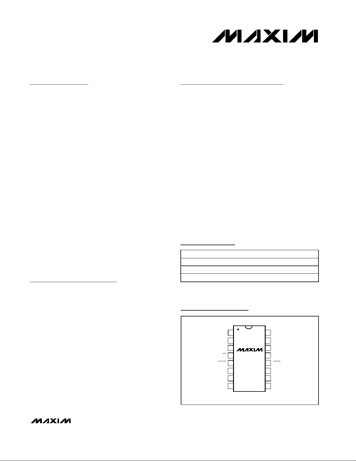
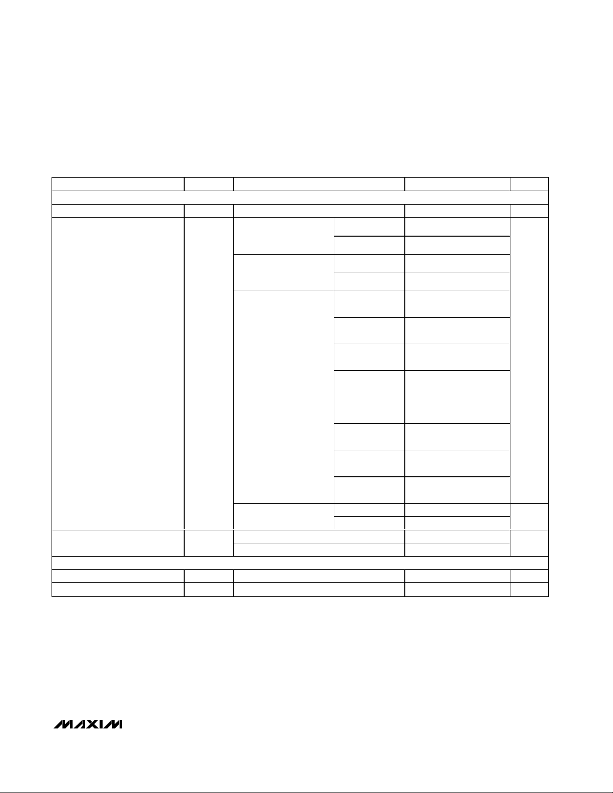
Pin Configuration
Ordering Information
19-3051; Rev 0; 10/03
For pricing, delivery, and ordering information, please contact Maxim/Dallas Direct! at
1-888-629-4642, or visit Maxim’s website at www.maxim-ic.com.
SPI/QSPI are trademarks of Motorola, Inc.
MICROWIRE is a trademark of National Semiconductor Corp.
*Future product—contact factory for availability.
PART TEMP RANGE PIN-PACKAGE
MX7705EPE* -40°C to +85°C 16 PDIP
MX7705EWE* -40°C to +85°C 16 WIDE SO
MX7705EUE -40°C to +85°C 16 TSSOP
TOP VIEW
SCLK
CLKIN
CLKOUT
RESET
AIN2+
AIN1+
AIN1-
1
2
3
MX7705
4
CS
5
6
7
8
16
GND
15
V
DD
DIN
14
DOUT
13
DRDY
12
AIN2-
11
REF-
10
REF+
9
PDIP/SO/TSSOP
Page 2
MX7705
16-Bit, Low-Power, 2-Channel,
Sigma-Delta ADC
2 _______________________________________________________________________________________
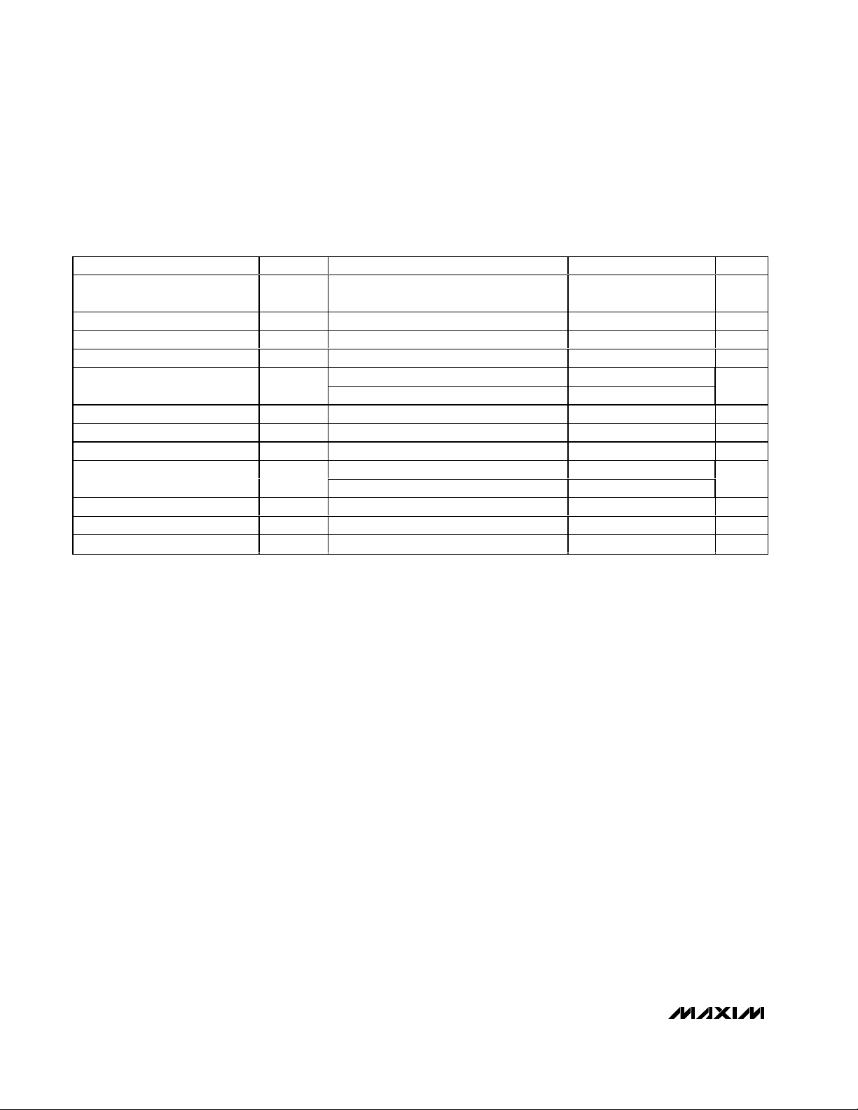
ABSOLUTE MAXIMUM RATINGS
ELECTRICAL CHARACTERISTICS
(VDD= 3V or 5V, GND = 0, V
REF+
= 1.225V for VDD= 3V and V
REF+
= 2.5V for VDD= 5V, V
REF-
= GND, external f
CLKIN
=
2.4576MHz, CLKDIV bit = 0, C
REF+
to GND = 0.1µF, C
REF
- to GND = 0.1µF, TA= T
MIN
to T
MAX
, unless otherwise noted.)
Stresses beyond those listed under “Absolute Maximum Ratings” may cause permanent damage to the device. These are stress ratings only, and functional
operation of the device at these or any other conditions beyond those indicated in the operational sections of the specifications is not implied. Exposure to
absolute maximum rating conditions for extended periods may affect device reliability.
VDDto GND..............................................................-0.3V to +6V
All Other Pins to GND.................................-0.3V to (V
DD
+ 0.3V)
Maximum Current Input into Any Pin ..................................50mA
Continuous Power Dissipation (T
A
= +70°C)
PDIP (derate 10.5mW/°C above +70°C)......................842mW
TSSOP (derate 9.4mW/°C above +70°C) ....................755mW
Wide SO (derate 9.5mW/°C above +70°C)..................762mW
Operating Temperature Range ..........................-40°C to +85°C
Storage Temperature Range .............................-60°C to +150°C
Junction Temperature......................................................+150°C
Lead Temperature (soldering, 10s) .................................+300°C
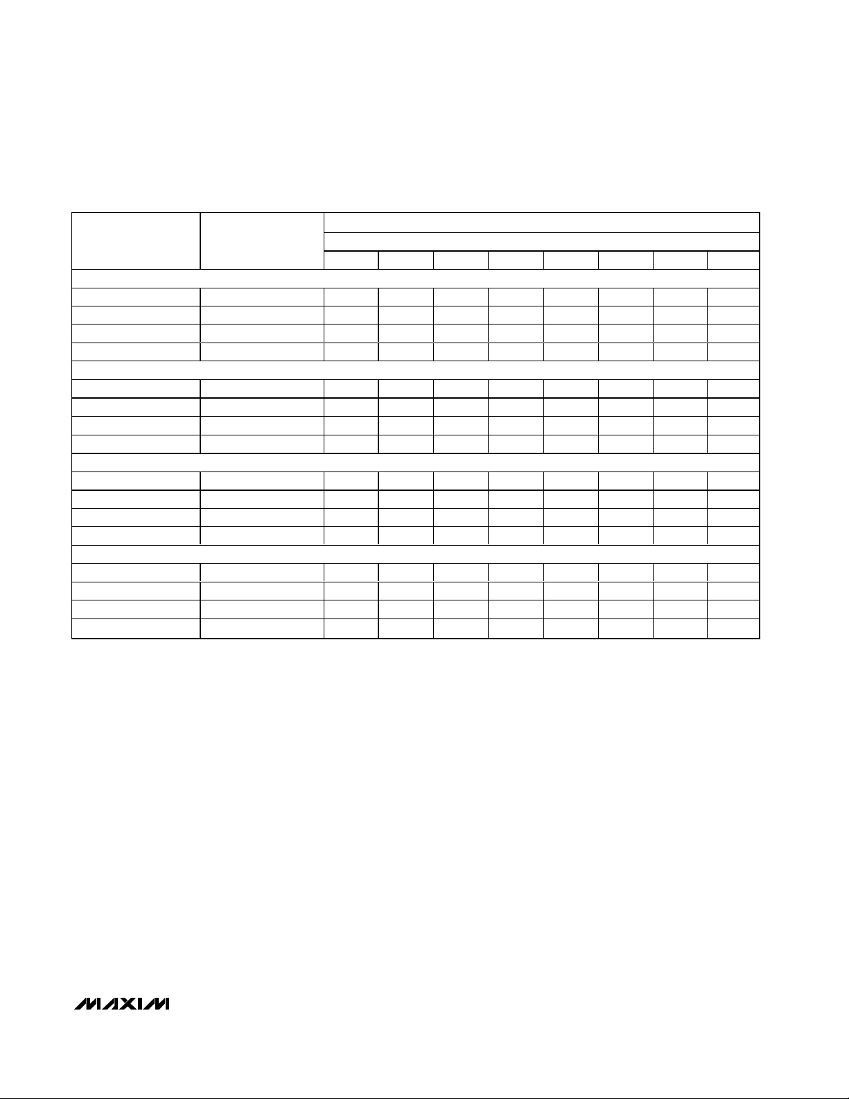
PARAMETER SYMBOL CONDITIONS MIN TYP MAX UNITS
DC ACCURACY
Resolution (No Missing Codes) 16 Bits
Output Noise Tables 1, 3 µV
Integral Nonlinearity INL Gain = 1, unbuffered ±0.003 %FSR
Unipolar Offset Error After calibration (Note 1) µV
Unipolar Offset Drift (Note 2) 0.5 µV/°C
Bipolar Zero Error After calibration (Note 1) µV
Bipolar Zero Drift (Note 2)
Positive Full-Scale Error After calibration (Notes 1, 3) µV
Full-Scale Drift (Notes 2, 4) 0.5 µV/°C
Gain Error After calibration (Notes 1, 5) µV
Gain Drift (Notes 2, 6) 0.5
Bipolar Negative Full-Scale Error After calibration ±0.003 %FSR
Bipolar Negative Full-Scale Drift
(Note 2)
ANALOG INPUTS (AIN1+, AIN1-, AIN2+, AIN2-)
AIN Differential Input Voltage
Range (Note 7)
AIN Absolute Input Voltage
Range (Note 8)
AIN DC Leakage Current Unselected input channel 1 nA
Gain = 1 to 4 0.5
Gain = 8 to 128 0.1
Gain = 1 to 4 1
Gain = 8 to 128 0.6
Unipolar input range 0
Bipolar input range
Unbuffered
Buffered
-V
GAIN
GND -
30mV
GND +
50mV
/
REF
V
REF
GAIN
V
REF
GAIN
V
DD
30mV
V
DD
1.5V
/
/
+
-
µV/°C
ppm of
FSR/°C
µV/°C
V
V
Page 3
MX7705
16-Bit, Low-Power, 2-Channel,
Sigma-Delta ADC
_______________________________________________________________________________________ 3
ELECTRICAL CHARACTERISTICS (continued)
(VDD= 3V or 5V, GND = 0, V
REF+
= 1.225V for VDD= 3V and V
REF+
= 2.5V for VDD= 5V, V
REF-
= GND, external f
CLKIN
=
2.4576MHz, CLKDIV bit = 0, C
REF+
to GND = 0.1µF, C
REF
- to GND = 0.1µF, TA= T
MIN
to T
MAX
, unless otherwise noted.)
PARAMETER SYMBOL CONDITIONS MIN TYP MAX UNITS
AIN Input Capacitance
AIN Input Sampling Rate f
Input Common-Mode Rejection CMR
Normal-Mode 50Hz Rejection
Normal-Mode 60Hz Rejection
Common-Mode 50Hz Rejection
Common-Mode 60Hz Rejection
EXTERNAL REFERENCE (REF+, REF-)
REF Differential Input Voltage
Range (Note 9)
RE F Ab sol ute Inp ut V ol tag e Rang e GND V
REF Input Capacitance Gain = 1 to 128 10 pF
REF Input Sampling Rate f
DIGITAL INPUTS (DIN, SCLK, CS, RESET)
Input High Voltage V
Input Low Voltage V
Input Hysteresis V
Input Current I
Input Capacitance 5pF
Gain = 1 34
Gain = 2 38
Gain = 4 45
Gain = 8 to 128 60
Gain = 1 to 128
s
VDD = 5V
V
DD
For filter notches of 25Hz, 50Hz,
±0.02 × f
For filter notches of 20Hz, 60Hz,
±0.02 × f
For filter notches of 25Hz, 50Hz,
±0.02 × f
For filter notches of 20Hz, 60Hz,
±0.02 × f
V
REF
HYST
IN
VDD = 4.75V to 5.25V 1.0 3.5
VDD = 2.7V to 3.6V 1.00 1.75
s
IH
VDD = 4.75V to 5.25V 0.8
IL
VDD = 2.7V to 3.6V 0.4
DIN, CS, RESET 250
SCLK 500
= 3V
NOTCH
NOTCH
NOTCH
NOTCH
Gain = 1 96
Gain = 2 105
Gain = 4 110
Gain = 8 to 128 130
Gain = 1 105
Gain = 2 110
Gain = 4 120
Gain = 8 to 128 130
f
CLKIN
64
98 dB
98 dB
150 dB
150 dB
f
CLKIN
64
2V
±1 µA
DD
pF
/
MHz
dB
V
V
/
MHz
V
mV
Page 4
MX7705
16-Bit, Low-Power, 2-Channel,
Sigma-Delta ADC
4 _______________________________________________________________________________________
ELECTRICAL CHARACTERISTICS (continued)
(VDD= 3V or 5V, GND = 0, V
REF+
= 1.225V for VDD= 3V and V
REF+
= 2.5V for VDD= 5V, V
REF-
= GND, external f
CLKIN
=
2.4576MHz, CLKDIV bit = 0, C
REF+
to GND = 0.1µF, C
REF
- to GND = 0.1µF, TA= T
MIN
to T
MAX
, unless otherwise noted.)
CLKIN INPUT
CLKIN Input High Voltage V
PARAMETER SYMBOL CONDITIONS MIN TYP MAX UNITS
CLKIN Input Low Voltage V
CLKIN Input Current I
DIGITAL OUTPUTS (DOUT, DRDY, CLKOUT)
Output Voltage Low V
Output Voltage High V
Tri-State Leakage Current I
Tri-State Output Capacitance C
SYSTEM CALIBRATION
Full-Scale Calibration Range
CLKINH
CLKINL
CLKIN
OH
OUT
VDD = 4.75V to 5.25V 3.5
VDD = 2.7V to 3.6V 2.5
VDD = 4.75V to 5.25V 0.8
VDD = 2.7V to 3.6V 0.4
VDD = 5V
OL
VDD = 3V
VDD = 5V
VDD = 3V
DOUT only ±10 µA
L
DOUT only 9 pF
GAIN = selected PGA gain (1 to 128)
(Note 10)
DOUT and DRDY,
I
= 800µA
SINK
CLKOUT,
I
= 10µA
SINK
DOUT and DRDY,
I
= 100µA
SINK
CLKOUT,
I
= 10µA
SINK
DOUT and DRDY,
I
CLKOUT,
I
DOUT and DRDY,
I
CLKOUT,
I
SOURCE
SOURCE
SOURCE
SOURCE
= 200µA
= 10µA
= 100µA
= 10µA
4.0
4.0
V
DD
0.6V
V
DD
0.6V
-1.05 ×
V
REF
GAIN
-
-
/
±10 µA
0.4
0.4
0.4
0.4
1.05 ×
V
/
REF
GAIN
V
V
V
V
V
-1.05 ×
V
REF
GAIN
0.8 ×
V
REF
GAIN
/
/
Offset Calibration Range
Input Span
GAIN = selected PGA gain (1 to 128)
(Note 10)
GAIN = selected PGA gain (1 to 128)
(Notes 10, 11)
1.05 ×
V
REF
GAIN
2.1 ×
V
REF
GAIN
/
V
/
V
Page 5
MX7705
16-Bit, Low-Power, 2-Channel,
Sigma-Delta ADC
_______________________________________________________________________________________ 5
ELECTRICAL CHARACTERISTICS (continued)
(VDD= 3V or 5V, GND = 0, V
REF+
= 1.225V for VDD= 3V and V
REF+
= 2.5V for VDD= 5V, V
REF-
= GND, external f
CLKIN
=
2.4576MHz, CLKDIV bit = 0, C
REF+
to GND = 0.1µF, C
REF
- to GND = 0.1µF, TA= T
MIN
to T
MAX
, unless otherwise noted.)
POWER REQUIREMENTS
Power-Supply Voltage V
Power-Supply Current (Note 12) I
Power-Supply Rejection Ratio PSRR
EXTERNAL CLOCK TIMING SPECIFICATIONS
CLKIN Frequency f
Duty Cycle 40 60 %
PARAMETER SYMBOL CONDITIONS MIN TYP MAX UNITS
DD
Unbuffered
f
CLKIN
gain =1 to 128
Buffered,
f
CLKIN
gain =1 to 128
Unbuffered,
f
CLKIN
DD
Buffered,
f
CLKIN
Power-down mode
(Note 13)
VDD = 4.75V to 5.25V (Note 14)
V
DD
CLKIN
(Note 15) 400 2500 kHz
=1MHz,
=1MHz,
= 2.4576MHz
= 2.4576MHz
= 2.7V to 3.6V (Note 14)
VDD = 5V 0.45
V
DD
VDD = 5V 0.7
V
DD
VDD = 5V,
gain = 1 to 4
VDD = 5V,
gain = 8 to 128
VDD = 3V,
gain = 1 to 4
V
DD
gain = 8 to 128
VDD = 5V,
gain = 1 to 4
VDD = 5V,
gain = 8 to 128
VDD = 3V,
gain = 1 to 4
V
DD
gain = 8 to 128
VDD = 5V 16
V
DD
= 3V 0.32
= 3V 0.6
= 3V,
= 3V,
= 3V 8
2.70 5.25 V
0.6
0.85
0.4
0.6
0.9
1.3
0.7
1.1
mA
µA
dB
Page 6
MX7705
16-Bit, Low-Power, 2-Channel,
Sigma-Delta ADC
6 _______________________________________________________________________________________
TIMING CHARACTERISTICS
(VDD= 3V or 5V, GND = 0, V
REF+
= 1.225V for VDD= 3V and V
REF+
= 2.5V for VDD= 5V, V
REF-
= GND, external f
CLKIN
=
2.4576MHz, CLKDIV bit = 0, C
REF+
to GND = 0.1µF, C
REF
- to GND = 0.1µF, TA= T
MIN
to T
MAX
, unless otherwise noted.) (Note 16)
(Figures 8, 9)
DRDY High Time
Reset Pulse-Width Low 100 ns
DRDY Fall to CS Fall Setup Time t
CS Fall to SCLK Rise Setup Time t
SCLK Fall to DOUT Valid Delay t
SCLK Pulse-Width High t
SCLK Pulse-Width Low t
CS Rise to SCLK Rise Hold Time t
Bus Relinquish Time After SCLK
Rising Edge
SCLK Fall to DRDY Rise Delay t
DIN to SCLK Setup Time t
DIN to SCLK Hold Time t
PARAMETER SYMBOL CONDITIONS MIN TYP MAX UNITS
1
2
VDD = 4.75V to 5.25V 0 80
3
VDD = 2.7V to 3.6V 0 100
4
5
6
t
10
VDD = 4.75V to 5.25V 60
7
VDD = 2.7V to 3.6V 100
8
9
500 /
f
CLKIN
120 ns
100 ns
100 ns
30 ns
20 ns
0ns
0ns
100 ns
s
ns
ns
Page 7
MX7705
16-Bit, Low-Power, 2-Channel,
Sigma-Delta ADC
_______________________________________________________________________________________ 7
Note 1: These errors are in the order of the conversion noise shown in Tables 1 and 3. This applies after calibration at the given
temperature.
Note 2: Recalibration at any temperature removes these drift errors.
Note 3: Positive full-scale error includes zero-scale errors (unipolar offset error or bipolar zero error) and applies to both unipolar
and bipolar input ranges.
Note 4: Full-scale drift includes zero-scale drift (unipolar offset drift or bipolar zero drift) and applies to both unipolar and bipolar
input ranges.
Note 5: Gain error does not include zero-scale errors. It is calculated as (full-scale error - unipolar offset error) for unipolar ranges,
and (full-scale error - bipolar zero error) for bipolar ranges.
Note 6: Gain-error drift does not include unipolar offset drift or bipolar zero drift. Effectively, it is the drift of the part if only zero-
scale calibrations are performed.
Note 7: The analog input voltage range on AIN+ is given with respect to the voltage on AIN- on the MX7705.
Note 8: This common-mode voltage range is allowed, provided that the input voltage on analog inputs does not go more positive
than (V
DD
+ 30mV) or more negative than (GND - 30mV). Parts are functional with voltages down to (GND - 200mV), but
with increased leakage at high temperature.
Note 9: The REF differential voltage, V
REF
, is the voltage on REF+ referenced to REF- (V
REF
= V
REF+
- V
REF-)
.
Note 10: Guaranteed by design.
Note 11: These calibration and span limits apply, provided that the absolute voltage on the analog inputs does not exceed (V
DD
+
30mV) or go more negative than (GND - 30mV). The offset calibration limit applies to both the unipolar zero point and the
bipolar zero point.
Note 12: When using a crystal or ceramic resonator across the CLKIN and CLKOUT as the clock source for the device, the supply
current and power dissipation varies depending on the crystal or resonator type. Supply current is measured with the digital inputs connected to 0 or V
DD
, CLKIN connected to an external clock source, and CLKDIS = 1.
Note 13: If the external master clock continues to run in power-down mode, the power-down current typically increases to 67µA at
3V. When using a crystal or ceramic resonator across the CLKIN and CLKOUT as the clock source for the device, the
clock generator continues to run in power-down mode and the power dissipation depends on the crystal or resonator type
(see the Power-Down Modes section).
Note 14: Measured at DC and applied in the selected passband. PSRR at 50Hz exceeds 120dB with filter notches of 25Hz or 50Hz.
PSRR at 60Hz exceeds 120dB with filter notches of 20Hz or 60Hz. PSRR depends on both gain and V
DD
.
Note 15: Provide f
CLKIN
whenever the MX7705 is not in power-down mode. If no clock is present, the device can draw higher than
specified current and can possibly become uncalibrated.
Note 16: All input signals are specified with t
r
= tf= 5ns (10% to 90% of VDD) and timed from a voltage level of 1.6V.
TIMING CHARACTERISTICS (continued)
(VDD= 3V or 5V, GND = 0, V
REF+
= 1.225V for VDD= 3V and V
REF+
= 2.5V for VDD= 5V, V
REF-
= GND, external f
CLKIN
=
2.4576MHz, CLKDIV bit = 0, C
REF+
to GND = 0.1µF, C
REF
- to GND = 0.1µF, TA= T
MIN
to T
MAX
, unless otherwise noted.) (Note 16)
(Figures 8, 9)
GAIN
19086
27878
48485
8 to 128 91 93
PSRR (dB)
(V
= 5V)
DD
PSRR (dB)
(VDD = 3V)
Page 8
MX7705
16-Bit, Low-Power, 2-Channel,
Sigma-Delta ADC
8 _______________________________________________________________________________________
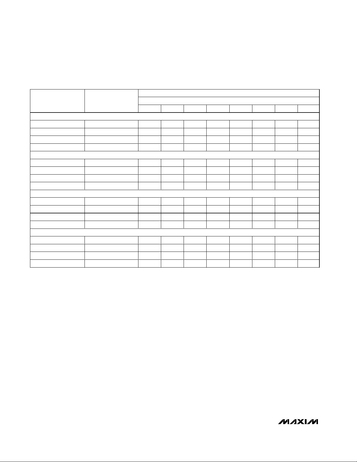
Table 1. Output RMS Noise vs. Gain and Output Data Rate (VDD= 5V)
FILTER FIRST
NOTCH AND
OUTPUT DATA RATE
BUFFERED (f
UNBUFFERED (f
BUFFERED (f
UNBUFFERED (f
CLKIN
20Hz 5.24Hz 4.44 2.28 1.29 0.79 0.70 0.70 0.64 0.63
25Hz 6.55Hz 5.11 2.79 1.55 0.92 0.81 0.80 0.73 0.74
100Hz 26.2Hz 102.35 49.59 23.04 11.78 6.32 3.63 2.25 2.24
200Hz 52.4Hz 586.93 272.83 224.79 70.78 33.94 17.57 9.14 9.22
20Hz 5.24Hz 4.32 2.50 1.35 0.81 0.73 0.70 0.64 0.64
25Hz 6.55Hz 5.16 2.85 1.63 0.96 0.83 0.81 0.74 0.74
100Hz 26.2Hz 105.78 49.86 24.67 12.16 6.42 3.80 2.22 2.23
200Hz 52.4Hz 526.60 260.51
CLKIN
50Hz 13.1Hz 3.53 1.86 1.09 0.73 0.72 0.71 0.67 0.66
60Hz 15.72Hz 4.41 2.23 1.29 0.83 0.79 0.77 0.72 0.73
250Hz 65.5Hz 99.66 46.85 16.98 12.48 6.38 3.78 2.32 2.35
500Hz 131Hz 608.86 288.39 110.80 67.51 36.75 17.98 9.43 9.40
50Hz 13.1Hz 3.65 1.94 1.17 0.79 0.70 0.69 0.66 0.65
60Hz 15.72Hz 4.56 2.41 1.32 0.87 0.80 0.79 0.71 0.74
250Hz 65.5Hz 101.56 49.64 25.39 12.92 6.65 3.69 2.36 2.36
500Hz 131Hz 556.06 278.91 142.88 74.78 35.41 18.99 9.80 9.44
CLKIN
CLKIN
-3dB FREQUENCY
1 2 4 8 16 32 64 128
= 1MHz)
= 1MHz)
= 2.4576MHz)
= 2.4576MHz)
TYPICAL OUTPUT RMS NOISE (µV)
GAIN
132.16
67.25 34.09 18.20 8.95 9.08
Page 9
MX7705
16-Bit, Low-Power, 2-Channel,
Sigma-Delta ADC
_______________________________________________________________________________________ 9
Table 2. Peak-to-Peak Resolution vs. Gain and Output Data Rate (VDD= 5V)
FILTER FIRST
NOTCH AND
OUTPUT DATA RATE
BUFFERED (f
UNBUFFERED (f
BUFFERED (f
UNBUFFERED (f
CLKIN
20Hz 5.24Hz 16 16 16 16 16 15 14 13
25Hz 6.55Hz 16 16 16 16 16 15 14 13
100Hz 26.2Hz 12 12 12 12 12 12 12 11
200Hz 52.4Hz 10 10 10 10 10 10 10 9
CLKIN
20Hz 5.24Hz 16 16 16 16 16 15 14 13
25Hz 6.55Hz 16 16 16 16 16 15 14 13
100Hz 26.2Hz 12 12 12 12 12 12 12 11
200Hz 52.4Hz 10 10 10 10 10 10 10 9
CLKIN
50Hz 13.1Hz 16 16 16 16 16 15 14 13
60Hz 15.72Hz 16 16 16 16 16 15 14 13
250Hz 65.5Hz 12 12 13 12 12 12 12 11
500Hz 131Hz 10 10 11 10 10 10 10 9
CLKIN
50Hz 13.1Hz 16 16 16 16 16 15 14 13
60Hz 15.72Hz 16 16 16 16 16 15 14 13
250Hz 65.5Hz 12 12 12 12 12 12 12 11
500Hz 131Hz 10 10 10 10 10 10 10 9
-3dB FREQUENCY
1 2 4 8 16 32 64 128
= 1MHz)
= 1MHz)
= 2.4576MHz)
= 2.4576MHz)
TYPICAL PEAK-TO-PEAK RESOLUTION (BITS)
GAIN
Page 10
MX7705
16-Bit, Low-Power, 2-Channel,
Sigma-Delta ADC
10 ______________________________________________________________________________________
Table 3. Output RMS Noise vs. Gain and Output Data Rate (VDD= 3V)
FILTER FIRST
NOTCH AND
OUTPUT DATA RATE
BUFFERED (f
UNBUFFERED (f
BUFFERED (f
UNBUFFERED (f
CLKIN
20Hz 5.24Hz 3.52 1.84 2.19 0.73 0.66 0.62 0.62 0.62
25Hz 6.55Hz 4.24 2.23 1.19 0.84 0.74 0.69 0.69 0.69
100Hz 26.2Hz 50.36 25.12 12.06 6.04 3.38 2.23 1.70 1.69
200Hz 52.4Hz 268.02 175.98 65.77 34.89 16.73 8.76 4.70 4.70
20Hz 5.24Hz 3.58 1.92 1.13 0.72 0.66 0.64 0.61 0.62
25Hz 6.55Hz 4.16 2.27 1.27 0.83 0.74 0.70 0.69 0.67
100Hz 26.2Hz 50.48 23.89 12.10 5.90 3.26 0.70 1.66 1.63
200Hz 52.4Hz 256.43 135.78 65.62 33.18 16.65 8.47 4.66 4.68
CLKIN
50Hz 13.1Hz 2.84 1.68 2.00 0.71 0.67 0.65 0.63 0.61
60Hz 15.72Hz 3.27 1.84 1.12 0.78 0.75 0.70 0.68 0.67
250Hz 65.5Hz 47.90 24.43 12.56 6.48 3.45 2.32 1.64 1.66
500Hz 131Hz 281.03 104.19 69.58 34.59 17.44 9.20 5.16 4.92
50Hz 13.1Hz 3.04 1.74 1.03 0.72 0.64 0.64 0.62 0.63
60Hz 15.72Hz 3.35 1.80 1.13 0.81 0.73 0.69 0.67 0.68
250Hz 65.5Hz 49.63 23.82 13.03 6.23 3.42 2.22 1.68 1.65
500Hz 131Hz 279.13 134.82 69.47 35.42 17.47 9.55 4.90 5.18
CLKIN
CLKIN
-3dB FREQUENCY
1248163264128
= 1MHz)
= 1MHz)
= 2.4576MHz)
= 2.4576MHz)
TYPICAL OUTPUT RMS NOISE (µV)
GAIN
Page 11
MX7705
16-Bit, Low-Power, 2-Channel,
Sigma-Delta ADC
______________________________________________________________________________________ 11
Table 4. Peak-to-Peak Resolution vs. Gain and Output Data Rate (VDD= 3V)
Typical Operating Characteristics
(VDD= 3V or 5V, V
REF+
= 1.225V for VDD= 3V, V
REF+
= 2.5V for VDD= 5V, V
REF
- = GND, TA= +25°C, unless otherwise noted.)
FILTER FIRST
NOTCH AND
OUTPUT DATA RATE
BUFFERED (f
CLKIN
-3dB FREQUENCY
1 2 4 8 16 32 64 128
= 1MHz)
TYPICAL PEAK-TO-PEAK RESOLUTION (BITS)
GAIN
20Hz 5.24Hz 16 16 16 16 15 14 13 12
25Hz 6.55Hz 16 16 16 16 15 14 13 12
100Hz 26.2Hz 12 12 12 12 12 12 12 11
200Hz 52.4Hz 10 10 10 10 10 10 10 9
UNBUFFERED (f
CLKIN
= 1MHz)
20Hz 5.24Hz 16 16 16 16 15 14 13 12
25Hz 6.55Hz 16 16 16 16 15 14 13 12
100Hz 26.2Hz 12 12 12 12 12 14 12 11
200Hz 52.4Hz 10 10 10 10 10 10 10 9
BUFFERED (f
= 2.4576MHz)
CLKIN
50Hz 13.1Hz 16 16 16 16 15 14 13 12
60Hz 15.72Hz 16 16 16 16 15 14 13 12
250Hz 65.5Hz 12 12 12 12 12 12 11 11
500Hz 131Hz 10 11 10 10 10 10 10 9
UNBUFFERED (f
= 2.4576MHz)
CLKIN
50Hz 13.1Hz 16 16 16 16 15 14 13 12
60Hz 15.72Hz 16 16 16 16 15 14 13 12
250Hz 65.5Hz 12 12 12 12 12 12 11 11
500Hz 131Hz 10 10 10 10 10 10 10 9
32776
32774
32772
32770
32768
32766
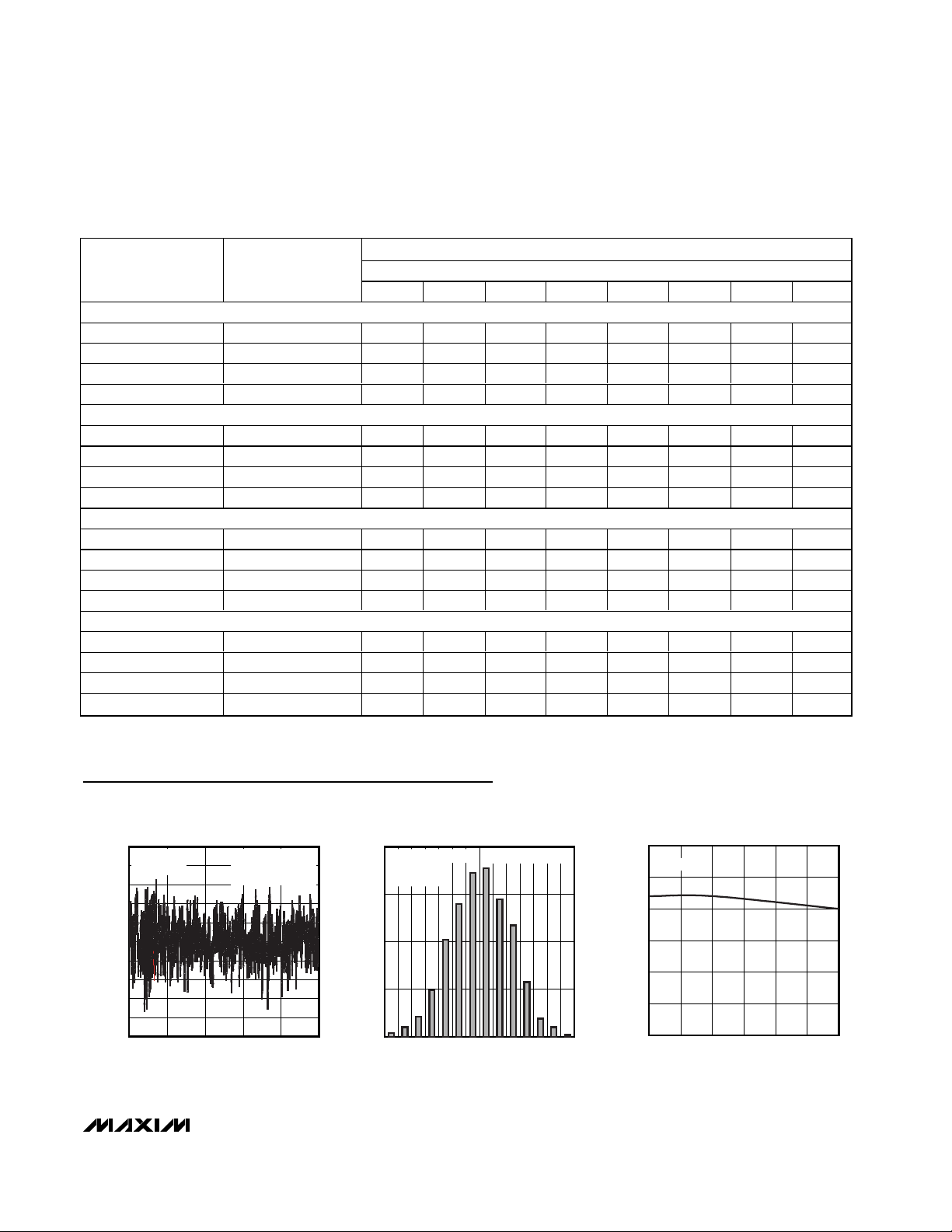
CODE READ
32764
32762
32760
32758
32756
TYPICAL OUTPUT NOISE
VDD = 5V,
= 2.5V
V
REF
0 2000
READING NUMBER
GAIN = 128
ODR = 60Hz
RMS NOISE = 1.3µV
16001200800400
MX7705 toc01
HISTOGRAM OF TYPICAL OUTPUT NOISE
400
VDD = 5V, V
GAIN = 128
ODR = 60Hz
300
200
OCCURENCE
100
0
32760
32761
REF
32762
= 2.5V
32763
32764
32765
CODE
RMS NOISE = 1.3µV
32768
32767
32766
32769
32770
32771
32772
MX7705 toc02
32773
OFFSET ERROR vs. SUPPLY VOLTAGE (3V)
0.0015
0.0010
0.0005
-0.0005
OFFSET ERROR (%FSR)
-0.0010
-0.0015
VDD = 3V
0
2.70 3.60
SUPPLY VOLTAGE (V)
MX7705 toc03
3.453.303.153.002.85
Page 12

MX7705
16-Bit, Low-Power, 2-Channel,
Sigma-Delta ADC
12 ______________________________________________________________________________________
Typical Operating Characteristics (continued)
(VDD= 3V or 5V, V
REF+
= 1.225V for VDD= 3V, V
REF+
= 2.5V for VDD= 5V, V
REF
- = GND, TA= +25°C, unless otherwise noted.)
OFFSET ERROR vs. SUPPLY VOLTAGE (5V)
0.003
VDD = 5V
0.002
0.001
MX7705 toc04
OFFSET ERROR vs. TEMPERATURE
0.003
0.002
0.001
VDD = 5V
GAIN ERROR vs. SUPPLY VOLTAGE (3V)
0.0015
VDD = 3V
MX7705 toc05
0.0010
0.0005
MX7705 toc06
0
-0.001
OFFSET ERROR (%FSR)
-0.002
-0.003
4.75 5.25
SUPPLY VOLTAGE (V)
GAIN ERROR vs. SUPPLY VOLTAGE (5V)
0.003
VDD = 5V
0.002
0.001
0
-0.001
GAIN ERROR (%FSR)
-0.002
-0.003
4.75 5.25
5.155.054.954.85
SUPPLY VOLTAGE (V)
0
-0.001
OFFSET ERROR (%FSR)
-0.002
-0.003
VDD = 3V
-40 85
TEMPERATURE (°C)
MX7705 toc07
-0.001
GAIN ERROR (%FSR)
-0.002
-0.003
-0.004
5.155.054.954.85
-0.005
0
-0.0005
GAIN ERROR (%FSR)
-0.0010
603510-15
-0.0015
2.70 3.60
GAIN ERROR vs. TEMPERATURE
0.005
0.004
0.003
0.002
0.001
VDD = 3V
0
VDD = 5V
-40 85
TEMPERATURE (°C)
3.453.303.153.002.85
SUPPLY VOLTAGE (V)
MX7705 toc08
603510-15
Page 13

MX7705
16-Bit, Low-Power, 2-Channel,
Sigma-Delta ADC
______________________________________________________________________________________ 13
Typical Operating Characteristics (continued)
(VDD= 3V or 5V, V
REF+
= 1.225V for VDD= 3V, V
REF+
= 2.5V for VDD= 5V, V
REF
- = GND, TA= +25°C, unless otherwise noted.)
A: BUFFERED MODE
f
CLKIN
GAIN = 8 TO 128
D: UNBUFFERED MODE
f
CLKIN
GAIN = 1 TO 128
SUPPLY CURRENT vs. SUPPLY VOLTAGE (3V)
0.6
A
0.5
B
0.4
C
SUPPLY CURRENT (mA)
D
0.3
E
0.2
2.70 3.60
SUPPLY VOLTAGE (V)
= 2.4576MHz,
= 2.4576MHz,
B: BUFFERED MODE
= 2.4576MHz,
f
CLKIN
GAIN = 1 TO 4
E: UNBUFFERED MODE
= 1MHz,
f
CLKIN
GAIN = 1 TO 128
VDD = 3V
3.453.303.153.002.85
C: BUFFERED MODE
f
CLKIN
GAIN = 1 TO 128
MX7705 toc09
= 1MHz,
SUPPLY CURRENT vs. SUPPLY VOLTAGE (5V)
0.65
A
0.55
0.45
C
SUPPLY CURRENT (mA)
0.35
E
0.25
4.75 5.25
A: BUFFERED MODE
f
= 2.4576MHz,
CLKIN
GAIN = 8 TO 128
D: UNBUFFERED MODE
= 2.4576MHz,
f
CLKIN
GAIN = 1 TO 128
VDD = 5V
D
SUPPLY VOLTAGE (V)
B: BUFFERED MODE
= 2.4576MHz,
f
CLKIN
GAIN = 1 TO 4
E: UNBUFFERED MODE
= 1MHz,
f
CLKIN
GAIN = 1 TO 128
B
5.155.054.954.85
C: BUFFERED MODE
= 1MHz,
f
CLKIN
GAIN = 1 TO 128
MX7705 toc10
SUPPLY CURRENT vs. TEMPERATURE (3V)
0.6
A
0.5
C
0.4
SUPPLY CURRENT (mA)
0.3
0.2
-40 85
A: BUFFERED MODE
= 2.4576MHz,
f
CLKIN
GAIN = 8 TO 128
D: UNBUFFERED MODE
= 2.4576MHz,
f
CLKIN
GAIN = 1 TO 128
D
E
TEMPERATURE (°C)
B: BUFFERED MODE
f
CLKIN
GAIN = 1 TO 4
E: UNBUFFERED MODE
f
CLKIN
GAIN = 1 TO 128
= 2.4576MHz,
= 1MHz,
VDD = 3V
B
603510-15
C: BUFFERED MODE
= 1MHz,
f
CLKIN
GAIN = 1 TO 128
MX7705 toc11
SUPPLY CURRENT vs. TEMPERATURE (5V)
0.65
A
0.55
C
0.45
SUPPLY CURRENT (mA)
0.35
E
0.25
-40 85
A: BUFFERED MODE
= 2.4576MHz,
f
CLKIN
GAIN = 8 TO 128
D: UNBUFFERED MODE
= 2.4576MHz,
f
CLKIN
GAIN = 1 TO 128
VDD = 5V
D
TEMPERATURE (°C)
B: BUFFERED MODE
= 2.4576MHz,
f
CLKIN
GAIN = 1 TO 4
E: UNBUFFERED MODE
= 1MHz,
f
CLKIN
GAIN = 1 TO 128
B
603510-15
C: BUFFERED MODE
= 1MHz,
f
CLKIN
GAIN = 1 TO 128
MX7705 toc12
Page 14

MX7705
16-Bit, Low-Power, 2-Channel,
Sigma-Delta ADC
14 ______________________________________________________________________________________
Typical Operating Characteristics (continued)
(VDD= 3V or 5V, V
REF+
= 1.225V for VDD= 3V, V
REF+
= 2.5V for VDD= 5V, V
REF
- = GND, TA= +25°C, unless otherwise noted.)
SUPPLY CURRENT vs. f
0.6
VDD = 3V
A
0.5
0.4
C
SUPPLY CURRENT (mA)
0.3
E
0.2
A: BUFFERED MODE
CLK = 1,
GAIN = 128
D: UNBUFFERED MODE
CLK = 1,
GAIN = 1, 128
SUPPLY CURRENT vs. GAIN (3V)
0.6
VDD = 3V
0.5
D
f
(MHz)
CLKIN
B: BUFFERED MODE
CLK = 1,
GAIN = 1
E: UNBUFFERED MODE
CLK = 0,
GAIN = 1, 128
A
(3V)
CLKIN
B
2.22.01.81.61.41.21.00.80.60.4 2.6
2.4
C: BUFFERED MODE
CLK = 0,
GAIN = 1, 128
B
MX7705 toc13
MX7705 toc15
SUPPLY CURRENT vs. f
0.65
VDD = 5V
0.55
0.45
SUPPLY CURRENT (mA)
0.35
0.25
A: BUFFERED MODE
CLK = 1,
GAIN = 128
D: UNBUFFERED MODE
CLK = 1,
GAIN = 1, 128
A
C
SUPPLY CURRENT vs. GAIN (5V)
0.65
VDD = 5V
0.55
D
E
f
(MHz)
CLKIN
B: BUFFERED MODE
CLK = 1,
GAIN = 1
E: UNBUFFERED MODE
CLK = 0,
GAIN = 1, 128
A
B
(5V)
CLKIN
B
2.22.01.81.61.41.21.00.80.60.4 2.6
2.4
C: BUFFERED MODE
CLK = 0,
GAIN = 1, 128
MX7705 toc14
MX7705 toc16
0.4
SUPPLY CURRENT (mA)
0.3
0.2
A: BUFFERED MODE
CLK = 1, CLKDIV = 1,
= 2.4576MHz
f
CLKIN
D: UNBUFFERED MODE
CLK = 1, CLKDIV = 1,
= 2.4576MHz
f
CLKIN
C
D
F
GAIN
B: BUFFERED MODE
CLK = 1, CLKDIV = 0,
= 2.4576MHz
f
CLKIN
E: UNBUFFERED MODE
CLK = 1, CLKDIV = 0,
= 2.4576MHz
f
CLKIN
E
32168421 128
C: BUFFERED MODE
CLK = 0, CLKDIV = 0,
f
F: UNBUFFERED MODE
CLK = 0, CLKDIV = 0,
f
64
CLKIN
CLKIN
= 1MHz
= 1MHz
0.45
SUPPLY CURRENT (mA)
0.35
0.25
A: BUFFERED MODE
CLK = 1, CLKDIV = 0,
= 2.4576MHz
f
CLKIN
D: UNBUFFERED MODE
CLK = 1, CLKDIV = 1,
= 2.4576MHz
f
CLKIN
C
D
E
F
GAIN
B: BUFFERED MODE
CLK = 1, CLKDIV = 1,
= 2.4576MHz
f
CLKIN
E: UNBUFFERED MODE
CLK = 1, CLKDIV = 0,
= 2.4576MHz
f
CLKIN
32168421 128
C: BUFFERED MODE
CLK = 0, CLKDIV = 0,
f
F: UNBUFFERED MODE
CLK = 0, CLKDIV = 0,
f
64
CLKIN
CLKIN
= 1MHz
= 1MHz
Page 15

MX7705
16-Bit, Low-Power, 2-Channel,
Sigma-Delta ADC
______________________________________________________________________________________ 15
Typical Operating Characteristics (continued)
(VDD= 3V or 5V, V
REF+
= 1.225V for VDD= 3V, V
REF+
= 2.5V for VDD= 5V, V
REF
- = GND, TA= +25°C, unless otherwise noted.)
POWER-DOWN SUPPLY CURRENT
vs. SUPPLY VOLTAGE (3V)
100
VDD = 3V
80
60
40
20
POWER-DOWN SUPPLY CURRENT (nA)
0
2.70 3.60
SUPPLY VOLTAGE (V)
POWER-DOWN SUPPLY CURRENT
vs. SUPPLY VOLTAGE (5V)
200
VDD = 5V
MX7705 toc17
180
160
140
120
POWER-DOWN SUPPLY CURRENT (nA)
3.453.303.153.002.85
100
4.75 5.25
SUPPLY VOLTAGE (V)
EXTERNAL OSCILLATOR STARTUP TIME
POWER-DOWN SUPPLY CURRENT
vs. TEMPERATURE
300
MX7705 toc18
5.155.054.954.85
MX7705 toc20
250
200
150
100
50
POWER-DOWN SUPPLY CURRENT (µA)
0
-40 85
VDD = 5V
VDD = 3V
TEMPERATURE (°C)
MX7705 toc19
603510-15
V
DD
5V/div
4.9152MHz CRYSTAL
2.4576MHz CRYSTAL
2ms/div
CLKOUT
5V/div
CLKOUT
5V/div
Page 16

MX7705
16-Bit, Low-Power, 2-Channel,
Sigma-Delta ADC
16 ______________________________________________________________________________________
Pin Description
PIN NAME FUNCTION
1 SCLK
2 CLKIN
3 CLKOUT
4 CS
5 RESET Active-Low Reset Input. Drive RESET low to reset the MX7705 to power-on reset status.
6 AIN2+ Channel 2 Positive Differential Analog Input
7 AIN1+ Channel 1 Positive Differential Analog Input
8 AIN1- Channel 1 Negative Differential Analog Input
9 REF+ Positive Differential Reference Input
10 REF- Negative Differential Reference Input
11 AIN2- Channel 2 Negative Differential Analog Input
12 DRDY
13 DOUT
14 DIN Serial Data Input. Data on DIN is clocked in on the rising edge of SCLK when CS is low.
15 V
16 GND Ground
DD
Serial Clock Input. Apply an external serial clock to transfer data to and from the device at data rates
of up to 5MHz.
Clock Input. Connect a crystal/resonator between CLKIN and CLKOUT, or drive CLKIN externally with
a CMOS-compatible clock source with CLKOUT left unconnected.
Clock Output. Connect a crystal/resonator between CLKIN and CLKOUT. When enabled, CLKOUT
provides a CMOS-compatible, inverted clock output. Set CLKDIS = 0 in the clock register to enable
CLKOUT. Set CLKDIS = 1 in the clock register to disable CLKOUT to conserve power.
Active-Low Chip-Select Input. CS selects the active device in systems with more than one device on
the serial bus. Drive CS low to clock data in on DIN and to clock data out on DOUT. When CS is high,
DOUT is high impedance. Connect CS to GND for 3-wire operation.
Active-Low Data-Ready Output. DRDY goes low when a new conversion result is available in the data
register. When a read-operation of a full output word completes, DRDY returns high.
Serial Data Output. DOUT outputs serial data from the data register. DOUT changes on the falling
edge of SCLK and is valid on the rising edge of SCLK. When CS is high, DOUT is high impedance.
Power Input
Page 17

Detailed Description
The MX7705 low-power, 2-channel, serial-output ADC
uses a sigma-delta modulator with a digital filter to
achieve 16-bit resolution with no missing codes. The
device includes a PGA, an on-chip input buffer, and a
bidirectional communications port. The MX7705 operates with a single 2.7V to 5.25V supply.
Fully differential inputs, an internal input buffer, and an
on-chip PGA (gain = 1 to 128) allow low-level signals to
be directly measured, minimizing the requirements for
external signal conditioning. Self-calibration corrects for
gain and offset errors. A programmable digital filter
allows for the selection of the output data rate and firstnotch frequency from 20Hz to 500Hz.
The bidirectional serial SPI-/QSPI-/MICROWIRE-compatible interface consists of four digital control lines (SCLK,
CS, DOUT, and DIN) and provides an easy interface to
microcontrollers (µCs). Connect CS to GND to configure
the MX7705 for 3-wire operation.
Analog Inputs
The MX7705 accepts four analog inputs (AIN1+, AIN1-,
AIN2+, and AIN2-) in buffered or unbuffered mode.
Use Table 8 to select the positive and negative input
pair for a fully differential channel. The input buffer isolates the inputs from the capacitive load presented by
the PGA/modulator, allowing for high source-impedance analog transducers. The value of the BUF bit in
the setup register (see the Setup Register section) determines whether the input buffer is enabled or disabled.
Internal protection diodes, which clamp the analog
input to VDDand/or GND, allow the input to swing from
(GND - 0.3V) to (VDD+ 0.3V), without damaging the
device. If the analog input exceeds 300mV beyond the
supplies, limit the input current to 10mA.
Input Buffers
When the analog input buffer is disabled, the analog
input drives a typical 7pF (gain = 1) capacitor, C
TOTAL
,
in series with the 7kΩ typical on-resistance of the track
and hold (T/H) switch (Figure 1). C
TOTAL
is comprised
of the sampling capacitor, C
SAMP
, and the stray capac-
itance, C
STRAY
. During the conversion, C
SAMP
charges
to (AIN+ - AIN-). The gain determines the value of
C
SAMP
(Table 5).
MX7705
16-Bit, Low-Power, 2-Channel,
Sigma-Delta ADC
______________________________________________________________________________________ 17
Functional Diagram
MX7705
BUFFER
AIN1+
AIN1-
AIN2+
AIN2-
REF+
REF-
SWITCHING
NETWORK
S1
S2
BUFFER
S1 AND S2 ARE OPEN IN
BUFFERED MODE AND CLOSED
IN UNBUFFERED MODE
PGA
DIVIDER
2ND-ORDER
SIGMA-DELTA
MODULATOR
SERIAL INTERFACE,
REGISTERS,
CLOCK
GENERATOR
DIGITAL
FILTER
AND
CONTROL
CLKIN
CLKOUT
V
DD
GND
CS
SCLK
DIN
DOUT
DRDY
RESET
Page 18

MX7705
To minimize gain errors in unbuffered mode, select a
source impedance less than the maximum values
shown in Figures 2 and 3. These are the maximum
external resistance/capacitance combinations allowed
before gain errors greater than 1 LSB are introduced in
unbuffered mode.
Enable the internal input buffer for a high source impedance. This isolates the inputs from the sampling capacitor and reduces the sampling-related gain error. When
using the internal buffer, limit the absolute input voltage
range to (V
GND
+ 50mV) to (VDD- 1.5V). Set gain and
common-mode voltage range properly to minimize linearity errors.
Input Voltage Range
In unbuffered mode, the absolute analog input voltage
range is from (GND - 30mV) to (VDD+ 30mV) (see the
Electrical Characteristics). In buffered mode, the analog input voltage range is reduced to (GND + 50mV) to
(VDD- 1.5V). In both buffered and unbuffered modes,
the differential analog input range (V
AIN+
- V
AIN-
)
decreases at higher gains (see the Programmable-Gain
Amplifier and the Unipolar and Bipolar Modes sections).
Reference
The MX7705 provides differential inputs, REF+ and REF-,
for an external reference voltage. Connect the external
reference directly across REF+ and REF- to obtain the
differential reference voltage, V
REF
. The common-mode
voltage range for V
REF+
and V
REF-
is between GND
and V
DD
. For specified operation, the nominal voltage,
V
REF(VREF+
- V
REF-
), is 1.225V for VDD= 4.75V to
5.25V and 2.5V for VDD= 2.7V to 3.6V.
The MX7705 samples REF+ and REF- at f
CLKIN
/ 64
(CLKDIV = 0) or f
CLKIN
/ 128 (CLKDIV = 1) with an
internal 10pF (typ for gain = 1) sampling capacitor in
series with a 7kΩ (typ) switch on-resistance.
Programmable-Gain Amplifier
A PGA provides selectable levels of gain: 1, 2, 4, 8, 16,
32, 64, and 128. Bits G0, G1, and G2 in the setup register control the gain (Table 9). As the gain increases,
the value of the input sampling capacitor, C
SAMP
, also
increases (Table 5). The dynamic load presented to the
analog inputs increases with clock frequency and gain
in unbuffered mode (see the Input Buffers section and
Figure 1).
16-Bit, Low-Power, 2-Channel,
Sigma-Delta ADC
18 ______________________________________________________________________________________
Figure 1. Unbuffered Analog Input Structure
Figure 2. Maximum External Resistance vs. Maximum External
Capacitance for Unbuffered Mode (1MHz)
Figure 3. Maximum External Resistance vs. Maximum External
Capacitance for Unbuffered Mode (2.4576MHz)
AIN(+)
AIN(-)
(7kΩ TYP)
R
SW
IMPEDANCE
C
(7pF TYP FOR GAIN = 1)
TOTAL
C
TOTAL
V
BIAS
100
10
1
EXTERNAL RESISTANCE (kΩ)
0.1
1 10 100 1000 10,000
100
10
1
EXTERNAL RESISTANCE (kΩ)
0.1
1 10 100 1000 10,000
GAIN = 1
GAIN = 2
GAIN = 4
GAIN = 8 TO 128
EXTERNAL CAPACITANCE (pF)
GAIN = 1
GAIN = 2
GAIN = 4
GAIN = 8 TO 128
EXTERNAL CAPACITANCE (pF)
HIGH
= C
SAMP
+ C
STRAY
Page 19

Increasing the gain increases the resolution of the ADC
(LSB size decreases), but reduces the differential input
voltage range. Calculate 1 LSB in unipolar mode using
the following equation:
where V
REF
= V
REF+
- V
REF-.
For a gain of one and V
REF
= 2.5V, the full-scale voltage in unipolar mode is 2.5V and 1 LSB ≈ 38.1µV. For a
gain of four, the full-scale voltage in unipolar mode is
0.625V (V
REF
/ GAIN) and 1 LSB ≈ 9.5µV. The differen-
tial input voltage range in this example reduces from
2.5V to 0.625V, and the resolution increases, since the
LSB size decreased from 38.1µV to 9.5µV.
Calculate 1 LSB in bipolar mode using the following
equation:
where V
REF
= V
REF+
- V
REF-.
Unipolar and Bipolar Modes
The B/U bit in the setup register (Table 9) configures
the MX7705 for unipolar or bipolar transfer functions.
Figures 4 and 5 illustrate the unipolar and bipolar transfer functions, respectively.
In unipolar mode, the digital output code is straight
binary. When AIN+ = AIN-, the outputs are at zero
scale, which is the lower endpoint of the transfer function. The full-scale endpoint is given by AIN+ - AIN- =
V
REF
/ GAIN, where V
REF
= V
REF+
- V
REF-
.
In bipolar mode, the digital output code is in offset
binary. Positive full scale is given by AIN+ - AIN- =
+V
REF
/ GAIN and negative full scale is given by AIN+ -
AIN- = -V
REF
/ GAIN. When AIN+ = AIN-, the outputs
are at zero scale, which is the midpoint of the bipolar
transfer function.
When the MX7705 is in buffered mode, the absolute and
common-mode analog input voltage ranges reduce to
between (GND + 50mV) and (VDD- 1.5V). The differential
input voltage range is not affected in buffered mode.
MX7705
16-Bit, Low-Power, 2-Channel,
Sigma-Delta ADC
______________________________________________________________________________________ 19
Table 5. Input Sampling Capacitor vs. Gain
Figure 4. MX7705 Unipolar Transfer Function
Figure 5. MX7705 Bipolar Transfer Function
GAIN INPUT SAMPLING CAPACITOR (C
SAMP
) (pF)
1 3.75
2 7.5
415
8–128 30
1
LSB
V
GAIN
REF
65 536
(, )
=
1
V
GAIN
REF
65 536
(, )
=×
2
LSB
V
/ GAIN
REF
1111 1111 1111 1111
1111 1111 1111 1110
1111 1111 1111 1101
1111 1111 1111 1100
BINARY OUTPUT CODE
0000 0000 0000 0011
0000 0000 0000 0010
0000 0000 0000 0001
0000 0000 0000 0000
1 LSB =
(GAIN) (65,536)
0123
FULL-SCALE TRANSITION
V
REF
DIFFERENTIAL INPUT VOLTAGE (LSB)
/ GAIN
REF
V
65,53565,533
V
1111 1111 1111 1111
1111 1111 1111 1110
1111 1111 1111 1101
1000 0000 0000 0001
1000 0000 0000 0000
0111 1111 1111 1111
BINARY OUTPUT CODE
0000 0000 0000 0010
0000 0000 0000 0001
0000 0000 0000 0000
1 LSB =
-32,768 -32,766
/ GAIN V
REF
V
REF
(GAIN) (65,536)
x 2
0+1-1
DIFFERENTIAL INPUT VOLTAGE (LSB)
REF
/ GAIN
+32,765
+32,767
/ GAINV
REF
V
/ GAIN
REF
Page 20

MX7705
Modulator
The MX7705 performs analog-to-digital conversions
using a single-bit, 2nd-order, switched-capacitor,
sigma-delta modulator. The sigma-delta modulation
converts the input signal into a digital pulse train whose
average duty cycle represents the digitized signal information. A single comparator within the modulator quantizes the input signal at a much higher sample rate than
the bandwidth of the input.
The MX7705 modulator provides 2nd-order frequency
shaping of the quantization noise resulting from the single-bit quantizer. The modulator is fully differential for
maximum signal-to-noise ratio and minimum susceptibility to power-supply and common-mode noise. A single-bit data stream is then presented to the digital filter
for processing to remove the frequency-shaped quantization noise.
The modulator sampling frequency is f
CLKIN
/ 128,
regardless of gain, where f
CLKIN
(CLKDIV = 0) is the
frequency of the signal at CLKIN.
Digital Filtering
The MX7705 contains an on-chip, digital lowpass filter
that processes the 1-bit data stream from the modulator
using a SINC3(sinx/x)3response. The SINC3filter has a
settling time of three output data periods.
Filter Characteristics
Figure 6 shows the filter frequency response. The
SINC3characteristic -3dB cutoff frequency is 0.262
times the first-notch frequency. This results in a cutoff
frequency of 15.72Hz for a first filter-notch frequency of
60Hz (output data rate of 60Hz). The response shown
in Figure 5 is repeated at either side of the digital filter’s
sample frequency, fM(fM= 19.2kHz for 60Hz output
data rate), and at either side of the related harmonics
(2fM, 3fM, etc.).
The output data rate for the digital filter corresponds with
the positioning of the first notch of the filter’s frequency
response. Therefore, for the plot in Figure 6, where the first
notch of the filter is 60Hz, the output data rate is 60Hz. The
notches of the SINC
3
filter are repeated at multiples of the
first notch frequency. The SINC3filter provides an attenuation of better than 100dB at these notches.
Determine the cutoff frequency of the digital filter by loading the appropriate values into the CLK, FS0, and FS1
bits in the clock register (Table 13). Programming a different cutoff frequency with FS0 and FS1 changes the frequency of the notches, but it does not alter the profile of
the frequency response.
For step changes at the input, allow a settling time
before valid data is read. The settling time depends on
the output data rate chosen for the filter. The worstcase settling time of a SINC3filter for a full-scale step
input is four times the output data period. By synchronizing the step input using FSYNC, the settling time
reduces to three times the output data period. If FSYNC
is high during the step input, the filter settles in three
times the output data period after FSYNC falls low.
Analog Filtering
The digital filter does not provide any rejection close to
the harmonics of the modulator sample frequency. Due
to the high oversampling ratio of the MX7705, these
bands occupy only a small fraction of the spectrum and
most broadband noise is filtered. The analog filtering
requirements in front of the MX7705 are reduced compared to a conventional converter with no on-chip filtering.
In addition, the devices provide excellent common-mode
rejection of 90db to reduce the common-mode noise susceptibility.
Additional filtering prior to the MX7705 eliminates
unwanted frequencies the digital filter does not reject.
Use additional filtering to ensure that differential noise
signals outside the frequency band of interest do not
saturate the analog modulator.
If passive components are in the path of the analog
inputs when the device is in unbuffered mode, ensure
the source impedance is low enough (Figure 2) not to
introduce gain errors in the system. This significantly
limits the amount of passive anti-aliasing filtering that
can be applied in front of the MX7705 in unbuffered
mode. In buffered mode, large source impedance
causes a small DC-offset error, which can be removed
by calibration.
16-Bit, Low-Power, 2-Channel,
Sigma-Delta ADC
20 ______________________________________________________________________________________
Figure 6. Frequency Response of the SINC3Filter (Notch at 60Hz)
0
-20
-40
-60
-80
GAIN (dB)
-100
-120
-140
-160
0 40608020 100 120 140 160 180 200
f
CLKIN
CLK = 1
FS1 = 0
FS0 = 1
f
N
FREQUENCY (Hz)
= 60Hz
= 2.4576MHz
Page 21

External Oscillator
The oscillator requires time to stabilize when enabled.
Startup time for the oscillator depends on supply voltage,
temperature, load capacitances, and center frequency.
Depending on the load capacitance, a 1MΩ feedback
resistor across the crystal can reduce the startup time
(Figure 7). The MX7705 was tested with an ECS-24-32-1
(2.4576MHz crystal) and an ECS-49-20-1 (4.9152MHz
crystal) (see the Typical Operating Characteristics). In
power-down mode, the supply current with the external
oscillator enabled is typically 67µA with a 3V supply and
227µA with a 5V supply.
Serial-Digital Interface
The MX7705 interface is fully compatible with SPI-, QSPI-,
and MICROWIRE-standard serial interfaces. The serial
interface provides access to seven on-chip registers. The
registers are 8, 16, and 24 bits in size.
Drive CS low to transfer data in and out of the MX7705.
Clock in data at DIN on the rising edge of SCLK. Data at
DOUT changes on the falling edge of SCLK and is valid
on the rising edge of SCLK. DIN and DOUT are transferred MSB first. Drive CS high to force DOUT high
impedance and cause the MX7705 to ignore any signals
on SCLK and DIN. Connect CS low for 3-wire operation.
Figures 8 and 9 show the timings for write and read
operations, respectively.
On-Chip Registers
The MX7705 contains seven internal registers (Figure 10),
which are accessed by the serial interface. These registers control the various functions of the device and allow
the results to be read. Table 7 lists the address, power-on
default value, and size of each register.
The first of these registers is the communications register.
The 8-bit communications register controls the acquisition
channel selection, whether the next data transfer is a read
or write operation, and which register is to be accessed.
The second register is the 8-bit setup register, which con-
trols calibration modes, gain setting, unipolar/bipolar
inputs, and buffered/unbuffered modes. The third register
is the 8-bit clock register, which sets the digital filter characteristics and the clock control bits. The fourth register is
the 16-bit data register, which holds the output result. The
24-bit offset and gain registers store the calibration coefficients for the MX7705. The 8-bit test register is used for
factory testing only.
The default state of the MX7705 is to wait for a write to
the communications register. Any write or read operation on the MX7705 is a two-step process. First, a command byte is written to the communications register.
This command selects the input channel, the desired
register for the next read or write operation, and
whether the next operation is a read or a write. The second step is to read from or write to the selected register. At the end of the data-transfer cycle, the device
returns to the default state. See the Performing a
Conversion section for examples.
If the serial communication is lost, write 32 ones to the
serial interface to return the MX7705 to the default
state. The registers are not reset after this operation.
MX7705
16-Bit, Low-Power, 2-Channel,
Sigma-Delta ADC
______________________________________________________________________________________ 21
Figure 7. Using a Crystal or Ceramic Oscillator
Figure 8. Write Timing Diagram
Figure 9. Read Timing Diagram
CRYSTAL OR
CERAMIC
RESONATOR
C
L
C
L
OPTIONAL
CLKIN
MX7705
CLKOUT
1MΩ
CS
t
6
SCLK
t
2
t
10
t
9
DIN
MSB LSB
DRDY
t
8
t
6
t
7
SCLK
DOUT
t
1
CS
t
2
t
3
t
4
t
5
MSB LSB
Page 22

MX7705
Communications Register
The byte-wide communications register is bidirectional
so it can be written and read. The byte written to the
communications register indicates the next read or write
operation on the selected register, the power-down
mode, and the analog input channel (Table 6). The
DRDY bit indicates the conversion status.
0/DRDY: (Default = 0) Communication-Start/Data-Ready
Bit. Write a 0 to the 0/DRDY bit to start a write operation to
the communications register. If 0/DRDY = 1, then the
device waits until a 0 is written to 0/DRDY before continuing to load the remaining bits. For a read operation, the
0/DRDY bit shows the status of the conversion. The
DRDY bit returns a 0 if the conversion is complete and
the data is ready. DRDY returns a 1 if the new data has
been read and the next conversion is not yet complete. It
has the same value as the DRDY output pin.
RS2, RS1, RS0: (Default = 0, 0, 0) Register-Select Bits.
RS0, RS1, and RS2 select the next register to be
accessed as shown in Table 7.
R/W: (Default = 0) Read-/Write-Select Bit. Use this bit to
select if the next register access is a read or a write
operation. Set R/W = 0 to select a write operation or set
R/W = 1 for a read operation on the selected register.
PD: (Default = 0) Power-Down Control Bit. Set PD = 1
to initiate power-down mode. Set PD = 0 to take the
device out of power-down mode. If CLKDIS = 0, CLKOUT
remains active during power-down mode to provide a
clock source for other devices in the system.
CH0, CH1: (Default = 0, 0) Channel-Select Bit. Write to
the CH0 and CH1 bits to select the conversion channel or
to access the calibration data shown in Table 8. The calibration coefficients of a particular channel are stored in
one of the three offset and gain-register pairs in Table 8.
Set CH1 = 1 and CH0 = 0 to evaluate the noise performance of the part without external noise sources. In this
noise evaluation mode, connect AIN1- to an external voltage within the allowable common-mode range.
Setup Register
The byte-wide setup register is bidirectional, so it can
be written and read. The byte written to the setup register sets the calibration modes, PGA gain, unipolar/bipolar mode, buffer enable, and conversion start (Table 9).
MD1, MD0: (Default = 0, 0) Mode-Select Bits. See
Table 10 for normal operating mode, self-calibration,
zero-scale calibration, or full-scale calibration-mode
selection.
G2, G1, G0: (Default = 0, 0, 0) Gain-Selection Bits. See
Table 11 for PGA gain settings.
B/U: (Default = 0) Bipolar/Unipolar Mode Selection. Set
B/U = 0 to select bipolar mode. Set B/U = 1 to select
unipolar mode.
BUF: (Default = 0) Buffer-Enable Bit. For unbuffered
mode, disable the internal buffer of the MX7705 to reduce
power consumption by writing a 0 to the BUF bit. Write a
1 to this bit to enable the buffer. Use the internal buffer
when acquiring high source-impedance input signals.
FSYNC: (Default = 1) Filter-Synchronization/
Conversion-Start Bit. Set FSYNC = 0 to begin calibration
or conversion. The MX7705 performs free-running conversions while FSYNC = 0. Set FSYNC = 1 to stop converting data and to hold the nodes of the digital filter, the
filter-control logic, the calibration-control logic, and the
analog modulator in a reset state. The DRDY output does
not reset high if it is low (indicating that valid data has not
yet been read from the data register) when FSYNC goes
high. To clear the DRDY output, read the data register.
Clock Register
The byte-wide clock register is bidirectional, so it can
be written and read. The byte written to the setup register sets the clock, filter first-notch frequency, and the
output data rate (Table 12).
MXID: (Default = 1) Maxim-Identifier Bit. This is a readonly bit. Values written to this bit are ignored.
16-Bit, Low-Power, 2-Channel,
Sigma-Delta ADC
22 ______________________________________________________________________________________
Figure 10. Register Summary
DIN
DOUT
*THE TEST REGISTER IS USED FOR FACTORY TESTING ONLY.
RS2 RS1 RS0
COMMUNICATIONS REGISTER
SETUP REGISTER (8 BITS)
CLOCK REGISTER (8 BITS)
DATA REGISTER (16 BITS)
TEST REGISTER (8 BITS)*
OFFSET REGISTER (24 BITS)
GAIN REGISTER (24 BITS)
REGISTER
SELECT
DECODER
Page 23

ZERO: (Default = 0) Zero Bit. This is a read-only bit.
Values written to this bit are ignored.
CLKDIS: (Default = 0) Clock-Disable Bit. Set CLKDIS =
1 to disable the clock when using a crystal or resonator
across CLKIN and CLKOUT. Set CLKDIS = 1 to disable
CLKOUT when using a CMOS clock source at CLKIN.
CLKOUT is held low during clock disable to save
power. Set CLKDIS = 0 to allow other devices to use
the output signal on CLKOUT as a clock source and/or
to enable the external oscillator.
CLKDIV: (Default = 0) Clock-Divider Control Bit. The
MX7705 has an internal clock divider. Set this bit to 1 to
divide the input clock by two. When this bit is set to 0, the
MX7705 operates at the external oscillator frequency.
CLK: (Default = 1) Clock Bit. Set CLK = 1 for f
CLKIN
=
2.4576MHz with CLKDIV = 0, or 4.9152MHz with
CLKDIV = 1.
MX7705
16-Bit, Low-Power, 2-Channel,
Sigma-Delta ADC
______________________________________________________________________________________ 23
Table 6. Communications Register
Table 7. Register Selection
Table 8. Channel Selection
*The test register is used for factory testing only.
Table 9. Setup Register
FUNCTION
Name 0/DRDY RS2 RS1 RS0 R/W PD CH1 CH0
Defaults 0 0 0 0 0 0 0 0
RS2 RS1 RS0 REGISTER POWER-ON RESET STATUS REGISTER SIZE (BITS)
0 0 0 Communications Register 0x00 8
0 0 1 Setup Register 0x01 8
0 1 0 Clock Register 0x05 8
0 1 1 Data Register N/A 16
1 0 0 Test Register* N/A 8
1 0 1 No Operation ——
1 1 0 Offset Register 0x1F 40 00 24
1 1 1 Gain Register 0x57 61 AB 24
CH1 CH0 AIN+ AIN-
FIRST BIT (MSB) (LSB)
COMMUNICATION
START/DATA READY
0 0 AIN1+ AIN1- 0
0 1 AIN2+ AIN2- 1
1 0 AIN1- AIN1- 0
1 1 AIN1- AIN2- 2
REGISTER SELECT
READ/WRITE
SELECT
POWER-DOWN
MODE
CHANNEL SELECT
OFFSET/GAIN
REGISTER PAIR
FUNCTION MODE CONTROL PGA GAIN CONTROL
Name MD1 MD0 G2 G1 G0 B/U BUF FSYNC
Defaults 0 0 0 0 0 0 0 1
FIRST BIT (MSB) (LSB)
BIPOLAR/UNIPOLAR
MODE
BUFFER ENABLE FSYNC
Page 24

MX7705
Set CLK = 0 for optimal performance if the external
clock frequency is 1MHz with CLKDIV = 0 or 2MHz with
CLKDIV = 1.
FS1, FS0: (Default = 0, 1) Filter-Selection Bits. These bits
determine the output data rate and the digital-filter cutoff
frequency. See Table 13 for FS1 and FS0 settings.
Recalibrate when the filter characteristics are changed.
Data Register
The data register is a 16-bit register that can be read
and written. Figure 9 shows how to read conversion
results using the data register. A write to the data register is not required, but if the data register is written, the
device does not return to its normal state of waiting for
a write to the communications register until all 16 bits
have been written. The 16-bit data word written to the
data register is ignored.
The data from the data register is read through DOUT.
DOUT changes on the falling edge of SCLK and is valid
on the rising edge of SCLK. The data register format is
16-bit straight binary for unipolar mode with zero scale
equal to 0x0000, and offset binary for bipolar mode
with zero scale equal to 0x1000.
16-Bit, Low-Power, 2-Channel,
Sigma-Delta ADC
24 ______________________________________________________________________________________
Table 10. Operating-Mode Selection
Table 11. PGA Gain Selection
MD1 MD0 OPERATING MODE
0 0 Normal Mode. Use this mode to perform normal conversions on the selected analog input channel.
Self-Calibration Mode. This mode performs self-calibration on the selected channel determined from CH0 and
CH1 selection bits in the communications register (Table 6). Upon completion of self-calibration, the device
returns to normal mode with MD0, MD1 returning to 0, 0. The DRDY output bit goes high when self-calibration is
01
10
11
requested and returns low when the calibration is complete and a new data word is in the data register. Selfcalibration performs an internal zero-scale and full-scale calibration. The analog inputs of the device are shorted
together internally during zero-scale calibration and connected to an internally generated (V
voltage during full-scale calibration. The offset and gain registers for the selected channel are automatically
updated with the calibration data.
Zero-Scale System-Calibration Mode. This mode performs zero-scale calibration on the selected channel
determined from CH0 and CH1 selection bits in the communications register (Table 6). The DRDY output bit
goes high when calibration is requested and returns low when the calibration is complete and a new data word
is in the data register. Performing zero-scale calibration compensates for any DC offset voltage present in the
ADC and system. Ensure that the analog input voltage is stable within 1/2 LSB for the duration of the calibration
sequence. The offset register for the selected channel is updated with the zero-scale system-calibration data.
Upon completion of calibration, the device returns to normal mode with MD0, MD1 returning to 0, 0.
Full-Scale System-Calibration Mode. This mode performs full-scale system calibration on the selected channel
determined by the CH0 and CH1 selection bits in the communications register. This calibration assigns a fullscale output code to the voltage present on the selected channel. Ensure that the analog input voltage is stable
within 1/2 LSB for the duration of the calibration sequence. The DRDY output bit goes high during calibration
and returns low when the calibration is complete and a new data word is in the data register. The gain register
for the selected channel is updated with the full-scale system-calibration data. Upon completion of calibration,
the device returns to normal mode with MD0, MD1 returning to 0, 0.
/ selected gain)
REF
G2 G1 G0 PGA GAIN
000 1
001 2
010 4
011 8
100 16
101 32
110 64
1 1 1 128
Page 25

Test Register
This register is reserved for factory testing of the device.
For proper operation of the MX7705, do not change this
register from its default power-on reset values.
Offset and Gain-Calibration Registers
The MX7705 contains one offset register and one gain
register for each input channel. Each register is 24 bits
wide and can be written and read. The offset registers
store the calibration coefficients resulting from a zeroscale calibration, and the gain registers store the calibration coefficients resulting from a full-scale
calibration. The data stored in these registers are 24-bit
straight binary values representing the offset or gain
errors associated with the selected channel. A 24-bit
read or write operation can be performed on the calibration registers for any selected channel. During a
write operation, 24 bits of data must be written to the
register, or no data is transferred.
Write to the calibration registers in normal mode only.
After writing to the calibration registers, the devices
implement the new offset and gain-register calibration
coefficients at the beginning of a new acquisition. To
ensure the results are valid, discard the first conversion
result after writing to the calibration registers.
To ensure that a conversion is not made using invalid
calibration data, drive FSYNC high prior to writing to the
calibration registers, and then release FSYNC low to initiate conversion.
Power-On Reset
At power-up, the serial-interface, logic, digital-filter, and
modulator circuits are reset. The registers are set to
their default values. The device returns to wait for a
write to the communications register. For accurate
measurements, perform calibration routines after
power-up. Allow time for the external reference and
oscillator to start up before starting calibration. See the
Typical Operating Characteristics for typical externaloscillator startup times.
MX7705
16-Bit, Low-Power, 2-Channel,
Sigma-Delta ADC
______________________________________________________________________________________ 25
Table 13. Output Data Rate and Notch Frequency vs. Filter Select and CLKIN Frequency
*These values are given for CLKDIV = 0. External clock frequency, f
CLKIN
, can be two times the values in this column if CLKDIV = 1.
**The filter -3dB filter cutoff frequency = 0.262 x filter first-notch frequency.
Table 12. Clock Register
FUNCTION RESERVED
Name MXID ZERO ZERO CLKDIS CLKDIV CLK FS1 FS0
Defaults 1 0 0 0 0 1 0 1
FIRST BIT (MSB) (LSB)
CLKOUT
DISABLE
CLOCK
DIVIDER
CLOCK
SELECT
FILTER SELECT
CLKIN FREQUENCY
f
(MHz)*
CLKIN
1 0 0 0 20 5.24
1 0 0 1 25 6.55
1 0 1 0 100 26.20
1 0 1 1 200 52.40
2.4576 1 0 0 50 13.10
2.4576 1 0 1 60 15.70
2.4576 1 1 0 250 65.50
2.4576 1 1 1 500 131.00
CLK FS1 FS0
OUTPUT DATA RATE
(FIRST NOTCH) (Hz)
-3dB FILTER CUTOFF**
(Hz)
Page 26

MX7705
Reset
Drive RESET low to reset the MX7705 to power-on reset
status. DRDY goes high and all communication to the
MX7705 is ignored while RESET is low. Upon releasing
RESET, the device must be reconfigured to begin a conversion. The device returns to waiting for a write to the
communication register after a reset has been performed.
Perform a calibration sequence following a reset for
accurate conversions.
The MX7705 clock generator continues to run when
RESET is pulled low. This allows any device running from
CLKOUT to be uninterrupted when the device is in reset.
Selecting Custom Output Data Rates and
First-Notch Frequency
The recommended frequency range of the external clock
is 400kHz to 5MHz. The output data rate and first notch
frequency are dependent on the decimation rate of the
digital filter. Table 14 shows the available decimation
rates of the digital filter. The output data rate and filter first
notch is calculated using the following formula:
(if CLKDIV = 1)
(if CLKDIV = 0)
Note: First-notch filter frequency = output data rate.
Performing a Conversion
At power-on reset, the MX7705 expects a write to the
communications register. Writing to the communications register selects the acquisition channel, read/write
operation for the next register, power-down/normal
mode, and address of the following register to be
accessed. The MX7705 has six user-accessible registers, which control the function of the device and allow
the result to be read. Write to the communications register before accessing any other registers.
Writing to the clock and setup registers after configuring
and initializing the host processor serial port sets up the
MX7705. Use self- or system calibrations to minimize offset and gain errors (see the Calibration section for more
details). Set FSYNC = 0 to begin calibration or conversion. The MX7705 performs free-running acquisitions
when FSYNC is low (see the Using FSYNC section). The
µC can poll the DRDY bit of the communications register
and read the data register when the DRDY bit returns a
0. For hardware polling, the DRDY output goes low when
the new data is valid in the data register.
The data register can be read multiple times while the
next conversion takes place.
The flow diagram in Figure 11 shows an example
sequence required to perform a conversion on channel
1 (AIN1+ / AIN1-) after a power-on reset.
16-Bit, Low-Power, 2-Channel,
Sigma-Delta ADC
26 ______________________________________________________________________________________
Table 14. Filter Select and Decimation Rate
output data rate
output data rate
128
=
f
CLKIN
Decimation Rate
×
f
CLKIN
Decimation Rate
×128
.=
×
05
CLK FS1 FS0 DECIMATION RATE
0 0 0 391
0 0 1 313
010 78
011 39
1 0 0 384
1 0 1 320
110 77
111 38
Page 27

MX7705
16-Bit, Low-Power, 2-Channel,
Sigma-Delta ADC
______________________________________________________________________________________ 27
Figure 11. Sample Flow Diagram for Data Conversion
POWER-ON RESET
INITIALIZE µC/µP SERIAL
PORT
WRITE TO THE COMMUNICATIONS
REGISTER. SELECT CHANNEL 1 AND SET
NEXT OPERATION AS A WRITE TO THE
CLOCK REGISTER.
(0x20)
WRITE TO THE CLOCK REGISTER. ENABLE
EXTERNAL OSCILLATOR. SELECT
OUTPUT UPDATE RATE OF 60Hz.
WRITE TO THE COMMUNICATIONS
REGISTER. SELECT CHANNEL 1 AND SET
NEXT OPERATION AS A WRITE TO THE
WRITE TO THE SETUP REGISTER. SET
SELF-CALIBRATION MODE, GAIN TO 0,
UNIPOLAR MODE, UNBUFFERED MODE.
BEGIN SELF-CALIBRATION/CONVERSION
(0xA5)
SETUP REGISTER.
(0x10)
BY CLEARING FSYNC.
(0x44)
HARDWARE POLLING SOFTWARE POLLING
POLL DRDY
NOT
0 (DATA
READY)
OUTPUT
WRITE TO THE COMMUNICATIONS
REGISTER. SET NEXT OPERATION AS A
READ FROM THE DATA REGISTER.
1 (DATA
READY)
(0x38)
READ THE DATA REGISTER
(16 BITS)
WRITE TO COMMUNICATIONS REGISTER.
SET NEXT OPERATION AS A READ FROM
THE COMMUNICATIONS REGISTER.
READ THE COMMUNICATIONS REGISTER
(0x08)
(8 BITS)
POLL DRDY
BIT
0 (DATA
READY)
1 (DATA NOT
READY)
Page 28

MX7705
Using FSYNC
When FSYNC = 1, the digital filter and analog modulator are in a reset state, inhibiting normal operation. Set
FSYNC = 0 to begin calibration or conversion.
When configured for normal operation (MD0 and MD1
set to 0), DRDY goes low 3 x 1/output data rate after
FSYNC goes low to indicate that the new conversion
result is ready to be read from the data register. DRDY
returns high when a read operation on the data register
is complete. As long as FSYNC remains low, the
MX7705 performs free-running conversions with the
data registers updating at the output data rate. If the
valid data is not read before the next conversion result
is ready, DRDY returns high for 500 x 1/f
CLKIN
before
going low again to indicate a new conversion. Set
FSYNC = 1 to stop converting data.
If FSYNC goes high while DRDY is low (indicating that
valid data has not yet been read from the data register), DRDY does not reset high. DRDY remains low until
the new data is read from the data register or until
FSYNC goes low to begin a new conversion.
Table 15 provides the duration-to-mode bits and duration-to-DRDY for each calibration sequence. Duration-to-
mode bits provide the time required for the calibration
sequence to complete (MD1 and MD0 return to 0).
Duration-to-DRDY provides the time until the first conver-
sion result is valid in the data register (DRDY goes low).
The pipeline delay necessary to ensure that the first
conversion result is valid is tP(tP= 2000 x 1/f
CLKIN
).
When selecting self-calibration (MD1 = 0, MD0 = 1),
DRDY goes low 9 x 1/output data rate + tPafter FSYNC
goes low (or after a write operation to the setup register
with MD1 = 0 and MD0 = 1 is performed while FSYNC
is already low) to indicate new data in the data register.
The pipeline delay required to ensure that the first conversion result is valid is tP(tP= 2000 x 1/f
CLKIN
).
When zero-scale or full-scale calibration is selected,
DRDY goes low 4 x 1/output data rate + t
P
after FSYNC
goes low (or while the zero-scale or full-scale calibration command is issued when FSYNC is already low) to
indicate new data in the data register (see the
Calibration section).
Calibration
To compensate for errors introduced by temperature
variations or system DC offsets, perform an on-chip calibration. Select calibration options by writing to the
MD1 and MD0 bits in the setup register (Table 9).
Calibration removes gain and offset errors from the
device and/or the system. Recalibrate with changes in
ambient temperature, supply voltage, bipolar/unipolar
mode, PGA gain, and output data rate.
The MX7705 offers two calibration modes, self-calibration and system calibration. The channels of the
MX7705 are independently calibrated (Table 8). The
calibration coefficients resulting from a calibration
sequence on a selected channel are stored in the corresponding offset and gain-register pair.
Self- and system calibration automatically calculate the
offset and gain coefficients, which are written to the offset and gain registers. These offset and gain coefficients provide offset and gain-error correction for the
specified channel.
Self-Calibration
Self-calibration compensates for offset and gain errors
internal to the ADC. Prior to calibration, set the PGA gain,
unipolar/bipolar mode, and input channel setting. During
self-calibration, AIN+ and AIN- of the selected channel
are internally shorted together. The ADC calibrates this
condition as the zero-scale output level. For bipolar
mode, this zero-scale point is the midscale of the bipolar
transfer function.
16-Bit, Low-Power, 2-Channel,
Sigma-Delta ADC
28 ______________________________________________________________________________________
Table 15. Calibration Sequences
*Duration-to-mode bits represents the completion of the calibration sequence.
**Duration to DRDY represents the time at which a new conversion result is available in the data register.
CALIBRATION TYPE
(MD1, MD0)
Self-calibration (0,1)
Zero-scale system calibration (1,0)
Full-scale system calibration (1,1)
CALIBRATION SEQUENCE
Internal zero-scale calibration at
selected gain + internal full-scale
calibration at selected gain
Zero-scale calibration on AIN at
selected gain
Full-scale calibration on AIN at
selected gain
DURATION-TO-MODE
BITS*
6 x 1/output data rate 9 x 1/output data rate + t
3 x 1/output data rate 4 x 1/output data rate + t
3 x 1/output data rate 4 x 1/output data rate + t
DURATION TO DRDY**
P
P
P
Page 29

Next, an internally generated voltage (V
REF
/ GAIN) is
applied across AIN+ and AIN-. This condition results in
the full-scale calibration.
Start self-calibration by setting MD1 = 0, MD0 = 1, and
FSYNC = 0 in the setup register. Self-calibration completes in 6 x 1/output data rate. The MD1 and MD0 bits
both return to zero at the end of calibration. The device
returns to normal acquisition mode and performs a conversion, which completes in 3 x 1/output data rate after
the self-calibration sequence.
The DRDY output goes high at the start of calibration
and falls low when the calibration is complete and the
next conversion result is valid in the data register. The
total time for self-calibration and one conversion (time
until DRDY goes low) is 9 x 1/output data rate. If DRDY
is low before or goes low during the calibration command write to the setup register, DRDY takes up to one
additional modulator cycle (128/f
CLKIN
) to return high to
indicate a calibration or conversion in progress.
System Calibration
System calibration compensates for offset and gain
errors for the entire analog signal path including the
ADC, signal conditioning, and signal source. System
calibration is a two-step process and requires individual zero-scale and full-scale calibrations on the selected channel at a specified PGA gain. Recalibration is
recommended with changes in ambient temperature,
supply voltage, bipolar/unipolar mode, PGA gain, and
output data rate. Before starting calibration, set the
PGA gain and the desired channel.
Set the zero-scale reference point across AIN+ and AIN-.
Start the zero-scale calibration by setting MD1 = 1, MD0
= 0, and FSYNC = 0 in the setup register. When zeroscale calibration is complete (3 x 1/output data rate),
MD1 and MD0 both return to zero. DRDY goes high at the
start of the zero-scale system calibration and returns low
when there is a valid word in the data register (4 x 1/output data rate). The time until DRDY goes low is comprised of one zero-scale calibration sequence (3 x
1/output data rate) and one conversion on the AIN voltage (1 x 1/output data rate). If DRDY is low before or
goes low during the calibration command write to the
setup register, DRDY takes up to one additional modulator cycle (128/f
CLKIN
) to return high to indicate a calibra-
tion or conversion in progress.
After performing a zero-scale calibration, connect the
analog inputs to the full-scale voltage level (V
REF
/
GAIN). Perform a full-scale calibration by setting MD1 =
1 and MD0 = 1. After 3 x 1/output data rate, MD1 and
MD0 both return to zero at the completion of full-scale
calibration. DRDY goes high at the beginning of cali-
bration and returns low after calibration is complete
and new data is in the data register (4 x 1/output data
rate). The time until DRDY goes low is comprised of
one full-scale calibration sequence (3 x 1/output data
rate) and one conversion on the AIN voltage (1 x 1/output data rate). If DRDY is low before or goes low during
the calibration-command write to the setup register,
DRDY takes up to one additional modulator cycle
(128/f
CLKIN
) to return high to indicate a calibration or
conversion in progress.
In bipolar mode, the midpoint (zero scale) and positive
full scale of the transfer function are used to calculate the
calibration coefficients of the gain and offset registers. In
unipolar mode, system calibration is performed using the
two endpoints of the transfer function (Figures 4 and 5).
Power-Down Modes
The MX7705 includes a power-down mode to save
power. Select power-down mode by setting PD = 1 in
the communications register. The PD bit does not affect
the serial interface or the status of the DRDY line. While
in power-down mode, the MX7705 retains the contents
of all of its registers. Placing the part in power-down
mode reduces current consumption to 2µA (typ) when
in external clock mode and with CLKIN connected to
VDDor GND. If DRDY is high before the part enters
power-down mode, then DRDY remains high until the
part returns to normal operation mode and new data is
available in the data register. If DRDY is low before the
part enters power-down mode, indicating new data in
the data register, the data register can be read during
power-down mode. DRDY goes high at the end of this
read operation. If the new data remains unread, DRDY
stays low until the MX7705 is taken out of power-down
mode and resumes data conversion. Resume normal
operation by setting PD = 0. The device begins a new
conversion with a result appearing in 3 x 1/output data
rate + tP, where tP= 2000 x 1/f
CLKIN
, after PD is set to
0. If the clock is stopped during power-down mode,
allow sufficient time for the clock to start up before
resuming conversion.
If CLKDIS = 0, CLKOUT remains active during powerdown mode to provide a clock source for other devices
in the system.
MX7705
16-Bit, Low-Power, 2-Channel,
Sigma-Delta ADC
______________________________________________________________________________________ 29
Page 30

MX7705
Applications Information
Applications Examples
Strain-Gauge Measurement
Connect the differential inputs of the MX7705 to the
bridge network of the strain gauge. In Figure 12, the analog positive supply voltage powers the bridge network
and the MX7705, along with the reference voltage in a
ratiometric configuration. The on-chip PGA allows the
MX7705 to handle an analog input voltage range as low
as 20mV to full scale.
Temperature Measurement
Use the MX7705 for temperature measurements from a
thermocouple (Figure 13). Operate the MX7705 in
buffered mode to allow large decoupling capacitors at
the analog inputs. The decoupling capacitors eliminate
any noise pickup from the thermocouple leads. AIN1- is
biased up at the reference voltage to accommodate the
reduced common-mode input range in buffered mode.
Optical Isolation
For applications that require an optically isolated interface, see Figure 14. With 6N136-type optocouplers,
maximum clock speed is 4MHz. Maximum clock speed
is limited by the degree of mismatch between the individual optocouplers. Faster optocouplers allow faster
signaling at a higher cost.
Layout, Grounding, Bypassing
Use PC boards with separate analog and digital
ground planes. Connect the two ground planes together at the MX7705 GND. Isolate the digital supply from
the analog with a low-value resistor (10Ω) or ferrite
bead when the analog and digital supplies come from
the same source.
Ensure that digital return currents do not pass through
the analog ground and that return-current paths are low
impedance. A 5mA current flowing through a PC board
ground trace impedance of only 0.05Ω creates an error
voltage of about 250µV.
Layout the PC board to ensure digital and analog signal lines are kept separate. Do not run digital lines
(especially the SCLK and DOUT) parallel to any analog
lines. If they must cross another, do so at right angles.
Bypass VDDto the analog ground plane with a 0.1µF
capacitor in parallel with a 1µF to 10µF low-ESR capacitor. Keep capacitor leads short for best supply-noise
rejection. Bypass REF+ and REF- with a 0.1µF capacitor to GND. Place all bypass capacitors as close to the
device as possible to achieve the best decoupling.
16-Bit, Low-Power, 2-Channel,
Sigma-Delta ADC
30 ______________________________________________________________________________________
Figure 12. Strain-Gauge Measurement
Figure 13. Temperature Measurement
ACTIVE
GAUGE
DUMMY
GAUGE
THERMOCOUPLE
*USE A 1.225V REFERENCE FOR V
R
REF
JUNCTION
0.1µF
0.1µF
R
R
1.225V/2.5V
REFERENCE*
V
DD
10µF
0.1µF
V
DD
GND
VDD = 3V/5V*
AIN1+
AIN1-
REF+
REF-
CLKOUT
V
DD
GND
CLKIN
CS
SCLK
DIN
DOUT
DRDY
RESET
10
10
MX7705
µ
F
µ
F
CLKOUT
REF+
REF-
MX7705
AIN1+
AIN1-
µ
F
0.1
µ
F
0.1
= 3V OR A 2.5V REFERENCE FOR VDD = 5V.
DD
CLKIN
CS
SCLK
DIN
DOUT
DRDY
RESET
Page 31

Definitions
Integral Nonlinearity
Integral nonlinearity (INL) is the deviation of the values
on an actual transfer function from a straight line. This
straight line is either a best-straight-line fit or a line
drawn between the endpoints of the transfer function,
once offset and gain errors have been nullified. INL for
the MX7705 is measured using the endpoint method.
This is the more conservative method.
Unipolar Offset Error
For an ideal converter, the first transition occurs at 0.5
LSB above zero. Offset error is the amount of deviation
between the measured first transition point and the
ideal point.
Bipolar Zero Error
In bipolar mode, the ideal midscale transition occurs at
AIN+ - AIN- = 0. Bipolar zero error is the measured
deviation from this ideal value.
Gain Error
With a full-scale analog input voltage applied to the
ADC (resulting in all ones in the digital code), gain error
is defined as the amount of deviation between the ideal
transfer function and the measured transfer function
(with the offset error or bipolar zero error removed).
Gain error is usually expressed in LSB or a percent of
full-scale range (%FSR).
Positive Full-Scale Error
For the ideal transfer curve, the code edge transition
that causes a full-scale transition to occur is 1.5 LSB
below full scale. The positive full-scale error is the difference between this code transition of the ideal transfer function and the actual measured value at this code
transition. Unlike gain error, unipolar offset error and
bipolar zero error are included in the positive full-scale
error measurement.
Bipolar Negative Full-Scale Error
For the ideal transfer curve, the code edge transition that
causes a negative full-scale transition to occur is 0.5 LSB
above negative full scale. The negative full-scale error is
the difference between this code transition of the ideal
transfer function and the actual measured value at this
code transition.
Input Common-Mode Rejection
Input common-mode rejection (CMR) is the ability of a
device to reject a signal that is common to or applied to
both input terminals. The common-mode signal can be
either an AC or a DC signal or a combination of the two.
CMR is often expressed in decibels. Common-mode
rejection ratio (CMRR) is the ratio of the differential signal gain to the common-mode signal gain.
Power-Supply Rejection Ratio
Power-supply rejection ratio (PSRR) is the ratio of the
input signal change (V) to the change in the converter
output (V). It is typically measured in decibels.
Chip Information
TRANSISTOR COUNT: 42,000
PROCESS: BiCMOS
MX7705
16-Bit, Low-Power, 2-Channel,
Sigma-Delta ADC
______________________________________________________________________________________ 31
Figure 14. Optically Isolated Interface
ISO
3V/5V
+V
DD
V
CC
6N136
470kΩ
MOSI
V
CC
6N136
470kΩ
SCK
V
CC
MISO
CS
6N136
2kΩ
2kΩ
470kΩ2kΩ
DIN
SCLK
DOUT
CS
V
MX7705
DD
Page 32

MX7705
16-Bit, Low-Power, 2-Channel,
Sigma-Delta ADC
32 ______________________________________________________________________________________
Package Information
(The package drawing(s) in this data sheet may not reflect the most current specifications. For the latest package outline information,
go to www.maxim-ic.com/packages
.)
PDIPN.EPS
Page 33

MX7705
16-Bit, Low-Power, 2-Channel,
Sigma-Delta ADC
______________________________________________________________________________________ 33
Package Information (continued)
(The package drawing(s) in this data sheet may not reflect the most current specifications. For the latest package outline information,
go to www.maxim-ic.com/packages
.)
A1
MAX
0.104
0.012
0.019
0.013
0.299
0.050
MAX
0.5120.496D
MILLIMETERS
MAX
MIN
2.35
2.65
0.10
0.30
0.35
0.49
0.23
0.32
7.40 7.60
0.40 1.27
MILLIMETERS
MAX
MIN
12.60 13.00
N MS013
20
AC
INCHES
MIN
DIM
0.093A
0.004
A1
0.014
B
0.009
C
H
E
A
C
L
e 0.050 1.27
0.291
E
H 0.4190.394 10.00 10.65
0.016L
VARIATIONS:
INCHES
MINDIM
D
0.398 0.413 AA10.5010.10 16
D
0.447 0.463 AB11.7511.35 18
D 0.6140.598 15.20 2415.60 AD
D 0.7130.697 17.70 2818.10 AE
0-8
SIDE VIEW
N
1
TOP VIEW
D
e
FRONT VIEW
B
SOICW.EPS
PROPRIETARY INFORMATION
TITLE:
PACKAGE OUTLINE, .300" SOIC
REV.DOCUMENT CONTROL NO.APPROVAL
21-0042
1
B
1
Page 34

MX7705
16-Bit, Low-Power, 2-Channel,
Sigma-Delta ADC
Maxim cannot assume responsibility for use of any circuitry other than circuitry entirely embodied in a Maxim product. No circuit patent licenses are
implied. Maxim reserves the right to change the circuitry and specifications without notice at any time.
34 ____________________Maxim Integrated Products, 120 San Gabriel Drive, Sunnyvale, CA 94086 408-737-7600
© 2003 Maxim Integrated Products Printed USA is a registered trademark of Maxim Integrated Products.
Package Information (continued)
(The package drawing(s) in this data sheet may not reflect the most current specifications. For the latest package outline information,
go to www.maxim-ic.com/packages
.)
TSSOP4.40mm.EPS
 Loading...