

Page 1
19-1116; Rev 1; 11/96
Microprocessor-Compatible,
14-Bit DACs
_______________General Description
The MX7534/MX7535 are high-performance, CMOS,
monolithic, 14-bit digital-to-analog converters (DACs).
Wafer-level, laser-trimmed, thin-film resistors and temperature-compensated NMOS switches assure operation over
the full operating temperature range with exceptional linear and gain stability.
The MX7534 accepts right-justified data in two bytes from
an 8-bit bus, while the MX7535 operates with a 14-bit data
bus with separate MS-byte and LS-byte select controls. In
addition, all digital inputs are compatible with both TTL and
5V CMOS-logic levels. The MX7534/MX7535 are intended
for unipolar operation, but may be operated as bipolar
DACs with additional external components. Both devices
are protected against CMOS latchup, and neither requires
the use of external Schottky protection diodes.
The MX7534 is available in 20-pin narrow (0.3") DIP, wide
SO, or PLCC packages. The MX7535 is available in
28-pin, 600 mil wide DIP, wide SO, or PLCC packages.
________________________Applications
Machine and Motion Control Systems
Automatic Test Equipment
Digital Audio
µP-Controlled Calibration Circuitry
Programmable-Gain Amplifiers
Digitally Controlled Filters
Programmable Power Supplies
____________________________Features
♦ 14-Bit Monotonic Over Full Temperature Range
♦ Full 4-Quadrant Multiplication
♦ µP-Compatible, Double-Buffered Inputs
♦ Exceptionally Low Gain Tempco (2.5ppm/°C)
♦ Low Output Leakage (<20nA) Over Temp.
♦ Low Power Consumption
♦ TTL and CMOS Compatible
______________Ordering Information
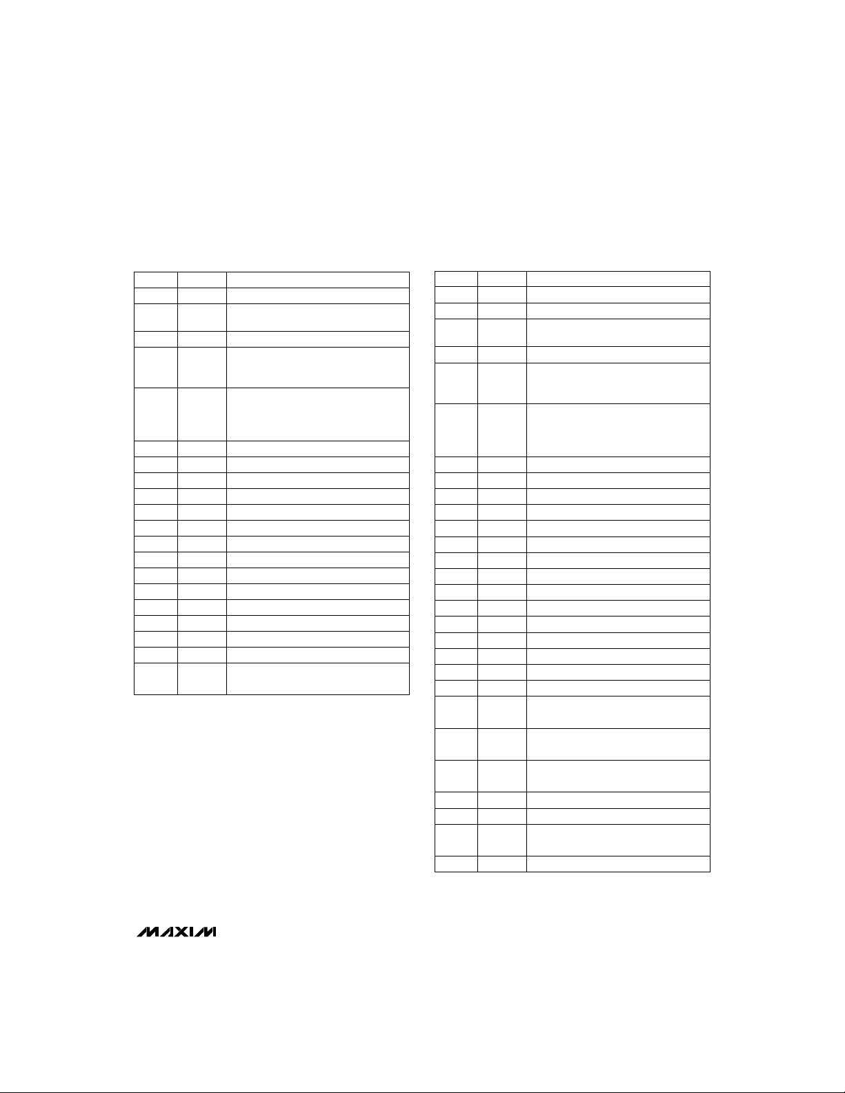
PART TEMP. RANGE PIN-PACKAGE INL (LSBs)
MX7534KN
MX7534JN 0°C to +70°C 20 Plastic DIP ±2
MX7534KCWP
MX7534JCWP 0°C to +70°C 20 SO ±2
MX7534KP 0°C to +70°C 20 PLCC ±1
MX7534JP 0°C to +70°C 20 PLCC ±2
MX7534J/D 0°C to +70°C Dice* ±2
MX7534BQ -25°C to +85°C 20 CERDIP ±1
MX7534AQ -25°C to +85°C 20 CERDIP ±2
MX7534BD
MX7534AD -25°C to +85°C 20 Ceramic SB ±2
MX7534KEWP -40°C to +85°C 20 SO ±1
MX7534JEWP -40°C to +85°C 20 SO ±2
MX7534TQ -55°C to +125°C 20 CERDIP ±1
MX7534SQ -55°C to +125°C 20 CERDIP ±2
MX7534TD -55°C to +125°C 20 Ceramic SB ±1
MX7534SD -55°C to +125°C 20 Ceramic SB ±2
Ordering Information continued at end of data sheet.
*
Dice are tested at +25°C, DC parameters only.
0°C to +70°C 20 Plastic DIP ±1
0°C to +70°C 20 SO ±1
-25°C to +85°C 20 Ceramic SB ±1
MX7534/MX7535
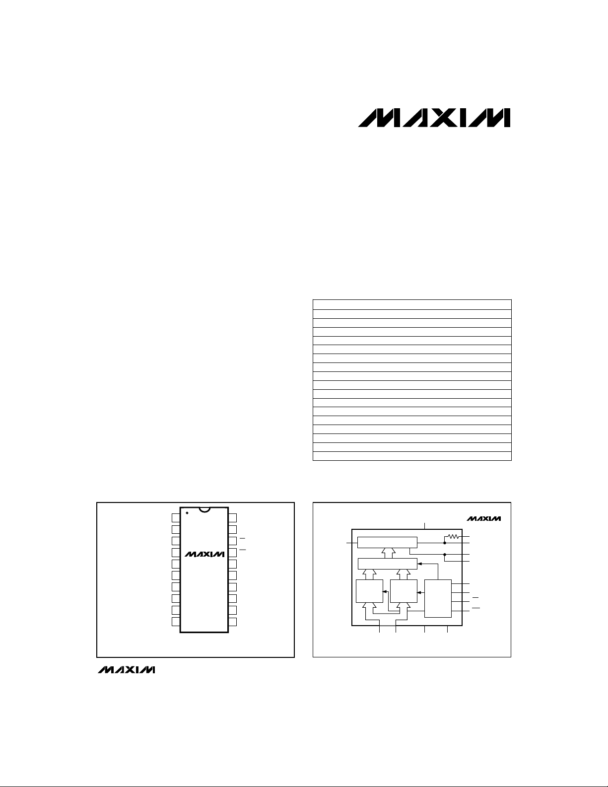
_________________Pin Configurations
_______________Functional Diagrams
TOP VIEW
REF
RFB
IOUT
AGNDS
AGNDF
DGND
D7
D6
D5
D4
DIP/SO/PLCC/Ceramic SB
MX7535 at end of data sheet.
________________________________________________________________
1
2
3
4
MX7534
5
6
7
8
9
10
20
V
SS
V
19
DD
18
CS
WR
17
A0
16
A1
15
D0
14
D1
13
12
D2
D3
11
1
REF
Functional diagrams continued at end of data sheet.
14-BIT DAC
14
DAC REGISTER
6
MS
INPUT
REGISTER
7–14
D7–D0 DGND V
V
DD
19
8
LS
INPUT
REGISTER
CONTROL
LOGIC
6
20
SS
Maxim Integrated Products
2
3
4
5
15
16
18
17
MX7534
RFB
IOUT
AGNDS
AGNOF
A1
A0
CS
WR
1
For free samples & the latest literature: http://www.maxim-ic.com, or phone 1-800-998-8800
Page 2
Microprocessor-Compatible,
14-Bit DACs
ABSOLUTE MAXIMUM RATINGS
VDDto DGND ............................................................-0.3V, +17V
to AGND.............................................................-15V, +0.3V
V
SS
REF to AGND (MX7534) ......................................................±25V
REFS to AGND (MX7535)....................................................±25V
REFF to AGND (MX7535) ....................................................±25V
RFB to AGND.......................................................................±25V
Digital Input Voltage to DGND.........................-0.3V, V
IOUT to DGND.................................................-0.3V, V
AGND to DGND...............................................-0.3V, V
Continuous Power Dissipation (T
20-Pin Plastic DIP (derate 11.11mW/°C above +70°C)....889mW
28-Pin Plastic DIP (derate 14.29mW/°C above +70°C)......1.14W
20-Pin SO (derate 10.00mW/°C above +70°C)..............800mW
28-Pin SO (derate 12.50mW/°C above +70°C).....................1W
20-Pin PLCC (derate 10.00mW/°C above +70°C) .........800mW
Stresses beyond those listed under “Absolute Maximum Ratings” may cause permanent damage to the device. These are stress ratings only, and functional
MX7534/MX7535
operation of the device at these or any other conditions beyond those indicated in the operational sections of the specifications is not implied. Exposure to
absolute maximum rating conditions for extended periods may affect device reliability.
= +70°C)
A
DD
DD
DD
+ 0.3V
+ 0.3V
+ 0.3V
ELECTRICAL CHARACTERISTICS
(VDD= +11.4V to +15.75V (Note 1), V
DC ACCURACY
Full-Scale Error
Gain Temperature Coefficient
(Note 2)
Output Leakage Current
REFERENCE INPUT
Reference Voltage Input
Resistance (Note 3)
DIGITAL INPUTS
Input High Voltage
Input Low Voltage V0.8
Input Leakage Current µA
Input Capacitance (Note 2)
= 10V, V
REF
INLRelative Accuracy
I
OUT
V
REF
INH
INL
IN
IOUT
MX753_K/B/T
MX753_J/A/S
Measured with internal RFB,
includes effects of leakage
current and gain TC
MX753_K/B/T
MX753_J/A/S
All digital
inputs at 0V
All digital
inputs at 0V,
VSS= 0V
Digital inputs
at 0V or V
= V
AGNDS
DD
28-Pin PLCC (derate 10.53mW/°C above +70°C) .........842mW
20-Pin CERDIP (derate 11.11mW/°C above +70°C)......889mW
28-Pin CERDIP (derate 16.67mW/°C above +70°C)........1.33W
20-Pin Ceramic SB
(derate 11.76mW/°C above +70°C).............................941mW
28-Pin Ceramic SB
(derate 20.00mW/°C above +70°C)................................1.6W
Operating Temperature Ranges
MX753_J/K............................................................0°C to +70°C
MX753_A/B........................................................-25°C to +85°C
MX753_EW_.......................................................-40°C to +85°C
MX753_S/T.......................................................-55°C to +125°C
Storage Temperature Range.............................-65°C to +150°C
Lead Temperature (soldering, 10sec).............................+300°C
= VSS= 0V, TA= T
CONDITIONS
MX753_K/B/T
MX753_J/A/S
TA= +25°C
MIN
MAX
MIN
MX753_J/K/A/B
MX753_S/T
to T
TA= T
to T
TA= +25°C
TA= T
MAX
MIN
to T
, unless otherwise noted.)
MAX
±1
±2
±4
±8
±0.5 ±2.5
±0.5 ±5
±5
±25
±150
±1
±10
UNITSMIN TYP MAXSYMBOLPARAMETER
ppm/°C
Bits14Resolution
LSB
LSB±1Guaranteed MonotonicDifferential Nonlinearity
LSB
nA
kΩ3.5 6 10R
V2.4V
pF7C
2 _______________________________________________________________________________________
Page 3
Microprocessor-Compatible,
14-Bit DACs
ELECTRICAL CHARACTERISTICS (continued)
(VDD= +11.4V to +15.75V (Note 1), V
POWER REQUIREMENTS
Positive Supply-Voltage Range
Negative Supply-Voltage Range
Positive Supply Current
Negative Supply Current
Note 1: Specifications are guaranteed for VDDof +11.4V to +15.75V. At VDD= +5V, device is still functional with degraded specifications.
Note 2: Guaranteed by design, not tested.
Note 3: Resistors have a typical -300ppm/°C tempco.
= 10V, V
REF
I
DD
SS
DD
SS
IOUT
For specific performance
For specific performance
Digital inputs at
V
INH
Digital inputs at 0V or V
or V
= V
AGNDS
INL
= VSS= 0V, TA= T
CONDITIONS
MX7534
MX7535
DD
MIN
to T
, unless otherwise noted.)
MAX
UNITSMIN TYP MAXSYMBOLPARAMETER
V11.4 15.75V
mV-200 -500V
3
mA
4
µA500I
AC PERFORMANCE CHARACTERISTICS (Note 4)
(VDD= +11.4V to +15.75V, V
= T
to T
T
A
MIN
Digital-to-Analog Glitch Impulse
Multiplying Feedthrough Error
(Note 5)
Power-Supply Rejection
Output Capacitance (IOUT Pin)
Output Noise Voltage Density
(10Hz–100kHz)
Note 4: These characteristics are included for design guidance only, and are not subject to test.
Note 5: Feedthrough can be further reduced by connecting the metal lid on the ceramic package to DGND.
, unless otherwise noted.)
MAX
REF
= 10V, V
C
OUT
= V
IOUT
AGND(VAGNDS
TA= +25°C, to 0.003% of full-scale range,
IOUT load = 100Ω
alternately loaded with all 1s and all 0s
Measured with V
IOUT loads = 100Ω
alternately loaded with all 1s and all 0s
V
= ±10V, 10kHz
REF
sine wave, DAC register
loaded with all 0s
∆VDD= ±5%
DAC register loaded with all 1s
DAC register loaded with all 0s
Measured between RFBand I
for MX7535) = VSS= 0V, output amplifier is AD544*,
CONDITIONS
13pF, DAC register
II
= 0V,
REF
13pF, DAC register
II
TA= +25°C
TA= T
TA= +25°C
TA= T
OUT
MIN
MIN
to T
to T
MAX
MAX
UNITSMIN TYP MAXSYMBOLPARAMETER
µs0.8 1.5Output Current Setting Time
nV-sec50
3
5
±0.01
±0.02
260
130
mVp-p
%/%
pF
nV/Hz15
MX7534/MX7535
* AD544 is an Analog Devices part.
_______________________________________________________________________________________ 3
Page 4
Microprocessor-Compatible,
14-Bit DACs
TIMING CHARACTERISTICS (MX7534)
(VDD= +11.4V to +15.75V, V
timing diagram.)
Address Valid to Write Setup Time
Address Valid to Write Hold Time
Data Setup Time
Data Hold Time
Chip-Select to Write-Setup Time
Chip-Select to Write-Hold Time
MX7534/MX7535
Write Pulse Width
TIMING CHARACTERISTICS (MX7535)
(VDD= +11.4V to +15.75V, V
timing diagram.)
CSMSB or CSLSB to WR Setup Time
CSMSB or CSLSB to WR Hold Time
LDAC Pulse Width
Write Pulse Width
Data-Setup Time
Data-Hold Time
REF
REF
= 10V, V
= 10V, V
IOUT
IOUT
= V
= V
= VSS= 0V, TA= T
AGND
1
2
TA= +25°C
t
TA= -25°C to +85°C
3
TA= -55°C to +125°C
TA= +25°C
TA= -25°C to +85°C
t
4
TA= -55°C to +125°C
t
5
t
6
TA= +25°C
t
TA= -25°C to +85°C
7
TA= -55°C to +125°C
= VSS= 0V, TA= T
AGNDS
1
2
TA= +25°C
t
TA= -25°C to +85°C
3
TA= -55°C to +125°C
TA= +25°C
t
TA= -25°C to +85°C
4
TA= -55°C to +125°C
TA= +25°C
t
TA= -25°C to +85°C
5
TA= -55°C to +125°C
TA= +25°C
t
TA= -25°C to +85°C
6
TA= -55°C to +125°C
to T
MIN
CONDITIONS
MIN
CONDITIONS
, unless otherwise noted. See Figure 1a for
MAX
60
70
80
20
20
30
0
0
170
200
240
to T
, unless otherwise noted. See Figure 1b for
MAX
170
200
240
170
200
240
140
160
180
20
20
30
UNITSMIN TYP MAXSYMBOLPARAMETER
ns0t
ns0t
ns
ns
ns
ns
ns
UNITSMIN TYP MAXSYMBOLPARAMETER
ns0t
ns0t
ns
ns
ns
ns
4 _______________________________________________________________________________________
Page 5
Microprocessor-Compatible,
14-Bit DACs
__________Pin Description (MX7534)
NAME FUNCTION
PIN
REF Reference Input to DAC
1
2 RFB
3 IOUT Current Output
4 AGNDS
5 AGNDF
6 DGND Digital Ground
7 D7 Data Bit 7
8 D6 Data Bit 6
9 D5 Data Bit 5 or Data Bit 13 (MSB)
10 D4 Data Bit 4 or Data Bit 12
11 D3 Data Bit 3 or Data Bit 11
12 D2 Data Bit 2 or Data Bit 10
13 D1 Data Bit 1 or Data Bit 9
14 D0 Data Bit 0 (LSB) or Data Bit 8
15 A1 Address Input 1
16 A0 Address Input 0
17
18
19 V
20 V
WR
Feedback Resistor. Used to close the
loop around an external op amp.
Analog Ground Sense. Reference
point for external circuitry. AGNDS
should carry minimum current.
Analog Ground Force. Carries current
from internal analog ground connections. AGNDS and AGNDF are tied
together internally.
Write Input. Active low.
Chip-Select Input. Active low.
CS
+12V to +15V Supply-Voltage Input
DD
Bias pin for high-temperature,
SS
low-leakage configuration
__________Pin Description (MX7535)
NAME FUNCTION
PIN
REFS Reference Voltage Sense
1
2 REFF
3 RFB
4
IOUT Current Output
5 AGNDS
6 AGNDF
7 DGND Digital Ground
8 D13 Data Bit 13 (MSB)
9 D12 Data Bit 12
10 D11 Data Bit 11
11 D10 Data Bit 10
12 D9 Data Bit 9
13 D8 Data Bit 8
14 D7 Data Bit 7
15 D6 Data Bit 6
16 D5 Data Bit 5
17 D4 Data Bit 4
18 D3 Data Bit 3
19 D2 Data Bit 2
20 D1 Data Bit 1
21 D0 Data Bit 0 (LSB)
22
CSMSB
23
LDAC
24
CSLSB
25
26 V
27 V
28 N.C.
Reference Voltage Force
Feedback Resistor. Used to close the
loop around an external op amp.
Analog Ground Sense. Reference
point for external circuitry. This pin
should carry minimum current.
Analog Ground Force. Carries current
from internal analog ground
connections. AGNDS and AGNDF
are tied together internally.
Chip-Select Most Significant Byte.
Active low.
Asynchronous Load DAC Input.
Active low.
Chip-Select Least Significant Byte.
Active low.
Write Input. Active low.
WR
+12V to +15V Supply-Voltage Input
DD
Bias pin for high-temperature,
SS
low-leakage configuration
No Connection. Not internally connected.
MX7534/MX7535
_______________________________________________________________________________________ 5
Page 6

Microprocessor-Compatible,
14-Bit DACs
A0,A1
DATA
t
1
t
5
CS
WR
t
7
t3t
t
2
4
t
6
MX7534/MX7535
NOTES:
1) ALL INPUT-SIGNAL RISE AND FALL TIMES ARE MEASURED FROM 10% TO 90%
OF +5V. t
= tF = 20ns.
R
2) TIMING MEASUREMENT REFERENCE LEVEL IS
Figure 1a. MX7534 Timing Diagram
_______________Detailed Description
Digital-to-Analog Section
The basic MX7534/MX7535 digital-to-analog converter
(DAC) circuit consists of a laser-trimmed, thin-film,
11-bit R-2R resistor array, a 3-bit segmented resistor
array, and NMOS current switches, as shown in Figure
2. The three MSBs are decoded to drive switches A–G
of the segmented array, and the remaining bits drive
switches S0–S10 of the R-2R array.
Binary weighted currents are switched to either AGNDF
or I
, depending on the status of each input bit. The
OUT
R-2R ladder current is one-eighth of the total reference
input current. The remaining seven-eighths of the current flows in the segmented resistors, dividing equally
among these seven resistors. The input resistance at
REF is constant; therefore, it can be driven by a voltage
or current source of positive or negative polarity.
The MX7534/MX7535 are optimized for unipolar output
operation (analog output from 0V to -V
bipolar operation (analog output from +V
possible with some added external components.
Figure 3 shows the equivalent circuit for the two DACs.
C
varies from about 90pF to 180pF, depending on
OUT
the digital code. R0denotes the DAC’S equivalent output resistance, which varies with the input code.
V
IH + VIL
2
), although
REF
to -V
REF
REF
t
5V
0V
5V
0V
5V
0V
5V
0V
1
CSMSB
CSLSB
LDAC
WR
DATA
NOTES:
1) ALL INPUT-SIGNAL RISE AND FALL TIMES ARE MEASURED FROM 10% TO 90%
OF +5V. t
2) TIMING MEASUREMENT REFERENCE LEVEL IS
3) IF LDAC IS ACTIVATED PRIOR TO THE RISING EDGE OF WR, THEN IT MUST
STAY LOW FOR t
t
2
t
4
t
6
t
5
= tF = 20ns.
R
OR LONGER AFTER WR GOES HIGH.
3
t
1 t
t
4
t
5
V
IH + VIL
2
Figure 1b. MX7535 Timing Diagram
,
N) is the Thevenin equivalent voltage generator
g(V
REF
due to the reference input voltage, V
REF
fer function of the R-2R ladder, N.
Digital Section
All digital inputs are both TTL and 5V CMOS logic compatible. The digital inputs are protected from electrostatic discharge (ESD) with typical input currents of less than 1nA.
To minimize power-supply currents, keep digital input voltages as close to 0V and 5V logic levels as possible.
__________Applications Information
Unipolar Operation (2-Quadrant
Figures 4a and 4b show the circuit diagram for unipolar
binary operation. With an AC input, the circuit performs
2-quadrant multiplication. The code table for Figure 4 is
given in Table 2.
Capacitor C1 provides phase compensation and helps
prevent overshoot and ringing when high-speed op
) is
amps are used. Note that the output polarity is the
inverse of the reference input.
Multiplication)
2
t
3
t
6
, and the trans-
5V
0V
5V
0V
5V
0V
5V
0V
6 _______________________________________________________________________________________
Page 7

REFS*
WR CS
Microprocessor-Compatible,
14-Bit DACs
RR
R
MX7534/MX7535
REFF*
Figure 2. Simplified Circuit Diagram
2R 2R
G F E D C B A S10 S9 S0
*NOTE: VALID FOR MX7535. IN MX7534, 0REFS AND 0REFF ARE REPLACED BY ONE PIN: REF.
2R 2R 2R 2R 2R 2R 2R
Zero-Offset Adjustment
(Figures 4a and 4b)
1) Load the DAC register with all 0s.
2) Adjust the offset of amplifier A1 so that V0(see figure) is at a minimum (i.e., ≤ 30µV).
Gain Adjustment
(Figures 4a and 4b)
1) Load the DAC register with all 1s.
2) Trim potentiometer R1 so that V
OUT
= -V
IN
16383
(
16384
)
In fixed-reference applications, adjust full scale by
omitting R1 and R2 and trimming the reference voltage
magnitude. In many applications, the excellent Gain
Tempco and Gain Error specifications eliminate the
need for gain adjustment. However, if trims are
required and the DAC is to operate over a wide temperature range, use low-tempco (>300ppm/°C) resistors.
Bipolar Operation
(4-Quadrant Multiplication)
Bipolar or 4-quadrant operation is shown in Figures 5a
and 5b. This configuration provides for offset binary
coding. Table 4 shows DAC codes and the corresponding analog outputs for Figures 5a and 5b. With
the DAC loaded to 10 0000 0000 0000, either adjust R1
for V
R5 and R6 for V
= 0V, or omit R1 and R2 and adjust the ratio of
OUT
= 0V. Adjust the amplitude of V
OUT
or vary the value of R7 for full-scale trimming.
Resistors R5, R6, and R7 must be matched to 0.003%.
Mismatch of R5 and R6 causes both offset and fullscale errors. For wide temperature range operation,
use resistors of the same material so that their temperature coefficients match and track.
2R2R
R/4
R
O
+
g(V
, N) C
REF
–
Figure 3. Equivalent Analog Output Circuit
I
LEAKAGE
OUT
Table 1. MX7534 Logic States
A1 A2 FUNCTION
X 1 X X Device not selected (Note 1)
1 X X X No data transfer
0000
0001
0010
IN
0011
Note 1: X = Don’t Care.
Note 2: When A1 = 0 and A0 = 0, all DAC registers are trans-
parent. By placing all 0s or all 1s on the data inputs, the
user can load the DAC to zero or full-scale output in
one write operation. This simplifies system calibration.
DAC loaded directly from
Data Bus (Note 2)
MS Input Register loaded
from Data Bus
LS Input Register loaded
from Data Bus
DAC Register loaded from
Input Registers
R/4
RFB
IOUT
AGNDS
AGNDF
RFB
IOUT
AGNDS
AGNDF
_______________________________________________________________________________________ 7
Page 8

Microprocessor-Compatible,
14-Bit DACs
R1
V
DD
16
15
18
17
100Ω
REF RFB
D7–D0
7–14
INPUT
DATA
MX7534
DGND
620
V
2191
AGNDF
SS
33Ω
IOUT
AGNDS
R2
3
4
5
C1
33pF
A1
ANALOG
GROUND
V
IN
A0
A1
CS
WR
Figure 4a. Unipolar Binary Operation
MX7534/MX7535
Grounding Considerations
Since IOUT and the output amplifier noninverting input
are sensitive to offset voltages, connect nodes that
must be grounded directly to a single-point ground
through a separate, very-low-resistance path. Note that
the output currents at IOUT and AGNDF vary with input
code and create code-dependent error if these terminals are connected to ground (or a virtual ground)
through a resistive path.
To obtain high accuracy, it is important to use a proper
grounding technique. The two AGND pins (AGNDF‚
AGNDS) provide flexibility in this respect. In Figures 4a
and 4b, AGNDS and AGNDF are shorted together
externally and an extra op amp, A2, is not used.
Voltage-drops due to bond-wire resistance are not
compensated for in this circuit; this could create a linearity error of approximately 0.1LSB due to bond-wire
resistance alone. This can be eliminated by using the
circuits shown in Figures 6a and 6b, where A2 maintains AGNDS at signal ground potential. By using
force/sense techniques, all switch contacts on the DAC
are kept at exactly the same potential, and any error
caused by bond-wire resistance is eliminated.
Figure 7 shows a remote voltage reference driving the
MX7535. Op amps A2 and A3 compensate for voltage
drops along the reference input line and analog
ground line.
Figure 8 shows a printed circuit board (PCB) layout with
a single output amplifier for the MX7534. The input to
REF (Pin 1) is shielded to reduce AC feedthrough, while
the digital inputs are shielded to minimize digital
R1
20Ω
V
IN
REFF
REFS
V
INPUT
DATA
DD
MX7535
DGNDD13–DO
727
23
LDAC
22
V
O
CSMSB
25
WR
24
CSLSB
8–21
Figure 4b. Unipolar Binary Operation
RFB
V
32261
AGNDF
SS
10Ω
IOUT
AGNDS
R2
4
5
6
C1
33pF
A1
ANALOG
GROUND
V
O
Table 2. Unipolar Binary Code Table
BINARY NUMBER IN
DAC REGISTER
MSB LSB
11 1111 1111 1111
10 0000 0000 0000
00 0000 0000 0001
00 0000 0000 0000
feedthrough. The traces connecting IOUT and AGNDS
to the inverting and noninverting op amp inputs are
kept as short as possible. Gain trim components, R3
and R4, are omitted.
Zero-Offset Adjustment
1) Load DAC register with all 0s.
2) Adjust offset of amplifier A2 for minimum potential at
AGNDS. This potential should be ≤30µV with respect
to signal ground.
3) Adjust A1’s offset so that V
(i.e., ≤30µV).
ANALOG OUTPUT
(V
OUT)
16383
-V
IN
(
)
16384
8192
-V
-V
0V
IN
(
IN
(
= - 1V
)
16384 2
1
)
16384
IN
(Figures 6a and 6b)
is at a minimum
OUT
8 _______________________________________________________________________________________
Page 9

Microprocessor-Compatible,
CSMSB CSLSB LDAC W R
14-Bit DACs
V
IN
16
A0
15
A1
18
CS
17
WR
R1
100Ω
REF RFB
7–14
INPUT
DATA
V
MX7534
DD
DGNDD7–D0
620
AGNDF
V
SS
2191
R2, 33Ω
IOUT
AGNDS
5
3
4
C1
33pF
A1
+
ANALOG
GROUND
R6
20k
R5 10k
R8, 5k,10%
R7
20k
A2
+
V
O
Figure 5a. Bipolar Operation
Gain Adjustment
(Figures 6a and 6b)
1) Load DAC register with all 1s.
2) Trim potentiometer R3 so that V
OUT
= -
16383
(
16384
V
IN
)
Low-Leakage Configuration
Leakage current in the DAC flowing into the I
OUT
line
can cause gain, linearity, and offset errors. Leakage is
worse at high temperatures.
Negatively bias VSSfor a high-temperature, low-leakage
configuration.
Dynamic Considerations
In static or DC applications, the output amplifier’s AC
characteristics are not critical. In higher-speed applications, where either the reference input is an AC signal
or the DAC output must quickly settle to a new programmed value, the output op amp’s AC parameters
must be considered.
Another error source in dynamic applications is the parasitic signal coupling from the REF terminal to I
OUT
This is normally a function of board layout and lead-tolead package capacitance. Signals can also be injected into the DAC outputs when the digital inputs are
switched. This digital feedthrough depends on circuitboard layout and on-chip capacitive coupling. Minimize
layout-induced feedthrough with guard traces between
digital inputs, REF, and DAC outputs.
V
IN
R2 10Ω
V
DD
3
261
AGNDF
DGNDD13–D0
V
SS
7
27
IOUT
AGNDS
6
C1
33pF
4
+
5
ANALOG
GROUND
R6
20k
R5
10k
A1
R8, 5k,10%
LDAC
CSMSB
CSLSB
WR
R1
20Ω
2
REFF REFS RFB
23
22
25
24
8–21
INPUT
DATA
MX7535
Figure 5b. Bipolar Operation
Table 3. MX7535 Logic States
FUNCTION
0 1 1 0 Load MS Input Register
1 0 1 0 Load LS Input Register
0010
110X
0000
Load LS and MS Input
Registers
Load DAC Register
from Input Register
All registers are
transparent.
1 1 1 X No operation
X X 1 1 No operation
Note: X = Don’t Care.
Table 4. Offset Binary Bipolar Code Table
.
BINARY NUMBER IN
DAC REGISTER
MSB LSB
11 1111 1111 1111
10 0000 0000 0001
10 0000 0000 0000
01 1111 1111 1111
00 0000 0000 0000
Analog Output
(V
8191
+V
IN
(
8192
+V
IN
(1)
8192
0
-V
IN
(1)
8192
8192
-V
IN
(
8192
+
OUT)
)
= -V
)
MX7534/MX7535
R7
20k
A2
V
O
IN
_______________________________________________________________________________________ 9
Page 10

Microprocessor-Compatible,
14-Bit DACs
V
DD
R3
100Ω
V
REF RFB
V
IN
MX7534/MX7535
NOTE: CONTROL INPUTS OMITTED FOR CLARITY.
7–14
INPUT
DATA
MX7534
DGNDD7–D0
Figure 6a. Unipolar Binary Operation with Forced Ground
Table 5. Amplifier Performance Comparisons
OP AMP
MAX400 10µV 2nA 0.3µV/°C 50µs
Maxim OP07 25µV 2nA 0.6µV/°C 50µs
AD554L* 500µV 25pA 5µV/°C 5µs
HA2620* 4mV 35nA 20µV/°C 0.8µs
* AD544L is an Analog Devices part; HA2620 is a Harris Semiconductor part.
191
2
DD
AGNDF
V
SS
620
R4
33Ω
3
IOUT
AGNDS
+
4
5
INPUT OFFSET
VOLTAGE (VOS)
C1
33pF
A1
R
V
L
O
A2
+
SIGNAL
GROUND
INPUT BIAS
CURRENT (IB)
V
DD
R2
C1
10Ω
IOUT
33pF
A1
4
+
5
6
ANALOG
GROUND
A2
+
R
L
SIGNAL
GROUND
V
O
R1
20Ω
REFF REFS RFB
VOLTAGE
REFERENCE
NOTE: CONTROL INPUTS OMITTED FOR CLARITY.
8–21
MX7535
INPUT
DATA
32621
V
DD
AGNDS
AGNDF
DGNDD13–D0
V
SS
7
27
Figure 6b. Unipolar Binary Operation with Forced Ground for
Remote Load
OFFSET VOLTAGE
DRIFT (TC VOS)
SETTLING
TO 0.003% FS
Compensation
A compensation capacitor, C1, may be needed when
the DAC is used with a high-speed output amplifier.
The capacitor cancels the pole formed by the DAC’s
output capacitance and internal feedback resistance.
Its value depends on the type of op amp used, but typical values range from 10pF to 33pF. Too small a value
causes output ringing, while excess capacitance overdamps the output. Minimize C1’s size and improve output settling performance by keeping the PC board
trace as short as possible and stray capacitance at
I
as small as possible.
OUT
Bypassing
Place a 1µF bypass capacitor, in parallel with a 0.01µF
ceramic capacitor, as close to the DAC’s VDDand GND
pins as possible. Use a 1µF tantalum bypass capacitor
to optimize high-frequency noise rejection. Place a
The MX7534/MX7535 have high-impedance digital
inputs. To minimize noise pickup, connect them to
either V
or GND terminals when not in use. Connect
DD
active inputs to VDDor GND through high-value resistors (1MΩ) to prevent static charge accumulation if
these pins are left floating, as might be the case when
a circuit card is left unconnected.
Op-Amp Selection
Input offset voltage (VOS), input bias current (IB), and
offset voltage drift (TC VOS) are three key parameters in
determining the choice of a suitable amplifier. To maintain specified accuracy with V
REF
be less than 30µV and IBshould be less than 2nA.
Open-loop gain should be greater than 340,000.
Maxim’s MAX400 has low VOS(10µV max), low I
(2nA), and low TC VOS(0.3µV/°C max). This op amp
can be used without requiring any adjustments. For
4.7µF decoupling capacitor at VSSto minimize the DAC
output leakage current.
10 ______________________________________________________________________________________
of 10V, VOSshould
B
Page 11

Microprocessor-Compatible,
14-Bit DACs
MX7534/MX7535
V+
V-
V
DATA
MX7535
DGNDD13–D0
DD
32261
V
DD
IOUT
AGNDS
AGNDF
V
SS
7
27
C1
33pF
4
A1
+
5
6
V
0
R
L
OUTPUT
C1 LOCATION
V
SS
V
DD
A2
+
REFF REFS RFB
8–21
INPUT
PIN 1 AD544*
REF
PIN 1 MX7534
A3
+
NOTE: CONTROL INPUTS OMITTED FOR CLARITY.
Figure 7. Driving the MX7535 with a Remote Voltage Reference
medium-frequency applications, the OP27 is recommended. For higher-frequency applications, the HA2620 is recommended. However, these op amps
require external offset adjustment (Table 5).
________Microprocessor Interfacing
8086 with MX7535
The MX7534/MX7535 interface to both 8-bit and 16-bit
processors. Figure 9a shows the 8086 16-bit processor
interfacing to a single MX7535. In this setup, the doublebuffering feature of the DAC is not used. AD0–AD13 of
the 16-bit data bus are connected to the DAC data bus
(D0–D13). The 14-bit word is written to the DAC in one
MOV instruction, and the analog output responds immediately. In this example, the DAC address is D000. Table
6a shows a software routine for Figure 9a.
In a multiple DAC system, the double buffering of the
DAC chips allows the user to simultaneously update all
DACs. In Figure 10, a 14-bit word is loaded to each of
the DAC’s input registers in sequence. Then, with one
instruction to the appropriate address, CS4 (i.e., LDAC)
is brought low, updating all the DACs simultaneously.
8086 with MX7534
Figure 9b shows an interface circuit to a 16-bit microprocessor. The bottom 8 bits (AD0–AD7) of the 16-bit
data bus are connected to the DAC data bus. The
AGND
DGND
NOTE:
LAYOUT IS FOR DOUBLE-SIDED
PCB. BOLD LINE INDICATES
TRACK ON COMPONENT SIDE.
*AD544 IS AN ANALOG DEVICES PART.
Figure 8. Suggested Layout for MX7534 Incorporating Output
Amplifier
14-bit word is loaded in two bytes, using the MOV
instruction. A further MOV loads the DAC register and
causes the analog data to appear at the converter output. For the example given here, the appropriate DAC
register addresses are D002, D004, and D006. Table
6b shows the program for loading the DAC.
8085A with MX7534
A typical interface circuit is shown in Figure 9c. The
DAC is treated as four memory locations addressed by
A0 and A1. In standard operation, three of these memory locations are used. Table 6c shows a sample program for loading the DAC with a 14-bit word. The
MX7534 has address locations 3000–3003.
The six MSBs are written into location 3001, and eight
LSBs are written to 3002. Then, with a write instruction to
3003, the full 14-bit word is loaded to the DAC register.
______________________________________________________________________________________ 11
Page 12

Microprocessor-Compatible,
14-Bit DACs
MC68000 with MX7535
Figure 11a shows an interface diagram. The following
routine writes data to the DAC input registers and then
outputs the data via the DAC register:
01000 MOVE.W #W,D0 DAC data, W, loaded
MOVE.W D0,$E000 Data W transferred
MOVE.B #228,D7 Control returned to the
TRAP #14 Monitor Program
Figure 11b shows the MC68000 interface diagram. The
MX7534/MX7535
following routine writes data to the DAC input registers
and then outputs the data via the DAC register:
.A2 E003 Address Register 2
01000 MOVE.W #W,D0 DAC data, W, loaded
MOVEP.W D0,$0000
MOVE.W D0,$E006 This instruction provides
MOVE.B #228,D7 Control returned to the
TRAP #14 Monitor Program
Since this interfacing system uses only the lower half of
the data bus, it is also suitable for use with the
MC68008, which provides the user with an 8-bit data
bus instead of the MC68000’s 16-bit bus.
into Data Register 0.
between D0 and DAC
Register.
System.
MC68000 with MX7534
loaded with E003.
into Data Register 0.
(A2)
Data W transferred
between D0 and the
DAC’s Input Register.
High-ordered byte transferred first. Memory
address specified using
the address register
indirect plus displacement addressing mode.
Address used here
(E003) is odd, so data is
transferred on the loworder half of the data
bus (D0–D7).
appropriate signals to
transfer data W from
the DAC Input Register
to the DAC Register,
which controls the R-2R
ladder switches.
System.
ADDRESS BUS
16-BIT
ALE
LATCH
8086
WR
AD0–AD15
*SOME CIRCUITRY OMITTED FOR CLARITY
Figure 9a. MX7535—8086 Interface Circuit
16-BIT
ALE
LATCH
8086
WR
AD0–AD15
*SOME CIRCUITRY OMITTED FOR CLARITY
Figure 9b. MX7534—8086 Interface Circuit
A8–A15
LATCH
AE
8085A
WR
AD0–AD7
*SOME CIRCUITRY OMITTED FOR CLARITY
Figure 9c. MX7534—8085A Interface Circuit
ADDRESS
DECODE
DATA BUS
ADDRESS BUS
ADDRESS
DECODE
DATA BUS
ADDRESS
DECODE
DATA BUS
AD13
AD0
ADDRESS BUS
ADDRESS BUS
CSMSB
CSLSB
LDAC
MX7535*
WR
D0–D13
A2
A1 A0
CS
MX7534*
WR
D0–D7
A1 A0
CS
MX7534*
WR
D0–D7
A1
12 ______________________________________________________________________________________
Page 13

Microprocessor-Compatible,
14-Bit DACs
Table 6a. Sample Program for Loading the MX7535
ASSUME DS:DACLOAD,CS:DACLOAD
DACLOAD SEGMENT AT 000
00
02
04
07
0B
0E
8CC9
8ED9
BF00D0
C705“YZWX”
EA0000
00FF
MOV CX,CS
MOVDS,CX
MOVDI,#D000
MOV MEM,#YZWX
:DEFINE DATA SEGMENT REGISTER EQUAL
:TO CODE SEGMENT REGISTER
:LOAD DI WITH D000
:DAC LOADED WITH WXYZ
:CONTROL IS RETURNED TO THE MONITOR PROGRAM
Table 6b. Sample Program for Loading the MX7534 from 8086
ASSUME DS:DACLOAD,CS:DACLOAD
DACLOAD SEGMENT AT 000
00
02
04
07
0A
0B
0C
0F
10
11
14
8CC9
8ED9
BF02D0
C605“MS”
47
47
C605“LS”
47
47
C60500
EA0000
MOV CX,CS
MOVDS,CX
MOVDI.#D002
MOV MEM,#“MS”
INC DI
INC DI
MOV MEM,#“LS”
INC DI
INC DI
MOV MEM,#00
JMP MEM
:DEFINE DATA SEGMENT REGISTER EQUAL
:TO CODE SEGMENT REGISTER
:LOAD DI WITH D002
:DAC LOADED WITH “MS”
:LS INPUT REGISTER LOADED WITH “LS”
:CONTENT OF INPUT REGISTERS ARE LOADED TO THE DAC REGISTER
:CONTROL IS RETURNED TO THE MONITOR PROGRAM
Table 6c. Sample Program for Loading
the MX7534 from 8085A
2000
26
01
30
02
2E
03
01
04
3E
05
“MS”
06
77
07
2C
08
3E
09
“LS”
0A
77
0B
2C
0C
77
200D
CF
Figure 12a is an interface circuit for the Z80, using the
MX7535. This is an example of an 8-bit processor interface for these DACs. Figure 12b shows the schematic
for the MX7534.
MVIH,#30
MVIL,#01
MVIA,#“MS”
MOV M,A
INR L
MVI A#“LS”
MOV M,A
INR L
MOV M,A
RST I
Z80 with MX7534/MX7535
Figure 13a shows an interface circuit that enables the
MX7534 to be programmed using the MC6809 8-bit
microprocessor. Use the 16-bit D accumulator to simplify
data transfer. The two key processor instructions are:
LDD Load D accumulator from memory
STD Store D accumulator to memory
Figure 13b shows an interface diagram for the MC6502
using the MX7534.
________________Digital Feedthrough
In the interface diagrams shown in Figures 9–13, the
digital inputs of the DAC are directly connected to the
microprocessor bus. Even when the device is not
selected, activity on the bus can feed through on the
DAC output through package capacitance and appear
as noise. To minimize noise, isolate the DACs from the
digital bus, as shown in Figures 14a and 14b.
MX7534/MX7535
MC6809 with MX7534
MC6502 with MX7534
______________________________________________________________________________________ 13
Page 14

Microprocessor-Compatible,
14-Bit DACs
ADDRESS BUS
16-BIT
ALE
LATCH
8086
WR
AD0–AD15
MX7534/MX7535
ADDRESS
DECODE
CS4
DATA BUS
CSMSB
CS1
CS3
CS2
CSLSB
LDAC
WR
MX7535*
D0–D13
CSMSB
CSLSB
LDAC
WR
MX7535*
D0–D13
CSMSB
CSLSB
LDAC
WR
MX7535*
*SOME CIRCUITRY OMITTED FOR CLARITY
D0–D13
Figure 10. MX7535—8086 Interface: Multiple DAC Systems
A1–A23
AS
MC68000
DTACK
R/W
D0–D15
*SOME CIRCUITRY OMITTED FOR CLARITY
ADDRESS BUS
ADDRESS
DECODE
DATA BUS
CSMSB
CSLSB
LDAC
MX7535*
WR
D0–D13
Figure 11a. MX7535—MC68000 Interface
A1–A23
AS
MC68000
DTACK
R/W
D0–D7
ADDRESS
DECODE
ADDRESS BUS
DATA BUS
CS
MX7534*
WR
D0–D7
A2A1
A1A0
*SOME CIRCUITRY OMITTED FOR CLARITY
Figure 11b. MX7534—MC68000 Interface
14 ______________________________________________________________________________________
Page 15

A0–A15
ADDRESS BUS
Microprocessor-Compatible,
14-Bit DACs
A0–A15
ADDRESS BUS
MX7534/MX7535
MREQ
ADDRESS
DECODE
Z80
WR
D8–D7
*SOME CIRCUITRY OMITTED FOR CLARITY
DATA BUS
CSLSB
CSMSB
LDAC
MX7535*
WR
D8–D13
D0–D7
Figure 12a. MX7535—Z80 Interface
A0–A15
R/W
Q
E
ADDRESS BUS
ADDRESS
DECODE
A0 A1
CS
MX7534*
WR
MC6809
D0–D7
*SOME CIRCUITRY OMITTED FOR CLARITY
DATA BUS
D0–D7
Figure 13a. MX7534—MC6809 Interface Circuit
A0 A1
ADDRESS
DECODE
EN
QUAD LATCH
EN
QUAD LATCH
EN
QUAD LATCH
A1
A0
WR
MX7534*
D0–D7
CS
A0–A15
WR
MICRO-
PROCESSOR
SYSTEM
D0–D7
*SOME CIRCUITRY OMITTED FOR CLARITY
Figure 14a. MX7534—Interface Circuit Using Latches to
Minimize Digital Feedthrough
MREQ
ADDRESS
DECODE
Z80
WR
D0–D7
*SOME CIRCUITRY OMITTED FOR CLARITY
DATA BUS
A0 A1
CS
MX7534*
WR
D0–D7
Figure 12b. MX7534—Z80 Interface
A0–A15
R/W
6502
∅2
D0–D7
*SOME CIRCUITRY OMITTED FOR CLARITY
ADDRESS BUS
ADDRESS BUS
ADDRESS
DECODE
DATA BUS
A0 A1
CS
MX7534*
WR
D0–D7
Figure 13b. MX7534—6502 Interface
A0–A15
MICRO-
PROCESSOR
SYSTEM
WR
D0–D15
*SOME CIRCUITRY OMITTED FOR CLARITY
ADDRESS
DECODE
EN
16-BIT
LATCH
CSMSB
CSLSB
LDAC
WR
MX7535*
D0–D13
Figure 14b. MX7535—Interface Circuit Using Latches to
Minimize Digital Feedthrough
______________________________________________________________________________________ 15
Page 16

Microprocessor-Compatible,
14-Bit DACs
___Functional Diagrams (continued)
V
DD
26
1
REFS
2
REFF
MX7534/MX7535
14-BIT DAC
14
DAC REGISTER
6
MS
INPUT
REGISTER
8–21
D13–D0 DGND V
8
LS
INPUT
REGISTER
7
MX7535
3
RFB
4
IOUT
5
AGNDS
6
AGNDF
23
LDAC
24
CSLSB
22
CSMSB
25
WR
27
SS
_Ordering Information (continued)
MX7535KN
*
Dice are tested at +25°C, DC parameters only.
INL (LSBs)PIN PACKAGETEMP. RANGEPART
_____Pin Configurations (continued)
TOP VIEW
N.C.
REFS
1
REFF
2
RFB
3
IOUT
4
AGNDS
5
AGNDF
DGND
(MSB) D13
D12
D11
D10
D9
D8
D7
±128 Plastic DIP0°C to +70°C
±228 Plastic DIP0°C to +70°CMX7535JN
DIP/SO/PLCC/Ceramic SB
MX7535
6
7
8
9
10
11
12
13
14
±128 Wide SO0°C to +70°CMX7535KCWI
±228 Wide SO0°C to +70°CMX7535JCWI
±128 PLCC0°C to +70°CMX7535KP
±228 PLCC0°C to +70°CMX7535JP
±2Dice*0°C to +70°CMX7535J/D
±128 CERDIP-25°C to +85°CMX7535BQ
±228 CERDIP-25°C to +85°CMX7535AQ
±128 Ceramic SB-25°C to +85°CMX7535BD
±228 Ceramic SB-25°C to +85°CMX7535AD
±128 Wide SO-40°C to +85°CMX7535KEWI
±228 Wide SO-40°C to +85°CMX7535JEWI
±128 CERDIP-55°C to +125°CMX7535TQ
±228 CERDIP-55°C to +125°CMX7535SQ
±128 Ceramic SB-55°C to +125°CMX7535TD
±228 Ceramic SB-55°C to +125°CMX7535SD
28
27
26
25
24
23
22
21
20
19
18
17
16
15
V
SS
V
DD
WR
CSLSB
LDAC
CSMSB
D0 (LSB)
D1
D2
D3
D4
D5
D6
Maxim cannot assume responsibility for use of any circuitry other than circuitry entirely embodied in a Maxim product. No circuit patent licenses are
implied. Maxim reserves the right to change the circuitry and specifications without notice at any time.
16
__________________Maxim Integrated Products, 120 San Gabriel Drive, Sunnyvale, CA 94086 (408) 737-7600
© 1996 Maxim Integrated Products Printed USA is a registered trademark of Maxim Integrated Products.
 Loading...