

Page 1
General Description
The MAXQ7670 is a highly integrated solution for measuring multiple analog signals and outputting the results
on a control area network (CAN) bus. The device operates from a single 5V supply and incorporates a highperformance, 16-bit reduced instruction set computing
(RISC) core, a SAR ADC, and a CAN 2.0B controller,
supporting transfer rates up to 1Mbps. The 10-bit SAR
ADC includes an amplifier with programmable gains of
1V/V or 16V/V, 8 input channels, and conversion rates up
to 250ksps. The eight single-ended ADC inputs can be
configured as four unipolar or bipolar, fully differential
inputs. For single-supply operation, the external 5V supply powers the digital I/Os and two separate integrated
linear regulators that supply the 2.5V digital core and the
3.3V analog circuitry. Each supply rail has a dedicated
power-supply supervisor that provides brownout detection and power-on reset (POR) functions. The 16-bit RISC
microcontroller (µC) includes 64KB (32K x 16) of nonvolatile program/data flash and 2KB (1K x 16) of data
RAM. Other features of the MAXQ7670 include a 4-wire
SPI™ interface, a JTAG interface for in-system programming and debugging, an integrated 15MHz RC oscillator, external crystal oscillator support, a timer/counter
with pulse-width modulation (PWM) capability, and seven
GPIO pins with interrupt and wake-up capability.
The system-on-a-chip (SoC) MAXQ7670 is a µC-based,
smart data acquisition system. As a member of the
MAXQ®family of 16-bit, RISC µCs, the MAXQ7670 is
ideal for low-cost, low-power, embedded-applications
such as automotive, industrial controls, and building
automation. The flexible, modular architecture used in
the MAXQ µCs allows development of targeted products for specific applications with minimal effort.
The MAXQ7670 is available in a 40-pin, 5mm x 5mm
TQFN package, and is specified to operate over the -40°C
to +125°C automotive temperature range.
Applications
Automotive Steering Angle and Torque Sensors
CAN-Based Automotive Sensor Applications
Industrial Control
Building Automation
Features
♦ High-Performance, Low-Power, 16-Bit RISC Core
0.166MHz to 16MHz Operation, Approaching
1MIPs/MHz
Low Power (< 1mA/MIPS, V
DVDD
= +2.5V)
16-Bit Instruction Word, 16-Bit Data Bus
33 Instructions, Most Require Only One Clock
Cycle
16-Level Hardware Stack
16 x 16-Bit, General-Purpose Working Registers
Three Independent Data Pointers with AutoIncrement/Decrement
Low-Power, Divide-by-256, Power-Management
Modes (PMM) and Stop Mode
♦ Program and Data Memory
64KB Internal Nonvolatile Program/Data Flash
2KB Internal Data RAM
♦ SAR ADC
8 Single-Ended/4 Differential Channels,
10-Bit Resolution with No Missing Codes
PGA Gain = 1V/V or 16V/V
250ksps (150.9ksps with PGA Gain = 16V/V)
♦ Timer/Digital I/O Peripherals
CAN 2.0B Controller (15 Message Centers)
Serial Peripheral Interface (SPI)
JTAG Interface (Extensive Debug and Emulation
Support)
Single 16-Bit/Dual 8-Bit Timer/PWM
Seven General-Purpose, Digital I/O Pins with
External Interrupt/Wake-Up Features
♦ Oscillator/Clock Module
Internal Oscillator Supports External Crystal
(8MHz or 16MHz)
Integrated 15MHz RC Oscillator
External Clock Source Operation
Programmable Watchdog Timer
♦ Power-Management Module
Power-On Reset
Power-Supply Supervisor/Brownout Detection
Integrated +2.5V and +3.3V Linear Regulators
MAXQ7670
Microcontroller with 10-Bit ADC,
PGA, 64KB Flash, and CAN Interface
________________________________________________________________
Maxim Integrated Products
1
19-4384; Rev 0; 11/08
For pricing, delivery, and ordering information, please contact Maxim Direct at 1-888-629-4642,
or visit Maxim’s website at www.maxim-ic.com.
Typical Application Circuit and Pin Configuration appear at
end of data sheet.
SPI is a trademark of Motorola, Inc.
MAXQ is a registered trademark of Maxim Integrated Products, Inc.
Ordering Information
PART TEMP RANGE PIN-PACKAGE
MAXQ7670ATL+
40 TQFN-EP*
+
Denotes a lead-free/RoHS-compliant package.
*
EP = Exposed pad.
Note: Some revisions of this device may incorporate deviations from published specifications known as errata. Multiple revisions of
any device may be simultaneously available through various sales channels. For information about device errata, go to:
http://www.maxim-ic.com/errata
.
-40°C to +125°C
Page 2
MAXQ7670
Microcontroller with 10-Bit ADC,
PGA, 64KB Flash, and CAN Interface
2 _______________________________________________________________________________________
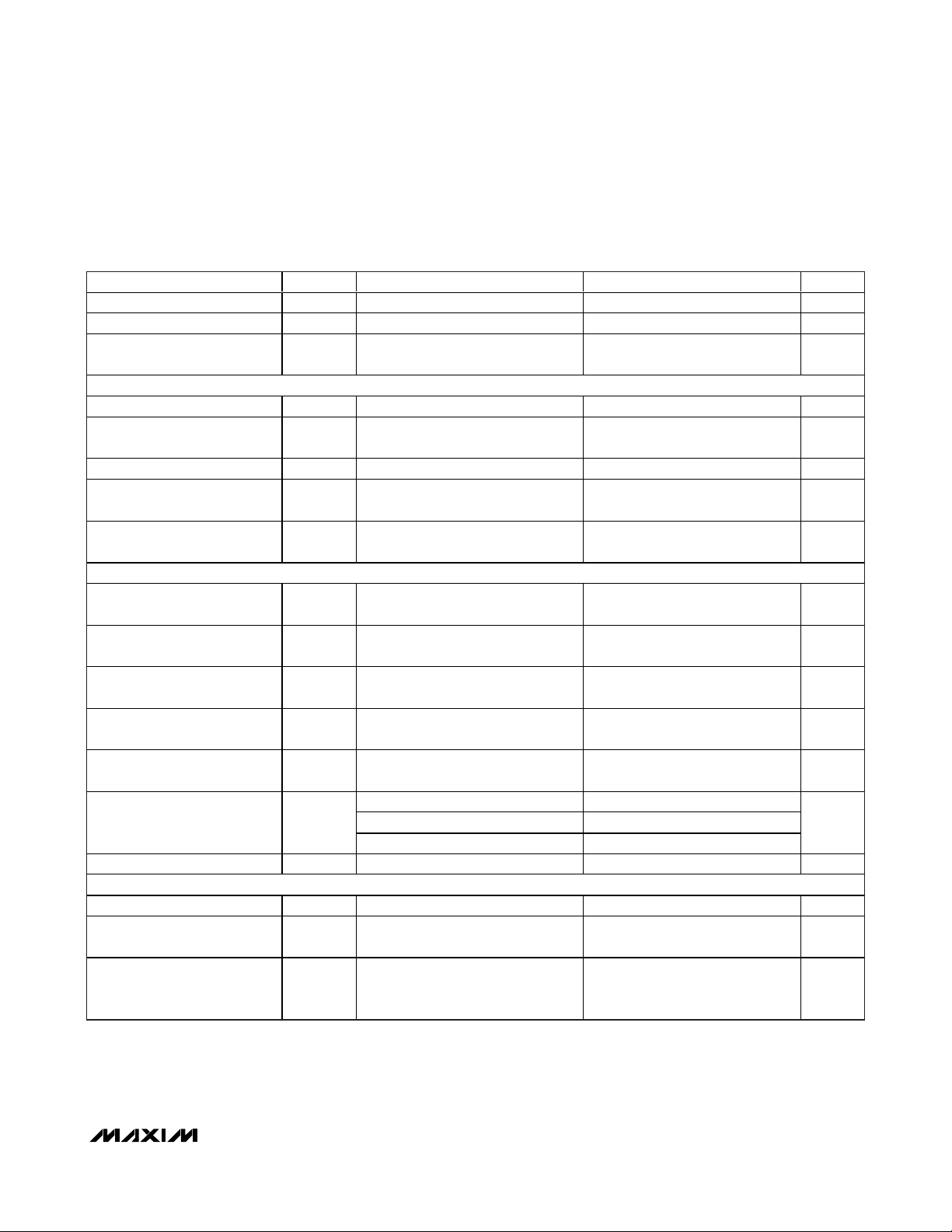
ABSOLUTE MAXIMUM RATINGS
ELECTRICAL CHARACTERISTICS
(V
DVDDIO
= +5.0V, V
AVDD
= +3.3V, V
DVDD
= +2.5V, V
REFADC
= +3.3V, system clock = 16MHz. TA= T
MIN
to T
MAX
, unless otherwise
noted. Typical values are at T
A
= +25°C.) (Note 1)
Stresses beyond those listed under “Absolute Maximum Ratings” may cause permanent damage to the device. These are stress ratings only, and functional
operation of the device at these or any other conditions beyond those indicated in the operational sections of the specifications is not implied. Exposure to
absolute maximum rating conditions for extended periods may affect device reliability.
DVDD to DGND ........................................................-0.3V to +3V
DVDDIO to GNDIO ................................................-0.3V to +5.5V
AVDD to AGND ........................................................-0.3V to +4V
DGND to GNDIO. ..................................................-0.3V to +0.3V
GNDIO to AGND. ..................................................-0.3V to +0.3V
AGND to DGND.....................................................-0.3V to +0.3V
Analog Inputs to AGND..........................-0.3V to (V
AVDD
+ 0.3V)
RESET, Digital Inputs/Outputs to
GNDIO ............................................-0.3V to (V
DVDDIO
+ 0.3V)
XIN, XOUT to DGND ..............................-0.3V to (V
DVDD
+ 0.3V)
Continuous Power Dissipation (T
A
= +70°C)
40-Pin TQFN (derate 36mW/°C above +70°C) ..........2857mW
Continuous Current into Any Pin.......................................±50mA
Operating Temperature Range .........................-40°C to +125°C
Junction Temperature......................................................+150°C
Storage Temperature Range .............................-65°C to +150°C
Lead Temperature (soldering, 10s) ................................+300°C
PARAMETER SYMBOL CONDITIONS MIN TYP MAX UNITS
POWER REQUIREMENTS
Supply Voltage Ranges
AVDD Supply Current I
Analog Module Incremental
Subfunction Supply Current
DVDD Supply Current I
Digital Peripheral Incremental
Subfunction Supply Current
DVDDIO Supply Current I
DVDD
AVDD LRAPD = 1, AVDD ≤ DV
DVDDIO 4.5 5.0 5.25
AVDD
∆I
AVDD
DVDD
∆I
DVDD
DVDDIO
REGEN2 = DVDDIO, DV
≤ DV
DV
DD
Shutdown (Note 2) 3 10 µA
All analog functions enabled 6 7 mA
ADC, 50ksps, 4MHz ADCCLK 5200
ADC, 250ksps, 4MHz ADCCLK 5600
AVDD brownout interrupt monitor 3
PGA enabled 5500
CPU in stop mode, all peripherals
disabled
High speed/2MHz mode (Note 3) 2.0 2.5
High speed/16MHz mode (Note 4) 11.3
Low speed/625kHz mode (Note 5) 0.95
Program flash erase or write 14 23
DVDDIO brownout reset monitor 1
HF crystal oscillator 60
Internal fixed-frequency oscillator 50
All digital I/Os static at GNDIO or
DV
DDIO
CAN transmitting, timer output
switching (Note 6)
≤ AVDD,
DD
DDIO
DDIO
2.25 2.5 2.75
3.0 3.3 3.6
25 200 µA
220µA
0.2 0.3 mA
V
µA
mA
µA
Page 3
MAXQ7670
Microcontroller with 10-Bit ADC,
PGA, 64KB Flash, and CAN Interface
_______________________________________________________________________________________ 3
ELECTRICAL CHARACTERISTICS (continued)
(V
DVDDIO
= +5.0V, V
AVDD
= +3.3V, V
DVDD
= +2.5V, V
REFADC
= +3.3V, system clock = 16MHz. TA= T
MIN
to T
MAX
, unless otherwise
noted. Typical values are at T
A
= +25°C.) (Note 1)
PARAMETER SYMBOL CONDITIONS MIN TYP MAX UNITS
MEMORY SECTION
Flash Memory Size Program or data storage 64 KB
Flash Page Size 16-bit word size 256 Words
Flash Erase/Write Endurance Program or data (Note 7) 10,000 Cycles
Flash Data Retention (Note 7)
Flash Erase Time
Flash Programming Time
RAM Memory Size 2KB
Utility ROM Size 16-bit word size 4 KWords
ANALOG SENSE PATH (Includes PGA and ADC)
Resolution N
Integral Nonlinearity INL
Differential Nonlinearity DNL
Input-Referred Offset Error
Offset-Error Temperature
Coefficient
ADC
ADC
ADC
All flash, TA = +25°C 100
All flash, T
Flash page erase 20 50
Entire flash mass erase 200 500
Flash single word programming 20 40 µs
Entire flash programming 0.66 1.31 s
No missing codes 10 Bits
PGA gain = 16V/V, bipolar mode,
= ±100mV, 150.9ksps
V
IN
PGA gain = 1V/V, unipolar mode,
V
= +1.0V, 250ksps
IN
PGA gain = 1V/V or 16V/V ±0.4 ±1 LSB
Test at T
PGA gain = 1V/V or 16V/V
PGA gain = 16V/V, bipolar mode ±2 µV/°C
= +85°C 15
A
= +25°C,
A
±0.5 ±1
±0.4 ±1
±1 ±10 mV
Years
LSB
ms
10
10
Gain Error
Gain-Error Temperature
Coefficient
Conversion Clock Frequency f
Sample Rate f
Channel Select, Track-andHold Acquisition Time
Conversion Time t
PGA gain = 16V/V, bipolar mode,
excludes offset and reference error,
test at T
PGA gain = 16V/V, bipolar mode ±5 ppm/°C
ADCCLKfSYSCLK
SAMPLE
t
ACQ
CONV
PGA gain = 16V/V, f
PGA gain = 1V/V, f
PGA gain = 16V/V,
13.5 ADCCLK cycles at 4MHz
PGA gain = 1V/V,
three ADCCLK cycles at 4MHz
13 ADCCLK cycles at 4MHz 3.25 µs
-2 +2 %
= +25°C
A
= 8MHz or 16MHz 0.5 4.0 MHz
ADCCLK
ADCCLK
= 4MHz 150.9
= 4MHz 250
3.375
0.75
ksps
µs
Page 4
MAXQ7670
Microcontroller with 10-Bit ADC,
PGA, 64KB Flash, and CAN Interface
4 _______________________________________________________________________________________
ELECTRICAL CHARACTERISTICS (continued)
(V
DVDDIO
= +5.0V, V
AVDD
= +3.3V, V
DVDD
= +2.5V, V
REFADC
= +3.3V, system clock = 16MHz. TA= T
MIN
to T
MAX
, unless otherwise
noted. Typical values are at T
A
= +25°C.) (Note 1)
PARAMETER SYMBOL CONDITIONS MIN TYP MAX UNITS
Channel Select Plus
Conversion Time
Turn-On Time t
Aperture Delay 60 ns
Aperture Jitter 100 ps
Differential Input Voltage
Range
Absolute Input Voltage Range At AIN0–AIN7 0 V
Input Leakage Current At AIN0–AIN7 ±0.1 µA
Input-Referred Noise
Small-Signal Bandwidth (-3dB)
Large-Signal Bandwidth (-3dB)
Input Capacitance (Note 8)
Input Common-Mode Rejection
Ratio
Power-Supply Rejection Ratio PSRR AV
EXTERNAL REFERENCE INPUTS
REFADC Input Voltage Range 1.0 3.3 V
REFADC Leakage Current ADC disabled 1 µA
Input Capacitance (Note 9) 20 pF
+3.3V (AVDD) LINEAR REGULATOR
AVDD Output Voltage LRAPD = 0 3.15 3.3 3.45 V
No-Load Quiescent Current
t
ACQ
t
CONV
RECOV
CMRR
+
PGA gain = 16V/V,
26.5 ADCCLK cycles at 4MHz
PGA gain = 1V/V,
16 ADCCLK cycles at 4MHz
At AIN0–AIN7, unipolar mode,
PGA gain = 1V/V
At AIN0–AIN7, unipolar mode,
PGA gain = 16V/V
At AIN0–AIN7, bipolar mode,
PGA gain = 1V/V
At AIN0–AIN7, bipolar mode,
PGA gain = 16V/V
At AIN0–AIN7, PGA gain = 16V/V 50
At AIN0–AIN7, PGA gain = 1V/V 400
VIN = 12mV
= 200mV
V
IN
VIN = 150mV
= 2.5V
V
IN
Single-ended, any AIN0–AIN7,
PGA gain = 16V/V
Single-ended, any AIN0–AIN7,
PGA gain = 1V/V
AIN0–AIN7,
V
= differential input range
CM
= 3.0V to 3.6V 90 dB
DD
LRAPD = 0, all internal analog
peripherals disabled
0V
0 0.125
-V
REFADC
/2
-V
REFADC
/32
, PGA gain = 16V/V 33
P-P
, PGA gain = 1V/V 23
P-P
, PGA gain =16V/V 33
P-P
, PGA gain = 1V/V 19
P-P
6.625
4
10 µs
16
13
75 dB
10 µA
REFADC
+V
REFADC
+V
REFADC
/32
AVDD
AVDD
µs
P-P
V
/2
V
µV
RMS
MHz
MHz
pF
V
Page 5
MAXQ7670
Microcontroller with 10-Bit ADC,
PGA, 64KB Flash, and CAN Interface
_______________________________________________________________________________________ 5
ELECTRICAL CHARACTERISTICS (continued)
(V
DVDDIO
= +5.0V, V
AVDD
= +3.3V, V
DVDD
= +2.5V, V
REFADC
= +3.3V, system clock = 16MHz. TA= T
MIN
to T
MAX
, unless otherwise
noted. Typical values are at T
A
= +25°C.) (Note 1)
PARAMETER SYMBOL CONDITIONS MIN TYP MAX UNITS
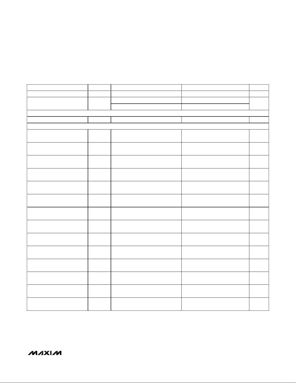
Output Current Capability LRAPD = 0 50 mA
Output Short-Circuit Current LRAPD = 0, AVDD shorted to AGND 100 mA
Maximum AVDD Bypass
Capacitor to AGND
+2.5V (DVDD) LINEAR REGULATOR
DVDD Output Voltage REGEN2 = GNDIO 2.38 2.5 2.62 V
No-Load Quiescent Current
Output Current Capability REGEN2 = GNDIO 50 mA
Output Short-Circuit Current
Maximum DVDD Bypass
Capacitor to DGND
SUPPLY-VOLTAGE SUPERVISORS AND BROWNOUT DETECTION
DVDD Reset Threshold
DVDD Interrupt Threshold
Minimum DVDD Interrupt and
Reset Threshold Difference
AVDD Interrupt Threshold
DVDDIO Interrupt Threshold
Operational Range
Supervisor Hysteresis ±0.7 %
CAN INTERFACE
CAN Baud Rate f
CANCLK Mean Frequency
Error
LRAPD = 0 0.47 µF
REGEN2 = GNDIO, all internal digital
peripherals disabled
REGEN2 = GNDIO, DV
DGND
REGEN2 = GNDIO 0.47 µF
Asserts RESET if V
threshold
Generates an interrupt if V
below this threshold
Generates an interrupt if V
below this threshold
Generates an interrupt if V
falls below this threshold
DV
DD
AV
DD
DV
DDIO
CANCLK
8MHz or 16MHz, 50ppm external
crystal
shorted to
DD
is below this
DVDD
falls
DVDD
falls
AVDD
DVDDIO
= 8MHz 1 Mbps
2.1 2.25 V
2.25 2.38 V
3.0 3.15 V
4.5 4.75 V
1 2.75
1 3.6
1 5.25
15 µA
100 mA
0.14 V
60 ppm
V
CANCLK Total Frequency Error
8MHz or 16MHz, 50ppm external
crystal; measured over a 12ms
interval; mean plus peak cycle jitter
< 0.5 %
Page 6
MAXQ7670
Microcontroller with 10-Bit ADC,
PGA, 64KB Flash, and CAN Interface
6 _______________________________________________________________________________________
ELECTRICAL CHARACTERISTICS (continued)
(V
DVDDIO
= +5.0V, V
AVDD
= +3.3V, V
DVDD
= +2.5V, V
REFADC
= +3.3V, system clock = 16MHz. TA= T
MIN
to T
MAX
, unless otherwise
noted. Typical values are at T
A
= +25°C.) (Note 1)
PARAMETER SYMBOL CONDITIONS MIN TYP MAX UNITS
HIGH-FREQUENCY CRYSTAL OSCILLATOR
Clock Frequency
Stability Excluding crystal drift 25 ppm
Startup Time f
XIN Input Low Voltage Driven with external clock source
XIN Input High Voltage Driven with external clock source
INTERNAL FIXED-FREQUENCY OSCILLATOR
Frequency f
Tolerance TA = +25°C ±0.4 %
Temperature Drift TA = T
Power-Supply Rejection TA = +25°C, DV
RESET (RESET)
RESET Internal Pullup
Resistance
RESET Output Low Voltage RESET asserted, no external load 0.4 V
RESET Output High Voltage RESET deasserted, no external load
RESET Input Low Voltage Driven with external clock source
RESET Input High Voltage Driven with external clock source
DIGITAL INPUTS (P0._, CANRXD, MISO, MOSI, SS, SCLK, TCK, TDI, TMS)
Input Low Voltage 0.8 V
Input High Voltage 2.1 V
Input Hysteresis 500 mV
Input Leakage Current
Input Pullup Resistance 55 kΩ
Input Pulldown Resistance 55 kΩ
Input Capacitance 15 pF
DIGITAL OUTPUTS (P0._, CANTXD, MOSI, SCLK, SS, TDO)
Output Low Voltage I
Output High Voltage I
IFFCLKTA
Using external crystal 8 or 16 16
External input (Note 10) 0.166 16.67
SYSCLK
= T
MIN
MIN
Pulled up to DVDDIO 55 kΩ
V
= GNDIO or V
IN
pullup disabled
= 0.5mA 0.4 V
SINK
SOURCE
cycles 65,535 Cycles
0.7 x
V
DVDD
to T
MAX
to T
MAX
= 0.5mA
= 2.25V to 2.75V ±1.5 %
DD
,
DVDDIO
13.8 15 16.35 MHz
0.9 x
V
DVDDIO
0.7 x
V
DVDDIO
-10 ±0.01 +10 µA
V
DVDDIO
- 0.5
5%
0.3 x
V
DVDD
0.3 x
V
DVDD
MHz
V
V
V
V
V
V
Page 7
MAXQ7670
Microcontroller with 10-Bit ADC,
PGA, 64KB Flash, and CAN Interface
_______________________________________________________________________________________ 7
ELECTRICAL CHARACTERISTICS (continued)
(V
DVDDIO
= +5.0V, V
AVDD
= +3.3V, V
DVDD
= +2.5V, V
REFADC
= +3.3V, system clock = 16MHz. TA= T
MIN
to T
MAX
, unless otherwise
noted. Typical values are at T
A
= +25°C.) (Note 1)
PARAMETER SYMBOL CONDITIONS MIN TYP MAX UNITS
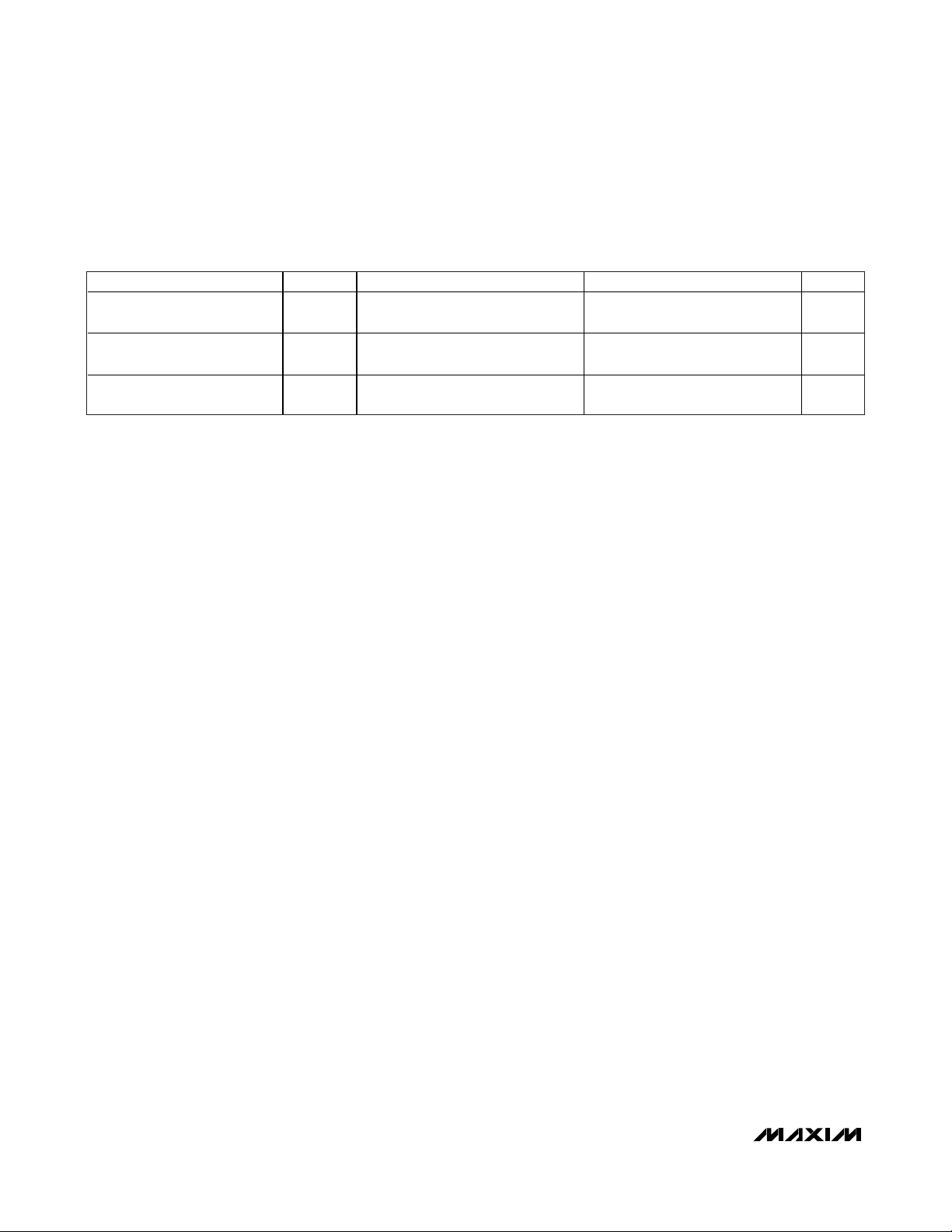
Output Capacitance I/O pins three-state 15 pF
Maximum Output Impedance
PD0._ = 0 880
PD0._ = 1 450
SYSTEM CLOCK
System Clock Frequency f
SYSCLK
From any clock source 0 16.67 MHz
SPI INTERFACE TIMING
SPI Master Operating
Frequency
SPI Slave Mode Operating
Frequency
SCLK Output Pulse-Width
High/Low
SCLK Input Pulse-Width
High/Low
t
SCH
MOSI Output Hold Time
After SCLK Sample Edge
MOSI Output Setup Time to
SCLK Sample Edge
MISO Input Setup Time to
SCLK Sample Edge
MISO Input Hold Time After
SCLK Sample Edge
SCLK Inactive to MOSI
Inactive
MOSI Input Setup Time to
SCLK Sample Edge
MOSI Input Hold Time After
SCLK Sample Edge
MISO Output Valid After
SCLK Shift Edge Transition
MISO Output Disabled After
SS Edge Rise
SS Falling Edge to MISO Active t
f
MCLK
f
SCLK
t
MCH
t
MCL
t
MOH
t
MOS
t
MIS
t
MIH
t
MLH
t
SIS
t
SIH
t
SOV
t
SLH
SOE
0.5 x f
SYSCLK
,
t
SYSCLK
8 MHz
f
/8 MHz
SYSCLK
- 25
, t
SCL
t
SYSCLK
t
SYSCLK
- 25
t
SYSCLK
- 25
30 ns
0ns
t
SYSCLK
- 25
30 ns
t
SYSCLK
+ 25
3 t
SYSCLK
+ 25
2 t
SYSCLK
+ 50
2 t
SYSCLK
+ 2.5
Ω
ns
ns
ns
ns
ns
ns
ns
ns
ns
Page 8
MAXQ7670
Microcontroller with 10-Bit ADC,
PGA, 64KB Flash, and CAN Interface
8 _______________________________________________________________________________________
Note 1: All devices are 100% production tested at TA= +25°C and +125°C. Temperature limits to TA= -40°C are guaranteed by
design.
Note 2: All analog functions disabled and all digital inputs connected to supply or ground.
Note 3: High-speed/8 mode without CAN; V
DVDD
= +2.5V, CPU and 16-bit timer running at 2MHz from an external, 16MHz crystal
oscillator; all other peripherals disabled; all digital I/Os static at V
DVDDIO
or GNDIO; TA= T
MIN
to T
MAX
.
Note 4: High-speed/1 mode with CAN; V
DVDD
= +2.5V, CPU and 16-bit timer running at 16MHz from an external, 16MHz crystal
oscillator; CAN enabled and communicating at 500kbps; all other peripherals disabled, all digital I/Os (except CANTXD
and CANRXD) static at V
DVDDIO
or GNDIO, TA= T
MIN
to T
MAX
.
Note 5: Low speed, PMM1 mode without CAN; V
DVDD
= +2.5V, CPU and one timer running from an external, 16MHz crystal oscilla-
tor in PMM1 mode; all other peripherals disabled; all digital I/Os static at V
DVDDIO
or GNDIO, TA= T
MIN
to T
MAX
.
Note 6: CAN transmitting at 500kbps; 16-bit timer output switching at 500kHz; all active I/Os are loaded with a 20pF capacitor; all
remaining digital I/Os are static at V
DVDDIO
or GNDIO, TA= T
MIN
to T
MAX
.
Note 7: Guaranteed by design and characterization.
Note 8: This is not a static capacitance. It is the capacitance presented to the analog input when the T/H amplifier is in sample mode.
Note 9: The switched capacitor on the REFADC input can disturb the reference voltage. To reduce this disturbance, place a 0.1µF
capacitor from REFADC to AGND as close as possible to REFADC.
Note 10: The digital design is fully static. However, the lower clock limit is set by a clock detect circuit. The MAXQ7670 switches to
the internal RC clock if the external input goes below 166kHz. This clock detect circuit also acts to detect a crystal failure
when a crystal is used.
ELECTRICAL CHARACTERISTICS (continued)
(V
DVDDIO
= +5.0V, V
AVDD
= +3.3V, V
DVDD
= +2.5V, V
REFADC
= +3.3V, system clock = 16MHz. TA= T
MIN
to T
MAX
, unless otherwise
noted. Typical values are at T
A
= +25°C.) (Note 1)
PARAMETER SYMBOL CONDITIONS MIN TYP MAX UNITS
SS Falling Edge to First SCLK
Sample Edge
SCLK Inactive to SS Rising
Edge
Minimum CS Pulse Width t
t
SSE
t
SD
SCW
2 t
SYSCLK
+ 5
t
SYSCLK
+ 10
t
SYSCLK
+ 10
ns
ns
ns
Page 9
MAXQ7670
Microcontroller with 10-Bit ADC,
PGA, 64KB Flash, and CAN Interface
_______________________________________________________________________________________ 9
(CKPOL/CKPHA =
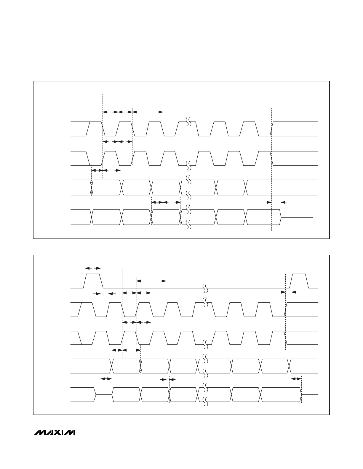
Figure 1. SPI Timing Diagram in Master Mode
Figure 2. SPI Timing Diagram in Slave Mode
SCLK
0/1 OR 1/0 MODE)
SCLK
(CKPOL/CKPHA =
0/0 OR 1/1 MODE)
MISO
MOSI
SAMPLE EDGE
SHIFT EDGE
t
t
t
MCH
MCL
t
t
MCL
MCH
t
MIH
t
MIS
MCLK
t
MOS
t
MOH
t
MLH
HIGH IMPEDANCE
t
SCW
SS
SCLK
(CKPOL/CKPHA =
0/1 OR 1/0 MODE)
SCLK
(CKPOL/CKPHA =
0/0 OR 1/1 MODE)
MOSI
MISO
t
SOE
HIGH
IMPEDANCE
SAMPLE EDGE
SHIFT EDGE
t
t
SCL
SSE
t
SCHtSCL
t
t
SIS
t
SCLK
t
t
SCH
SIH
t
SOV
SD
t
SLH
HIGH
IMPEDANCE
Page 10
MAXQ7670
Microcontroller with 10-Bit ADC,
PGA, 64KB Flash, and CAN Interface
10 ______________________________________________________________________________________
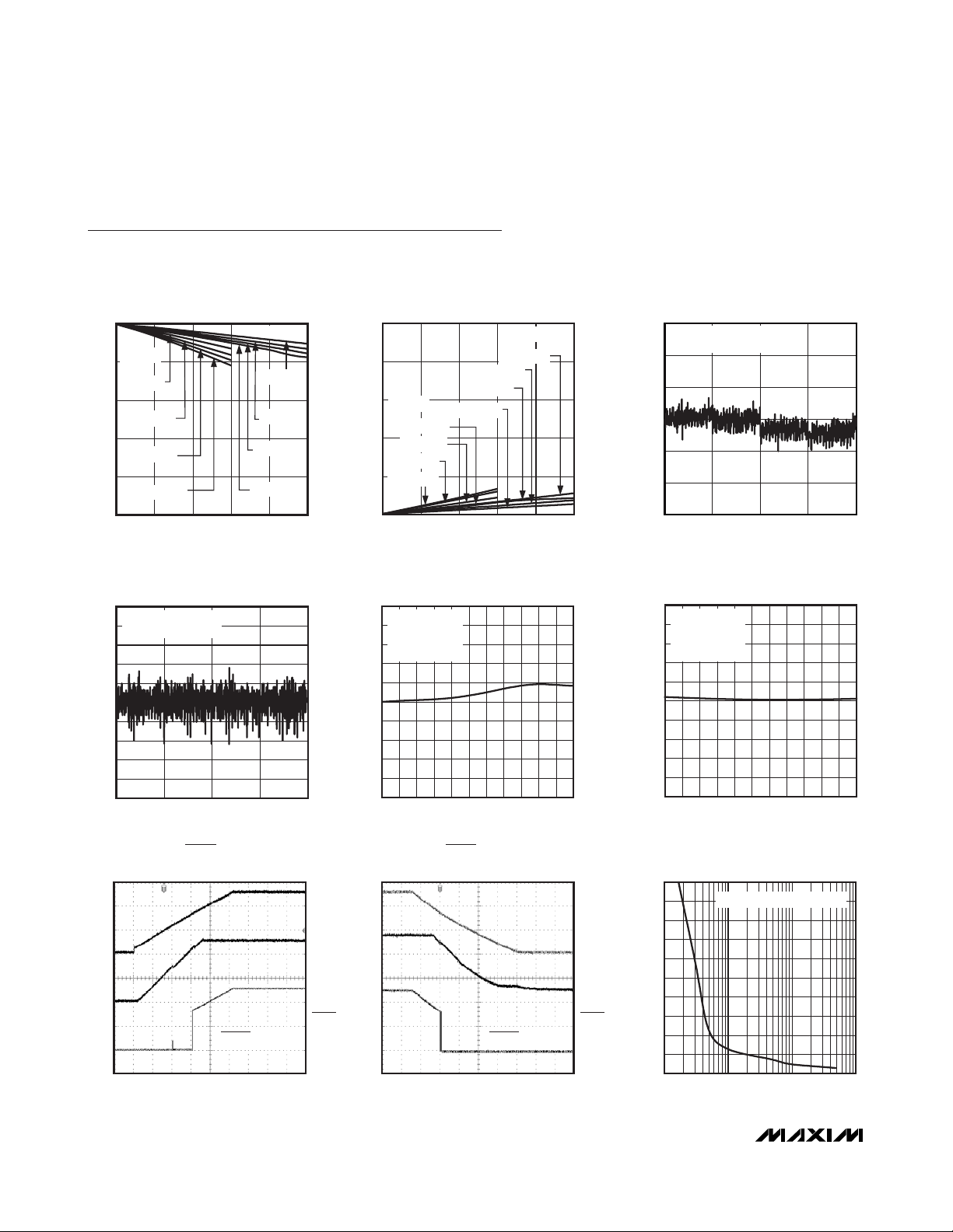
Typical Operating Characteristics
(V
DVDDIO
= 5.0V, V
AVDD
= 3.3V, V
DVDD
= 2.5V, f
SYSCLK
= 16MHz, ADC resolution = 10 bits, V
REFDAC
= 3.3V, TA = +25°C, unless
otherwise noted.)
(V)
OH
V
1.0
0.8
0.6
0.4
0.2
-0.2
ADC DNL (LSB)
-0.4
-0.6
-0.8
-1.0
GPO._ OUTPUT HIGH VOLTAGE
vs. SOURCE CURRENT
5
PS0._ = 0
4
TA = -40°C
3
TA = +25°C
2
TA = +85°C
1
TA = +105°C
0
0 0.5 1.0 1.5 2.0 2.5
IOH (mA)
PS0._ = 1
TA = -40°C
TA = +25°C
TA = +85°C
TA = +105°C
ADC DNL vs. CODE
(REFADC = +3.3V, 150.9ksps,
PGA GAIN = 16V/V)
BIPOLAR MODE
= -100mV to +100mV
V
IN
0
-512 -256 0 256 512
DIGITAL OUTPUT CODE
DVDD, RESET POWER-UP
CHARACTERISTICS
10ms/div
MAXQ7670 toc07
REGEN2 = GNDIO
MAXQ7670 toc01
MAXQ7670 toc04
DVDDIO
2V/div
DVDD
1V/div
RESET
2V/div
GPO._ OUTPUT LOW VOLTAGE
vs. SINK CURRENT
5
4
3
PS0._ = 0
(V)
OL
V
TA = -40°C
2
TA = +25°C
TA = +85°C
1
TA = +105°C
0
0 0.5 1.0 1.5 2.0 2.5
TA = +105°C
TA = +85°C
TA = +25°C
TA = -40°C
IOL (mA)
ADC OFFSET ERROR vs. TEMPERATURE
2.0
BIPOLAR MODE
1.8
PGA GAIN = 16V/V
= 0
V
IN-DIFF
1.6
1.4
1.2
1.0
0.8
OFFSET ERROR (mV)
0.6
0.4
0.2
0
= +1.65V
V
IN-CM
-40 -25 -10 5 20 35 50 65 80 95 110 125
TEMPERATURE (°C)
DVDD, RESET POWER-DOWN
CHARACTERISTICS
REGEN2 = GNDIO
20ms/div
PS0._ = 1
MAXQ7670 toc08
MAXQ7670 toc02
MAXQ7670 toc05
DVDDIO
2V/div
DVDD
1V/div
RESET
2V/div
ADC INL vs. CODE
(REF ADC = +3.3V, 150.9ksps, PGA GAIN = 16V/V)
1.5
BIPOLAR MODE
= -100mV TO +100mV
V
IN
1.0
0.5
0
ADC INL (LSB)
-0.5
-1.0
-1.5
-512 -256 0 256 512
DIGITAL OUTPUT CODE
ADC GAIN ERROR vs. TEMPERATURE
1.0
BIPOLAR MODE
0.8
PGA GAIN = 16V/V
= 200mV
V
IN-DIFF
0.6
0.4
0.2
0
-0.2
GAIN ERROR (%)
-0.4
-0.6
-0.8
-1.0
= +1.65V
V
IN-CM
-40 -25 -10 5 20 35 50 65 80 95 110 125
TEMPERATURE (°C)
MAXIMUM DVDD TRANSIENT DURATION
vs. BOI THRESHOLD OVERDRIVE
200
180
160
140
120
100
80
60
40
MAXIMUM TRANSIENT DURATION (µs)
20
0
1 10 100 1000
BOI ASSERTED ABOVE THIS LINE
DVDD BOI THRESHOLD OVERDRIVE (mV)
MAXQ7670 toc03
MAXQ7670 toc06
MAXQ7670 toc09
Page 11
MAXQ7670
Microcontroller with 10-Bit ADC,
PGA, 64KB Flash, and CAN Interface
______________________________________________________________________________________
11
E
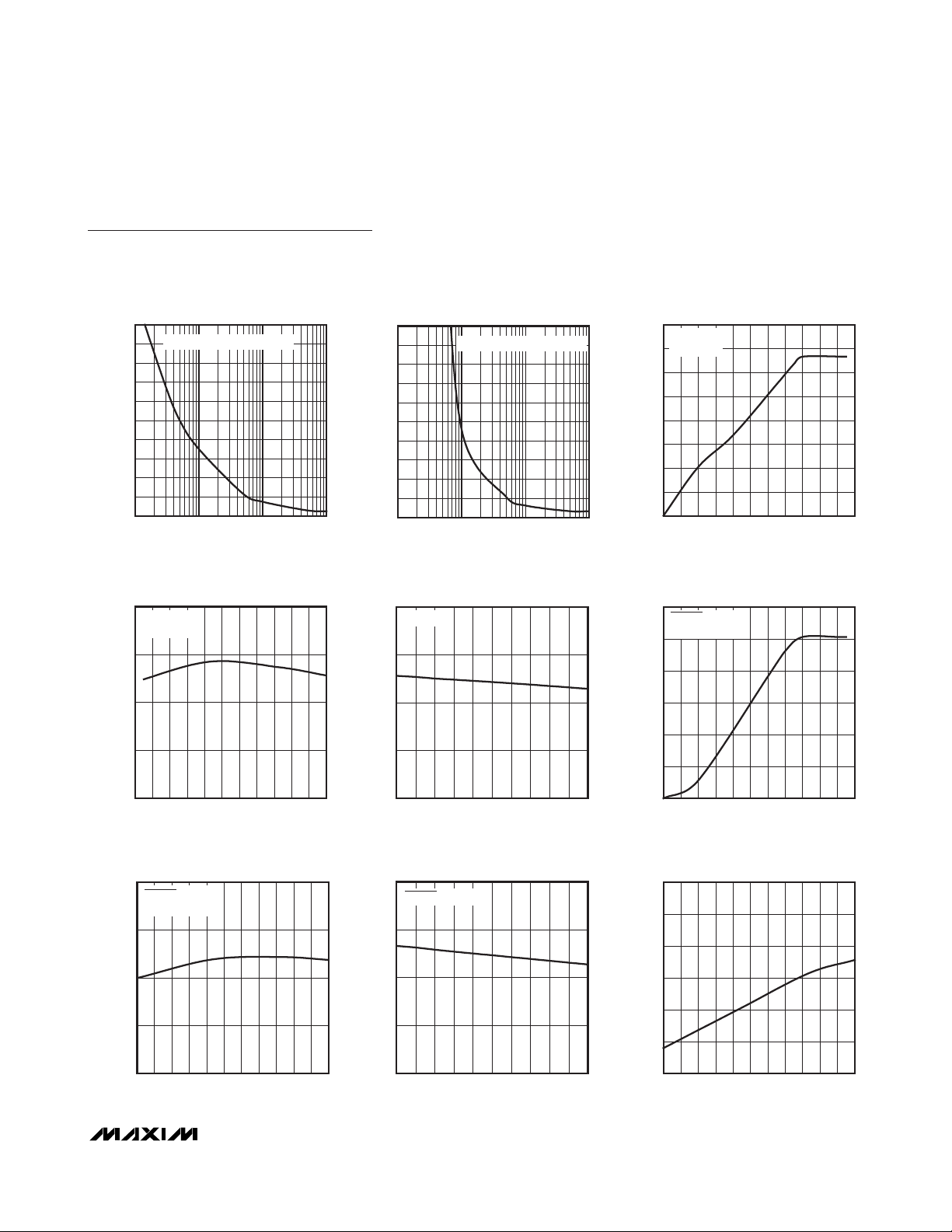
Typical Operating Characteristics (continued)
(V
DVDDIO
= 5.0V, V
AVDD
= 3.3V, V
DVDD
= 2.5V, f
SYSCLK
= 16MHz, ADC resolution = 10 bits, V
REFDAC
= 3.3V, TA = +25°C, unless
otherwise noted.)
MAXIMUM DVDDIO TRANSIENT DURATION
vs. BOI THRESHOLD OVERDRIVE
200
180
160
140
120
100
80
60
40
MAXIMUM TRANSIENT DURATION (µs)
20
BOI ASSERTED ABOVE THIS LINE
0
1 10 100 1000
DVDDIO BOI THRESHOLD OVERDRIVE (mV)
AVDD LINEAR REGULATOR OUTPUT VOLTAGE
vs. TEMPERATURE
3.40
LRAPD = 0
= 10mA
I
OUT
3.35
MAXQ7670 toc10
MAXQ7670 toc13
MAXIMUM AVDD TRANSIENT DURATION
vs. BOI THRESHOLD OVERDRIVE
200
180
160
140
120
100
80
60
40
MAXIMUM TRANSIENT DURATION (µs)
20
0
1 10 100 1000
BOI ASSERTED ABOVE THIS LINE
AVDD BOI THRESHOLD OVERDRIVE (mV)
AVDD LINEAR REGULATOR OUTPUT VOLTAGE
vs. LOAD CURRENT
3.40
LRAPD = 0
3.35
MAXQ7670 toc11
AVDD (V)
MAXQ7670 toc14
AVDD LINEAR REGULATOR OUTPUT VOLTAGE
vs. DVDDIO SUPPLY VOLTAGE
4.0
LRAPD = 0
= 10mA
I
3.5
OUT
3.0
2.5
2.0
1.5
1.0
0.5
0
0 0.5 1.0 1.5 2.0 2.5 3.0 3.5 4.0 4.5 5.0 5.5
DVDDIO (V)
DVDD LINEAR REGULATOR OUTPUT VOLTAGE
vs. DVDDIO SUPPLY VOLTAGE
3.0
REGEN2 = DVDDIO
= 10mA
I
OUT
2.5
2.0
MAXQ7670 toc12
MAXQ7670 toc15
3.30
AVDD (V)
3.25
3.20
-40 -25 -10 5 20 35 50 65 80 95 110 125
TEMPERATURE (°C)
DVDD LINEAR REGULATOR OUTPUT VOLTAG
vs. TEMPERATURE
2.60
REGEN2 = DVDDIO
= 10mA
I
OUT
2.55
2.50
DVDD (V)
2.45
2.40
-40 -25 -10 5 20 35 50 65 80 95 110 125
TEMPERATURE (°C)
MAXQ7670 toc16
3.30
AVDD (V)
3.25
3.20
0 5 10 15 20 25 30 35 40 45 50
LOAD CURRENT (mA)
DVDD LINEAR REGULATOR OUTPUT VOLTAGE
vs. LOAD CURRENT
2.60
REGEN2 = DVDDIO
2.55
2.50
DVDD (V)
2.45
2.40
0 5 10 15 20 25 30 35 40 45 50
LOAD CURRENT (mA)
MAXQ7670 toc17
1.5
DVDD (V)
1.0
0.5
0
0 0.5 1.0 1.5 2.0 2.5 3.0 3.5 4.0 4.5 5.0 5.5
DVDDIO (V)
RC OSCILLATOR OUTPUT FREQUENCY
vs. TEMPERATURE
17.0
16.5
16.0
15.5
15.0
FREQUENCY (MHz)
14.5
14.0
-40 -25 -10 5 20 35 50 65 80 95 110 125
TEMPERATURE (°C)
MAXQ7670 toc18
Page 12
MAXQ7670
Microcontroller with 10-Bit ADC,
PGA, 64KB Flash, and CAN Interface
12 ______________________________________________________________________________________
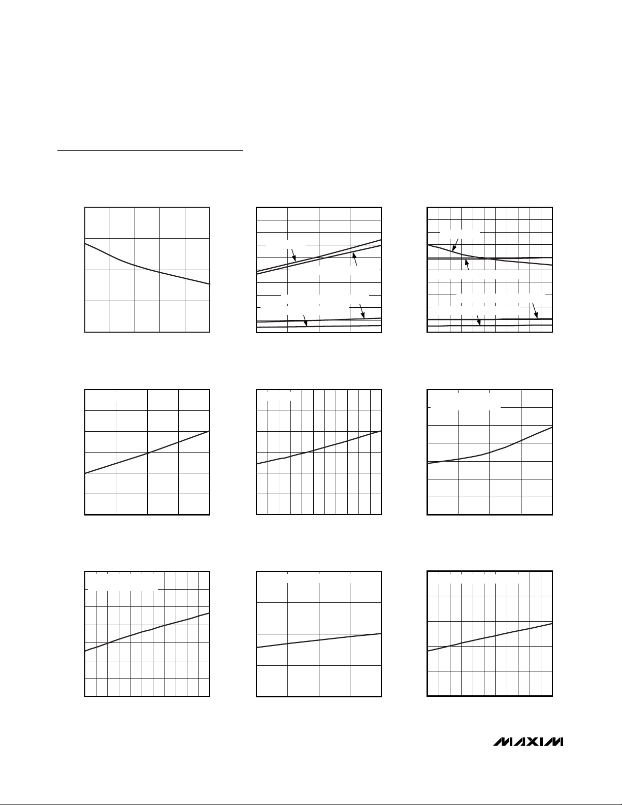
Typical Operating Characteristics (continued)
(V
DVDDIO
= 5.0V, V
AVDD
= 3.3V, V
DVDD
= 2.5V, f
SYSCLK
= 16MHz, ADC resolution = 10 bits, V
REFDAC
= 3.3V, TA = +25°C, unless
otherwise noted.)
RC OSCILLATOR OUTPUT FREQUENCY
vs. DVDD
16.0
15.5
15.0
FREQUENCY (MHz)
14.5
14.0
2.25 2.35 2.45 2.55 2.65 2.75
DVDD (V)
20
18
16
MAXQ7670 toc19
14
12
10
8
6
DVDD SUPPLY CURRENT (mA)
4
2
0
DVDD SUPPLY CURRENT
vs. DVDD SUPPLY VOLTAGE
FLASH ERASE
EC CHARACTERISTICS
NOTE 4 IN
EC CHARACTERISTICS
NOTE 3 IN
EC CHARACTERISTICS
NOTE 5 IN
2.250 2.750
DVDD SUPPLY VOLTAGE (V)
2.6252.5002.375
MAXQ7670 toc020
DVDD SUPPLY CURRENT
vs. TEMPERATURE
20
18
16
FLASH ERASE
14
12
10
8
6
DVDD SUPPLY CURRENT (mA)
4
2
0
-40 125
NOTE 4 IN
NOTE 5 IN
EC CHARACTERISTICS
EC CHARACTERISTICS
NOTE 3 IN
EC CHARACTERISTICS
TEMPERATURE (°C)
MAXQ7670 toc21
1109565 80-10 5 20 35 50-25
DVDD SUPPLY CURRENT
vs. DVDD SUPPLY VOLTAGE
26.5
STOP MODE
26.0
25.5
25.0
24.5
DVDD SUPPLY CURRENT (µA)
24.0
23.5
2.250 2.750
DVDD SUPPLY VOLTAGE (V)
2.6252.5002.375
AVDD SUPPLY CURRENT
vs. TEMPERATURE
140
SHUTDOWN (NOTE 2)
EC CHARACTERISTICS
IN
120
100
80
60
40
AVDD SUPPLY CURRENT (nA)
20
28
STOP MODE
27
MAXQ7670 toc22
26
25
24
DVDD SUPPLY CURRENT (µA)
23
22
-40 125
6.0
ALL ANALOG FUNCTIONS ENABLED
MAXQ7670 toc25
5.9
5.8
5.7
AVDD SUPPLY CURRENT (mA)
DVDD SUPPLY CURRENT
vs. TEMPERATURE
TEMPERATURE (°C)
AVDD SUPPLY CURRENT
vs. AVDD SUPPLY VOLTAGE
AVDD SUPPLY CURRENT
vs. AVDD SUPPLY VOLTAGE
140
SHUTDOWN (NOTE 2)
EC CHARACTERISTICS
IN
120
MAXQ7670 toc23
100
80
60
40
AVDD SUPPLY CURRENT (nA)
20
1109580655035205-10-25
0
3.00 3.60
AVDD SUPPLY VOLTAGE (V)
3.453.303.15
MAXQ7670 toc24
AVDD SUPPLY CURRENT
vs. TEMPERATURE
6.2
ALL ANALOG FUNCTIONS ENABLED
6.0
MAXQ7670 toc26
5.8
5.6
AVDD SUPPLY CURRENT (mA)
5.4
MAXQ7670 toc27
0
-40 125
TEMPERATURE (°C)
1109565 80-10 5 20 35 50-25
5.6
3.00 3.60
AVDD SUPPLY VOLTAGE (V)
3.453.303.15
5.2
-40 125
TEMPERATURE (°C)
1109580655035205-10-25
Page 13

MAXQ7670
Microcontroller with 10-Bit ADC,
PGA, 64KB Flash, and CAN Interface
______________________________________________________________________________________
13
Typical Operating Characteristics (continued)
(V
DVDDIO
= 5.0V, V
AVDD
= 3.3V, V
DVDD
= 2.5V, f
SYSCLK
= 16MHz, ADC resolution = 10 bits, V
REFDAC
= 3.3V, TA = +25°C, unless
otherwise noted.)
DVDDIO INCREMENTAL SUPPLY CURRENT
vs. DVDDIO SUPPLY VOLTAGE
MAXQ7670 toc33
DVDDIO SUPPLY VOLTAGE (V)
DVDDIO SUPPLY CURRENT (µA)
5.1255.0004.875
1
2
3
4
5
0
4.750 5.250
BOI ENABLED
DVDDIO INCREMENTAL SUPPLY CURRENT
vs. TEMPERATURE
MAXQ7670 toc34
TEMPERATURE (°C)
DVDDIO SUPPLY CURRENT (µA)
5-10-25 503520 110958065
1
2
3
4
5
0
-40 125
BOI ENABLED
ADC SAMPLING ERROR
vs. INPUT SOURCE IMPEDANCE
SOURCE IMPEDANCE (Ω)
SAMPLING ERROR (LSB)
MAXQ7670 toc35
-5
-4
-3
-2
-1
0
1
1 10 100 1000 10,000 100,000
PGA GAIN = 16V/V
f
S
= 150.9ksps
AVDD SUPPLY CURRENT
vs. ADC SAMPLING RATE
5.7
PGA GAIN = 16V/V
5.6
5.5
AVDD SUPPLY CURRENT (mA)
5.4
1 1000
10 100
ADC SAMPLING RATE (ksps)
DVDDIO STATIC SUPPLY CURRENT
vs. DVDDIO SUPPLY VOLTAGE
160
140
120
MAXQ7670 toc28
MAXQ7670 toc31
DVDDIO DYNAMIC SUPPLY CURRENT
vs. DVDDIO SUPPLY VOLTAGE
260
240
220
200
180
160
140
DVDDIO SUPPLY CURRENT (µA)
120
100
2.250 2.750
EC CHARACTERISTICS
NOTE 6 IN
DVDDIO SUPPLY VOLTAGE (V)
2.6252.5002.375
DVDDIO STATIC SUPPLY CURRENT
vs. TEMPERATURE
160
140
120
MAXQ7670 toc29
DVDDIO SUPPLY CURRENT (µA)
MAXQ7670 toc32
250
240
230
220
210
200
DVDDIO DYNAMIC SUPPLY CURRENT
vs. TEMPERATURE
EC CHARACTERISTICS
NOTE 6 IN
-40 125
TEMPERATURE (°C)
1109580655035205-10-25
MAXQ7670 toc30
100
80
DVDDIO SUPPLY CURRENT (µA)
60
40
4.750 5.250
DVDDIO SUPPLY VOLTAGE (V)
100
80
DVDDIO SUPPLY CURRENT (µA)
60
40
5.1255.004.875
-40 125
TEMPERATURE (°C)
1109580655035205-10-25
SNR
0
-20
-40
-60
-80
MAGNITUDE (dB)
-100
-120
-140
0 5 10 15 20 25 30 35
FREQUENCY (kHz)
fIN = 10kHz
= 62.5ksps
f
S
MAXQ7670 toc36
Page 14

MAXQ7670
Microcontroller with 10-Bit ADC,
PGA, 64KB Flash, and CAN Interface
14 ______________________________________________________________________________________
Pin Description
PIN NAME FUNCTION
1 AIN7
2 AIN6
3 AIN5
4 AIN4
5 REFADC ADC External Reference Input. Connect an external reference between 1V and V
6 AGND Analog Ground
7 AIN3
8 AIN2
9 AIN1
10 AIN0
11 I.C. Internally Connected. Connect to GNDIO for proper operation.
12 P0.0 Port 0 Bit 0. P0.0 is a general-purpose digital I/O with interrupt/wake-up capability.
13 P0.1 Port 0 Bit 1. P0.1 is a general-purpose digital I/O with interrupt/wake-up capability.
14 P0.2 Port 0 Bit 2. P0.2 is a general-purpose digital I/O with interrupt/wake-up capability.
15, 22, 38 GNDIO Digital I/O Ground and Regulator Ground
16 CANRXD CAN Bus Receiver Input. CAN receiver input.
17 CANTXD CAN Bus Transmitter Output. CAN transmitter output.
18 SS
Analog Input Channel 7. AIN7 is multiplexed to the PGA or ADC as single-ended analog input 7 or as a
differential input with AIN6. As a differential input, the polarity of AIN7 is negative.
Analog Input Channel 6. AIN6 is multiplexed to the PGA or ADC as a single-ended analog input 6 or as a
differential input with AIN7. As a differential input, the polarity of AIN6 is positive.
Analog Input Channel 5. AIN5 is multiplexed to the PGA or ADC as single-ended analog input 5 or as a
differential input with AIN4. As a differential input, the polarity of AIN5 is negative.
Analog Input Channel 4. AIN4 is multiplexed to the PGA or ADC as single-ended analog input 4 or as a
differential input with AIN5. As a differential input, the polarity of AIN4 is positive.
Analog Input Channel 3. AIN3 is multiplexed to the PGA or ADC as single-ended analog input 3 or as a
differential input with AIN2. As a differential input, the polarity of AIN3 is negative.
Analog Input Channel 2. AIN2 is multiplexed to the PGA or ADC as single-ended analog input 2 or as a
differential input with AIN3. As a differential input, the polarity of AIN2 is positive.
Analog Input Channel 1. AIN1 is multiplexed to the PGA or ADC as single-ended analog input 1 or as a
differential input with AIN0. As a differential input, the polarity of AIN1 is negative.
Analog Input Channel 0. AIN0 is multiplexed to the PGA or ADC as single-ended analog input 0 or as a
differential input with AIN1. As a differential input, the polarity of AIN0 is positive.
Active-Low, SPI Port Slave Select Input. In SPI slave mode, this is the slave select input. In SPI master
mode, this is an input and connection is optional (connect if mode fault enable is required, refer to the
MAXQ7670 User’s Guide for a description of the SPICN register). In master mode, use an available GPIO
as a slave selector and pull SS high to DVDDIO through a pullup resistor.
.
AVDD
Port 0 Bit 6/Timer 0 I/O. P0.6 is a general-purpose digital I/O with interrupt/wake-up input capability. T0 is a
19 P0.6/T0
20 P0.7/T0B
21, 39 DVDDIO
primary timer/PWM input or output. The alternative function, T0, is selected using the T2CNA0 register.
When this function is selected, it overrides the GPIO functionality.
Port 0 Bit 7/Timer 0 Output. P0.7 is a general-purpose digital I/O with interrupt/wake-up input capability.
T0B is a secondary timer/PWM output. The alternative function, T0B, is selected using the T2CNB0 register.
When this function is selected, it overrides the GPIO functionality.
Digital I/O Supply Voltage and Regulator Supply Input. DVDDIO supplies all digital I/O except for XIN and
XOUT, and supplies power to the two internal linear regulators, AVDD and DVDD. Bypass DVDDIO to
GNDIO with a 0.1µF capacitor as close as possible to the device.
Page 15

MAXQ7670
Microcontroller with 10-Bit ADC,
PGA, 64KB Flash, and CAN Interface
______________________________________________________________________________________ 15
Pin Description (continued)
PIN NAME FUNCTION
23 SCLK
24 MOSI
25 MISO
26 REGEN2
27 TDO JTAG Serial Test Data Output. TDO is the JTAG serial test, data output.
28 TMS JTAG Test Mode Select. TMS is the JTAG test mode, select input.
29 TDI JTAG Serial Test Data Input. TDI is the JTAG serial test, data input.
30 TCK JTAG Serial Test Clock Input. TCK is the JTAG serial test, clock input.
31
32 P0.5 Port 0 Bit 5. P0.5 is a general-purpose digital I/O with interrupt/wake-up capability.
33 RESET
34 DGND Digital Ground
35 XOUT
P0.4/
ADCCNV
SPI Serial Clock. SCLK is the SPI interface serial clock I/O. In SPI master mode, SCLK is an output. While in
SPI slave mode, SCLK is an input.
SPI Serial Data I/O. MOSI is the SPI interface serial data output in master mode or serial data input in slave
mode.
SPI Serial Data I/O. MISO is the SPI interface serial data input in master mode or serial data output in slave
mode.
Active-Low +2.5V Linear Regulator Enable Input. Connect REGEN2 to GNDIO to enable the +2.5V linear
regulator. Connect to DVDDIO to disable the +2.5V linear regulator.
Port 0 Bit 4/ADC Start Conversion Control. P0.4 is a general-purpose digital I/O with interrupt/wake-up
capability. ADCCNV is a firmware-configurable, rising or falling edge, start/convert signal used to trigger
ADC conversions. The alternative function, ADCCNV, is selected using the register bits ACNT[2:0]. When
using ADCCNV as a trigger for ADC conversion, set P0.4/ADCCNV as an input using the PD0 register. This
action prevents any unintentional interference in the SARADC operation.
Reset Input/Output. Active-low input/output with internal 55kΩ pullup to DVDDIO. Drive low to reset the
MAXQ7670. The MAXQ20 µC core holds RESET low during POR and during DVDD brownout conditions.
High-Frequency Crystal Output. Connect an external crystal to XIN and XOUT for normal operation, or leave
unconnected if XIN is driven with an external clock source. Leave unconnected if an external clock source
is not used.
36 XIN
37 DVDD
40 AVDD
— EP Exposed Pad. Connect EP to the ground plane.
H i g h- Fr eq uency C r ystal Inp ut. C onnect an exter nal cr ystal or r esonator to X IN and X OU T for nor m al op er ati on,
or d r i ve X IN w i th an exter nal cl ock sour ce. Leave unconnected i f an exter nal cl ock sour ce i s not used .
D i g i tal S up p l y V ol tag e. D V D D sup p l i es i nter nal d i g i tal cor e and fl ash m em or y. D V D D i s d i r ectl y connected to
the outp ut of the i nter nal + 2.5V l i near r eg ul ator . D i sab l e the i nter nal r eg ul ator ( thr oug h REG EN 2) to connect an
exter nal sup p l y. Byp ass D V D D to D GN D w i th a 0.1µF cap aci tor as cl ose as p ossi b
Analog Supply Voltage. AVDD supplies PGA and ADC. AVDD is directly connected to the output of the
internal +3.3V linear regulator. Disable the internal regulator (via software) to connect an external supply.
Bypass AVDD to AGND with a 0.1µF capacitor as close as possible to the device.
l e to the d evi ce.
Page 16

MAXQ7670
Microcontroller with 10-Bit ADC,
PGA, 64KB Flash, and CAN Interface
16 ______________________________________________________________________________________
Block Diagram
DVDDIO
AIN0
AIN1
AIN2
AIN3
AIN4
AIN5
AIN6
AGND
REGEN2
RESET
DVDD
TCK
TMS
TDO
XOUT
GNDIO
DGND
AIN7
DVDDIO
DVDDIO
+2.5V
LINEAR
REGAULATOR
GNDIO
DGND
DVDDIO
TDI
XIN
GNDIO
DGND
DVDD
HF
XTAL
OSC.
DGND
BUFFERS
GNDIO
INT
FIXED
FREQ
OSC.
IFE
I/O
AIN1
AIN3
AIN5
AIN7
AIN9
HFFINT
XHFRY
HFE
DVDD
POWER-ON
RESET
MONITOR
VDPE
JTAG INTERFACE
M
U
X
10:1
MUX
6:1
MUX
MAXQ7670
DVDDIO
PORT 0
I/O REGISTERS
HFCLK
IFFCLK
SYSCLK
PGAE
DVDD
DGND
GAIN = 1x, 16x
ADCMX[3:0]
IFFCLK
EWT
UTILITY ROM
64KB (32K x 16)
PROGRAM/DATA
FLASH
2KB (1K x 16)
DATA RAM
CAN CLOCK
PRESCALER
ADC CLOCK
PRESCALER
HF CLOCK
PRESCALER
TIMER CLOCK
PRESCALER
PGA
4K x 16
HFFINT
EIFO
WATCHDOG
TIMER
WTR
SPI
ADCREF
ADCE
WDI
CANCLK
ADCCLK
2:1
T0CLK
M
10-BIT ADC
U
X
ADCCNV
ADCRY
SOFTWARE-
INTERRUPT
CONTROLLER
DV
DD
16-BIT
MAXQ20 CORE
RISC CPU
DGND
ADCBY
SYSCLK
ADCCLK
CANSTI
CANERI
T0I
CANSTI
CANERI
T0CLK
PD0
PO0
PI0
EIF0
DVDDIO
T0I
SPI
VABI
VIOBI
CANCLK
LRAPD
+3.3V
LINEAR
REGAULATOR
GNDIO
AVDD BROWNOUT
MONITOR
DVDDIO BROWNOUT
MONITOR
16-BIT TIMER0
PORT 0
I/O REGISTERS
SERIAL PERIPHERAL
INTERFACE (SPI)
CAN 2.0B
INTERFACE
VABE
VIBE
I/O
BUFFERS
DVDDIO
I/O
BUFFERS
GNDIO
AVDD
AGND
DVDDIO
GNDIO
GNDIO
REFADC
AVDD
P0.7/T0B
P0.6/T0
P0.5
P0.4/ADCCNV
P0.2
P0.1
P0.0
SS
SCLK
MOSI
MISO
CANTXD
CANRXD
Page 17

MAXQ7670
Microcontroller with 10-Bit ADC,
PGA, 64KB Flash, and CAN Interface
______________________________________________________________________________________ 17
Detailed Description
The MAXQ7670 incorporates a 16-bit RISC arithmetic
logic unit (ALU) with a Harvard memory architecture
that addresses 64KB (32K x 16) of flash and 2048
bytes (1024 x 16) of RAM memory. This core combined
with digital and analog peripherals provide versatile
data-acquisition functions. The peripherals include up to
seven digital I/Os, a 4-wire SPI interface, a CAN 2.0B
bus, a JTAG interface, a timer, an integrated RC oscillator, two linear regulators, a watchdog timer, three
power-supply supervisors, a 10-bit 250ksps SAR ADC
with programmable-gain amplifier (PGA) and eight single-ended or four differential multiplexed inputs. The
power-efficient MAXQ20 µC core consumes less than
1mA/MIPS. Refer to the
MAXQ7670 User’s Guide
for
more detailed information on configuring and programming the MAXQ7670.
Analog Input Peripheral
The integrated 10-bit ADC employs an ultra-low-power
SAR-based conversion method and operates up to
250ksps with PGA = 1V/V (150.9ksps with PGA =
16V/V). The integrated 8-channel multiplexer (mux) and
PGA allow the ADC to measure eight single-ended (relative to AGND) or four fully differential analog inputs
with software-selectable input ranges through the PGA.
See Figures 3 and 4.
Figure 3. Simplified Analog Input Diagram (Eight Single-Ended Inputs)
MAXQ7670
P0.4/ADCCNV
AIN0
AIN1
AIN2
AIN3
AIN4
AIN5
AIN6
AIN7
8:1
MUX
1V/V OR
16V/V
TIMER 0
ADCBY
ACTL
120
ADCDUL
ADCBIP
ADCRDY
DATA
BUS
PGA
PGG
CONVERSION
CONTROL
10-BIT ADC
250ksps
10
AGND
ADCMX
1 032
REFADC
ADCE
ADC
CLOCK
DIV
1 0
ADCCD
ADCASD
ADCCLK
SOURCE
Page 18

MAXQ7670
Microcontroller with 10-Bit ADC,
PGA, 64KB Flash, and CAN Interface
18 ______________________________________________________________________________________
Figure 4. Simplified Analog Input Diagram (Four Fully Differential Inputs)
P0.4/ADCCNV
AIN0
AIN2
AIN4
AIN6
AIN1
AIN3
AIN5
AIN7
REFADC
4:1
MUX
4:1
MUX
ADCMX
MAXQ7670
1 032
PGG
PGA
1V/V OR
16V/V
TIMER 0
CONVERSION
CONTROL
10-BIT ADC
250ksps
ADCE
ADC
CLOCK
DIV
1 0
ADCCD
ADCBY
ADCRDY
10
ACTL
120
ADCDUL
ADCBIP
DATA
BUS
ADCASD
ADCCLK
SOURCE
Page 19

MAXQ7670
Microcontroller with 10-Bit ADC,
PGA, 64KB Flash, and CAN Interface
______________________________________________________________________________________ 19
The MAXQ7670 ADC uses a fully differential SAR conversion technique and an integrated T/H (track and
hold) block to convert voltage signals into a 10-bit digital result. Both single-ended and differential configurations are implemented using an analog input channel
multiplexer that supports 8 single-ended or 4 differential channels.
In single-ended mode, the mux selects from either of
the ground-referenced analog inputs AIN0–AIN7. In differential input configuration, analog inputs are selected
from the following pairs: AIN0/AIN1, AIN2/AIN3,
AIN4/AIN5, and AIN6/AIN7. Table 1 shows the singleended and differential input configurations possible for
the ADC mux.
Analog Input Track and Hold
A SAR conversion in the MAXQ7670 has different T/H
cycles depending on whether a gain of 1 (bypass) or a
gain of 16 (PGA enabled) is selected.
Gain = 1V/V
In gain = 1V/V, the conversion has a two-stage T/H
cycle. In track mode, a positive input capacitor connects to the signal channel. A negative input capacitor
connects to the reference channel. After the T/H enters
hold mode, the difference between the signal and the
reference channel is converted to a 10-bit value. This
two-stage cycle takes 16 SARCLKs to complete.
Gain = 16V/V
In gain = 16V/V, the conversion has a three-stage T/H
cycle: amplification, ADC track, and ADC hold. First,
the PGA tracks the selected input and reference signals. The PGA amplifies the difference between the two
signals and holds the result for the next stage, ADC
track. The ADC tracks and converts the PGA result into
a 10-bit value. The SAR operation itself does not
change irrespective of the chosen gain. This threestage cycle takes 26.5 SARCLKs to complete. Figure 5
shows the conversion timing differences between gain
= 1V/V and gain = 16V/V.
Table 1. ADC Mux Input Configurations
SAR CHANNEL
SELECT
(REGISTER
ACNT[14:11])
0000 AIN0 AGND Single-ended measurement on AIN0
0001 AIN1 AGND Single-ended measurement on AIN1
0010 AIN2 AGND Single-ended measurement on AIN2
0011 AIN3 AGND Single-ended measurement on AIN3
0100 AIN4 AGND Single-ended measurement on AIN4
0101 AIN5 AGND Single-ended measurement on AIN5
0110 AIN6 AGND Single-ended measurement on AIN6
0111 AIN7 AGND Single-ended measurement on AIN7
1000 — — Reserved
1001 — — Reserved
1010 AIN0 AIN1 AIN0/AIN1
1011 AIN2 AIN3 AIN2/AIN3
1100 AIN4 AIN5 AIN4/AIN5
1101 AIN6 AIN7 AIN6/AIN7
1110 — — Reserved
1111 — — VCIM differential zero offset trim
SIGNAL CHANNEL
INTO ADC
REFERENCE
CHANNEL INTO
ADC
MEASUREMENT TYPE
Page 20

MAXQ7670
Microcontroller with 10-Bit ADC,
PGA, 64KB Flash, and CAN Interface
20 ______________________________________________________________________________________
Input Impedance
The input-capacitance charging rate determines the
time required for the T/H to acquire an input signal. The
required acquisition time lengthens with the increase of
the input signals source resistance. Any source below
5kΩ does not significantly affect the ADC’s performance. A high-impedance source can be accommodated by placing a 1µF capacitor between the input
channel and AGND. The combination of analog-input
source impedance and the capacitance at the analog
input creates an RC filter that limits the analog-input
bandwidth.
Controlling ADC Conversions
Use the following methods to control the ADC conversion timing:
1) Software register bit control
2) Continuous conversion
3) Internal timer (T0)
4) External input through ADCCNV
Refer to the
MAXQ7670 User’s Guide
for more detailed
information on the ADC and mux.
POR and Brownout
The MAXQ7670 operates from a single, external +5V
supply connected to the DVDDIO. DVDDIO is the supply rail for the digital I/O and the supply input for both
integrated linear regulators. The +3.3V linear regulator
powers AVDD, while the +2.5V linear regulator powers
DVDD. Alternatively, connect REGEN2 to DVDDIO and
apply external power supplies to AVDD and DVDD.
Power supplies DVDDIO, DVDD, and AVDD each
include a brownout monitor that alerts the µC through
an interrupt when the corresponding supply voltages
drop below a defined threshold. This condition is generally referred to as brownout interrupt (BOI). Enable
BOI by setting the VABE, VDBE, and VIBE bits in the
APE register. By continually checking for low supply
voltages, appropriate action can be taken for brownout
conditions.
Startup Using Internal Regulators
Once the +5V DVDDIO supply reaches approximately
1.25V, the +2.5V linear regulator turns on and DVDD
begins ramping. Between the DVDD levels of 1V and
the reset threshold, the DVDD monitor holds RESET
low. DVDD releases RESET after reaching the reset
threshold. The MAXQ7670 jumps to the reset vector
location (8000h in the utility ROM). During this time,
DVDD finishes ramping to its nominal voltage of +2.5V.
During this POR time, the software-enabled +3.3V linear regulator remains off. Turn on the +3.3V linear regulator after the MAXQ7670 has completed its bootup
routines and is running application code. To turn on the
+3.3V regulator, set the LRAPD bit in the APE register
to 0. The AVDD supply begins ramping to its nominal
voltage of +3.3V.
Brownout Detectors
The MAXQ7670 features brownout monitors for the +5V
DVDDIO, +3.3V AVDD, and +2.5V DVDD power supplies. When enabled, these monitors generate interrupts
when DVDDIO, AVDD, or DVDD fall below their respective brownout thresholds. Monitoring the supply rails
alerts the µC to brownout conditions so appropriate
action can be taken. Under normal conditions the DVDDIO
brownout monitor signals a falling +5V supply before
the DVDD or AVDD brownout monitors indicate that the
+2.5V or +3.3V are falling. The exceptions to this condition are:
• If either DVDD or AVDD are externally powered and
the source of power is removed
• If there is some type of device failure that pulls the reg-
ulator outputs low without affecting the +5V DVDDIO
supply
Figure 5. Conversion Timing Differences Between Gain = 1V/V and Gain = 16V/V
3 SCLK
SAR CYCLE
PGA = 1V/V
SAR CYCLE
PGA = 16V/V
SAR TRACK HOLD AND SAR CONVERT
7.5 SCLK 6 SCLK 13 SCLK
PGA TRACK PGA HOLD, SAR TRACK HOLD AND SAR CONVERT
13 SCLK
Page 21

MAXQ7670
Microcontroller with 10-Bit ADC,
PGA, 64KB Flash, and CAN Interface
______________________________________________________________________________________ 21
The DVDD reset supervisor resets the MAXQ7670 when
the +2.5V DVDD falls below the reset threshold. The
processor remains in reset until DVDD returns above
the reset threshold. The µC does not execute commands in reset mode. See Figure 6 for the µC response
to DVDD brownout and reset.
Refer to the
MAXQ7670 User’s Guide
for detailed programming information, and a more thorough description of POR and brownout behavior.
Internal 3.3V Linear Regulator
The integrated 3.3V 50mA linear regulator or an external 3.3V supply powers AVDD. The integrated 3.3V regulator is inactive upon power-up. Enable the integrated
regulator with software programming after power-up.
When using an external supply, connect a regulated
3.3V supply to AVDD after applying DVDDIO.
Internal 2.5V Linear Regulator
The integrated 2.5V 50mA linear regulator or an external 2.5V supply applied at DVDD powers DVDD.
Connect REGEN2 to GNDIO to enable the integrated
regulator. Connect REGEN2 to DVDDIO to use an
external supply. When using an external supply, connect a regulated 2.5V supply to DVDD after applying
DVDDIO.
DVDDIO Current Requirements
Both internal linear regulators are capable of supplying
up to 50mA each. When using the regulators to power
AVDD and DVDD and to provide power to external
devices, make sure DVDDIO’s power input can source
a current greater than the sum of the MAXQ7670 supply current and the load currents of the two regulators.
µ
Figure 6. DVDD Brownout and Reset Behavior
NOMINAL
DVDD (+2.5V)
+2.38V
+2.25V
BROWNOUT
INTERRUPT
(BOI)
DGND
DVLVL FLAG
(ASR[14])
DVBI FLAG
(ASR[4])
BROWNOUT
RESET
(BOR)
INTERNAL RESET
RESET OUTPUT
BOR STATE
FLAG ARBITRARILY
CLEARED BY
C
DVDD BROWNOUT
INTERRUPT
THRESHOLD RANGE
VDBE BIT SET BY µC
Page 22

MAXQ7670
Microcontroller with 10-Bit ADC,
PGA, 64KB Flash, and CAN Interface
22 ______________________________________________________________________________________
System Clock Generator
The MAXQ7670 oscillator module provides the master
clock generator that supplies the system clock for the
µC core and all of the peripheral modules. The high-frequency oscillator operates with an 8MHz or 16MHz
crystal. Alternatively, use the integrated RC oscillator in
applications that do not require precise timing. The
MAXQ7670 executes most instructions in a single
SYSCLK period. The oscillator module contains all of
the primary clock generation circuitry. Figure 7 shows a
block diagram of the system clock module.
The MAXQ7670 contains the following features for generating its master clock signal timing source:
• Internal, fast-starting, 15MHz RC oscillator eliminates
external crystal
• Internal high-frequency oscillator that can drive an
external 8MHz or 16MHz crystal
• External high-frequency 0.166MHz to 16MHz clock input
• Power-up timer
• Power-saving management modes
• Fail-safe modes
Watchdog Timer
The primary function of the watchdog timer is to supervise software execution, watching for stalled or stuck
software. The watchdog timer performs a controlled
system restart when the µC fails to write to the watchdog timer register before a selectable timeout interval
expires. A watchdog timer typically has four objectives:
1) To detect if a system is operating normally
2) To detect an infinite loop in any of the tasks
3) To detect an arbitration deadlock involving two or
more tasks
4) To detect if some lower priority tasks are not getting
to run because of higher priority tasks
As illustrated in Figure 8, the internal RC oscillator
(CLK_RC) drives the watchdog timer through a series
of dividers. The programmable divider output determines the timeout interval. When enabled, the interrupt
flag WDIF sets. A system reset occurs after a time
delay (based on the divider ratio) unless an interrupt
service routine clears the watchdog interrupt.
The watchdog timer functions as the source of both the
watchdog interrupt and the watchdog reset. The interrupt timeout has a default divide ratio of 2
12
of the
CLK_RC, with the watchdog reset set to timeout 2
9
clock cycles later. With the nominal RC oscillator value
of 15MHz, an interrupt timeout occurs every 0.273ms,
followed by a watchdog reset 34µs later. The watchdog
timer resets to the default divide ratio following any
reset event. Use the WD0 and WD1 bits in the WDCN
register to increase the watchdog interrupt period.
Changing the WD[1:0] bits before a watchdog interrupt
timeout occurs (i.e. before the watchdog reset counter
begins) resets the watchdog timer count. The watchdog reset timeout occurs 512 RC oscillator cycles after
the watchdog interrupt timeout. For more information on
the MAXQ7670 watchdog timer, refer to the
MAXQ7670
User’s Guide.
Figure 7. High-Frequency and RC Oscillator Functional
Diagram
Figure 8. Watchdog Functional Diagram
HFE
XIN
XOUT
RCE
HF
XTAL
OSC
CD1
CLOCK
DIVIDE
CD0 PMME
EXTHF
XT
RC
OSC
MUX
CLK_RC
SYSCLK
WD1
WD0
RWT
DIV 2
12
12
2
CLK_RC
(15MHz)
DIV 2
2152182
TIME
TIMEOUT
WDIF
RESET
3
DIV 2
21
EWDI
EWT
3
DIV 2
3
INTERRUPT
WTRF
RESET
Page 23

MAXQ7670
Microcontroller with 10-Bit ADC,
PGA, 64KB Flash, and CAN Interface
______________________________________________________________________________________ 23
Timer and PWM
The MAXQ7670 includes a 16-bit timer channel. The
timer offers two ports, T0 and T0B, to facilitate PWM
outputs, and capture timing events. The autoreload 16bit timer/counter offers the following functions:
• 8-/16-bit timer/counter
• Up/down autoreload
• Counter function of external pulse
• Capture
• Compare
• PWM output
• Event timer
• System supervisor
Refer to the
MAXQ7670 User’s Guide
and Application
Note 3205:
Using Timers in the MAXQ Family of
Microcontrollers
for more information about the timer
module.
CAN Interface Bus
The MAXQ7670 incorporates a fully compliant CAN
2.0B controller.
Two groups of registers provide the µC interface to the
CAN controller. To simplify the software associated with
the operation of the CAN controllers, most of the global
CAN status and controls as well as the individual message center control/status registers are located in the
peripheral register map. The remaining registers associated with the data identification, identification masks,
format, and data are located in a dual port memory to
allow the CAN controller and the processor access to
the required functions. The CAN controller can directly
access the dual port memory. The processor accesses
the dual port memory through a dedicated interface
that consists of the CAN 0 data pointer (C0DP) and the
CAN 0 data buffer (C0DB) special function registers.
See Figure 9 for CAN controller details.
CAN Functional Description
The CAN module stores up to 15 messages. Each message consists of an acceptance identifier and 8 bytes
of data. The MAXQ7670 supports both the standard 11bit and extended 29-bit identification modes.
Configure each of the first 14 message centers either to
transmit or receive. Message center 15 is a receiveonly center, storing any message that centers 1–14 do
not accept.
A message center only accepts an incoming message
if the following conditions are satisfied:
• The incoming message’s arbitration value matches
the message center’s acceptance identifier
• The first 2 data bytes of the incoming message match
the bytes in the media arbitration registers (C0MA0
and C0MA1)
Use the global mask registers to mask out bits in the
incoming message that do not require a comparison.
A message center, configured to transmit, meets these
conditions: T/R = 1, TIH = 0, DTUP = 1, MSRDY = 1,
and MTRQ = 1. The message center transmits its contents when it receives an incoming request message
containing the same identifier (i.e., a remote frame).
Global control and status registers in the CAN unit
enable the µC to evaluate error messages, validate and
locate new data, establish the bus timing for the CAN
bus, establish the identification mask bits, and verify the
source of individual messages. In addition, each message center is individually equipped with the necessary
status and controls to establish directions, interrupt generation, identification mode (standard or extended), data
field size, data status, automatic remote frame request
and acknowledgment, and masked or nonmasked identification acceptance testing.
JTAG Interface Bus
The joint test action group (JTAG) IEEE®1149.1 standard defines a unique method for in-circuit testing and
programming. The MAXQ7670 conforms to this standard, implementing an external test access port (TAP)
and internal TAP controller for communication with a
JTAG bus master, such as an automatic test equipment
(ATE). For detailed information on the TAP and TAP controller, refer to IEEE Standard 1149.1 on the IEEE website
at www.standards.ieee.org. The JTAG on the MAXQ7670
does not support boundary scan test capability.
IEEE is a registered service mark of the Institute of Electrical and Electronics Engineers.
Page 24

MAXQ7670
Microcontroller with 10-Bit ADC,
PGA, 64KB Flash, and CAN Interface
24 ______________________________________________________________________________________
The TAP controller communicates synchronously with
the host system (bus master) through four digital I/Os:
test mode select (TMS), test clock (TCK), test data
input (TDI), and test data output (TDO). The internal
TAP module consists of several shift registers and a
TAP controller (see Figure 11). The shift registers serve
as transmit-and-receive data buffers for a debugger.
4-Wire SPI Bus
The MAXQ7670 includes a powerful hardware SPI module, providing serial communication with a wide variety
of external devices. The SPI port on the MAXQ7670 is a
fully independent module that is accessed through software. This full 4-wire, full-duplex serial bus module supports master and slave modes. The SPI clock
Figure 9. CAN 0 Controller Block Diagram
CAN 0 CONTROLLER BLOCK DIAGRAM
DUAL PORT MEMORY CAN PROCESSOR
MESSAGE CENTERS 1–15
MESSAGE CENTER 1
ARBITRATION 0–3
MESSAGE CENTER 2
ARBITRATION 0–3
MESSAGE CENTER 14
ARBITRATION 0–3
MESSAGE CENTER 15
ARBITRATION 0–3
FORMAT
FORMAT
FORMAT
FORMAT
DATA 0–7
DATA 0–7
DATA 0–7
DATA 0–7
8-BIT
Rx
CAN INTERRUPT
CAN 0 PERIPHERAL REGISTERS
CAN 0 TRANSMIT ERROR
CAN 0 RECEIVE ERROR
CRC
CHECK
8-BIT
Tx
SOURCES
COUNTER
COUNTER
BUS ACTIVITY WAKE-UP
BIT
DESTUFFRxSHIFT
CRC
GENERATE
PROTOCOL
BIT
STUFFTxSHIFT
CAN
FSM
CAN 0 CONTROL REGISTER
CAN 0 OPERATION CONTROL
BIT
TIMING
CANRXD
CANTXD
CONTROL/STATUS/MASK REGISTERS
MEDIA ID MASK 0–1 STD GLOBAL MASK 0–1
MEDIA ARBITRATION 0–1 EXT GLOBAL MASK 0–3
BUS TIMING 0–1 MSG15 MASK 0–3
CAN 0 MESSAGE 1–15
CONTROL REGISTERS
CAN 0 DATA POINTER
CAN 0 DATA BUFFER
MAXQ7670
CAN 0 STATUS REGISTER
CAN 0 INTERRUPT REGISTER
CAN 0 TRANSMIT MSG ACK
CAN 0 RECEIVE MSG ACK
Page 25

MAXQ7670
Microcontroller with 10-Bit ADC,
PGA, 64KB Flash, and CAN Interface
______________________________________________________________________________________ 25
frequency is limited to SYSCLK/2 in master mode and
SYSCLK/8 in slave mode. Figure 10 shows the functional diagram of the SPI port. Figures 1 and 2 illustrate the
timing parameters listed in the
Electrical Characteristics
table.
General-Purpose Digital I/Os
The MAXQ7670 provides seven general-purpose digital
I/Os (GPIOs). Some of the GPIOs include an additional
special function (SF), such as a timer input/output. For
example, the state of P0.6/T0 is programmable to
depend on timer channel 0 logic. When used as a port,
each I/O is configurable for high-impedance, weak
pullup to DVDDIO or pulldown to GNDIO. At power-up,
each GPIO is configured as an input with a pullup to
DVDDIO. In addition, each GPIO can be programmed
to cause an interrupt (on falling or rising edges). In stop
mode, use any interrupt to wake-up the device.
The port direction (PD) register determines the
input/output direction of each I/O. The port output (PO)
register contains the current state of the logic output
buffers. When an I/O is configured as an output, writing
to the PO register controls the output logic state.
Reading the PO register shows the current state of the
output buffers, independent of the data direction. The
port input (PI) register is a read-only register that
always reflects the logic state of the I/Os.
Figure 10. SPI Functional Diagram
MAXQ7670
MSB (15)
SHIFT REGISTER
SFR DATA BUS
LSB(0)
DVDDIO
MASTER
SLAVE
MASTER
SLAVE
MISO
MOSI
SPI INTERRUPT
SYSCLK
/2 MASTER (MAX)
/8 SLAVE (MAX)
READ BUFFER
SPI CONTROL UNIT
SHIFT CLK
SCLK OUT
SCLK IN
MASTER/SLAVE SELECT
SPI ENABLE
SPI CONTRL REG (SPICN)
SPI CONTRL REG (SPICF)
SPI CONTRL REG (SPICK)
07
MASTER
SLAVE
DVDDIO
SS
SCLK
Page 26

MAXQ7670
Microcontroller with 10-Bit ADC,
PGA, 64KB Flash, and CAN Interface
26 ______________________________________________________________________________________
The drive capability of the I/O, when configured for output, depends on the value in the PS0 (pad drive
strength) register and can be set for either 1mA or
2mA. When an I/O is configured as an input, writing to
the PO register enables/disables the pullup/pulldown
resistor. The value in the PRO (pad resistive pull direction) register sets the enabled resistor at the I/O as
either a pullup to DVDDIO or pulldown to GNDIO.
Refer to the
MAXQ7670 User’s Guide
for more detailed
information.
Port Characteristics
The MAXQ7670 includes a bidirectional 7-bit I/O port
(P0) whose features include:
• Schmitt trigger input circuitry with software-selectable
high-impedance or weak pullup to DVDDIO or pulldown to GNDIO
• Software-selectable push-pull CMOS output drivers
capable of sinking and sourcing 0.5mA
• Falling or rising edge interrupt capability
• P0.4, P0.6, and P0.7 I/Os contain an additional special
function, such as a logic input/output for a timer channel
• Selectable pad drive strength and resistive pull direction
Refer to the
MAXQ7670 User’s Guide
for more details.
Figure 11 illustrates the functional blocks of an I/O.
MAXQ20 Core Architecture
The MAXQ7670’s core is a member of the low-cost,
high-performance, CMOS, fully static, 16-bit MAXQ20
core µCs. The MAXQ7670 is structured on a highly
advanced, accumulator-based, 16-bit RISC architecture. Fetch and execution operations complete in one
cycle without pipelining because the instruction contains both the op code and data. The result is a streamlined 1 million instructions-per-second-per-megahertz
(MIPS/MHz) µC.
The highly efficient core is supported by a 16-level
hardware stack, enabling fast subroutine calling and
task switching. The internal data pointers manipulate
data quickly and efficiently. Multiple data pointers allow
more than one function to access data memory without
having to save and restore data pointers each time. The
data pointers can automatically increment or decrement following an operation, eliminating the need for
software intervention and increasing application speed.
Instruction Set
The instruction set is composed of fixed-length, 16-bit
instructions that operate on registers and memory locations. The highly orthogonal instruction set allows arithmetic and logical operations to use any register along
with the accumulator. Special-function registers (also
called peripheral registers) control the peripherals and
are subdivided into register modules. The modular family architecture allows new devices and modules to
reuse code developed for existing products. The architecture is transport-triggered. This means that writes or
reads from certain register locations can also cause
side effects to occur. These side effects form the basis
for the higher-level op codes defined by the assembler,
such as ADDC, OR, JUMP, etc.
Memory Organization
The MAXQ7670 incorporates the following memory
areas (see Figure 12):
• 8KB (4K x 16) utility ROM
• 64KB (32K x 16) of flash memory for program storage
• 2048 bytes (1024 x 16) of SRAM for storage of tempo-
rary variables
• 16-level stack memory for storage of program return
addresses and general-purpose use
A 16-bit-wide x 16 deep internal hardware stack provides storage for program return addresses and general-purpose use. The MAXQ7670 core implicitly uses the
stack when executing an interrupt service routine (ISR)
and also when running CALL, RET, and RETI instructions. The stack can also be explicitly used by the
Figure 11. Digital I/O Circuitry
MAXQ7670
V
DVDDIO
P
PI0._
PR0._
PD0._
PO0._
PS0._
PULLUP/
PULLDOWN
LOGIC
N
P0._
PO0._
PD0._
Page 27

MAXQ7670
Microcontroller with 10-Bit ADC,
PGA, 64KB Flash, and CAN Interface
______________________________________________________________________________________ 27
application code to store data when context switching
(e.g., during a call or an interrupt). Storing and retrieving data is executed through the PUSH, POP, and POPI
instructions.
The incorporation of flash memory allows device reprogramming, eliminating the expense of discarding onetime programmable devices during development and
field upgrades (see Figure 13 for the flash memory sector maps).
A 16-word key protects the flash memory from access
by unauthorized individuals. Without supplying the 16word key, the password lock (PWL) bit in the SC register remains set, and the utility ROM is inaccessible.
Supplying the 16-word key makes the utility ROM transparent. The password-unlock command is issued
through the TAP interface. The 16-word password is
compared to the password in the program space to
determine its validity.
Enabling a pseudo-Von Neumann memory map places
the utility ROM, code, and data memory into a single
contiguous memory map. Use this mapping scheme for
applications that require dynamic program modification
or unique memory configurations.
Figure 12. MAXQ7670 Memory Map
Figure 13. Flash Memory Sector Maps
PROGRAM
SPACE
FFFFh
A400h
A3FFh
1024 x 16
DATA RAM
A000h
8FFFh
4K x 16
UTILITY ROM
8000h
7FFFh
PAGE 127
7FFFh
32K x 16
PROGRAM
FLASH
0000h
DATA SPACE
(WORD MODE)
FFFFh
9000h
8FFFh
4K x 16
UTILITY ROM
8000h
7FFFh
PAGE 126
PAGE 125
PAGE 2
PAGE 1
PAGE 0
DATA SPACE
(BYTE MODE)
8K x 8
UTILITY ROM
1 PAGE = 256 WORDS
FFFFh
9000h
8FFFh
8000h
7FFFh
32K x 16
PROGRAM
FLASH
EXECUTING
FROM
0000h
1024 x 16
DATA RAM
0400h
03FFh
0000h
2048 x 8
DATA RAM
0400h
03FFh
0000h
Page 28

MAXQ7670
Microcontroller with 10-Bit ADC,
PGA, 64KB Flash, and CAN Interface
28 ______________________________________________________________________________________
Stack Memory
A 16-bit-wide x 16 deep internal hardware stack provides storage for program return addresses and general-purpose use. The processor uses the stack
automatically when executing the CALL, RET, and RETI
instructions and when servicing interrupts. The stack
stores and retrieves data through the PUSH, POP, and
POPI instructions.
On reset, the stack pointer, SP, initializes to the top of
the stack (0Fh). The CALL, PUSH, and interrupt-vectoring operations increment SP, then store a value at the
location pointed to by SP. The RET, RETI, POP, and
POPI operations retrieve the value at SP and then
decrement SP.
Utility ROM
The utility ROM is a 8KB (4K x 16) block of internal
ROM memory that defaults to a starting address of
8000h. The utility ROM consists of subroutines
accessed from application software. These include:
• In-system programming (bootstrap loader) over JTAG
and CAN
• In-circuit debug routines
• Routines for in-application flash programming and
fast table lookup
Following any reset, execution begins in the utility ROM.
The ROM software determines whether the program execution should immediately jump to location 0000h, the
start of user-application code, or to one of the above routines. Utility ROM routines are accessible in the application software. For more information on the utility ROM
contents, refer to the
MAXQ7670 User’s Guide
.
Programming Flash Memory
The MAXQ7670 allows the user to program its flash
through the JTAG or the CAN port by allowing access
to the ROM-based bootloader through these ports. The
bootloader is entered in one of three ways: by a JTAG
request during the power-up sequence, through a CAN
request immediately after power-up when no password
has been set, and by jumping to the bootloader from
the application code. After a reset, the MAXQ7670
instruction pointer jumps to the beginning of ROM code
(0x8000). The ROM code does some initial housekeeping and then looks for a request from the JTAG port. If
there is a valid request (i.e., SPE = 1, PSS = 00), the
processor establishes communication between the
ROM bootloader and the JTAG port. If there is no JTAG
request and the password has been set (0x0010 to
0x001F is not all 0s or all Fs), then program execution
jumps to the application code at address 0x0000. If the
password has not been set (0x0010 to 0x001F is all 0s
or all Fs), the ROM code monitors the CAN port for 5s
waiting to receive 0x3E. If this character is not detected
within 5s, program execution jumps to the application
code at address 0x000. If 0x3E is detected during the
five-second window, the CAN port is established as the
bootloader communication port and the MAXQ7670
responds with 0x3E, verifying that it is in the loader
mode. CAN bootloader communication speed is set to
500kbaud when using a 16MHz crystal and 250kbaud
when using an 8MHz crystal.
Once communication has been established with the
loader, the host has access to all the family 0 commands regardless of the state of the PWL bit. If PWL =
0, all the loader commands are accessible. Family 0
commands all start with a 0 and provide basic functionality, but do not allow access to information in either
program memory or data memory. This prevents unauthorized access of proprietary information. A mass
erase of the flash sets all flash memory including the
password to 0xFFFF. With this condition, it is as if no
password has been set and the PWL bit is set to 0,
which allows access to all loader commands. For more
information on password protection and loader commands, refer to the
MAXQ7670 User’s Guide
.
In-Application Programming
The in-application programming feature allows the µC
to modify its own flash program memory while simultaneously executing its application software. This allows
on-the-fly software updates in mission-critical applications that cannot afford downtime. In-application programming also allows the application to develop
custom loader software that can operate under the control of the application software. The utility ROM contains
user-accessible flash programming functions that erase
and program flash memory. These functions are
described in detail in the
MAXQ7670 User’s Guide
.
Register Set
Register sets control the MAXQ7670 functions. These
registers provide a working space for memory operations as well as configuring and addressing peripheral
registers on the device. Registers are divided into two
major types: system registers and peripheral registers.
The common register set, also known as the system
registers, includes the ALU, accumulator registers, data
pointers, interrupt vectors and control, and stack pointer. Tables 2–5 show the MAXQ7670 register set.
Page 29

MAXQ7670
Microcontroller with 10-Bit ADC,
PGA, 64KB Flash, and CAN Interface
______________________________________________________________________________________ 29
Power Management
Advanced power-management features minimize
power consumption by dynamically matching the processing speed of the device to the required performance level. During periods of reduced activity, lower
the system clock speed to reduce power consumption.
Use the source-clock-divide feature to reduce the system clock speed to 1/2, 1/4, and 1/8 of the source
clock’s speed. A lower power state is thus achievable
without additional hardware. For extremely power-sensitive applications, two additional low-power modes are
available:
• PMM: divide-by-256 power-management mode
(PMME = 1)
• Stop mode (STOP = 1)
Enabling PMM reduces the system clock speed to
1/256 of the source clock speed, and significantly
reduces power consumption. The optional switchback
feature allows enabled interrupt sources including
external, CAN, and SPI interrupts to bring the µC out of
the power-management mode and to run at a faster
system clock speed.
Power consumption is minimal in stop mode. In this
mode, the external oscillator, internal RC oscillator, system clock, and all processing activity stop. Triggering
an enabled external interrupt or applying an external
reset signal to RESET brings the µC out of stop mode.
Upon exiting stop mode, the µC can either wait for the
external crystal to warm up, or execute immediately by
using the internal RC oscillator as the crystal warms up.
Interrupts
Multiple interrupt sources are available for quick
response to internal and external events. Examples of
events that can trigger an interrupt are:
• Watchdog interrupt
• GPIO0–GPIO7 interrupts
• SPI mode fault, write collision, receive overrun, and
transfer complete interrupts
• Timer 0 low compare, low overflow, capture/compare,
and overflow interrupts
• CAN0 receive and transmit interrupts and a change in
CAN0 status register interrupt
• ADC data ready interrupt
• Voltage brownout interrupts
• Crystal oscillator failure interrupt
Each interrupt has flag and enable bits. The flag indicates whether an interrupt event has occurred. Enable
the µC to generate an interrupt by setting the enable
bit. Interrupts are organized into modules. Enable the
interrupt individually, by module, and globally.
The µC jumps to an ISR after an enabled interrupt event
occurs. Use the interrupt identification register (IIR) to
determine whether the interrupt is a system or peripheral interrupt. In the ISR, clear the interrupt flag to eliminate repeated interrupts from the same event. After
clearing the interrupt, allow a delay before issuing the
return from interrupt (RETI) instruction. Asynchronous
interrupt flags require a one-instruction delay and synchronous interrupt flags require a two-instruction delay.
The MAXQ architecture uses a single interrupt vector
(IV) and single ISR design. The IV register holds the
address of the ISR. In the application code, assign a
unique address to each ISR. Otherwise, the IV automatically jumps to 0000h, the beginning of application
code, after an enabled interrupt occurs.
Reset Sources
Reset sources are provided for µC control. Although
code execution stops in the reset state, the internal RC
oscillator continues to oscillate. Internal resets, such as
the power-on and watchdog resets, pull RESET low.
Power-On Reset (POR)
An internal POR circuit enhances system reliability. The
POR circuit forces the device to perform a POR whenever a rising voltage on DVDD climbs above the POR
threshold. At this point the following events occur:
• All registers and circuits enter the default state
• The POR flag (WDCN.7) sets to indicate if the source
of the reset was a loss of power
• The internal 15MHz RC oscillator becomes the clock
source
• Code execution begins at location 8000h
Refer to the
MAXQ7670 User’s Guide
for more information.
Watchdog Timer Reset
The watchdog timer functions are described in the
MAXQ7670 User’s Guide
. Execution resumes at loca-
tion 8000h following a watchdog timer reset.
External System Reset
Pulling RESET low externally causes the device to enter
the reset state. The external reset functions as
described in the
MAXQ7670 User’s Guide
. Execution
resumes at location 8000h after RESET is released.
Page 30

MAXQ7670
Microcontroller with 10-Bit ADC,
PGA, 64KB Flash, and CAN Interface
30 ______________________________________________________________________________________
Crystal Selection
The MAXQ7670 uses an 8MHz or 16MHz Jauch
JXG53P2 (or similar specification):
Frequency: 8MHz or 16MHz ±0.25%.
C
LOAD
: 12pF.
CO: < 7pF max.
Series resonance resistance: max 50Ω/300Ω for
16MHz/8MHz, respectively.
Note: Series resonance resistance is the resistance
observed when the resonator is in the series resonant
condition. This is a parameter often stated by quartz
crystal vendors and is called R1. When a resonator is
used in the parallel resonant mode with an external
load capacitance, as is the case with the MAXQ7670
oscillator circuit, the effective resistance is sometimes
stated. This effective resistance at the loaded frequency of oscillation is:
R1 x (1 + (C
O/CLOAD
))2
For typical C
O
and C
LOAD
values, the effective resis-
tance can be greater than R1 by a factor of two.
Development and Technical Support
Highly versatile, affordably priced development tools
for this µC are available from Maxim and third-party
suppliers. Tools for the MAXQ7670 include:
• Compilers
• Evaluation kits
• JTAG-to-serial converters for programming and
debugging
A list of development tool vendors can be found at
www.maxim-ic.com/microcontrollers. For technical
support, go to www.maxim-ic.com/support.
Table 2. System Register Map
REGISTER
INDEX
0h AP A[0] PFX[0] IP ———
1h APC A[1] PFX[1] — SP ——
2h — A[2] PFX[2] — IV ——
3h — A[3] PFX[3] — — OFFS DP0
4h PSF A[4] PFX[4] ——DPC —
5h IC A[5] PFX[5] ——GR —
6h IMR A[6] PFX[6] — LC0 GRL —
7h — A[7] PFX[7] — LC1 BP DP1
8h SC A[8] ——GRS —
9h — A[9] — — — GRH —
Ah — A[10] ———GRXL —
Bh IIR A[11] ———FP —
Ch — A[12] —————
Dh — A[13] —————
Eh CKCN A[14] —————
Fh WDCN A[15] —————
AP (8h) A (9h) PFX (Bh) IP (Ch) SP (Dh) DPC (Eh) DP (Fh)
MODULE NAME (BASE SPECIFIER)
Page 31

MAXQ7670
Microcontroller with 10-Bit ADC,
PGA, 64KB Flash, and CAN Interface
______________________________________________________________________________________ 31
Table 3. System Register Bit and Reset Values
*Bits indicated by an "s" are only affected by a POR and not by other forms of reset. These bits are set to 0 after a POR. Refer to the
MAXQ7670 User’s Guide
for more information.
REGISTER
AP
APC
PSF
IC
IMR
SC
IIR
CKCN
WDCN
A[n] (0..15)
PFX[n] (0..15)
IP
SP
IV
LC[0]
LC[1]
OFFS
DPC
GR
GRL
BP
GRS
GRH
GRXL
FP
DP[0]
DP[1]
15 14 13 12 11 10 9 8 7 6 5 4 3 2 1 0
0000000000 0 00 0 0 0
0000000000 0 00 0 0 0
1000000000 0 00 0 0 0
—————————— — — SP (4 Bits)
0000000000 0 01 1 1 1
0000000000 0 00 0 0 0
0000000000 0 00 0 0 0
0000000000 0 00 0 0 0
—————————— —WBS2 WBS1 WBS0 SDPS1 SDPS0
0000000000 0 11 1 0 0
GR.15 GR.14 GR.13 GR.12 GR.11 GR.10 GR.9 GR.8 GR.7 GR.6 GR.5 GR.4 GR.3 GR.2 GR.1 GR.0
0000000000 0 00 0 0 0
0000000000 0 00 0 0 0
GR.7 GR.6 GR.5 GR.4 GR.3 GR.2 GR.1 GR.0 GR.15 GR.14 GR.13 GR.12 GR.11 GR.10 GR.9 GR.8
0000000000 0 00 0 0 0
GR.7 GR.7 GR.7 GR.7 GR.7 GR.7 GR.7 GR.7 GR.7 GR.6 GR.5 GR.4 GR.3 GR.2 GR.1 GR.0
0000000000 0 00 0 0 0
0000000000 0 00 0 0 0
0000000000 0 00 0 0 0
0000000000 0 00 0 0 0
REGISTER BIT
— — — — AP (4 Bits)
00000000
CLR IDS — — — MOD2 MOD1 MOD0
00000000
Z S — GPF1 GPF0 OV C E
10000000
— — CGDS — — — INS IGE
00000000
IMS — IM5 IM4 IM3 IM2 IM1 IM0
00000000
TAP — CDA1 CDA0 UPA ROD PWL —
10 0000s*0
IIS — II5 II4 II3 II2 II1 II0
00000000
XT — RGMD STOP SWB PMME CD1 CD0
s* 0 s* 0 0 0 0 1
POR EWDI WD1 WD0 WDIF WTRF EWT RWT
s* s* 0 0 0 s* s* 0
A[n] (16 Bits)
PFX[n] (16 Bits)
IP (16 Bits)
IV (16 Bits)
LC[0] (16 Bits)
LC[1] (16 Bits)
OFFS (8 Bits)
00000000
GR.7 GR.6 GR.5 GR.4 GR.3 GR.2 GR.1 GR.0
00000000
BP (16 Bits)
GR.15 GR.14 GR.13 GR.12 GR.11 GR.10 GR.9 GR.8
00000000
FP (16 Bits)
DP[0] (16 Bits)
DP[1] (16 Bits)
Page 32

MAXQ7670
Microcontroller with 10-Bit ADC,
PGA, 64KB Flash, and CAN Interface
32 ______________________________________________________________________________________
Table 4. Peripheral Register Map
REGISTER
INDEX
0h PO0 — T2CNA0 — C0C —
1h — — T2HO — C0S APE
2h — — T2RHO — COIR ACNTL
3h EIFO — T2CHO — C0TE —
4h————C0RE —
5h————C0R—
6h — SPIB — — C0DP —
7h — SPICN — — C0DB —
8h PI0 SPICF T2CNBO — C0RMS ADCD
9h — SPICK T2VO — C0TMA —
Ah — FCNTL T2RO — — AIE
Bh EIEO — T2CO — — ASR
Ch—————OSCC
Dh——————
Eh——————
Fh——————
10h PD0 — T2CFG0 — — —
11h — FPCTL — —
12h————C0M2C —
13h EIESO — — — C0M3C —
14h————C0M4C —
15h————C0M5C —
16h————C0M6C —
17h————C0M7C —
18h PS0 — ICDT0 — C0M8C —
19h — — ICDT1 — C0M9C —
1Ah — — ICDC — C0M10C —
1Bh PRO — ICDF — C0M11C —
1Ch — ID0 ICDB — C0M12C —
1Dh — — ICDA — C0M13C —
1Eh — — ICDD — C0M14C —
1Fh — — TM — C0M15C —
M0 (0h) M1 (1h) M2 (2h) M3 (3h) M4 (4h) M5 (5h)
C0M1C
—
Page 33

MAXQ7670
Microcontroller with 10-Bit ADC,
PGA, 64KB Flash, and CAN Interface
______________________________________________________________________________________ 33
Table 5. Peripheral Register Bit Functions and Reset Values
REGISTER BIT
0 0 0 0 0 0 0 011 1 101 1 1
0 0 0 0 0 0 0 000 0 000 0 0
0 0 0 0 0 0 0 0 ST ST ST ST 0 ST ST ST
0 0 0 0 0 0 0 0 00 0 000 0 0
0 0 0 0 0 0 0 0 00 0 000 0 0
0 0 0 0 0 0 0 000 0 000 0 0
0 0 0 0 0 0 0 000 0 000 0 0
0 0 0 0 0 0 0 000 0 000 0 0
0 0 0 0 0 0 0 0 00 0 000 0 0
0 0 0 0 0 0 0 0 00 0 000 0 0
0 0 0 0 0 0 0 0 00 0 000 0 0
0 0 0 0 0 0 0 000 0 000 0 0
0 0 0 0 0 0 0 010 0 000 0 0
0 0 0 0 0 0 0 000 0 000 0 0
0 0 0 0 0 0 0 0 00 0 000 0 0
0 0 0 0 0 0 0 0 00 0 000 0 0
0 0 0 0 0 0 0 0 00 0 000 0 0
0 0 0 0 0 0 0 000 0 000 0 0
0 0 0 0 0 0 0 000 0 000 0 0
— — — — — — — — PO0.7 PO0.6 PO0.5 PO0.4 — PO0.2 PO0.1 PO0.0
15 14 13 12 11 10 9 8 7 6 5 4 3 2 1 0
PO0
REGISTER
— — — — — — — — IE7 IE6 IE5 IE4 — IE2 IE1 IE0
— — — — — — — — PI0.7 PI0.6 PI0.5 PI0.4 — PI0.2 PI0.1 PI0.0
— — — — — — — — EX7 EX6 EX5 EX4 — EX2 EX1 EX0
— — — — — — — — PD0.7 PD0.6 PD0.5 PD0.4 — PD0.2 PDO.1 PD0.0
— — — — — — — — IT7 IT6 IT5 IT4 — IT2 IT1 IT0
— — — — — — — — PS7 PS6 PS5 PS4 — PS2 PS1 PS0
— — — — — — — — PR7 PR6 PR5 PR4 — PR2 PR1 PR0
— — — — — — — — STBY SPIC ROVR WCOL MODF MODFE MSTM SPIEN
— — — — — — — — ESPII — — — — CHR CKPHA CKPOL
— — — — — — — — SPICK7 SPICK6 SPICK5 SPICK4 SPICK3 SPICK2 SPICK1 SPICK0
— — — — — — — — FBUSY — — — — FC2 FC1 FC0
— — — — — — — — — — — — — — — DPMG
— — — — — — — — ID0.7 ID0.6 ID0.5 ID0.4 ID0.3 ID0.2 ID0.1 ID0.0
— — — — — — — — ET2 T2OE0 T2POL0 TR2L TR2 CPRL2 SS2 G2EN
— — — — — — — — T2H0.7 T2H0.6 T2H0.5 T2H0.4 T2H0.3 T2H0.2 T2H0.1 T2H0.0
EIF0
SPIB.15 SPIB.14 SPIB.13 SPIB.12 SPIB.11 SPIB.10 SPIB.9 SPIB.8 SPIB.7 SPIB.6 SPIB.5 SPIB.4 SPIB.3 SPIB.2 SPIB.1 SPIB.0
PI0
EIE0
PD0
EIES0
PS0
PR0
SPIB
SPICN
SPICF
SPICK
FCNTL
FPCTL
ID0
T2CNA0
T2H0
— — — — — — — — T2RH0.7 T2RH0.6 T2RH0.5 T2RH0.4 T2RH0.3 T2RH0.2 T2RH0.1 T2RH0.0
T2RH0
— — — — — — — — T2CH0.7 T2CH0.6 T2CH0.5 T2CH0.4 T2CH0.3 T2CH0.2 T2CH0.1 T2CH0.0
T2CH0
0 0 0 0 0 0 0 000 0 000 0 0
— — — — — — — — ET2L T2OE1 T2POL1 — TF2 TF2L TCC2 TC2L
T2V0.15 T2V0.14 T2V0.13 T2V0.12 T2V0.11 T2V0.10 T2V0.9 T2V0.8 T2V0.7 T2V0.6 T2V0.5 T2V0.4 T2V0.3 T2V0.2 T2V0.1 T2V0.0
T2CNB0
T2V0
0 0 0 0 0 0 0 0 00 0 000 0 0
0 0 0 0 0 0 0 0 00 0 000 0 0
T2R0.15 T2R0.14 T2R0.13 T2R0.12 T2R0.11 T2R0.10 T2R0.9 T2R0.8 T2R0.7 T2R0.6 T2R0.5 T2R0.4 T2R0.3 T2R0.2 T2R0.1 T2R0.0
T2C0.15 T2C0.14 T2C0.13 T2C0.12 T2C0.11 T2C0.10 T2C0.9 T2C0.8 T2C0.7 T2C0.6 T2C0.5 T2C0.4 T2C0.3 T2C0.2 T2C0.1 T2C0.0
T2R0
0 0 0 0 0 0 0 0 00 0 000 0 0
00000000000000 0 0
————————T2C1 T2DIV2 T2DIV1 T2DIV0 T2MD CCF1 CCF0 C/T2
T2C0
T2CFG0
DB DB DB DB DB DB DB DB DB DB DB DB DB DB DB DB
ICDT0.15 ICDT0.14 ICDT0.13 ICDT0.12 ICDT0.11 ICDT0.10 ICDT0.9 ICDT0.8 ICDT0.7 ICDT0.6 ICDT0.5 ICDT0.4 ICDT0.3 ICDT0.2 ICDT0.1 ICDT0.0
ICDT0
DB DB DB DB DB DB DB DB DB DB DB DB DB DB DB DB
ICDT1.15 ICDT1.14 ICDT1.13 ICDT1.12 ICDT1.11 ICDT1.10 ICDT1.9 ICDT1.8 ICDT1.7 ICDT1.6 ICDT1.5 ICDT1.4 ICDT1.3 ICDT1.2 ICDT1.1 ICDT1.0
ICDT1
— — — — — — — — DME — REGE — CMD3 CMD2 CMD1 CMD0
ICDC
0 0 0 0 0 0 0 0 DW 0 DW 0 DW DW DW DW
————————————PSS1 PSS0 SPE TXC
ICDF
00000000000000 0 0
00000000000000 0 0
————————ICDB.7ICDB.6ICDB.5ICDB.4ICDB.3ICDB.2ICDB.1 ICDB.0
ICDA.15 ICDA.14 ICDA.13 ICDA.12 ICDA.11 ICDA.10 ICDA.9 ICDA.8 ICDA.7 ICDA.6 ICDA.5 ICDA.4 ICDA.3 ICDA.2 ICDA.1 ICDA.0
ICDB
ICDA
00000000000000 0 0
00000000000000 0 0
ICDD.15 ICDD.14 ICDD.13 ICDD.12 ICDD.11 ICDD.10 ICDD.9 ICDD.8 ICDD.7 ICDD.6 ICDD.5 ICDD.4 ICDD.3 ICDD.2 ICDD.1 ICDD.0
ICDD
Page 34

MAXQ7670
Microcontroller with 10-Bit ADC,
PGA, 64KB Flash, and CAN Interface
34 ______________________________________________________________________________________
Table 5. Peripheral Register Bit Functions and Reset Values (continued)
REGISTER BIT
00000000000000 0 0
— — — — CRTMS CRTM TESTCAN — DCW FTEST DOFF — SRT — SCANMODE TME
15 14 13 12 11 10 9 8 7 6 5 4 3 2 1 0
TM
REGISTER
00000000000010 0 1
————————ERIE STIE PDE SIESTA CRST AUTOB ERCS SWINT
————————BSSEC96/128 WKS RXS TXS ER2 ER1 ER0
C0S
C0C
00000000000000 0 0
00000000000000 0 0
————————INTIN7INTIN6 INTIN5 INTIN4 INTIN3 INTIN2 INTIN1 INTIN0
————————C0TE.7 C0TE.6 C0TE.5 C0TE.4 C0TE.3 C0TE.2 C0TE.1 C0TE.0
C0IR
C0TE
00000000000000 0 0
00000000000000 0 0
————————C0RE.7 C0RE.6 C0RE.5 C0RE.4 C0RE.3 C0RE.2 C0RE.1 C0RE.0
————————CAN0BA INCDEC AID C0BPR7 C0BPR6 — C0BIE C0IE
COR
C0RE
00000000000000 0 0
00000000000000 0 0
C0DP.15 C0DP.14 C0DP.13 C0DP.12 C0DP.11 C0DP.10 C0DP.9 C0DP.8 C0DP.7 C0DP.6 C0DP.5 C0DP.4 C0DP.3 C0DP.2 C0DP.1 C0DP.0
C0DB.15 C0DB.14 C0DB.13 C0DB.12 C0DB.11 C0DB.10 C0DB.9 C0DB.8 C0DB.7 C0DB.6 C0DB.5 C0DB.4 C0DB.3 C0DB.2 C0DB.1 C0DB.0
C0DP
C0DB
00000000000000 0 0
00000000000000 0 0
— C0RMS.15 C0RMS.14 C0RMS.13 C0RMS.12 C0RMS.11 C0RMS.10 C0RMS.9 C0RMS.8 C0RMS.7 C0RMS.6 C0RMS.5 C0RMS.4 C0RMS.3 C0RMS.2 C0RMS.1
— C0TMA.15 C0TMA.14 C0TMA.13 C0TMA.12 C0TMA.11 C0TMA.10 C0TMA.9 C0TMA.8 C0TMA.7 C0TMA.6 C0TMA.5 C0TMA.4 C0TMA.3 C0TMA.2 C0TMA.1
C0RMS
C0TMA
00000000000000 0 0
00000000000000 0 0
————————MSRDY ETI ERI INTRQ EXTRQ MTRQ ROW/TIH DTUP
————————MSRDY ETI ERI INTRQ EXTRQ MTRQ ROW/TIH DTUP
C0M1C
C0M2C
00000000000000 0 0
00000000000000 0 0
————————MSRDY ETI ERI INTRQ EXTRQ MTRQ ROW/TIH DTUP
————————MSRDY ETI ERI INTRQ EXTRQ MTRQ ROW/TIH DTUP
C0M3C
C0M4C
00000000000000 0 0
00000000000000 0 0
————————MSRDY ETI ERI INTRQ EXTRQ MTRQ ROW/TIH DTUP
————————MSRDY ETI ERI INTRQ EXTRQ MTRQ ROW/TIH DTUP
C0M5C
C0M6C
00000000000000 0 0
00000000000000 0 0
————————MSRDY ETI ERI INTRQ EXTRQ MTRQ ROW/TIH DTUP
————————MSRDY ETI ERI INTRQ EXTRQ MTRQ ROW/TIH DTUP
C0M7C
C0M8C
00000000000000 0 0
00000000000000 0 0
————————MSRDY ETI ERI INTRQ EXTRQ MTRQ ROW/TIH DTUP
————————MSRDY ETI ERI INTRQ EXTRQ MTRQ ROW/TIH DTUP
C0M9C
C0M10C
00000000000000 0 0
00000000000000 0 0
————————MSRDY ETI ERI INTRQ EXTRQ MTRQ ROW/TIH DTUP
————————MSRDY ETI ERI INTRQ EXTRQ MTRQ ROW/TIH DTUP
C0M11C
C0M12C
00000000000000 0 0
Page 35

MAXQ7670
Microcontroller with 10-Bit ADC,
PGA, 64KB Flash, and CAN Interface
______________________________________________________________________________________ 35
Bits indicated by “—“ are unused.
Bits indicated by “DB” have read/write access only in background or debug mode. These bits are cleared after a POR.
Bits indicated by “DW” are only written to in debug mode. These bits are cleared after a POR.
The OSCC register is cleared to 0002h after a POR and is not affected by other forms of reset.
Table 5. Peripheral Register Bit Functions and Reset Values (continued)
REGISTER BIT
00000000000000 0 0
00000000000000 0 0
00000000000000 0 0
————————MSRDY ETI ERI INTRQ EXTRQ MTRQ ROW/TIH DTUP
C0M15C
00100100000000 0 0
— — LRAPD VIBE VDBE VDPE VABE — — — PGG0 — — BIASE — ADCE
— ADCMX3 ADCMX2 ADCMX1 ADCMX0 — ADCBIP — — ADCDUL ADCRSEF ADCASD ADCBY ADCS2 ADCS1 ADCS0
APE
ACNT
————————MSRDY ETI ERI INTRQ EXTRQ MTRQ ROW/TIH DTUP
15 14 13 12 11 10 9 8 7 6 5 4 3 2 1 0
C0M13C
REGISTER
————————MSRDY ETI ERI INTRQ EXTRQ MTRQ ROW/TIH DTUP
C0M14C
00000000000000 0 0
—0000000000000 0 0
— — — — — — ADCD.9 ADCD.8 ADCD.7 ADCD.6 ADCD.5 ADCD.4 ADCD.3 ADCD.2 ADCD.1 ADCD.0
—————————HFFIE VIOBIE DVBIE AVBIE — ADCIE —
AIE
ADCD
00000000000000 0 0
00000000000000 0 0
—————————ADCCD1 ADCCD0 — — XTE RCE —
VIOLVL DVLVL AVLVL — XHFRY — — — — HFFINT VIOBI DVBI AVBI — ADCRY —
ASR
OSCC
00000000000000 0 0
Page 36

MAXQ7670
Microcontroller with 10-Bit ADC,
PGA, 64KB Flash, and CAN Interface
36 ______________________________________________________________________________________
Typical Application Circuit
DUAL-BRIDGE SENSOR
VBRIDGEA
R+dr
R-dr
GNDA
VBRIDGEB
R-dr
GNDB
DUAL-BRIDGE SENSOR
VBRIDGEA
R-dr
GNDA
VBRIDGEB
R-dr
GNDB
MAX5024LASA
R+dr
R+dr
R+dr
IN
10µF
EN
HOLD
GND
R-dr
R+dr
R-dr
R+dr
R-dr
R+dr
R-dr
R+dr
V
DD
OUT+12V
SET
RESET
EXTERNAL RESET IS OPTIONAL
OUTA+
OUTA-
OUTB+
OUTB-
OUTA+
OUTA-
OUTB+
OUTB-
(+5V)
-2nF
-2nF
-2nF
-2nF
-2nF
-2nF
-2nF
-2nF
+3.3V
0.1µF15µF
0.1µF
16MHz
0.47µF
AIN0
AIN2
AIN4
AIN6
AIN1
AIN3
AIN5
AIN7
AVDD
REFADC
DVDDIO
RESET
XIN
XOUT
I.C.
MUX
MUX
MAXQ7670
GPIO
16-BIT TIMER
SPI
JTAG
CAN 2.0B
MAXQ20 CORE
16-BIT RISC
MICRO
64KB
PROGRAM/DATA
FLASH
2KB DATA RAM
10-BIT
ADC
PGA
x16
P0.7/T0B
P0.6/T0
P0.5
P0.4/ADCCNV
P0.2
P0.1
P0.0
SCLK
MISO
MOSI
SS
TCK
TDI
TMS
TDO
CAN
CANTXD
CANRXD
DVDD
REGEN2
AGND
GNDIO
DGND
V
0.47µF
DD
DIGITAL I/O
SPI
JTAG
0.1µF
+2.5V
S
REF
TXD
MAX13053ASA/AUT
RXD
V
CC
GND
CANH
CANL
4.7nF
TO CAN BUS
60Ω
60Ω
TO CAN BUS
Page 37

MAXQ7670
Microcontroller with 10-Bit ADC,
PGA, 64KB Flash, and CAN Interface
Maxim cannot assume responsibility for use of any circuitry other than circuitry entirely embodied in a Maxim product. No circuit patent licenses are
implied. Maxim reserves the right to change the circuitry and specifications without notice at any time.
Maxim Integrated Products, 120 San Gabriel Drive, Sunnyvale, CA 94086 408-737-7600 ____________________
37
© 2008 Maxim Integrated Products is a registered trademark of Maxim Integrated Products, Inc.
Pin Configuration
Package Information
For the latest package outline information and land patterns, go
to www.maxim-ic.com/packages
.
PACKAGE TYPE PACKAGE CODE DOCUMENT NO.
40 TQFN-EP T4055+1
21-0140
Chip Information
PROCESS: CMOS
TOP VIEW
AIN7
AIN6
AIN5
AIN4
REFADC
AGND
AIN3
AIN2
AIN1
AIN0
DVDD
XOUT
XIN
35
GNDIO
DGND
CANTXD
CANRXD
RESET
P0.5
*EP
18 19 20
SS
P0.6/TO
P0.4/ADCCNV
31
30
29
28
27
26
25
24
23
22
21
P0.7/TOB
TCK
TDI
TMS
TDO
REGEN2
MISO
MOSI
SCLK
GNDIO
DVDDIO
GNDIO
DVDDIO
AVDD
37383940 36 34 33 32
1
+
2
3
4
5
P0.0
13
P0.1
MAXQ7670
14 15 16 17
P0.2
6
7
8
9
10
11 12
I.C.
 Loading...