

Page 1
General Description
The MAXQ7667 smart system-on-a-chip (SoC) provides a
time-of-flight ultrasonic distance-measuring solution. The
device is optimized for applications involving large distance measurement with weak input signals or multiple
target identification. The MAXQ7667 features high signalto-noise ratio achieved by combining flexible electronics
with the intelligence necessary to optimize each function
as environmental and target conditions change.
An integrated burst signal generator and echo reception
components process ultrasonic signals between 25kHz
and 100kHz. Echo reception components include a programmable gain low-noise amplifier (LNA), a 16-bit
sigma-delta ADC to digitize the received echo signals,
and digital signal processing (DSP). DSP limits noise
with a bandpass filter, and creates an echo envelope
through demodulation and lowpass filtering. Input
referred noise is a low 0.7µV
RMS
. A programmable
phase-locked loop (PLL) frequency synthesizer supplies
the reference frequency for the burst generator and the
clock for the echo receiver’s digital filter. An embedded
16-bit MAXQ20 microcontroller (µC) controls all the preceding functions.
The µC optimizes the burst frequency and reception
frequency for each transmission at any temperature.
The MAXQ7667 achieves smart sensing by monitoring
the echo signals and then actively changing the transmitted and received parameters to obtain optimum
results. Digital filtering and burst synthesis do not
require CPU intervention. This leaves all the CPU power
available for echo optimization, communication, diagnostics, and additional signal processing.
The MAXQ7667 operates with three different power
supply voltages: +5V, +3.3V, and +2.5V. Two internal
linear regulators allow operation from a single +5V supply when three external power supplies are not available. Alternatively, the MAXQ7667 can control an
external pass transistor to allow operation from a single
supply voltage of +8V to +65V or more, depending on
the external component tolerance. The device is available in a 48-pin LQFP package and is specified to
operate from -40°C to +125°C.
Applications
Features
o Smart Analog Peripherals
Dedicated Ultrasonic Burst Generator
Echo Receiving Path (Includes LNA, Sigma-
Delta ADC)
5-Channel, 12-Bit SAR ADC with 250ksps
Sampling Rate
Internal Bandgap Voltage Reference for the
ADCs (Also Accepts External Voltage Reference)
o Timer/Digital I/O Peripherals
o High-Performance, Low-Power, 16-Bit RISC Core
o Program and Data Memory
o Crystal/Clock Module
o 16 x 16 Hardware Multiplier with 48-Bit
Accumulator, Single Clock Cycle
o Power-Management Module
o JTAG Interface
o Universal Asynchronous Receiver-Transmitter
(UART)
o Local Interconnect Network (LIN)
MAXQ7667
16-Bit, RISC, Microcontroller-Based,
Ultrasonic Distance-Measuring System
________________________________________________________________
Maxim Integrated Products
1
Ordering Information
19-4598; Rev 1; 7/09
For pricing, delivery, and ordering information, please contact Maxim Direct at 1-888-629-4642,
or visit Maxim’s website at www.maxim-ic.com.
Note: Some revisions of this device may incorporate deviations from published specifications known as errata. Multiple revisions of any device
may be simultaneously available through various sales channels. For information about device errata, go to: ww.maxim-ic.com/errata
.
Pin Configuration appears at end of data sheet.
See the
Detailed Features
section for complete list of features.
Note: All devices are specified over the -40°C to +125°C operating temperature range.
/V denotes an automotive qualified part.
+
Denotes a lead(Pb)-free/RoHS-compliant package.
PART PIN-PACKAGE
RAM
(KB)
FLASH
(KB)
MAXQ7667AACM/V+
48 LQFP 4 32
Automotive Parking
Vehicle Security
Industrial Processing
Automation
Handheld Devices
Page 2
MAXQ7667
16-Bit, RISC, Microcontroller-Based,
Ultrasonic Distance-Measuring System
2 _______________________________________________________________________________________
ABSOLUTE MAXIMUM RATINGS
ELECTRICAL CHARACTERISTICS
(V
DVDDIO
= +5V, V
AVDD
= +3.3V; V
DVDD
= +2.5V, system clock (f
SYSCLK
) = 16MHz, burst frequency (f
BURST
) = bandpass frequency
(f
BPF
) = 50kHz, C
REFBG
= C
REF
= 1µF in parallel with 0.01µF, f
ADCCLK
= 2MHz (SAR data rate = 125ksps), TA= T
MIN
to T
MAX
, unless
otherwise specified. Typical values are at T
A
= +25°C.)
Stresses beyond those listed under “Absolute Maximum Ratings” may cause permanent damage to the device. These are stress ratings only, and functional
operation of the device at these or any other conditions beyond those indicated in the operational sections of the specifications is not implied. Exposure to
absolute maximum rating conditions for extended periods may affect device reliability.
DVDDIO, GATE5, REG3P3, REG2P5 to
DGND ................................................................-0.3V to +6.0V
AVDD to AGND .....................................................-0.3V to +4.0V
DVDD to DGND .....................................................-0.3V to +3.0V
DVDDIO to DVDD..................................................-0.3V to +6.0V
AVDD to DVDD......................................................-0.3V to +4.0V
AGND to DGND.....................................................-0.3V to +0.3V
Digital Inputs/Outputs to DGND..........-0.3V to (V
DVDDIO
+ 0.3V)
Analog Inputs/Outputs to AGND ............-0.3V to (V
AVDD
+ 0.3V)
XIN, XOUT to DGND ..............................-0.3V to (V
DVDD
+ 0.3V)
Maximum Current into Any Pin............................................50mA
Continuous Power Dissipation (T
A
= +70°C)
48-Pin LQFP (derate 21.7mW/°C above +70°C).....1739.1mW
Operating Temperature Range .........................-40°C to +125°C
Storage Temperature Range .............................-60°C to +150°C
Lead Temperature (soldering, 10s) .................................+300°C
ECHO INPUT (Low-Noise Amplifier and Sigma-Delta ADC)
Input-Referred Noise
(Note 1)
Minimum Detectable Signal
Operating Input Range
Programmable Gain
Programmable-Gain Adjust
Resolution
LNA Bandwidth 150 kHz
ADC Sampling Rate 80 x f
ADC Output Data Rate 10 x f
ADC Output Data Re solution 16 B its
Echo-Input Resistance RIN For each echo input 14 k
Echo-Input Capacitance 14 pF
Echo-Input DC Bias Voltage V
Maximum Overvoltage
Recovery Time
PARAMETER SYMBOL CONDITIONS MIN TYP MAX UNITS
(Note 2) 10 %
Recover from 2V
VGA gain adjust = 1.55µV
VGA gain adjust = 0.1µV
VGA gain adjust = 1.55µV
VGA gain adjust = 0.1µV
VGA gain adjust = 1.55µV
unclipped
VGA gain adjust = 0.1µV
unclipped
From echo input to
bandpass filter in
reply to input
P-P
/LSB 5.6
P-P
/LSB 0.7
P-P
/LSB 80
P-P
/LSB 10
P-P
/LSB,
P-P
/LSB,
P-P
VGA gain adjust
P-P
P-P
/LSB
/LSB
= 1.55µV
VGA gain adjust
= 0.1µV
input 10 µs
100
6.7
1.55
0.1
AVDD
kHz
BPF
kHz
BPF
/2 V
µV
µV
RMS
µV
P-P
mV
P-P
/LSB
P-P
Page 3
MAXQ7667
16-Bit, RISC, Microcontroller-Based,
Ultrasonic Distance-Measuring System
_______________________________________________________________________________________ 3
ELECTRICAL CHARACTERISTICS (continued)
(V
DVDDIO
= +5V, V
AVDD
= +3.3V; V
DVDD
= +2.5V, system clock (f
SYSCLK
) = 16MHz, burst frequency (f
BURST
) = bandpass frequency
(f
BPF
) = 50kHz, C
REFBG
= C
REF
= 1µF in parallel with 0.01µF, f
ADCCLK
= 2MHz (SAR data rate = 125ksps), TA= T
MIN
to T
MAX
, unless
otherwise specified. Typical values are at T
A
= +25°C.)
BANDPASS FILTER
Center Frequency f
Passband Width -3dB 0.14 x f
Minimum Stopband
Rejection
Output Data Rate 10 x f
Output Data Resolution 16 Bits
LOW PA S S FILTE R
Cor ner Frequency f
Rolloff 40 dB/Decade
Output Data Rate 5 x f
Output Data Resolution 16 Bits
SAR ADC
Resolution
Integral Nonlinearity Tested at 125ksps ±1 ±2 LSB
Differential Nonlinearity Te sted at 125ksps -2 +2 LSB
Offset Error ±1 ±3 mV
Offset-Error Drift ±5 µV/°C
Gain Error ±1 %
Gain-Error Temperature
Coefficient
Input-Referred Noise At ADC input s 400 µV
Differential Input Range
Abso lute Input Range 0 V
Input Leakage Current ±0.1 µA
Conversion Time 13 ADCCLK cycles at 2MHz 6.5 µs
Input Capacitance 14 pF
Track-and-Hold Acquisition
Time
Turn-On Time Eight ADCCLK cycles at 2MHz 4 µs
Conversion Clock
Conversion Rate
PARAMETER SYMBOL CONDITIONS MIN TYP MAX UNITS
25 100 kHz
BPF
-3dB 0.1 x f
LPF
±0.4 ppmFS/°C
Three ADCCLK c ycles at 2MH z 1.5 µs
0.5 4 MHz
f
ADCCLK
One decade awa y from center
frequency
Measurement 12
No missing codes 11
Unipolar 0 V
Bipolar -V
f
tested)
= 4MH z (not production
ADCCLK
-60 dB
/2 +V
REF
250 ksp s
kHz
BPF
ksps
BPF
kHz
BPF
ksps
BPF
REF
/2
REF
V
AVDD
Bits
RMS
V
Page 4
MAXQ7667
16-Bit, RISC, Microcontroller-Based,
Ultrasonic Distance-Measuring System
4 _______________________________________________________________________________________
ELECTRICAL CHARACTERISTICS (continued)
(V
DVDDIO
= +5V, V
AVDD
= +3.3V; V
DVDD
= +2.5V, system clock (f
SYSCLK
) = 16MHz, burst frequency (f
BURST
) = bandpass frequency
(f
BPF
) = 50kHz, C
REFBG
= C
REF
= 1µF in parallel with 0.01µF, f
ADCCLK
= 2MHz (SAR data rate = 125ksps), TA= T
MIN
to T
MAX
, unless
otherwise specified. Typical values are at T
A
= +25°C.)
PARAMETER SYMBOL CONDITIONS MIN TYP MAX UNITS
REFERENCE BUFFER
Offset 5mV
Minimum Load 2.5 kΩ
Output Bypass Capacitor 0.47 µF
EXTERNAL VOLTAGE REFERENCE (Reference Buffer Disabled)
Reference Input Range Applied at REF 1.0 V
Reference Input Impedance
INTERNAL VOLTAGE REFERENCE (REFBG)
Initial Accuracy 2.45 2.5 2.55 V
Maximum Temperature
Coefficient
Output Impedance 1.1 kΩ
Power-Supply Rejection Ratio V
Output Noise 0.5 mV
PROGRAMMABLE BURST-FREQUENCY OSCILLATOR
Burst-Frequency Range 0.025 1.335 MHz
Burst-Frequency Resolution 0.1 %
Burst-Frequency Locking
Time
CRYSTAL OSCILLATOR
Frequency Range
Temperature Stability Excluding crystal 25 ppm/°C
Startup Time 16MHz crystal 10 ms
XIN Input Low Voltage When driven with external clock source
XIN Input High Voltage When driven with external clock source
INTERNAL RC OSCILLATOR
Frequency 13.5 MHz
Initial Accuracy 10.5 %
Temperature Drift TA = T
Supply Rejection V
Measured at REF with the SAR and
sigma-delta ADCs running at
maximum frequency
= 3.0V to 3.6V 60 dB
AVDD
Change from 40kHz to 60kHz 5
Change from 50kHz to 50.5kHz 2
Tested crystal frequency 16
Minimum crystal frequency 4
External clock input 4 16
to T
MIN
MAX
= 2.25V to 2.75V -1.5 %
DVDD
0.7 x
V
DVDD
50 kΩ
100 ppm/°C
700 ppm
AVDD
0.3 x
V
DVDD
V
RMS
ms
MHz
V
V
Page 5
MAXQ7667
16-Bit, RISC, Microcontroller-Based,
Ultrasonic Distance-Measuring System
_______________________________________________________________________________________ 5
ELECTRICAL CHARACTERISTICS (continued)
(V
DVDDIO
= +5V, V
AVDD
= +3.3V; V
DVDD
= +2.5V, system clock (f
SYSCLK
) = 16MHz, burst frequency (f
BURST
) = bandpass frequency
(f
BPF
) = 50kHz, C
REFBG
= C
REF
= 1µF in parallel with 0.01µF, f
ADCCLK
= 2MHz (SAR data rate = 125ksps), TA= T
MIN
to T
MAX
, unless
otherwise specified. Typical values are at T
A
= +25°C.)
PARAMETER SYMBOL CONDITIONS MIN TYP MAX UNITS
Adjustable Frequency Range Using the RCTRM register -40 +40 %
Frequency Adjustment
Resolution
SUPPLY VOLTAGE SUPERVISORS
DVDD Reset Threshold
DVDD Interrupt Threshold
Minimum Reset and Interrupt
Threshold Difference
AVDD Interrupt Threshold
DVDDIO Interrupt Threshold
Supervisor Operating Range At DVDD 1.5 2.75 V
Supervisor Hysteresis 1%
RESET Release Delay
Power-Up Time
Asserts RESET if V
this threshold
Generates an interrupt if V
below this threshold
Generates an interrupt if V
below this threshold
Generates an interrupt if V
below this threshold
After V
threshold
Time from RESET is released to the
execution of the first instruction (serial
bootloader off)
rises above the reset
DVDD
falls below
DVDD
falls
DVDD
falls
AVDD
falls
DVDDIO
0.2 %
2.10 2.25 V
2.25 2.38 V
150 mV
2.95 3.15 V
4.5 4.75 V
35 µs
1µs
+5V LINEAR REGULATOR (DVDDIO, GATE5, Requires External Pass Transistor, see the Typical Application
Circuit/Functional Diagram)
Regulator Output Voltage At DVDDIO 4.75 5.25 V
V
GATE5 Output High Voltage I
GATE5 Output Low Voltage I
GATE5 Output Resistance I
Gain Bandwidth DVDDIO to GATE5 1.58 kHz
Gain DVDDIO to GATE5 1700 V/V
GATE5 Slew Rate 4.3 V/ms
Maximum Load Capacitance
+3.3V LINEAR REGULATOR (REG3P3)
REG3P3 Output Voltage 3.15 3.45 V
Load Current 50 mA
Output Short-Circuit Current REG3P3 shorted to AGND 150 mA
Maximum capacitance on DVDDIO
when using an external pass transistor
= 0µA (no load)
SOURCE
= 500µA 2 V
SINK
= 0µA to 50µA 330 Ω
SINK
DVDDIO
- 0.1
1µF
V
Page 6
MAXQ7667
16-Bit, RISC, Microcontroller-Based,
Ultrasonic Distance-Measuring System
6 _______________________________________________________________________________________
ELECTRICAL CHARACTERISTICS (continued)
(V
DVDDIO
= +5V, V
AVDD
= +3.3V; V
DVDD
= +2.5V, system clock (f
SYSCLK
) = 16MHz, burst frequency (f
BURST
) = bandpass frequency
(f
BPF
) = 50kHz, C
REFBG
= C
REF
= 1µF in parallel with 0.01µF, f
ADCCLK
= 2MHz (SAR data rate = 125ksps), TA= T
MIN
to T
MAX
, unless
otherwise specified. Typical values are at T
A
= +25°C.)
SPI is a trademark of Motorola, Inc.
+2.5V LINEAR REGULATOR (REG2P5)
REG2P5 Output Voltage 2.38 2.62 V
Load Current 50 mA
Output Short-Circuit Current REG2P5 shorted to DGND 100 mA
POWER REQUIREMENTS
Supply Voltage Range
AVDD Supply Current
DVDD Supply Current 11 mA
DVDDIO Supply Current 2.5 mA
DIGITAL INPUTS (GPIO, UART, JTAG, SPI™)
Input High Voltage
Input Low Voltage 0.8 V
Input Hysteresis V
Input Leakage Current
Pullup/Pulldown Resistance
Input Capacitance 15 pF
PARAMETER SYMBOL CONDITIONS MIN TYP MAX UNITS
DVDD 2.25 2.5 2.75
AVDD 3.00 3.3 3.6
DVDDIO 4.5 5.0 5.5
All analog functions enabled 12 18 mA
All analog functions disabled 3 10 µA
Incremental
AVDD supply
current
= 5.0V 500 mV
DVDDIO
Digital input voltage = DGND or
DVDDIO, pullup disabled
Pulled up to DVDDIO internal ly, pulled
down to DGND internally
LNA 2.4
Sigma-delta ADC 12
SAR ADC, 250ksps,
f
PLL 300
Supply vo ltage
supervisors
Internal voltage
reference
Reference buffer 300
Bias (any AVDD
module enabled)
ADCCLK
= 4MHz
600
3
220
1.5 mA
V
DVDDIO
- 1
±0.01 ±1 µA
150 k
V
mA
V
µA
Page 7
MAXQ7667
16-Bit, RISC, Microcontroller-Based,
Ultrasonic Distance-Measuring System
_______________________________________________________________________________________ 7
ELECTRICAL CHARACTERISTICS (continued)
(V
DVDDIO
= +5V, V
AVDD
= +3.3V; V
DVDD
= +2.5V, system clock (f
SYSCLK
) = 16MHz, burst frequency (f
BURST
) = bandpass frequency
(f
BPF
) = 50kHz, C
REFBG
= C
REF
= 1µF in parallel with 0.01µF, f
ADCCLK
= 2MHz (SAR data rate = 125ksps), TA= T
MIN
to T
MAX
, unless
otherwise specified. Typical values are at T
A
= +25°C.)
DIGITAL OUTPUTS (GPIO, UART, JTAG, SPI)
Output Low Voltage
Output High Voltage
Maximum Output
Impedance
Three-State Leakage ±0.01 ±1 µA
Three-State Capacitance 15 pF
BURST OUTPUT
Output Low Voltage I
Output High Voltage I
Maximum Output
Impedance
Three-State Leakage ±0.01 ±1 µA
Three-State Capacitance 15 pF
Short-Circuit Current Burst drive set to high 50 mA
RESET
Internal Pullup Resistance Pulled up to DVDDIO 120 k
Output Low Voltage I
Output High Voltage No external load
Input Low Voltage When driven by external source 0.8 V
Input High Voltage When driven by external source
UART/LIN INTERFACE (UTX, URX)
UART Baud Rates
PARAMETER SYMBOL CONDITIONS MIN TYP MAX UNITS
I
= 0.5mA, drive strength = low 0.4
SINK
= 1.0mA, drive strength = high 0.4
I
SINK
I
drive strength = low
I
SOURCE
drive strength = high
Drive strength = low 880
Drive strength = high 450
Drive strength = low 90
Drive strength = high 45
Asynchronous mode
(system clock/32)
Synchronous mode (system clock/8) 2000
LIN 2.0 compatibility (Note 3) 1 20
= 0.5mA,
SOURCE
= 1.0mA,
= 8mA 0.4 V
SINK
= 8mA
SOURCE
= 0.5mA 0.4 V
SINK
V
V
V
V
V
-
DVDDIO
0.5
-
DVDDIO
0.5
-
DVDDIO
0.5
-
DVDDIO
0.5
-
DVDDIO
1
500
V
V
V
V
V
kbps
Page 8
MAXQ7667
16-Bit, RISC, Microcontroller-Based,
Ultrasonic Distance-Measuring System
8 _______________________________________________________________________________________
Note 1: Noise measured at bandpass filter output with ECHO+ and ECHO- shorted divided by the gain with f
BPF
= 50kHz.
Note 2: Gain adjust resolution typically ranges between 6.25% and 12.5%.
Note 3: LIN 2.0 specifies a maximim data rate of 20kbps. Higher data rates could be possible with compatible devices and suitable
line conditions.
ELECTRICAL CHARACTERISTICS (continued)
(V
DVDDIO
= +5V, V
AVDD
= +3.3V; V
DVDD
= +2.5V, system clock (f
SYSCLK
) = 16MHz, burst frequency (f
BURST
) = bandpass frequency
(f
BPF
) = 50kHz, C
REFBG
= C
REF
= 1µF in parallel with 0.01µF, f
ADCCLK
= 2MHz (SAR data rate = 125ksps), TA= T
MIN
to T
MAX
, unless
otherwise specified. Typical values are at T
A
= +25°C.)
PARAMETER SYMBOL CONDITIONS MIN TYP MAX UNITS
SPI INTERFACE TIMING (Figures 11 and 12)
SPI Master Operating
Frequency
SPI Slave Operating
Frequency
SCLK Output Pulse-Width
High/Low
MOSI Output Hold Time
After SCLK Sample Edge
MOSI Output Valid to Sample
Edge
MISO Input Valid to SCLK
Sample Edge
MISO Input Hold Time After
SCLK Sample Edge
SCLK Inactive to MOSI
Inactive
SCLK Input Pulse-Width
High/Low
SS Active to First Shift Edge t
MOSI Input Setup Time to
SCLK Sample Edge
MOSI Input Hold Time After
SCLK Sample Edge
MISO Output Valid After
SCLK Shift Edge Transition
SS Inactive Duration t
SCLK Inactive to SS Rising
Edge
1/t
1/t
t
MCH
t
t
t
t
t
t
MCL
MOH
MOV
t
MIS
t
MIH
MLH
SCH
t
SCL
SSE
t
t
SIH
SOV
SSH
t
MCK
SCK
SIS
SD
,
,
0.5 x f
0.25 x f
SYSCLK
SYSCLK
8 MHz
4 MHz
t
/2
MCK
- 25
t
/2
MCK
- 25
t
/2
MCK
- 25
25 ns
0ns
0ns
t
/2 ns
SCK
4t
SYSCLK
25 ns
25 ns
50 ns
t
+
SYSCLK
25
t
+
SYSCLK
25
FLASH PROGRAMMING
Flash Erase Time
Mass erase 200
Page erase (512 bytes per page) 20
Flash Programming Time 20µs per word 657 ms
Write/Erase Cycles 10,000 Cycles
Data Retention Average temperature = +85°C 15 Years
ns
ns
ns
ns
ns
ns
ms
Page 9
MAXQ7667
16-Bit, RISC, Microcontroller-Based,
Ultrasonic Distance-Measuring System
_______________________________________________________________________________________ 9
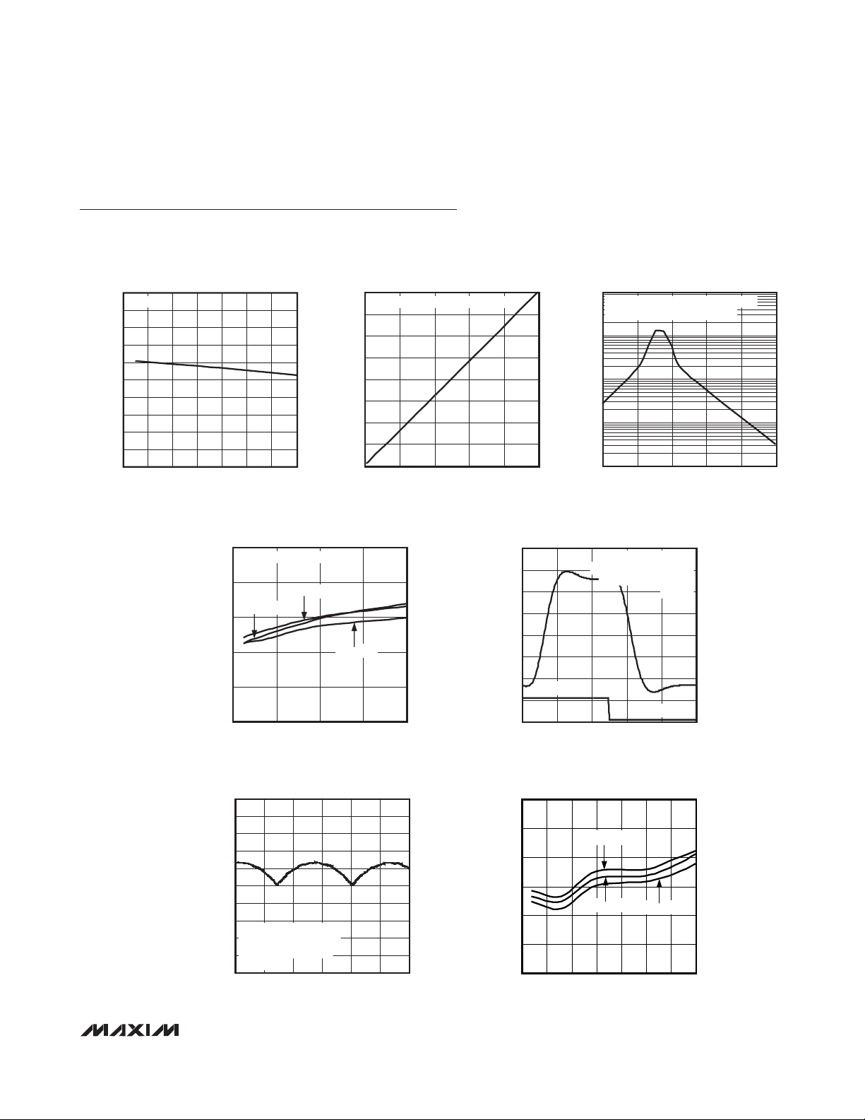
Typical Operating Characteristics
(V
DVDDIO
= +5V, V
AVDD
= +3.3V, V
DVDD
= +2.5V, f
SYSCLK
= 16MHz, burst frequency = bandpass frequency = 50kHz, TA= +25°C,
unless otherwise noted.)
BURST OUTPUT FREQUENCY
vs. TEMPERATURE
50.05
USING PLL
50.04
50.03
50.02
50.01
50.00
49.99
49.98
49.97
BURST OUTPUT FREQUENCY (kHz)
49.96
49.95
-50 125
TEMPERATURE (°C)
5025 100750-25
BANDPASS FILTER OUTPUT NOISE FLOOR
vs. BANDPASS FILTER CENTER FREQUENCY
15
RECEIVE PATH GAIN AT MAXIMUM
)
RMS
12
TA = +105°C
9
6
3
BANDPASS FILTER OUTPUT (LSB
0
20 100
LOWPASS FILTER OUTPUT RIPPLE vs. TIME
15,000
14,500
14,000
13,500
13,000
12,500
12,000
LPF OUTPUT (LSB)
11,500
MINIMUM ECHO GAIN
11,000
20mV
50kHz ECHO FREQUENCY
10,500
250ksps
10,000
012
65,536
57,344
MAXQ7667 toc01
49,152
40,960
32,768
24,576
LPF OUTPUT (LSB)
16,384
TA = +25°C
FREQUENCY (kHz)
ECHO AMPLITUDE
P-P
246 108
TIME (ms)
LOWPASS FILTER OUTPUT
vs. ECHO INPUT AMPLITUDE
PROGRAMMABLE ECHO GAIN = MINIMUM
8192
0
0 0.10
TA = -40°C
806040
0.040.02 0.080.06
ECHO INPUT AMPLITUDE (V
MAXQ7667 toc04
MAXQ7667 toc06
P-P
16,000
14,000
12,000
10,000
ADC COUNT (LSB)
OFFSET ERROR (mV)
LOWPASS FILTER OUTPUT
vs. ECHO INPUT FREQUENCY
100,000
PROGRAMMABLE ECHO GAIN = MINIMUM
ECHO INPUT AMPLITUDE = 20mV
MAXQ7667 toc02
10,000
1000
LPF OUTPUT (LSB)
100
10
25 100
)
ECHO INPUT FREQUENCY (kHz)
RECEIVE PATH RESPONSE TIME
(ECHO INPUT TO LOWPASS FILTER OUTPUT)
MINIMUM ECHO GAIN
ECHO AMPLITUDE
20mV
P-P
50kHz ECHO FREQUENCY
8000
6000
4000
2000
INPUT ON
0
0 1000
400200 800600
TIME (µs)
250ksps
INPUT OFF
SAR ADC OFFSET ERROR
vs. TEMPERATURE
2.0
1.5
1.0
0.5
0
-0.5
-1.0
-50 125
V
= 3.6V
AVDD
V
= 3.3V
AVDD
07525-25 10050
TEMPERATURE (°C)
V
AVDD
= 3V
P-P
MAXQ7667 toc03
5540 8570
MAXQ7667 toc05
MAXQ7667 toc07
Page 10
MAXQ7667
16-Bit, RISC, Microcontroller-Based,
Ultrasonic Distance-Measuring System
10 ______________________________________________________________________________________
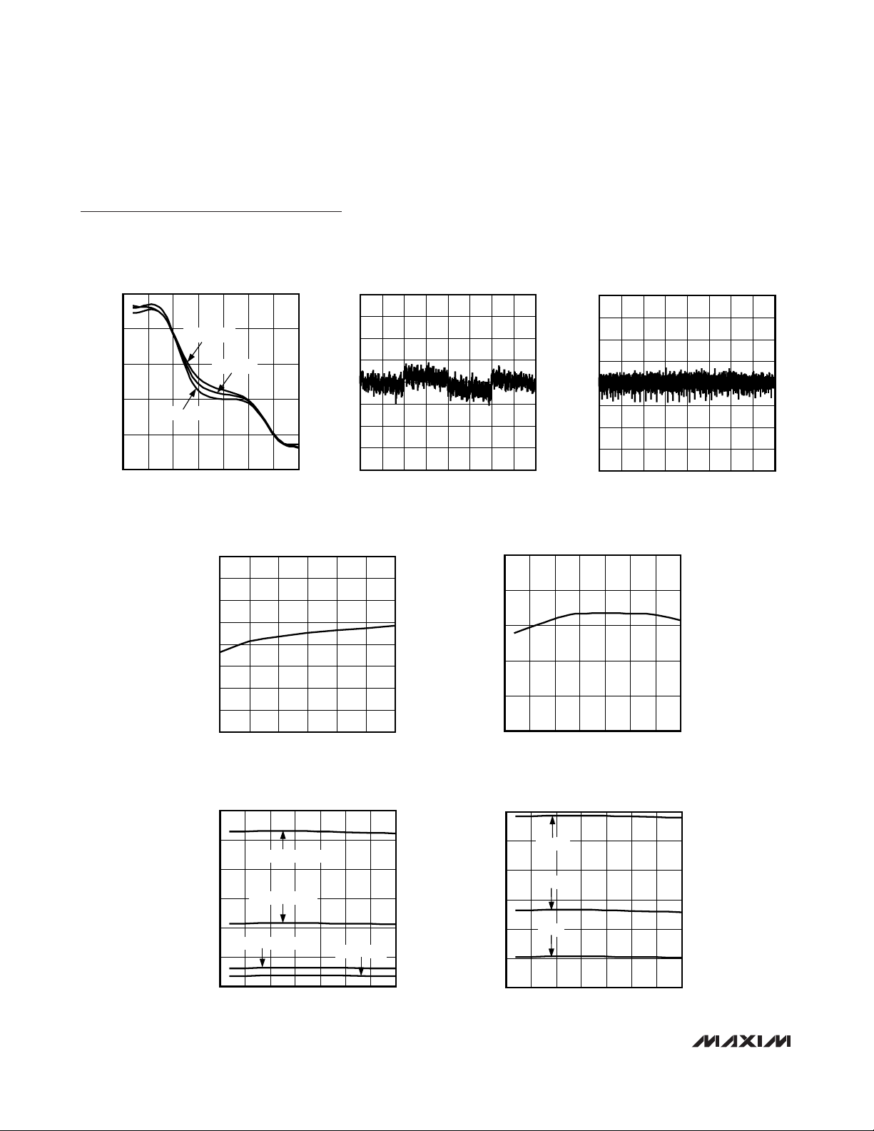
Typical Operating Characteristics (continued)
(V
DVDDIO
= +5V, V
AVDD
= +3.3V, V
DVDD
= +2.5V, f
SYSCLK
= 16MHz, burst frequency = bandpass frequency = 50kHz, TA= +25°C,
unless otherwise noted.)
GAIN ERROR (mV)
SAR ADC GAIN ERROR
vs. TEMPERATURE
3.0
2.5
2.0
1.5
1.0
0.5
-50 125
V
AVDD
V
= 3.6V
AVDD
07525-25 10050
TEMPERATURE (°C)
= 3.3V
V
AVDD
= 3V
MAXQ7667 toc08
INL (LSB)
-0.5
-1.0
-1.5
-2.0
SAR ADC INL vs. CODE
2.0
1.5
1.0
0.5
0
0409625601536512 3584
CODE
2.0
1.5
MAXQ7667 toc09
1.0
0.5
0
DNL (LSB)
-0.5
-1.0
-1.5
307220481024
-2.0
0 409625601536512 3584
SAR ADC DNL vs. CODE
MAXQ7667 toc10
307220481024
CODE
REFERENCE OUTPUT VOLTAGE
vs. SUPPLY VOLTAGE
2.520
2.519
2.518
2.517
2.516
2.515
REF OUTPUT VOLTAGE (V)
2.514
2.513
2.512
3.0 3.63.1 3.4
AVDD SUPPLY VOLTAGE (V)
SUPPLY BROWNOUT THRESHOLDS
vs. TEMPERATURE
5.0
4.5
4.0
3.5
3.0
SUPPLY THRESHOLD (V)
2.5
DVDDIO INTERRUPT
AVDD INTERRUPT
DVDD INTERRUPT
3.53.33.2
DVDD RESET
MAXQ7667 toc11
MAXQ7667 toc13
REFERENCE OUTPUT VOLTAGE
vs. TEMPERATURE
2.55
2.53
2.51
2.49
REF OUTPUT VOLTAGE (V)
2.47
2.45
-50 12550-25
025 10075
TEMPERATURE (°C)
REGULATOR OUTPUT VOLTAGE
vs. TEMPERATURE
5.0
4.5
4.0
3.5
3.0
REGULATOR OUTPUT VOLTAGE (V)
2.5
DVDDIO
AVDD
DVDD
MAXQ7667 toc12
MAXQ7667 toc14
2.0
-50 12550
TEMPERATURE (°C)
25 1000-25 75
2.0
25 1000-25 75-50 12550
TEMPERATURE (°C)
Page 11
MAXQ7667
16-Bit, RISC, Microcontroller-Based,
Ultrasonic Distance-Measuring System
______________________________________________________________________________________
11
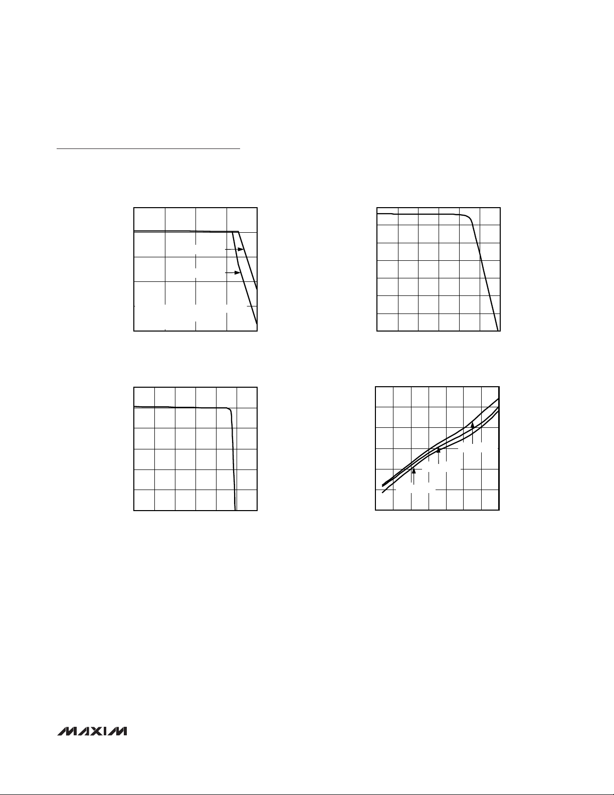
Typical Operating Characteristics (continued)
(V
DVDDIO
= +5V, V
AVDD
= +3.3V, V
DVDD
= +2.5V, f
SYSCLK
= 16MHz, burst frequency = bandpass frequency = 50kHz, TA= +25°C,
unless otherwise noted.)
DVDDIO REGULATOR OUTPUT VOLTAGE
5.5
5.0
4.5
4.0
3.5
EXTERNAL VOLTAGE SOURCE CONNECTED
TO THE DRAIN OF EXTERNAL PASS
DVDDIO REGULATOR OUTPUT VOLTAGE (V)
TRANSISTOR BSP129
3.0
0 200150
REG2P5 REGULATOR OUTPUT VOLTAGE
3.0
2.5
2.0
vs. LOAD CURRENT
DRAIN = 14V
DRAIN = 8V
10050
DVDDIO LOAD CURRENT (mA)
vs. LOAD CURRENT
REG3P3 REGULATOR OUTPUT VOLTAGE
vs. LOAD CURRENT
3.5
MAXQ7667 toc15
3.0
2.5
2.0
1.5
1.0
0.5
REG3P3 REGULATOR OUTPUT VOLTAGE (V)
0
0 12010020 80
REG3P3 LOAD CURRENT (mA)
6040
RC OSCILLATOR FREQUENCY
vs. TEMPERATURE
15.0
MAXQ7667 toc17
14.5
14.0
MAXQ7667 toc16
MAXQ7667 toc18
1.5
1.0
0.5
REG2P5 REGULATOR OUTPUT VOLTAGE (V)
0
012010020 80
REG2P5 LOAD CURRENT (mA)
6040
13.5
V
= 2.50V
V
= 2.75V
DVDD
07525-25 10050
TEMPERATURE (°C)
DVDD
13.0
RC OSCILLATOR FREQUENCY (MHz)
12.5
12.0
-50 125
V
DVDD
= 2.25V
Page 12
MAXQ7667
16-Bit, RISC, Microcontroller-Based,
Ultrasonic Distance-Measuring System
12 ______________________________________________________________________________________
Pin Description
PIN NAME FUNCTION
1 P1.3/TCK
2 P1.4/MOSI
3 P1.5/MISO
4 P1.6/SCLK
5 P1.7/SYNC/SS
6, 19, 42 DVDD
7, 18, 43 DGND Digital Ground. Connect all DGND nodes together. Connect to AGND at a si ngle point.
8, 17, 44 DVDDIO
9 P0.0/URX
10 P0.1/UTX
11 P0.2/TXEN
12
13 P0.4/T0B
14 P0.5/T1
15 P0.6/T2
16 P0.7/T2B
20 XIN
P0.3/T0/
ADCCTL
Port 1 Data 3/JTAG Serial Clock Input. P1.3 i s a general-purpose digital I/O. TCK is the JTAG
serial test clock input. Refer to the MAXQ7667 User’s Guide Sections 5 and 11.
Port 1 Data 4/SPI Serial Data Output. P1.4 is a general-purpose digital I/O. MOSI is the master
output, sla ve input for the SPI interface. Refer to the MAXQ7667 User’s Guide Sections 5 and 9.
Port 1 Data 5/SPI Serial Data Input. P1.5 is a general-purpose digital I/O. MISO is the ma ster input,
slave output for the SPI interface. Refer to the MAXQ7667 User’s Guide Sections 5 and 9.
Port 1 Data 6/SPI Serial Clock Output. P1.6 is a general-purpose digital I/O. SCLK is the serial
clock for the SPI interface. SCLK is an input when operating as a s lave and an output when
operating as a master. Refer to the MAXQ7667 User’s Guide Sections 5 and 9.
Port 1 Data 7/Schedule Timer Sync Input/SPI Slave Select. P1.7 is a general-purpose digital I/O.
A rising edge on the SYNC input resets the schedule timer. In SPI slave mode, SS is the SPI
slave-select input. In SPI master mode, use SS or a GPIO to manually select an external slave.
Refer to the MAXQ7667 User’s Guide Sections 5, 7, and 9.
Digital Supply Voltage. Connect DVDD directly to a +2.5V external source or to REG2P5 output for
single supply operation. B ypass DVDD to DGND with a 0.1µF capacitor as clo se a s possible to
the device. Connect all DVDD nodes together.
Digital I/O Supply Voltage. DVDDIO powers al l digital I/Os except for XIN and XOUT. Bypass
DVDDIO to DGND with a 0.1µF capacitor as close as possible to the device. Connect all DVDDIO
nodes together.
Port 0 Data 0/UART Rece ive Data Input. P0.0 is a general-purpose digital I/O. URX is a UART or
LIN data receive input. Refer to the MAXQ7667 User ’s Guide Sections 5 and 8.
Port 0 Data 1/UART Transm it Data Output. P0.1 i s a general-purpose digital I/O. UTX is a UART or
LIN data transmit output. Refer to the MAXQ7667 User’s Guide Sections 5 and 8.
Port 0 Data 2/UART Transm it Output. P0.2 is a general-purpose digital I/O. TXEN asserts low when
the UART is transmitting. Use TXEN to enable an e xternal LIN/UART transcei ver. Refer to the
MAXQ7667 U ser’ s Guide Sections 5 and 8.
Port 0 Data 3/Timer 0 I/O/ADC Control Input. P0.3 is a general-purpose digital I/O. T0 is the
primary Type 2 timer/counter 0 output or input. ADCCTL is a sampling/conversion trigger input for
the SAR ADC. Refer to the MAXQ7667 User ’s Guide Sections 5, 6, and 14.
Port 0 Data 4/Timer 0B I/O/Comparator Output. P0.4 is a general-purpose d igital I/O. T0B is the
secondary Type 2 timer/counter 0 output or input. Refer to the MAXQ7667 User’s Guide Sections
5 and 6.
Port 0 Data 5/Timer 1 I/O. P0.5 is a general-purpose digital I/O. T1 is the primary Type 2
timer/counter 1 output or input. Refer to the MAXQ7667 User’s Guide Sections 5 and 6.
Port 0 Data 6/Timer 2 I/O. P0.6 is a general-purpose digital I/O. T2 is the primary Type 2
timer/counter 2 output or input. Refer to the MAXQ7667 User’s Guide Sections 5 and 6.
Port 0 Data 7/Timer 2B I/O. P0.7 is a general-purpose digital I/O. T2B is the secondary Type 2
timer/counter 2 output or input. Refer to the MAXQ7667 User’s Guide Sections 5 and 6.
Crystal Oscillator Input. Connect an external crystal or resonator between XIN and XOUT. When
using an external clock source drive XIN with 2.5V level clock while leaving XOUT unconnected.
Connect XIN to DGND when an external clock source i s not used.
Page 13

MAXQ7667
16-Bit, RISC, Microcontroller-Based,
Ultrasonic Distance-Measuring System
______________________________________________________________________________________ 13
Pin Description (continued)
PIN NAME FUNCTION
Crystal Oscillator Output. Connect an external crystal or resonator between XIN and XOUT. Leave
21 XOUT
22 REG2P5 +2.5V Voltage Regulator Output
23 REG3P3 +3.3V Voltage Regulator Output
24 GATE5
25 RESET
26 FILT
27, 32 AVDD
28, 31, 33 AGND Analog Ground. Connect all AGND nodes together. Connect to DGND at a single point.
29 ECHON Negati ve Echo Input. AC-couple ECHON to an u ltrasonic transducer.
30 ECHOP Positive Echo Input. AC-couple ECHOP to an ultrasonic transducer.
34 REF
35 REFBG +2.5V Reference Output/Reference Buffer Input. Bypas s to AGND with a 0.47µF capacitor.
36 AIN0 SAR ADC Input 0. AIN0 pairs with AIN1 in differential mode.
37 AIN1 SAR ADC Input 1. AIN1 pairs with AIN0 in differential mode.
38 AIN2 SAR ADC Input 2. AIN2 pairs with AIN3 in differential mode.
49 AIN3 SAR ADC Input 3. AIN3 pairs with AIN2 in differential mode.
40 AIN4 SAR ADC Input 4
41 N.C. No Connection. Internally connected. Leave unconnected.
45 BURST
46 P1.0/TDO
47 P1.1/TMS
48 P1.2/TDI
XOUT unconnected when driving XIN with a 2.5V level clock or when an external clock source is
not used.
+5V DVDDIO Voltage Regulator Control Output. GATE5 controls an external npn or nMOS
transistor that pas ses power to DVDDIO.
Reset Input/Output. RESET is open drain with an internal pullup resistor to DVDDIO. Internal
circuitry pulls RESET low when V
enabled and the watchdog timeout period e xpires. Force RESET low externally for manual reset.
PLL VCO Control Input. Connect external filter components on FILT for the in ternal PLL circu it. See
the Typical Application Circuit/Functional Diagram.
Analog Supply Voltage. Connect all AVDD inputs directly to a +3.3V source or to REG3P3 for selfpowered operation. Bypass each AVDD to AGND with a 0.1µF capacitor as close as possible to
the device.
ADC Reference Input/Reference Buffer Output. When using the internal reference, the buffered
bandgap reference voltage (V
external reference, apply an e xternal vo ltage source ranging between 1V and V
Disable the reference buffer when apply ing an external reference at REF. B ypass REF to AGND
with a 0.47µF capacitor.
Burst Output. Burst is the ultrasonic transducer excitation pulse output. BURST remains in threestate mode on power-up.
Port 1 Data 0/ JTAG Output. P1.0 is a general-purpose digital I/O. TDO is the JT AG ser ial data
output. Refer to the MAXQ7667 User’s Guide Sections 5 and 11.
Port 1 Data 1/ JTAG Test Mode-Select Input. P1.1 is a general-purpose digital I/O. TMS is the JTAG
mode-select input. Refer to the MAXQ7667 User’s Guide Section s 5 and 11.
Port 1 Data 2/ JTAG Input. P1.2 i s a general-purpose digital I/O. TDI is the JTAG serial data input.
Refer to the MAXQ7667 User’s Guide Sections 5 and 11.
REF
fal ls b elow its brownout reset va lue or watchdog reset is
DVDDIO
) is provided for both SAR and sigma-delta ADCs. When using an
at REF.
AVDD
Page 14

MAXQ7667
16-Bit, RISC, Microcontroller-Based,
Ultrasonic Distance-Measuring System
14 ______________________________________________________________________________________
Typical Application Circuit/Functional Diagram
TRANSDUCER
0.01µF
470pF
0.01µF
470pF
BSP129
0.1µF
0.1µF
+8V TO
+20V
GND
LIN
V+
CONNECTOR
LIN
TRANSCEIVER
LIN
0.1µF
Rx
Tx
BURST
ECHON
ECHOP
DVDDIO
GATE5
REG3P3
AVDD
REG2P5
DVDD
DGND
GPIO/JTAG
P0.0/URX
P0.1/UTX
GPIO/SPI
0V
INTERFACE
MODULE
BURST ENABLE
2mV
P-P
AGND
POR/
BROWNOUT
LNA
BURST OUTPUT
DUTY CYCLE
AND PULSE
COUNTER
16 x 16
HW MULT
PLUS ACCUM
WATCHDOG
RESET
RAM
SIGMA-
DELTA
ADC
ROM
FLASH
13.5MHz
RC
OSCILLATOR
0.47µF
VOLTAGE
REFERENCE
DIGITAL
BANDPASS
FILTER
MAXQ20 RISC
OSCILLATOR
XIN XOUT
20pF
µC
MAXQ7667
CRYSTAL
16MHz
0.47µF
RECTIFIER
SCHEDULE
TIMER
20pF
FULLWAVE
REFREFBG
12-BIT
SAR ADC
DIGITAL
LOWPASS
FILTER
FIFO
PROGRAMMABLE
PLL
CLOCK PRESCALER
DIVIDE BY 1 TO 128
TIMER 2
PO.6/T2
PO.7/T2B
INTERRUPT
THRESHOLD
ADJUST
TIMER 1 TIMER 0
PO.3/T0/ADCCTL
PO.5/T1
PO.4/T0B
AIN0
AIN1
AIN2
AIN3
AIN4
FILT
330pF
AVDD
THERMISTOR
BATTERY+
24kΩ
33nF
Page 15

MAXQ7667
16-Bit, RISC, Microcontroller-Based,
Ultrasonic Distance-Measuring System
______________________________________________________________________________________ 15
Detailed Features
o Smart Analog Peripherals
Dedicated Ultrasonic Burst Generator
Echo Receiving Path
Low-Noise Amplifier
Time Variable Gain Amplifier
16-Bit Sigma-Delta ADC
Digital Bandpass Filter
Full-Wave Rectifier and Digital Lowpass Filter
8-Deep, 16-Bit Wide FIFO Simplifies Real-Time
Processing
Magnitude Comparator
5-Channel, 12-Bit SAR ADC with 250ksps
Sampling Rate
Internal Bandgap Voltage Reference for the ADCs
(Also Accepts External Voltage Reference)
o Timer/Digital I/O Peripherals
SPI Interface
Three 16-Bit (or Six 8-Bit) Programmable Type 2
Timers/Counters
16-Bit Schedule Timer
Programmable Watchdog Timer
16 General-Purpose Digital I/Os with
Multipurpose Capability
o High-Performance, Low-Power, 16-Bit RISC Core
1MHz–16MHz Operation, Approaching 1MIPS per
1MHz
Low Power (< 2.5mA/MIPS, DVDD = +2.5V)
16-Bit Instruction Word, 16-Bit Data Bus
33 Instructions (Most Require Only One Clock
Cycle)
16-Level Hardware Stack
Three Independent Data Pointers with Automatic
Increment/Decrement
o Program and Data Memory
Internal 32KB Program Flash
Internal 4KB Data RAM
Internal 8KB Utility ROM
o Crystal/Clock Module
1MHz–16MHz External Crystal Oscillator
13.5MHz Internal RC Oscillator
External Clock Source Operation
o 16 x 16 Hardware Multiplier with 48-Bit
Accumulator, Single Clock Cycle Operation
o Power-Management Module
Power-On Reset (POR)
Power-Supply Supervisor/Brownout Detection for
All Supplies
On-Chip +5V, +3.3V, and +2.5V Regulators for
Single Supply Operation
o JTAG Interface
Extensive Debug and Emulation Support
In-System Test Capability
Flash-Memory-Program Download
o UART
Synchronous and Asynchronous Transfers
Independent Baud-Rate Generator
2-Wire Interface
Transmit and Receive FIFOs
o LIN
Supports LIN 1.3, LIN 2.0, and SAE J2602
Automatic Baud-Rate Detection and LIN Frame
Synchronization
Up to 64 Bytes Frame Length
Automatic Calculation of Standard (LIN 1.3) and
Enhanced (LIN 2.0) Checksums
o 7mm x 7mm, 48-Pin LQFP Package
o -40°C to +125°C Operating Temperature Range
Page 16

MAXQ7667
16-Bit, RISC, Microcontroller-Based,
Ultrasonic Distance-Measuring System
16 ______________________________________________________________________________________
Detailed Description
The ultrasonic distance-measurement peripherals in the
MAXQ7667 include a burst signal generator for
acoustic transmission and mixed signal circuits for
amplifying and digitizing echo signals ranging between
25kHz and 100kHz. The burst signal is a square wave
with adjustable duty cycle and pulse count. The burst is
derived either directly from the system clock or from a
programmable PLL locked to the system clock. The
MAXQ7667 effectively digitizes the echo signals
received at the ECHOP and ECHON inputs using an
LNA, sigma-delta ADC with variable analog gain amplifier, noise-limiting digital bandpass filter, digital fullwave rectifier, and a digital lowpass filter (see the
Typical Application Circuit/Functional Diagram
). The
device detects echo signals at the burst frequency with
amplitudes ranging from 10µV
P-P
to 100mV
P-P
. Echoes
greater than 100mV
P-P
and less than 2V
P-P
are internally clipped but do not saturate the receiver. To optimize
echo reception, the clock used for processing the echo
locks to the burst frequency. The MAXQ7667’s burst
generator can generate higher frequencies, but the
maximum usable frequency for the echo receive path is
100kHz . For applications requiring transducer frequencies above 100kHz, implement an external echo
receive path. The SAR ADC can then digitize the filtered echo envelope.
An integrated 16-bit RISC µC (MAXQ20) provides timing control, signal processing, and data I/O. The 16-bit
Harvard architecture RISC core executes most instructions in a single clock cycle from instruction fetch to
cycle completion. The MAXQ20 provides optimal performance for noise-sensitive analog applications.
The MAXQ7667 includes a 13.5MHz RC oscillator,
external crystal oscillator, watchdog timer, schedule
timer, three general-purpose Type 2 timers/counters,
two 8-bit GPIO ports, SPI interface, JTAG interface, LIN
capable UART interface, 12-bit SAR ADC with five multiplexed input channels, supply-voltage monitors, and a
voltage reference for communication, diagnostics, and
miscellaneous support.
Burst Controller
The MAXQ7667 provides a square-wave burst signal at
the BURST output. Use the burst control to transmit an
ultrasonic signal. Typical applications use the burst signal to switch an external transistor that drives a highvoltage transformer, which excites the transducer (see
the
Typical Application Circuit/Functional Diagram
).
Use software to configure the duty cycle, frequency,
number of pulses, and drive current of the burst. See
Section 17 of the
MAXQ7667 User’s Guide
.
Derive the burst signal either directly from the system
clock or from a programmable oscillator phase locked
to the system clock (Figure 1). Using the system clock
limits the burst frequency to one of 16 choices. Integer
division of the system clock generates these 16 frequencies. The PLL allows a fractional division of the
system clock. Any frequency within the PLL range is
selectable to a resolution of 0.13% or better.
When using the internal PLL, connect external filter
components (C1, R1, and C2) to FILT as shown in
Figure 1. These components filter the analog voltage
that controls the VCO in the PLL. The filter component
values shown in the figure are suitable for the entire
PLL frequency range.
MAXQ7667
C2
330pF
SYSTEM
CLOCK
(f
SYSCLK
)
ECHO
RECEIVE
CLOCK
PLL
C1
33nF
FILT
R1
24kΩ
PWM
2mV
P-P
DIAGNOSTIC
BURST
1
0
BTRN.10:BCKS
BPH[9:0]
PLLF[10:9]:PLLC[1:0]
BTRN[15:12]:BDIV[3:0]
BTRN[7:0]:BCNT[7:0]
BPH.15:BSTT
BTRN.9:BTRI
BPH.14:BDSBTRN.11:BPOL
BTRN.8:BGT
BURST
PLLF[8:0]
BURST CLOCK
GENERATOR
RECEIVE CLOCK
PRESCALE
Figure 1. Burst Transmission Stage
Page 17

MAXQ7667
Echo Receive Path
Low-Noise Amplifier (LNA)
The LNA provides a 40V/V fixed gain to the input signal.
The differential inputs of the LNA are ECHOP and
ECHON. For proper biasing of the LNA, AC-couple the
transducer or any external circuitry to ECHOP and
ECHON. For a single-ended input signal, AC-couple the
signal to ECHOP with a 0.01µF capacitor and connect
ECHON to AGND through a 0.01µF capacitor placed as
close as possible to the signal source. The outputs of the
LNA connect to the inputs of a 16-bit sigma-delta ADC
and can connect internally to the AIN0 and AIN1 inputs
of the SAR ADC for external monitoring (Figure 2).
Diagnostic Signals
An analog multiplexer located at the input of the LNA
selects one of three possible signals for processing by
the echo receive path; the normal echo signal AC-coupled to the ECHOP and ECHON inputs, 0V signal, or a
2mV
P-P
internally generated signal (Figure 2). The
2mV
P-P
square-wave signal, with frequency and duty
cycle matching the burst signal, allows the echo
receive chain to process a simulated echo.
MAXQ7667
0.47µF
AGND
REFGB
0.47µF
TO EXTERNAL VOLTAGE
REFERENCE
AGND
REF
VARIABLE
GAIN SIGMA-
DELTA ADC
FIFO
8 x 16
FIFO
CONTROL
BANDPASS
FILTER
CLOCK
CONTROL
ECHO
RECEIVE
CLOCK
RCVC[4:0]:RCVGN[4:0]
RCVC[7:6]:LNAISEL[1:0]
RCVC.8:LNAOSEL
BPFI[15:0]
APE.13:RSARE
2.5V
BANDGAP REF
APE.12:BGE
FULL-WAVE
RECTIFIER PLUS
LOWPASS FILTER
R*
R*
*R = ECHO INPUT RESISTANCE. SEE THE ELECTRICAL CHARACTERISTICS SECTION.
40R*
AIN0
TO SAR ADC
AIN1
0V
2mV
P-P
40R*
LNA
AVDD/2
ECHOP
ECHON
MUX
BPFO[15:0]
LPFD[15:0]
CMPC[14:0]:CMPH[14:0]
CMPT[15:0]
LPFC[15:12]:FFIL[3:0]
LPFC[2.0]:FFLS[2:0]
LPFC.7:FFOV
ASR.2:LPFFL
LPFC[11:8]:FFDP[3:0]
CMPC.15:CMPP
ASR.12:CMPLVL
AIE.3:CMPIE
LPFF[15:0]
ASR.3:CMPI
COMPARATOR
AIE.1:LPFIE
ASR.1:LPFRDY
LPFC.3:FFLD
TIMER 0
TIMER 1
TIMER 2
DATA READY
INTERRUPT
AIE.2:LFLIE
Figure 2. Echo Receive Path
16-Bit, RISC, Microcontroller-Based,
Ultrasonic Distance-Measuring System
______________________________________________________________________________________ 17
Page 18

MAXQ7667
16-Bit, RISC, Microcontroller-Based,
Ultrasonic Distance-Measuring System
18 ______________________________________________________________________________________
Sigma-Delta ADC
The MAXQ7667 features a 16-bit sigma-delta ADC with
an analog gain adjustable from 38dB to 60dB (including the fixed LNA gain) with a maximum gain step of
12.5% (typical). Gain changes settle within one ADC
conversion. Use software to create a virtual time variable gain amplifier. A digital bandpass and lowpass filters remove switching glitches and DC offset at the
output of the ADC.
In a typical application, the software sets the gain to a
low value when the burst is first sent and increases the
gain as the time from when the burst was sent increases. As a result, strong echoes from nearby objects are
processed without clipping while small signals from distant objects are processed with the maximum gain. The
ADC samples the amplified echo signal from the LNA at
80 times the burst output frequency. The ADC provides
conversion results at a data rate equal to 10 times the
burst output frequency. The ADC conversion results
also load to an 8-deep first-in-first-out (FIFO) at the
native data rate or a separate time base without loading
the CPU.
Digital Bandpass Filter
The digital bandpass filter has a center frequency that
tracks the burst output frequency. The bandpass width
is 14% of the center frequency. The bandpass filter provides the 16-bit output data at a data rate equal to 10
times the burst output frequency.
Full-Wave Rectifier
The full-wave rectifier detects the envelope of the digital
bandwidth filter output to generate a DC output proportional to the peak-to-peak amplitude of the input signal.
Full-wave rectification allows the digital lowpass filter to
respond faster without excessive ripple.
Digital Lowpass Filter
The lowpass filter removes the ripple from the full-wave
detector output. The output of the lowpass filter is available at a data rate equal to five times the burst output
frequency. The corner frequency is 1/5 the burst frequency with approximately 40dB per decade rolloff.
The 16-bit output data of the lowpass filter is stored in a
FIFO register with a depth of eight samples. The
MAXQ7667 allows data transfer from the lowpass filter
SARC[2:0]:SARS[2:0]
SARC[11:9]:SARMX[2:0]
REFERENCE TO
SIGMA-DELTA ADC
ADC DATA
READY INTERRUPT
ASR.0:SARRDY
APE.12:BGE
APE.14:RBUFE
AIE.0:SARIE
BANDGAP
REF
SARC.3:SARBY
SARC.6:SARDUL
SARC.4:SARASD
SARC.7:SARBIP
SARC.8:SARDIF
OSCC[3:2]:SARCD[1:0]
ADC
CLOCK
DIV
TIMER 0
TIMER 1
TIMER 2
APE.4:SARE ADCCLK
AVDD
V
REF
MUX
SARC[11:9]:SARMX[2:0]
12-BIT
ADC
AIN0
MUX
AIN1
AIN2
AIN3
DATA BUS[15:0]
AIN4
V
REF
AGND
AVDD
AGND
REFBG
ADCCTL
REF
SYSCLK
BUF
x1.0
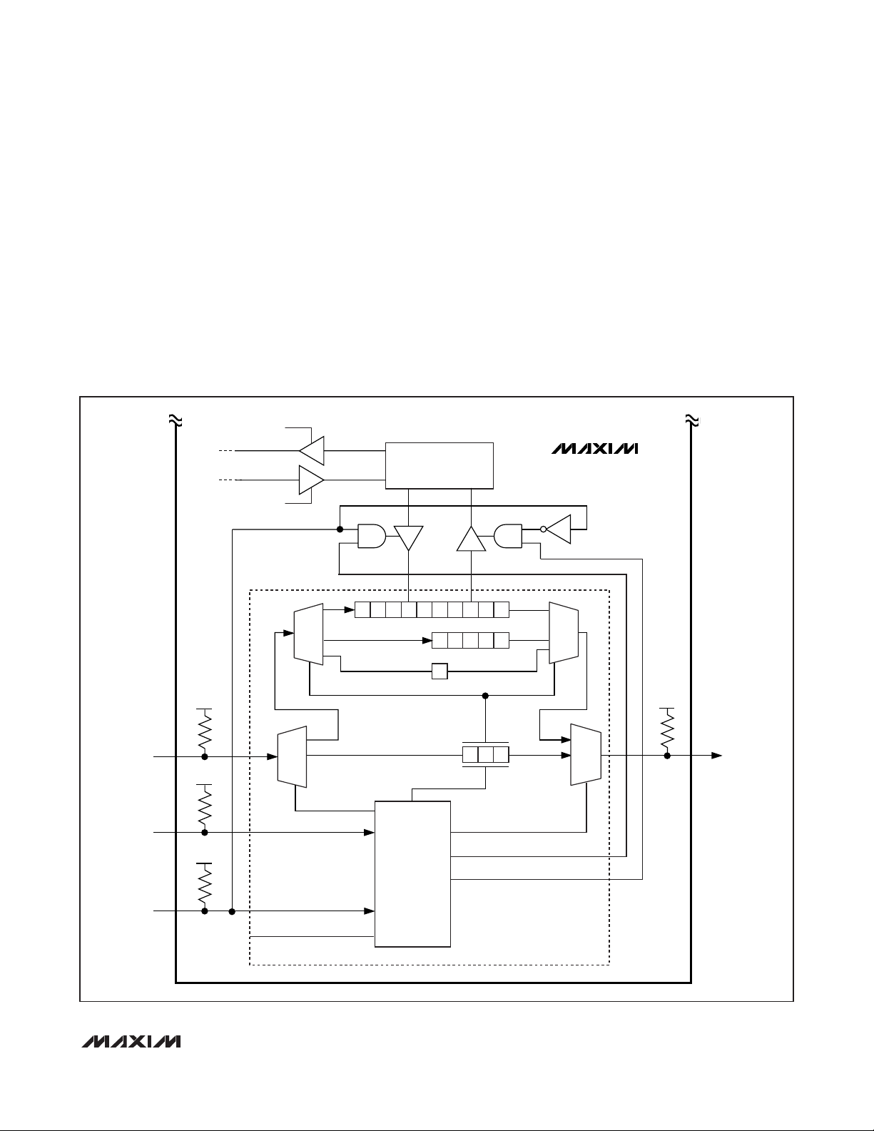
Figure 3. SAR ADC Block Diagram
Page 19
MAXQ7667
16-Bit, RISC, Microcontroller-Based,
Ultrasonic Distance-Measuring System
______________________________________________________________________________________ 19
output to the FIFO automatically each time the lowpass
filter output updates, through the control of one of the
timer outputs, or through software. The device includes
a FIFO depth counter with programmable interrupt levels and generates an interrupt if a FIFO overflow condition occurs. The output of the digital lowpass filter
connects to a digital comparator that can generate an
interrupt for a specified echo signal level.
Digital Comparator and Threshold Adjust
The digital comparator output asserts when the echo
amplitude at the output of the digital lowpass filter crosses a given threshold. The comparator’s threshold level,
hysteresis, and interrupt polarity are programmable.
SAR ADC
The MAXQ7667 incorporates a 12-bit unbuffered SAR
ADC with sample-and-hold and conversion rate up to
250ksps. The ADC allows measurements of tempera-
ture, battery voltage, or other parameters using five single-ended or two fully differential analog inputs
(AIN0–AIN4). All of the analog inputs have a range of 0
to V
REF
in unipolar mode and ±V
REF
/2 in bipolar mode.
The SAR ADC supports three different conversion start
sources: timers, ADC control input (ADCCTL), and software write. The conversion start source triggers the
ADC acquisition and conversion. The system clock provides the ADC clock frequency programmable to 1/2,
1/4, 1/8, or 1/16 of the system clock. Use internal
bandgap reference, external reference, or AVDD for
voltage reference of the SAR ADC. Figure 3 shows a
simplified block diagram of the SAR ADC.
The output of the SAR ADC is straight binary in unipolar
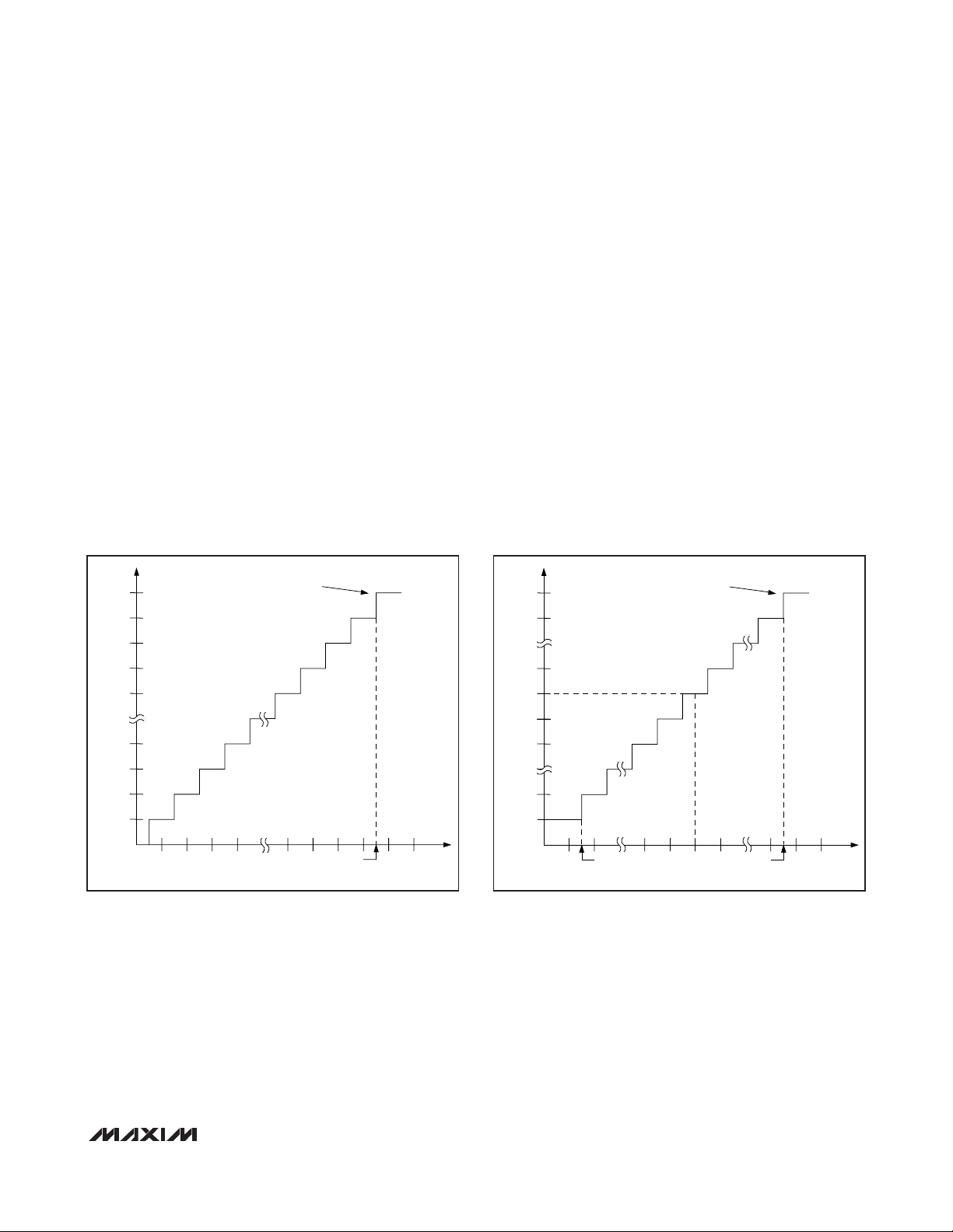
mode and two’s complement in bipolar mode. Figures 4
and 5 show the ADC transfer functions in unipolar
mode and bipolar mode.
000
001
002
003
004
FFC
FFB
FFD
FFE
FFF
0123
4
FS
FS - 1.5 LSB
FULL-SCALE
TRANSITION
FS = REF
ZS = 0
1 LSB = REF/4096
OUTPUT CODE (hex)
DIFFERENTIAL INPUT VOLTAGE (LSB)
Figure 4. Unipolar Transfer Function
800
801
FFE
001
000
FFF
7FE
7FF
-FS
0
+FS
OUTPUT CODE (hex)
DIFFERENTIAL INPUT VOLTAGE (LSB)
+FS - 1.5 LSB
FULL-SCALE
TRANSITION
+FS = REF/2
ZS = 0
-FS = -REF/2
1 LSB = REF/4096
-FS + 0.5 LSB
Figure 5. Bipolar Transfer Function
Page 20

MAXQ7667
16-Bit, RISC, Microcontroller-Based,
Ultrasonic Distance-Measuring System
20 ______________________________________________________________________________________
SAR ADC Analog Input Track-and-Hold (T/H)
Figures 6 and 7 show the equivalent input circuit of the
MAXQ7667 analog input architecture. During acquisition (track), a sampling capacitor charges to the positive input voltage at AIN0–AIN4 in single-ended mode
or AIN0 and AIN2 in differential mode while a second
sampling capacitor connects to AGND in single-ended
mode or AIN1 and AIN3 in differential mode. The ADC
conversion start source and the ADC dual mode selection bits control the T/H timing.
Voltage Reference
The MAXQ7667 supports three possible voltage reference sources for ADC conversion; 2.5V internal
buffered bandgap reference, external source, and
AVDD. The internal 2.5V bandgap reference has high
initial accuracy and temperature coefficient of typically
less than 100ppm/°C. When operating in internal reference mode, either the buffered output of the internal
reference or AVDD connects to the SAR ADC while the
buffered output of the internal reference connects to the
sigma-delta ADC. When operating in external reference
mode, an external source ranging between 1V and
V
AVDD
applied at either the REF or REFBG inputs pro-
vides the reference to the SAR ADC and sigma-delta
ADC. Bypass REFBG and REF to AGND with a 0.47µF
capacitor for optimum performance. See Section 14 of
the
MAXQ7667 User’s Guide
.
Schedule Timer
The MAXQ7667’s schedule timer provides general timekeeping and software synchronization to an external I/O.
The schedule timer features include the following:
• 16-bit autoreload up-counter for the timer
• Programmable 16-bit alarm register
• Alarm interrupts
• Schedule timer incremented by a programmable
system clock prescaler (1, 1/2, 1/4, 1/8, 1/16, 1/32,
1/64, 1/128)
• Schedule timer up-counter resettable through an
external I/O pin, which allows synchronization of a
schedule timer to an external event
• Wake-up alarm to pull the system clock from stopmode to normal operation
Figure 8 shows a simplified block diagram of the
schedule timer.
AGND
AIN+
AIN-
C
IN+
AVDD
C
IN-
R
IN+
R
IN-
Figure 6. Equivalent Input Circuit (Track/Acquisition Mode)
AGND
AIN+
AIN-
C
IN+
C
IN-
R
IN+
R
IN-
AVDD
Figure 7. Equivalent Input Circuit (Hold/Conversion Mode)
Page 21

MAXQ7667
16-Bit, RISC, Microcontroller-Based,
Ultrasonic Distance-Measuring System
______________________________________________________________________________________ 21
MAXQ is a registered trademark of Maxim Integrated Products, Inc.
Type 2 Timers/Counters
The MAXQ7667 includes three 16-bit timers/counters
with programmable I/O (Figure 9). Each timer is a Type
2 timer implemented in the MAXQ®family. The Type 2
timer is an autoreload 16-bit timer/counter offering the
following functions:
• 8-bit/16-bit timer/counter
• Up/down autoreload
• Counter function of external pulse
• Capture
• Compare
Clock Sources
The MAXQ7667 oscillator module supplies the system
clock for the µC core and all of the peripheral modules.
The high-frequency oscillator operates with a 1MHz to
16MHz crystal. Use the internal RC oscillator as the
system clock for applications that do not require precise timing. See Section 15 of the
MAXQ7667 User’s
Guide
.
The MAXQ7667 supports the following master clock
sources:
• Internal high-frequency oscillator drives an external 1MHz–16MHz crystal or ceramic resonator
• Internal, fast-starting, 13.5MHz RC oscillator
(default oscillator at startup and in the event the
external crystal fails)
• External 4MHz–16MHz clock input
Crystal Selection
The MAXQ7667 requires a crystal with the following
specifications:
Frequency: 1MHz–16MHz
C
LOAD
: 6pF (min)
Drive level: 5µW
Series resonance resistance: 30Ω (max)
Note: Quartz crystal vendors often specify series resonance resistance (R1). Series resonance resistance is
the resistance observed when the resonator is in the
series resonant condition. When a resonator is used in
the parallel resonant mode with an external load capacitance, as is the case with the MAXQ7667 oscillator circuit, the effective resistance at the loaded frequency of
oscillation is:
R1 x (1 + (CO/C
LOAD
))
2
For typical shunt capacitance (CO) and load capacitance (C
LOAD
) values, the effective resistance poten-
tially exceeds R1 by a factor of 2.
Page 22

MAXQ7667
16-Bit, RISC, Microcontroller-Based,
Ultrasonic Distance-Measuring System
22 ______________________________________________________________________________________
Figure 9. Type 2 Timer/Counter in 16-Bit Mode
PROGRAMMABLE
DIVIDE BY
1, 2, 4, ..., 128
COMPARATOR
STIM = SALM
SALM
REGISTER
SALM[15:0]
STIM
16-BIT UP-
COUNTER
SCNT.11:STDIV2
SCNT.0:STIME
CLR
CLR
SCHEDULE TIMER
SYSTEM
CLOCK
MAXQ7667
SCNT.8:SSYNC_EN
SCNT.7:SALIE
SCNT.1:SALME
INT
AN INTERRUPT IS
GENERATED WHEN
SALIE = 1 AND
SALMF = 1
SCNT.6:SALMF
STIM[15:0]
P1.7/SYNC
Figure 8. Schedule-Timer Module Block Diagram
CAPTURE
INPUT CONDITIONING
SCALING
GATING
CLOCK
T2Cx REGISTER
16-BIT CAPTURE/COMPARE
T2Vx REGISTER
16-BIT UP-COUNTER
T2Rx REGISTER
16-BIT RELOAD
OVERFLOW
RELOAD
EQUAL
OUTPUT CONDITIONING
POLARITY SELECTION
Page 23
MAXQ7667
16-Bit, RISC, Microcontroller-Based,
Ultrasonic Distance-Measuring System
______________________________________________________________________________________ 23
Figure 10. JTAG Interface Block Diagram
JTAG Interface
The joint test action group (JTAG) IEEE 1149.1 standard
defines a unique method for in-circuit testing and programming. The MAXQ7667 conforms to this standard,
implementing an external test access port (TAP) and
internal TAP controller for communication with a JTAG
bus master, such as an automatic test equipment (ATE)
system. The MAXQ7667 JTAG interface does not allow
boundary scan. For detailed information on the TAP and
TAP controller, refer to IEEE Std 1149.1 “IEEE Standard
Test Access Port and Boundary-Scan Architecture” on
the IEEE website at www.standards.ieee.org.
The TAP controller communicates synchronously with
the host system (bus master) through four digital I/Os:
test mode select (TMS), test clock (TCK), test data
input (TDI), and test data output (TDO). The internal
TAP module consists of shift registers and a TAP controller (Figure 10). The shift registers serve as transmit
and receive data buffers for a debugger. Maintain the
maximum TCK clock frequency to below 1/8 the system
clock frequency for proper operation.
READ
TO DEBUG
ENGINE
WRITE
MUX
SHADOW REGISTER
765432 10S1S0
DEBUG REGISTER
SYSTEM PROGRAMMING REGISTER
MAXQ7667
43210
MUX
DVDDIO
P1.2/TDI
DVDDIO
P1.1/TMS
DVDDIO
P1.3/TCK
POWER-ON
RESET
MUX
BYPASS
INSTRUCTION REGISTER
TAP
CONTROLLER
2
10
UPDATE-DR
UPDATE-DR
MUX
DVDDIO
P1.0/TDO
Page 24

MAXQ7667
16-Bit, RISC, Microcontroller-Based,
Ultrasonic Distance-Measuring System
24 ______________________________________________________________________________________
The following four digital I/Os form the TAP interface:
• TDO—Serial output signal for test instruction and
data. Data transitions on the falling edge of TCK.
TDO idles high when inactive. TDO serially transfers internal data to the external host. Data transfers lease significant bit first.
• TDI—Serial input signal for test instruction and
data. Transition data on the rising edge of TCK.
TDO pulls high when unconnected. TDI serially
transfers data from the external host to the internal
TAP module shift registers. Data transfers least
significant bit first.
• TCK—Serial clock for the test logic. When TCK
stops at 0, storage elements in the test logic must
retain their data indefinitely. Force TCK high when
inactive.
• TMS—Test mode selection. The rising edge of TCK
samples the test signals at TMS. The TAP controller
decodes the test signals at TMS to control the test
operation. Force TMS high when inactive.
UART/LIN Interface
The MAXQ7667 includes a UART/LIN transceiver combination that supports communication speeds up
2MBd. The LIN standard for example limits communication speed to 20kBd or less. Connect a LIN transceiver
or other UART connections such as RS-232 and RS-485
directly to the MAXQ7667’s 2-wire interface: URX and
UTX. The MAXQ7667 operates as a LIN slave or LIN
master device. The UART provides the programmable
baud-rate generators to communicate effectively to or
from the LIN transceiver. The device holds up to 8
bytes of data in each of the transmit and receive FIFOs.
The following characteristics apply to the MAXQ7667
UART/LIN interface:
• Full-duplex operation for asynchronous data transfers up to 500kBd (system clock/32)
• Half-duplex operation for synchronous data transfers up to 2MBd (system clock/8)
• 8-deep receive and transmit FIFO with programmable interrupt for receive and transmit
• Independent baud-rate generator
• Programmable 9th data bit (commonly used for
parity or address/data selection)—UART mode
only
• Hardware support for LIN including break detection, autobaud, address identity filtering, checksum calculation, and block length checking
• Supports common RS-232 and LIN baud rates:
1000, 1200, 2400, 4800, 9600, 19,200, 20,000,
38,400, 57,600, and 115,200 with system clock =
16MHz.
SPI Interface
The MAXQ7667 supports 4-wire SPI interface communication with 8-bit or 16-bit data streams operating in
either master mode or slave mode. The SPI interface
allows synchronous half-duplex or full-duplex serial
data transfers to a wide variety of external serial
devices using MISO, MOSI, SS, and SCLK signals.
Collision detection is provided when two or more masters attempt a data transfer at the same time. See
Section 9 of the
MAXQ7667 User’s Guide
.
General-Purpose Digital I/O Ports
Two 8-bit digital I/O ports (P0._ and P1._), with dedicated one or more alternative functions, are available as
general-purpose I/Os (GPIOs) under the control of the
integrated MAXQ20. Set each I/O within each port individually as an input or output. The GPIOs incorporate a
Schmitt trigger receiver and a full CMOS output driver
(Figure 13). Each GPIO configures as an input with
pullup to DVDDIO at power-up. When programmed as
an input, each I/O is configurable for high-impedance,
weak pullup to DVDDIO or pulldown to DGND. When
programmed as an output, writing to the port output
register (PO) controls the output logic state. The outputs source or sink at least 1.6mA. Configure the drive
strength for each I/O within each port to high or low
using the pad drive strength register for optimum EMI
performance. All the I/O ports have interrupt capability
that wake up the device while in stop mode and have
protection circuitry to DVDDIO and DGND.
Supply-Voltage Regulators
The MAXQ7667 requires three different power-supply
voltages. DVDDIO, nominally +5V, allows interfacing to
standard 5V logic on all the digital I/Os including the
LIN/UART, JTAG, and SPI ports. DVDD, nominally
+2.5V, powers all the high-speed digital circuits. AVDD,
nominally 3.3V, powers the analog circuits.
External power supplies or internal voltage regulators
provide each of the supply voltages. The internal voltage regulators provide 3.3V and 2.5V supplies from the
5V DVDDIO input. Obtain the 5V supply from a higher
external voltage supply by using a few external components. The MAXQ7667 includes an internal error amplifier used to regulate the voltage on DVDDIO by driving
the gate or base of an external pass transistor. Refer to
the
MAXQ7667 User’s Guide
for more details on the
external components needed for 5V regulation.
Page 25

MAXQ7667
16-Bit, RISC, Microcontroller-Based,
Ultrasonic Distance-Measuring System
______________________________________________________________________________________ 25
Figure 11. SPI Timing Diagram in Master Mode
Figure 12. SPI Timing Diagram in Slave Mode
SHIFT SAMPLE SHIFT
SS
SCLK
CKPOL/CKPHA
0/1 OR 1/0
SCLK
CKPOL/CKPHA
0/0 OR 1/1
MOSI
MISO
MSB
t
MIS
MSB
SHIFT SAMPLE SHIFT SAMPLE
t
SS
SCLK
CKPOL/CKPHA
0/1 OR 1/0
SCLK
CKPOL/CKPHA
0/0 OR 1/1
SSE
t
SCK
t
SIS
t
MCK
SAMPLE
t
MCH
t
MOH
t
SCH
t
MCL
t
MLH
LSB
LSB
t
SSH
t
SD
MSB - 1
t
MOV
t
MIH
MSB - 1
t
SCL
t
SIH
MOSI
MISO
MSB LSBMSB - 1
MSB
t
SOV
MSB - 1
Page 26

MAXQ7667
16-Bit, RISC, Microcontroller-Based,
Ultrasonic Distance-Measuring System
26 ______________________________________________________________________________________
Connect bypass capacitors at each power-supply input
as close as possible to the device. Use a bypass
capacitor less than 0.47µF on DVDDIO. For most applications, 0.1µF bypass capacitors are adequate.
Supply Brownout Monitor
Power supplies DVDD, AVDD, and DVDDIO each
include a brownout monitor/supervisor that alerts the
µC when their corresponding supply voltages drop
below the interrupt threshold. Activate each brownout
monitor independently using the corresponding
brownout enable bits: VDBE, VIBE, and VABE.
Reset
In reset mode, no instruction execution occurs and all
inputs/outputs return to their default states. Code execution resumes at address 8000h (in the utility ROM)
once the reset condition is removed.
Four different sources reset the MAXQ7667: POR,
watchdog timer reset, external reset, and internal system reset.
During normal operation, force RESET low for at least
four system clock cycles for an external reset. Set the
ROD bit in the SC register, while the SPE bit in the ICDF
register is set, for an internal system reset. See Section
16 of the
MAXQ7667 User’s Guide
.
Power-On Reset (POR)
The MAXQ7667 includes a DVDD voltage supervisor to
control the µC POR. On power-up, internal circuitry
pulls RESET low and resets all the internal registers.
RESET is held low for the duration of the power-on
delay after V
DVDD
rises above the DVDD reset threshold. The internal RC oscillator starts up and software
execution begins at the reset vector location 8000h
immediately after the device exits POR while RESET is
I/O PAD
DVDDIO
P0._
100ΩK
100ΩK
DGND
DGND
EIE0._
EIES0._
DETECT
CIRCUIT
INTERRUPT
FLAG
PS0._
PR0._
PD0._
PO0._
SF DIRECTION
SF ENABLE
SF OUTPUT
PI0._ OR
SF INPUT
FLAG
MUX
MUX
MAXQ7667
Figure 13. Port 0 Digital I/O Basic Circuitry. Port 1 Circuitry is the Same as Port 2.
Page 27

MAXQ7667
16-Bit, RISC, Microcontroller-Based,
Ultrasonic Distance-Measuring System
______________________________________________________________________________________ 27
not externally forced low. An internal POR flag indicates
the source of a reset. Ramp up the DVDD supply at a
minimum rate of 60mV/ms to keep the device in POR
until DVDD fully settles.
Watchdog Timer
The primary function of the watchdog timer is to watch
for stalled or stuck software. The watchdog timer performs a controlled system restart when the µP fails to
write to the watchdog timer register before a selectable
timeout interval expires. The internal 13.5MHz RC oscillator drives the MAXQ7667’s watchdog timer.
Figure 14 shows the watchdog timer functions as the
source of both the watchdog interrupt and watchdog
reset. The watchdog interrupt timeout period is programmable to 212, 215, 218, or 221cycles of the RC
oscillator resulting in a nominal range of 273µs to
139.8ms. The watchdog reset timeout period is a fixed
512 RC clock cycles (34µs). When enabled, the watchdog generates an interrupt upon expiration; then, if not
reset within 512 RC clock cycles, the watchdog asserts
RESET low for eight RC clock cycles.
Hardware Multiplier/Accumulator
A hardware multiplier supports high-speed multiplications. The multiplier completes a 16-bit x 16-bit multiplication in a single clock cycle and contains a 48-bit
accumulator. The multiplier is a peripheral that performs seven different multiplication operations:
• Unsigned 16-bit multiplication
• Unsigned 16-bit multiplication and accumulation
• Unsigned 16-bit multiplication and subtraction
• Signed 16-bit multiplication
• Signed 16-bit multiplication and negation
• Signed 16-bit multiplication and accumulation
• Signed 16-bit multiplication and subtraction
MAXQ Core Architecture
The MAXQ20 µC is an accumulator-based Harvard
memory architecture. Fetch and execution operations
complete in one clock cycle without pipelining because
the instruction contains both the op code and data. The
µC streamlines 16 million instructions per second
(MIPS). Integrated 16-level hardware stack enables fast
subroutine calling and task switching. Manipulate data
quickly and efficiently with three internal data pointers.
Multiple data pointers allow more than one function to
access data memory without having to save and
restore data pointers each time. The data pointers automatically increment or decrement following an operation, eliminating the need for software intervention.
Instruction Set
The instruction set consists of a total of 33 fixed-length
16-bit instructions that operate on registers and memory locations. The highly orthogonal instruction set allows
arithmetic and logical operations to use any register
along with the accumulator. System registers control
functionality common to all MAXQ µCs, while peripheral
registers control peripherals and functions specific to
the MAXQ7667. All registers are subdivided into register modules.
The architecture is transport-triggered. Writes or reads
from certain register locations potentially have side
effects. These side effects form the basis for the higher
level op codes defined by the assembler, such as
ADDC, OR, JUMP, etc. The op codes are implemented
as MOVE instructions between system registers. The
assembler handles all the instruction encoding.
Memory Organization
In addition to the internal register space, the device
incorporates several memory areas:
• 16Kwords of flash memory for program storage
• 2Kword of SRAM for storage of temporary variables
• 4Kwords utility ROM
• 16-level, 16-bit-wide hardware stack for storage of
program return addresses and general-purpose use
Use the internal memory-management unit (MMU) to
map data memory space into a predefined program
memory segment for code execution from data memory.
Use the MMU to map program memory space as data
space for access to constant data stored in program
Figure 14. Watchdog Functional Diagram
RC CLOCK
(13.5MHz)
DIV 2
12
DIV 2
3
DIV 2
3
DIV 2
3
WD1
WD0
RWT
12
2
2152182
TIME
TIMEOUT
WDIF
RESET
21
EWDI
EWT
INTERRUPT
WTRF
RESET
Page 28

MAXQ7667
16-Bit, RISC, Microcontroller-Based,
Ultrasonic Distance-Measuring System
28 ______________________________________________________________________________________
memory. Access physical memory segments (other
than the stack and register memories) as either program memory or data memory, but not both at once.
By default, the memory is arranged in a Harvard architecture, with separate address spaces for program and
data memory. The configuration of program and data
space depends on the current execution location.
• When executing code from flash memory, access
the SRAM and utility ROM in data space.
• When executing code from SRAM, access the
flash memory and utility ROM in data space.
• When executing code from the utility ROM, access
the flash memory and SRAM in data space.
Utility ROM (see Section 18 of
the MAXQ7667 User’s Guide)
The utility ROM is a 4K x 16 block of internal ROM
memory that defaults to a starting address of 8000h.
The utility ROM consists of subroutines called from
application software. The subroutines include:
• In-system programming (bootloader) over the
JTAG or UART interface
• In-circuit debug routines
• Test routines (internal memory tests, memory
loader, etc.)
• User-callable routines for in-application flash programming and code space table lookup
Following any reset, execution begins in the utility ROM.
The ROM software determines whether the program
execution immediately jumps to the start of the userapplication code (located at address 0000h) or to one
of the special routines mentioned above. Call the routines within the utility ROM using the application software. Refer to the
MAXQ7667 User’s Guide
for more
information on the utility ROM contents.
Password protect in-system programming, in-application programming, and in-circuit debugging functions
using a password-lock (PWL) bit. The PWL bit is implemented in the SC register. When the PWL bit is set to
one (POR default), the password is required to access
the utility ROM, including in-circuit debug and in-system programming routines that allow reading or writing
of internal memory. When the PWL bit is cleared to
zero, these utilities are fully accessible without the
password. The password is automatically set to all ones
following a mass erase.
Data Memory
The 2K x 16 internal data SRAM maps into either program or data space. The contents of the SRAM are
maintained during stop mode and across non-POR
resets, as long as DVDD remains within the operating
voltage range.
A data memory cycle requires only one system clock
period to support fast internal execution. This allows a
complete read or write operation on SRAM in one clock
cycle. The MMU handles data memory mapping and
access control. Read or write to the data memory with
word or byte-wide commands.
Stack Memory
The MAXQ7667 provides a 16 x 16 hardware stack to
support subroutine calls and system interrupts. A 16-bit
wide internal hardware stack provides storage for program return addresses and general-purpose use. The
stack is used automatically by the processor when the
CALL, RET, and RETI instructions are executed and
interrupts serviced.
Register Set
Sets of registers control most functions. These registers
provide a working space for memory operations as well
as configuring and addressing peripheral registers on
the device. Registers are divided into two major types;
system registers and peripheral registers. The register
set common to most MAXQ-based devices, also known
as the system registers, includes the ALU, accumulator
registers, data pointers, interrupt vectors and control,
and stack pointer. The peripheral registers define additional functionality. Tables 1 and 3 show the MAXQ7667
register set.
Programming
Two different methods program the flash memory: insystem programming and in-application programming.
Both methods afford great flexibility in system design
as well as reduce the life-cycle cost of the embedded
system. The MAXQ7667 password protects these features to prevent unauthorized access to code memory.
In-System Programming
An internal bootstrap loader reloads the device over a
simple JTAG or UART interface allowing cost savings in
system software upgrade. During power-up, the
MAXQ7667 first checks for activity on the JTAG port. If
no activity is present, the device checks if a passwordprotected program is present. If the password is set,
Page 29

MAXQ7667
16-Bit, RISC, Microcontroller-Based,
Ultrasonic Distance-Measuring System
______________________________________________________________________________________ 29
the application code executes. The application codes
initiate reprogramming. If the password is not set, the
MAXQ7667 monitors the UART for an autobaud character (0x0D). If this character is received, the device
sets its serial baud rate and initiates a boot loader procedure. If 0x0D is not received after five seconds, the
device begins execution of the application code.
The following bootloader functions are supported:
•Load
• Dump
• CRC
• Verify
• Erase
In-Application Programming
The in-application programming feature allows the µC
to modify its own flash program memory while simultaneously executing its application software. This allows
on the fly software updates in mission-critical applications that cannot afford downtime. Erase and program
the flash memory using the flash programming functions in the utility ROM. Refer to Section 18 of the
MAXQ7667 User’s Guide
for a detailed description of
the utility ROM functions.
Stop Mode
Power consumption reaches its minimum in stop mode
(STOP = 1). In this mode, the external oscillator, internal RC oscillator, system clock, and all processing
halts. Trigger an enabled external interrupt input or
directly apply an external reset on RESET to exit stop
mode. Upon exiting stop mode, the µC either waits for
the external high-frequency crystal to complete its
warmup period or starts execution immediately from its
internal RC oscillator while the crystal warms up.
Interrupts
Multiple interrupt sources quickly respond to internal
and external events. The MAXQ architecture uses a
single interrupt vector (IV) and single interrupt-service
routine (ISR) design. Enable interrupts globally,
individually, or by module. When an interrupt condition
occurs, its individual flag is set even if the interrupt
source is disabled at the local, module, or global level.
Clear interrupt flags within the interrupt routine to avoid
repeated false interrupts from the same source.
Provide an adequate delay between the write to the
flag and the RETI instruction using application software
to allow time for the interrupt hardware to remove the
internal interrupt condition. Asynchronous interrupt
flags require a one-instruction delay and synchronous
interrupt flags require a two-instruction delay.
When an enabled interrupt is detected, software jumps
to a user-programmable interrupt vector location. The
IV register defaults to 0000h on reset or power-up.
Once software control transfers to the ISR, use the
interrupt identification register (IIR) to determine if the
source of the interrupt is a system register or peripheral
register. The specified module identifies the specific
interrupt source. The following interrupt sources are
available:
• Watchdog interrupt
• External interrupts 0–7 on port 0 and port 1
• Timer 0 low compare, low overflow, capture/compare, and overflow interrupts
• Timer 1 low compare, low overflow, capture/compare, and overflow interrupts
• Timer 2 low compare, low overflow, and overflow
interrupts
• Schedule timer alarm interrupt
• SPI data transfer complete, mode fault, write collision and receive overrun interrupts
• UART transmit, receive interrupts
• LIN mode master or slave interrupt
• SAR ADC data ready interrupt
• Echo envelope LPF output, FIFO full, and comparator interrupts
• Digital and I/O voltage brownout interrupts
• High-frequency oscillator failure interrupt
Page 30

MAXQ7667
16-Bit, RISC, Microcontroller-Based,
Ultrasonic Distance-Measuring System
30 ______________________________________________________________________________________
Table 1. System Register Map
Note: Registers in italics are read-only. Registers in bold are 16-bit wide.
REGISTER
INDEX
0h AP A[0] PFX[0] IP — — —
1h APC A[1] PFX[1] — SP — —
2h — A[2] PFX[2] — IV — —
3h — A[3] PFX[3] — — OFFS DP[0]
4h PSF A[4] PFX[4] — — DPC —
5h IC A[5] PFX[5] — — GR —
6h IMR A[6] PFX[6] — LC[0] GRL —
7h — A[7] PFX[7] — LC[1] BP DP[1]
8h SC A[8] — — GRS —
9h — A[9] — — — GRH —
Ah — A[10] — — — GRXL —
Bh IIR A[11] — — — FP —
Ch — A[12] — — — — —
Dh — A[13] — — — — —
Eh CKCN A[14] — — — — —
Fh WDCN A[15] — — — — —
AP (8h) A (9h) PFX (Bh) IP (Ch) S P (Dh) DPC (Eh) DP (Fh)
MODULE NAME (BASE SPECIFIER)
Page 31

MAXQ7667
16-Bit, RISC, Microcontroller-Based,
Ultrasonic Distance-Measuring System
______________________________________________________________________________________ 31
Table 2. System Register Bit and Reset Values
*
Bits indicated by an “s” are only affected by a POR and not by other forms of reset. These bits are set to 0 after a POR. Refer to the
MAXQ7667 User’s
Guide
for more information.
— — — — AP (4 Bits)
0 0 0 0 0 0 0 0
CLR IDS — — — MOD2 MOD1 MOD0
0 0 0 0 0 0 0 0
Z S — GPF1 GPF0 OV C E
1 0 0 0 0 0 0 0
— — CGDS — — — INS IGE IC 0 0 0 0 0 0 0 0
IMS — IM5 IM4 IM3 IM2 IM1 IM0
0 0 0 0 0 0 0 0
TAP — CDA1 CDA0 — ROD PWL —
1 0 0 0 0 0 s* 0
IIS — II5 II4 II3 II2 II1 II0
0 0 0 0 0 0 0 0
XTRC — RGMD STOP SWB PMME CD1 CD0
REGISTER BIT
15 14 13 12 11 10 9 8 7 6 5 4 3 2 1 0
REGISTER
AP
PSF
APC
SC
IMR
s* 0 0 0 0 0 0 0
IIR
CKCN
POR EWDI WD1 WD0 WDIF WTRF EWT RWT
s* s* 0 0 0 s* s* 0
WDCN
A[n] (16 Bits)
A[n] (0..15)
PFX[n] (16 Bits)
0 0 0 0 0 0 0 0 0 0 0 0 0 0 0 0
0 0 0 0 0 0 0 0 0 0 0 0 0 0 0 0
PFX[n] (0..7)
IP (16 Bits)
1 0 0 0 0 0 0 0 0 0 0 0 0 0 0 0
IP
0 0 0 0 0 0 0 0 0 0 0 0 1 1 1 1
— — — — — — — — — — — — SP (4 Bits)
SP
IV (16 Bits)
0 0 0 0 0 0 0 0 0 0 0 0 0 0 0 0
IV
LC[0] (16 Bits)
0 0 0 0 0 0 0 0 0 0 0 0 0 0 0 0
LC[0]
LC[1] (16 Bits)
0 0 0 0 0 0 0 0 0 0 0 0 0 0 0 0
LC[1]
Page 32

MAXQ7667
16-Bit, RISC, Microcontroller-Based,
Ultrasonic Distance-Measuring System
32 ______________________________________________________________________________________
Table 2. System Register Bit and Reset Values (continued)
*
Bits indicated by an “s” are only affected by a POR and not by other forms of reset. These bits are set to 0 after a POR. Refer to the
MAXQ7667 User’s
Guide
for more information.
0 0 0 0 0 0 0 0 0 0 0 0 0 0 0 0
GRXL15 GRXL14 GRXL13 GRXL12 GRXL11 GRXL10 GRXL9 GRXL8 GRXL7 GRXL6 GRXL5 GRXL4 GRXL3 GRXL2 GRXL1 GRXL0
GRXL
FP (16 Bits)
FP
DP[0] (16 Bits)
0 0 0 0 0 0 0 0 0 0 0 0 0 0 0 0
0 0 0 0 0 0 0 0 0 0 0 0 0 0 0 0
DP[0]
DP[1] (16 Bits)
0 0 0 0 0 0 0 0 0 0 0 0 0 0 0 0
DP[1]
OFFS (8 Bits)
REGISTER BIT
0 0 0 0 0 0 0 0
15 14 13 12 11 10 9 8 7 6 5 4 3 2 1 0
OFFS
REGISTER
0 0 0 0 0 0 0 0 0 0 0 1 1 1 0 0
— — — — — — — — — — — WBS2 WBS1 WBS0 SDPS1 SDPS0
DPC
0 0 0 0 0 0 0 0 0 0 0 0 0 0 0 0
GR15 GR14 GR13 GR12 GR11 GR10 GR9 GR8 GR7 GR6 GR5 GR4 GR3 GR2 GR1 GR0
GR
BP (16 Bits)
GRL7 GRL6 GRL5 GRL4 GRL3 GRL2 GRL1 GRL0
0 0 0 0 0 0 0 0
0 0 0 0 0 0 0 0 0 0 0 0 0 0 0 0
GRS15 GRS14 GRS13 GRS12 GRS11 GRS10 GRS9 GRS8 GRS7 GRS6 GRS5 GRS4 GRS3 GRS2 GRS1 GRS0
BP
GRL
GR15 GR14 GR13 GR12 GR11 GR10 GR9 GR8
0 0 0 0 0 0 0 0
0 0 0 0 0 0 0 0 0 0 0 0 0 0 0 0
GRS
GRH
Page 33

MAXQ7667
16-Bit, RISC, Microcontroller-Based,
Ultrasonic Distance-Measuring System
______________________________________________________________________________________ 33
Table 3. Peripheral Register Map
REGISTER
INDEX
0h PO0 MCNT T2CNA0 T2CNA2 — BPH
1h PO1 MA T2H0 T2H2 — BTRN
2h — MB T2RH0 T2RH2 — SARC
3h EIF0 MC2 T2CH0 T2CH2 — RCVC
4h EIF1 MC1 T2CNA1 — — PLLF
5h — MC0 T2H1 CNT1 — AIE
6h — SPIB T2RH1 SCON — CMPC
7h — SPICN T2CH1 SBUF — CMPT
8h PI0 SPICF T2CNB0 T2CNB2 — ASR
9h PI1 SPICK T2V0 T2V2 — SARD
Ah — — T2R0 T2R2 — LPFC
Bh EIE0 — T2C0 T2C2 — OSCC
Ch EIE1 MC1R T2CNB1 FSTAT — BPFI
Dh — MC0R T2V1 ERRR — BPFO
Eh — SCNT T2R1 CHKSUM — LPFD
Fh — STIM T2C1 ISVEC — LPFF
10h PD0 SALM T2CFG0 T2CFG2 — APE
11h PD1 FPCTL T2CFG1 STA0 — —
12h — — — SMD — FGAIN
13h EIES0 — — FCON — B1COEF
14h EIES1 — — CNT0 — B2COEF
15h — — — CNT2 — B3COEF
16h — — — IDFB — A2A
17h — RCTRM — SADDR — A2B
18h PS0 — ICDT0 SADEN — —
19h PS1 — ICDT1 BT — A2D
1Ah — — ICDC TMR — —
1Bh PR0 — ICDF — — A3A
1Ch PR1 ID0 ICDB — — A3B
1Dh — ID1 ICDA — — —
1Eh — — ICDD — — A3D
1Fh——————
M0 (0h) M1 (1h) M2 (2h) M3 (3h) M4 (4h) M5 (5h)
MODULE NAME (BASE SPECIFIER)
Page 34

MAXQ7667
16-Bit, RISC, Microcontroller-Based,
Ultrasonic Distance-Measuring System
34 ______________________________________________________________________________________
Table 4. Peripheral Register Bit Functions and Reset Values
REGISTER BIT
0 0 0 0 0 0 0 0 1 1 1 1 1 1 1 1
0 0 0 0 0 0 0 0 1 1 1 1 1 1 1 1
0 0 0 0 0 0 0 0 0 0 0 0 0 0 0 0
0 0 0 0 0 0 0 0 0 0 0 0 0 0 0 0
0 0 0 0 0 0 0 0 ST ST ST ST ST ST ST ST
0 0 0 0 0 0 0 0 ST ST ST ST ST ST ST ST
0 0 0 0 0 0 0 0 0 0 0 0 0 0 0 0
0 0 0 0 0 0 0 0 0 0 0 0 0 0 0 0
0 0 0 0 0 0 0 0 0 0 0 0 0 0 0 0
0 0 0 0 0 0 0 0 0 0 0 0 0 0 0 0
0 0 0 0 0 0 0 0 0 0 0 0 0 0 0 0
0 0 0 0 0 0 0 0 0 0 0 0 0 0 0 0
0 0 0 0 0 0 0 0 0 0 0 0 0 0 0 0
0 0 0 0 0 0 0 0 0 0 0 0 0 0 0 0
0 0 0 0 0 0 0 0 1 1 1 1 1 1 1 1
0 0 0 0 0 0 0 0 1 1 1 1 1 1 1 1
0 0 0 0 0 0 0 0 0 0 0 0 0 0 0 0
0 0 0 0 0 0 0 0 0 0 0 0 0 0 0 0
0 0 0 0 0 0 0 0 0 0 0 0 0 0 0 0
— — — — — — — — P O07 PO06 PO05 PO04 PO03 PO02 PO01 PO00
15 14 13 12 11 10 9 8 7 6 5 4 3 2 1 0
REGISTER
— — — — — — — — P O17 PO16 PO15 PO14 PO13 PO12 PO11 PO10
PO0
PO1
— — — — — — — — IE7 IE6 IE5 IE4 IE3 IE2 IE1 IE0
— — — — — — — — IE7 IE6 IE5 IE4 IE3 IE2 IE1 IE0
EIF0
EIF1
— — — — — — — — PI07 PI06 PI05 PI04 PI03 PI02 PI01 PI00
— — — — — — — — PI17 PI16 PI15 PI14 PI13 PI12 PI11 PI10
PI0
PI1
— — — — — — — — EX7 EX6 EX5 EX4 EX3 EX2 EX1 EX0
EIE0
— — — — — — — — EX7 EX6 EX5 EX4 EX3 EX2 EX1 EX0
EIE1
— — — — — — — — PD07 PD06 PD05 PD04 PD03 P D02 PD01 PD00
— — — — — — — — PD17 PD16 PD15 PD14 PD13 P D12 PD11 PD10
PD0
— — — — — — — — IT7 IT6 IT5 IT4 IT3 IT2 IT1 IT0
PD1
— — — — — — — — IT7 IT6 IT5 IT4 IT3 IT2 IT1 IT0
EIES0
EIES1
— — — — — — — — PS 07 PS06 PS05 PS04 PS03 PS02 PS01 P S00
— — — — — — — — PS 17 PS16 PS15 PS14 PS13 PS12 PS11 P S10
PS0
PS1
— — — — — — — — PR07 PR06 PR05 PR04 PR03 PR02 P R01 PR00
— — — — — — — — PR17 PR16 PR15 PR14 PR13 PR12 P R11 PR10
PR0
PR1
— — — — — — — — O F MCW CLD SQU OPCS MSUB MMAC SUS
MA15 MA14 MA13 MA12 MA11 MA10 MA9 MA8 MA7 MA6 MA5 MA4 MA3 MA2 MA1 MA0
MA
MCNT
MB15 MB14 MB13 MB12 MB11 MB10 MB9 MB8 MB7 MB6 MB5 MB4 MB3 MB2 MB1 MB0
MC215 MC214 MC213 MC212 MC211 MC210 MC29 MC28 MC27 MC26 MC25 MC24 MC23 MC22 MC21 MC20
MB
0 0 0 0 0 0 0 0 0 0 0 0 0 0 0 0
MC2
0 0 0 0 0 0 0 0 0 0 0 0 0 0 0 0
MC115 MC114 MC113 MC112 MC111 MC110 MC19 MC18 MC17 MC16 MC15 MC14 MC13 MC12 MC11 MC10
MC015 MC014 MC013 MC012 MC011 MC010 MC09 MC08 MC07 MC06 MC05 MC04 MC03 MC02 MC01 MC00
MC1
0 0 0 0 0 0 0 0 0 0 0 0 0 0 0 0
0 0 0 0 0 0 0 0 0 0 0 0 0 0 0 0
SPIB15 SPIB14 SPIB13 SPIB12 SPIB11 SPIB10 SPIB9 SPIB8 SPIB7 SPIB6 SPIB5 SPIB4 SPIB3 SPIB2 SPIB1 SPIB0
MC0
SPIB
0 0 0 0 0 0 0 0 0 0 0 0 0 0 0 0
— — — — — — — — STBY SPIC ROVR WCOL MODF MODFE MSTM SPIEN
— — — — — — — — ESPII SAS — — — CHR CKPHA CKPOL
SPICF
SPICN
0 0 0 0 0 0 0 0 0 0 0 0 0 0 0 0
0 0 0 0 0 0 0 0 0 0 0 0 0 0 0 0
— — — — — — — — SPICK7 SPICK6 SPICK5 SPICK4 SPICK3 SPICK2 SPICK1 SPICK0
— — — — — — — — FBUSY — — — — FC2 FC1 FC0
SPICK
0 0 0 0 0 0 0 0 1 0 0 0 0 0 0 0
0 0 0 0 0 0 0 0 0 0 0 0 0 0 0 0
MC1R15 MC1R14 MC1R13 MC1R12 MC1R11 MC1R10 MC1R9 MC1R8 MC1R7 MC1R6 MC1R5 MC1R4 MC1R3 MC1R2 MC1R1 MC1R0
MC1R
FCNTL
0 0 0 0 0 0 0 0 0 0 0 0 0 0 0 0
MC0R15 MC0R14 MC0R13 MC0R12 MC0R11 MC0R10 MC0R9 MC0R8 MC0R7 MC0R6 MC0R5 MC0R4 MC0R3 MC0R2 MC0R1 MC0R0
MC0R
Page 35

MAXQ7667
16-Bit, RISC, Microcontroller-Based,
Ultrasonic Distance-Measuring System
______________________________________________________________________________________ 35
Table 4. Peripheral Register Bit Functions and Reset Values (continued)
REGISTER BIT
0 0 0 0 0 0 0 0 0 0 0 0 0 0 0 0
0 0 0 0 0 0 0 0 0 0 0 0 0 0 0 0
0 0 0 0 0 0 0 0 0 0 0 0 0 0 0 0
0 0 0 0 0 0 0 0 0 0 0 0 0 0 0 0
0 0 0 0 0 0 0 0 0 0 0 0 0 0 0 0
0 0 0 0 0 0 0 0 0 0 0 0 0 0 0 0
0 0 0 0 0 0 0 0 0 0 0 0 0 0 0 0
0 0 0 0 0 0 0 0 0 0 0 0 0 0 0 0
0 0 0 0 0 0 0 0 0 0 0 0 0 0 0 0
0 0 0 0 0 0 0 0 0 0 0 0 0 0 0 0
0 0 0 0 0 0 0 0 0 0 0 0 0 0 0 0
0 0 0 0 0 0 0 0 0 0 0 0 0 0 0 0
0 0 0 0 0 0 0 0 0 0 0 0 0 0 0 0
0 0 0 0 0 0 0 0 0 0 0 0 0 0 0 0
0 0 0 0 0 0 0 0 0 0 0 0 0 0 0 0
0 0 0 0 0 0 0 0 0 0 0 0 0 0 0 0
0 0 0 0 0 0 0 0 0 0 0 0 0 0 0 0
0 0 0 0 0 0 0 0 0 0 0 0 0 0 0 0
0 0 0 0 0 0 0 0 0 0 0 0 0 0 0 0
0 0 0 0 0 0 0 0 0 0 0 0 0 0 0 0
0 0 0 0 0 0 0 0 0 0 0 0 0 0 0 0
0 0 0 0 0 0 0 0 0 0 0 0 0 0 0 0
0 0 0 0 0 0 0 0 0 0 0 0 0 0 0 0
15 14 13 12 11 10 9 8 7 6 5 4 3 2 1 0
REGISTER
— — — — STDIV2 STDIV1 STDIV0 SSYNC_EN SALIE SALMF — — — — SALME STIME
STIM15 STIM14 S TIM13 STIM12 STIM11 STIM10 STIM9 STIM8 STIM7 STIM6 STIM5 STIM4 STIM3 STIM2 STIM1 STIM0
STIM
SCNT
— — — — — — — — — — — — — — — DPMG
SALM15 SALM14 SALM13 SALM12 SALM11 SALM10 SALM9 SALM8 SALM7 SALM6 SALM5 SALM4 SALM3 SALM2 SALM1 SALM0
SALM
— — — — — — — RCTRM8 RCTRM 7 RC TRM6 RCTRM5 RCT RM4 RCTRM3 RCTRM2 RCTRM1 RCTRM0
ID015 ID014 ID013 ID012 ID011 ID010 ID09 ID08 ID07 ID06 ID05 ID04 ID03 ID02 ID01 ID00
RCTRM
FPCNTL
ID0
— — — — — — — — E T2 T2OE0 T2PO L0 TR2L TR2 C PRL2 SS2 G2EN
ID115 ID114 ID113 ID112 ID111 ID110 ID19 ID18 ID17 ID16 ID15 ID14 ID13 ID12 ID11 ID10
ID1
T2CNA0
— — — — — — — — T2H 07 T2H06 T2H05 T2H04 T2H03 T2H02 T2H01 T2H00
— — — — — — — — T2RH07 T2RH06 T2RH05 T2RH04 T2RH03 T2RH02 T2RH01 T2RH00
T2H0
T2RH0
— — — — — — — — T2CH07 T2CH06 T2CH05 T2CH04 T2CH03 T2CH02 T2CH01 T2CH00
T2CH0
— — — — — — — — E T2 T2OE0 T2PO L0 TR2L TR2 C PRL2 SS2 G2EN
— — — — — — — — T2H 17 T2H16 T2H15 T2H14 T2H13 T2H12 T2H.1 T2H10
T2H1
T2CNA1
— — — — — — — — T2RH17 T2RH16 T2RH15 T2RH14 T2RH13 T2RH12 T2RH11 T2RH10
T2RH1
— — — — — — — — T2CH17 T2CH16 T2CH15 T2CH14 T2CH13 T2CH12 T2CH11 T2CH10
T2CH1
— — — — — — — — E T2L T2OE1 T2POL1 — TF2 TF2L TCC2 TC2L
T2V015 T2V014 T2V 013 T2V012 T2V011 T2V010 T2V09 T2V08 T2V07 T2V06 T2V05 T2V04 T2V 03 T2V02 T2V01 T2V00
T2V0
T2CNB0
T2R015 T2R01 4 T2R013 T2R01 2 T2R011 T2R010 T2R09 T2R08 T2R07 T2R06 T2R05 T2R04 T2R03 T2R02 T2R01 T2R00
T2R0
— — — — — — — — E T2L T2OE1 T2POL1 — TF2 TF2L TCC2 TC2L
T2C015 T2C014 T2C013 T2C012 T2C011 T2C010 T2C09 T2C08 T2C07 T2C06 T2C 05 T2C 04 T2C03 T2C02 T2C01 T2C00
T2C0
T2CNB1
T2V115 T2V114 T2V 113 T2V112 T2V111 T2V110 T2V19 T2V18 T2V17 T2V16 T2V15 T2V14 T2V 13 T2V12 T2V11 T2V10
T2V1
T2R115 T2R11 4 T2R113 T2R11 2 T2R111 T2R110 T2R19 T2R18 T2R17 T2R16 T2R15 T2R14 T2R13 T2R12 T2R11 T2R10
T2R1
— — — — — — — — T2C 1 T2DIV2 T2DIV1 T2DIV0 T2MD CCF1 CCF0 C/T2
T2C115 T2C114 T2C113 T2C112 T2C111 T2C110 T2C19 T2C18 T2C17 T2C16 T2C 15 T2C 14 T2C13 T2C12 T2C11 T2C10
T2C1
T2CFG0
0 0 0 0 0 0 0 0 0 0 0 0 0 0 0 0
— — — — — — — — T2C 1 T2DIV2 T2DIV1 T2DIV0 T2MD CCF1 CCF0 C/T2
T2CFG1
0 0 0 0 0 0 0 0 0 0 0 0 0 0 0 0
DB DB DB DB DB DB DB DB DB DB DB DB DB DB DB DB
ICDT015 ICDT014 ICDT013 ICDT012 ICDT011 ICDT010 ICDT09 ICDT08 ICDT07 ICDT06 ICDT05 ICDT04 ICDT03 ICDT02 ICDT01 ICDT00
ICDT115 ICDT114 ICDT113 ICDT112 ICDT111 ICDT110 ICDT19 ICDT18 ICDT17 ICDT16 ICDT15 ICDT14 ICDT13 ICDT12 ICDT11 ICDT10
ICDT0
— — — — — — — — DME — REGE — CMD3 CMD2 CMD1 CMD0
DB DB DB DB DB DB DB DB DB DB DB DB DB DB DB DB
ICDT1
0 0 0 0 0 0 0 0 DW 0 DW 0 DW DW DW DW
ICDC
Page 36
MAXQ7667
16-Bit, RISC, Microcontroller-Based,
Ultrasonic Distance-Measuring System
36 ______________________________________________________________________________________
Table 4. Peripheral Register Bit Functions and Reset Values (continued)
REGISTER BIT
15 14 13 12 11 10 9 8 7 6 5 4 3 2 1 0
REGISTER
0 0 0 0 0 0 0 0 0 0 0 0 0 0 0 0
— — — — — — — — — — — — PSS1 PSS0 SPE TXC
— — — — — — — — ICDB.7 ICDB.6 ICDB.5 ICDB.4 ICDB.3 ICDB.2 ICDB.1 ICDB.0
ICDF
ICDB
0 0 0 0 0 0 0 0 0 0 0 0 0 0 0 0
0 0 0 0 0 0 0 0 0 0 0 0 0 0 0 0
ICDA15 ICDA14 ICDA13 ICDA12 ICDA11 ICDA10 ICDA9 ICDA8 ICDA7 ICDA6 ICDA5 ICDA4 ICDA3 ICDA2 ICDA1 ICDA0
ICDD15 ICDD14 ICDD13 ICDD12 ICDD11 ICDD10 ICDD9 ICDD8 ICDD7 ICDD6 ICDD5 ICDD4 ICDD3 ICDD2 ICDD1 ICDD0
ICDA
0 0 0 0 0 0 0 0 0 0 0 0 0 0 0 0
0 0 0 0 0 0 0 0 0 0 0 0 0 0 0 0
— — — — — — — — ET2 T2OE0 T2P OL0 TR2L TR2 CPRL2 SS2 G2EN
ICDD
T2CNA2
0 0 0 0 0 0 0 0 0 0 0 0 0 0 0 0
0 0 0 0 0 0 0 0 0 0 0 0 0 0 0 0
— — — — — — — — T2H27 T2H26 T2H25 T2H24 T2H23 T2H 22 T2H21 T2H20
— — — — — — — — T2RH27 T2RH26 T2RH25 T2RH24 T2RH23 T2RH22 T2RH21 T2RH20
T2H2
T2RH2
0 0 0 0 0 0 0 0 1 0 0 0 0 0 0 0
0 0 0 0 0 0 0 0 0 0 0 0 0 0 0 0
— — — — — — — — T2CH27 T2CH26 T2CH25 T2CH24 T2CH23 T2CH22 T2CH21 T2CH20
— — — — — — — — RTN CK FL5 FL4 FL3 FL2 FL1 FL0
CNT1
T2CH2
0 0 0 0 0 0 0 0 0 0 0 0 0 0 0 0
— — — — — — — — SM0/FE SM1 SM2 REN TB8 RB8 TI RI
— — — — — — — — SBUF7 SBUF6 SBUF5 S BUF4 SBUF3 SBUF2 SBUF1 SBUF0
SBUF
SCON
0 0 0 0 0 0 0 0 0 0 0 0 0 0 0 0
0 0 0 0 0 0 0 0 0 0 0 0 0 0 0 0
0 0 0 0 0 0 0 0 0 0 0 0 0 0 0 0
— — — — — — — — ET2L T2OE1 T2P OL1 — TF2 TF2L TCC2 TC2L
T2V215 T2V 214 T2V213 T2V212 T2V211 T2V210 T2V29 T2V 28 T2V27 T2V26 T2V 25 T2V 24 T2V23 T2V22 T2V21 T2V20
T2R215 T2R214 T2R213 T2R212 T2R211 T2R210 T2R29 T2R28 T2R27 T2R26 T2R25 T2R24 T2R23 T2R22 T2R21 T2R20
T2V2
T2CNB2
0 0 0 0 0 0 0 0 0 0 0 0 0 0 0 0
0 0 0 0 0 0 0 0 0 0 0 0 0 0 0 0
T2C215 T2C214 T2C213 T2C212 T2C211 T2C210 T2C29 T2C28 T2C27 T2C26 T2C 25 T2C24 T2C23 T2C22 T2C21 T2C20
T2R2
T2C2
0 0 0 0 0 0 0 0 0 0 0 0 1 0 0 1
— — — — — — — — — — TFF TFAE TFE RFF RFAF RFE
— — — — — — — — — OTE DME CKE P1 PIE P0 POE
ERRR
FSTAT
0 0 0 0 0 0 0 0 0 0 0 0 0 0 0 0
0 0 0 0 0 0 0 0 0 0 0 0 0 0 0 0
— — — — — — — — — — — — ISVEC3 ISVEC2 ISVEC1 ISVEC0
CHKSUM15 CHKSUM14 CHKSUM13 CHKSUM12 CHKSUM11 CHKSUM10 CHKSUM9 CHKSUM8 CHKSUM7 CHKSUM6 CHKSU M5 CHKSUM4 CHKSUM3 CHKSUM2 CHKSUM1 CHKSUM0
CHKSUM
0 0 0 0 0 0 0 0 0 0 0 0 1 1 1 1
0 0 0 0 0 0 0 0 0 0 0 0 0 0 0 0
— — — — — — — — T2C1 T2DIV2 T2DIV1 T2DIV0 T2MD CCF1 CCF0 C/T2
ISVEC
T2CFG2
0 0 0 0 0 0 0 0 0 0 0 0 0 0 0 0
— — — — — — — — — — — — — — INP BUSY
— — — — — — — — EIR OFS — — — IE SMOD FEDE
STA0
0 0 0 0 0 0 0 0 0 0 0 0 0 0 0 0
0 0 0 0 0 0 0 0 0 0 0 0 0 0 0 0
— — — — — — — — FTF FRF TXFT1 TXFT0 RXFT1 RXFT0 O E FEN
SMD
FCON
0 0 0 0 0 0 0 0 1 0 0 0 1 0 0 0
— — — — — — — — WU FP1 FP0 INE AUT INIT LUN1 LUN0
— — — — — — — — — — — DMIS PM HDO FBS BTH
CNT0
CNT2
0 0 1 1 1 1 1 1 0 0 0 0 0 0 0 0
0 0 0 0 0 0 0 0 0 0 0 0 0 0 0 0
— — IDFBH5 IDFBH4 IDFBH3 IDFBH2 IDFBH1 IDFBH0 — — ID FBL5 IDFBL4 IDFBL3 IDFBL2 IDFBL1 IDFBL0
— — — — — — — — SADDR7 S ADDR6 SADDR5 SADDR4 SADDR3 SADDR2 SADDR1 SADDR0
IDFB
0 0 0 0 0 0 0 0 0 0 0 0 0 0 0 0
0 0 0 0 0 0 0 0 0 0 0 0 0 0 0 0
— — — — — — — — SADEN7 SADEN6 SADEN5 SADEN4 SADEN3 SADEN2 SADEN1 SADEN0
SADDR
SADEN
Page 37
MAXQ7667
16-Bit, RISC, Microcontroller-Based,
Ultrasonic Distance-Measuring System
______________________________________________________________________________________ 37
Table 4. Peripheral Register Bit Functions and Reset Values (continued)
REGISTER BIT
15 14 13 12 11 10 9 8 7 6 5 4 3 2 1 0
REGISTER
0 0 0 0 0 0 0 0 0 0 0 0 0 0 0 0
BT15 BT14 BT13 BT12 BT11 BT10 BT9 BT8 BT7 BT6 BT5 BT4 BT3 BT2 BT1 BT0
TMR15 TMR14 TMR13 TMR12 TMR11 TMR10 TMR9 TMR8 TMR7 TMR6 TMR5 TMR4 TMR3 TMR2 TMR1 TMR0
BT
0 0 0 0 0 0 0 0 0 0 0 0 0 0 0 0
0 0 0 0 0 0 0 0 0 0 0 0 0 0 0 0
BSTT BD S — — — — BPH9 BPH8 BPH7 BPH6 BPH5 BP H4 BP H3 BPH 2 BPH1 BPH0
BPH
TMR
1 0 0 1 0 1 0 0 0 0 0 0 0 0 0 0
— — — — S ARMX2 SARMX1 SARMX0 SARDIF SARBIP SARDUL SARRSEL SARASD SARBY S ARC2 SARC1 SARC0
BDIV3 BDIV2 BDIV1 BDIV0 BPOL BCKS BTRI BGT BCTN7 BCTN6 BCTN5 BCTN4 BCTN3 BCTN2 BCTN1 BCTN0
BTRN
0 0 0 0 0 0 0 0 0 0 0 0 0 0 0 0
0 0 0 0 0 0 0 0 0 0 0 0 0 0 0 0
— — — — — — — LNAOSEL LNAISEL1 LNAISEL0 — RCVGN4 RCVGN3 RCVGN2 RCVGN1 RCVGN0
SARC
RCVC
0 0 0 0 0 0 0 0 0 0 0 0 0 0 0 0
0 0 0 0 0 0 0 1 0 0 0 0 0 0 0 0
— — — — — P LLC1 PLLC 0 P LLF8 PLLF7 PLLF6 PLLF5 PLLF4 PLLF3 PLLF2 PLLF1 PLLF0
— — — — — — — — XTIE VIBIE VDBIE VABIE CMPIE LFLIE LPFIE SARIE
CMPP CMPH14 CMPH13 CMPH12 CMPH11 CMPH10 CMPH9 CMPH8 CMPH7 CMPH6 CMPH5 CMPH4 CMPH3 CMPH2 CMPH1 CMPH 0
AIE
PLLF
0 0 0 0 0 0 0 0 0 0 0 0 0 0 0 0
0 0 0 0 0 0 0 0 0 0 0 0 0 0 0 0
CMPT15 CMPT14 CMPT13 CMPT12 CMP T11 CMPT10 CMPT9 CMPT8 CMPT7 CMPT6 CMPT5 CMPT4 CMPT3 CMPT2 CMPT1 CMPT0
CMPT
CMPC
0 0 0 0 0 0 0 0 0 0 0 0 0 0 0 0
— — — — SARD11 S ARD10 SARD9 SARD8 SARD7 SARD6 SARD5 SARD 4 S ARD3 S ARD2 SARD1 SARD0
VIOLVL DVLVL AVLVL C MPLVL — — — XTRDY XTI VI BI VDBI VABI CMPI LPFFL LPFRDY SARRDY
ASR
0 0 0 0 0 0 0 0 0 0 0 0 0 1 1 1
0 0 0 0 0 0 0 0 0 0 0 0 0 0 0 0
FFIL3 FFIL2 FFIL1 FFIL0 FFDP3 FFDP2 FFDP1 FFDP0 FFOV — — — FFLD FFLS2 FFLS1 FFLS0
LPFC
SARD
0 0 0 0 0 0 0 0 0 0 0 0 0 0 0 0
— — — — — — — — — — — — SARCD1 SARCD0 XTE RCE
BPFI15 BPFI14 BPFI13 BPFI12 BPFI11 BPFI10 BPFI9 BPFI8 BPFI7 BPFI6 BPFI5 BPFI4 BPFI3 BPFI2 BPFI1 BPFI0
BPFI
OSCC
0 0 0 0 0 0 0 0 0 0 0 0 0 0 0 0
0 0 0 0 0 0 0 0 0 0 0 0 0 0 0 0
BPFO15 BPFO14 BPFO13 BPFO12 BPFO 11 BPFO10 BPFO9 BPFO8 BPFO7 BPFO6 BPFO5 BPFO4 BPFO3 BPFO2 BPFO1 BPFO0
BPFO
0 0 0 0 0 0 0 0 0 0 0 0 0 0 0 0
LPFF15 LPFF14 LPFF13 LPFF12 LPFF11 LPFF10 LPFF9 LPFF8 LPFF7 LPFF6 LPFF5 LPFF4 LPFF3 LPFF2 LPFF1 LPFF0
LPFD15 LPFD14 LPFD13 LPFD12 LP FD11 LPFD10 LPFD9 LPFD8 LPFD7 LPFD6 LPFD5 LPFD4 LPFD3 LPFD2 LPFD1 LPFD0
LPFD
NOT INITIALIZED
LPFF
0 0 0 0 0 0 0 0 1 0 0 0 0 0 0 0
— RBUFE RSARE BGE LRIOP D LRDPD LRAPD VIBE V DPE VDBE V ABE S ARE PLLE MDE LNAE BIASE
APE
Page 38

MAXQ7667
16-Bit, RISC, Microcontroller-Based,
Ultrasonic Distance-Measuring System
38 ______________________________________________________________________________________
Table 4. Peripheral Register Bit Functions and Reset Values (continued)
Bits indicated by “ST” reflect the input signal state.
Bits indicated by “P” are cleared to 00h on POR and then, if required, initialized to a value stored within the flash information block.
Bits indicated by “DB” have read/write access only in background or debug mode. These bits are cleared after a POR.
Bits indicated by “DW” are only written to in debug mode. These bits are cleared after a POR.
The OSCC register is cleared to 0002h after a POR and is not affected by other forms of reset.
[15:0]
[15:0]
[15:0]
[15:0]
[15:0]
[15:0]
[15:0]
[15:0]
[15:0]
0x2492
0x5820
0x2410
0x30F4
0x3369
0x7B5C
REGISTER BIT
15 14 13 12 11 10 9 8 7 6 5 4 3 2 1 0
FGAIN
B1COEF
REGISTER
B2COEF
A2A
B3COEF
0x3A28
A2B
A2D
[15:0]
0xE20E
A3A
0xE559
0xE1E3
A3B
A3D
Page 39

MAXQ7667
16-Bit, RISC, Microcontroller-Based,
Ultrasonic Distance-Measuring System
______________________________________________________________________________________ 39
Applications Information
Development and Technical Support
A variety of highly versatile, affordably priced development tools for this µC are available from Maxim and
third-party suppliers, including:
– Compilers
– Evaluation kit
– Integrated development environments (IDEs)
– JTAG-to-serial converters for programming and
debugging
A partial list of development tool vendors can be
found at www.maxim-ic.com/MAXQ_tools.
Technical support is available at https://support.maxim-
ic.com/micro.
Additional Documentation
Designers must have the following documents to fully
use all the features of this device. This data sheet contains pin descriptions, feature overviews, and electrical
specifications. Errata sheets contain deviations from
published specifications. The user’s guides offer
detailed information about device features and operation. The following documents can be downloaded from
www.maxim-ic.com/microcontrollers.
• This MAXQ7667 data sheet, which contains electrical/timing specifications and pin descriptions.
• The MAXQ7667 revision-specific errata sheet
(www.maxim-ic.com/errata).
• The
MAXQ7667 Family User's Guide
, which contains
detailed information on core features and operation,
including programming.
Package Information
For the latest package outline information and land patterns, go
to www.maxim-ic.com/packages
.
PACKAGE TYPE PACKAGE CODE DOCUMENT NO.
48 LQFP C48+2
21-0054
LQFP
+
MAXQ7667
TOP VIEW
AIN1
37
AIN2
38
AIN3
39
AIN4
40
N.C.
41
DGND
43
DVDDIO
44
BURST
45
42
DVDD
47
P1.1/TMS
48
P1.2/TDI
46
P1.0/TDO
1
P1.3/TCK
2
P1.4/MOSI3P1.5/MISO
4
P1.6/SCLK
5
P1.7/SYNC/SS
6
DVDD
7
DGND
8
DVDDIO
9
PO.O/URX
10
PO.1/UTX
11
PO.2/TXEN
12
PO.3/TO/ADCCTL
GATE5
24
REG3P3
23
REG2P5
22
XOUT
21
XIN
20
DGND
18
DVDDIO
17
PO.7/T2B
16
DVDD
19
PO.5/T1
14
PO.4/TOB
13
PO.6/T2
15
AINO
3536
REFBG34REF33AGND32AVDD31AGND30ECHOP29ECHON28AGND27AVDD26FILT25RESET
Pin Configuration
Chip Information
PROCESS: CMOS
Page 40

MAXQ7667
16-Bit, RISC, Microcontroller-Based,
Ultrasonic Distance-Measuring System
Maxim cannot assume responsibility for use of any circuitry other than circuitry entirely embodied in a Maxim product. No circuit patent licenses are
implied. Maxim reserves the right to change the circuitry and specifications without notice at any time.
40
____________________Maxim Integrated Products, 120 San Gabriel Drive, Sunnyvale, CA 94086 408-737-7600
© 2009 Maxim Integrated Products Maxim is a registered trademark of Maxim Integrated Products, Inc.
Revision History
REVISION
NUMBER
0 4/09 Initial release —
1 7/09 Updated Ordering Information to indicate automotive qualified part 1
REVISION
DATE
DESCRIPTION PAGES CHANGED
 Loading...