

Page 1

General Description
The MAXQ3108 is a low-power microcontroller that features two high-performance MAXQ20 cores: a dedicated core (DSPCore) for intensive data processing and a
user core (UserCore) for supervisory functions. The two
cores can operate at different clock speeds, allowing
lower system power consumption for even processing
intensive applications. The UserCore can be configured
to run at the lowest clock rate possible for monitoring
the peripherals for communication activities, while the
DSPCore runs at the highest speed. Each core has
access to an independent math accelerator (a multiply/accumulate unit). The UserCore supports SPI™,
I
2
C, two UART channels with one channel supporting
IR carrier modulation, a trimmable real-time clock
(RTC), battery-backed RTC registers, and data memory. The DSPCore is fully user programmable and configurable. With the standard 32,768Hz crystal, the
DSPCore operates at 10.027MHz, while the UserCore
runs at 5.014MHz.
Applications
Electricity Meters
Industrial Control
Battery-Powered and Portable Devices
Smart Transmitters
Medical Instrumentation
Features
♦ High-Performance, Low-Power, Dual 16-Bit RISC
Cores
♦ Approaches 1MIPS per MHz
♦ System Clock
10.027MHz (DSPCore)
5.014MHz (UserCore)
♦ 33 Instructions
♦ Approximately 100ns Execution Time at 10.027MHz
♦ Three Independent Data Pointers Accelerate Data
Movement with Automatic Increment/Decrement
♦ 16-Bit Instruction Word, 16-Bit Data Bus
♦ 16 x 16-Bit General-Purpose Working Registers
for Each Core
♦ 16-Level Hardware Stack for Each Core
♦ Hardware Support for Software Stack
♦ Memory Features
UserCore
64KB Flash Program Memory
16B Battery-Backed (V
BAT
) Data SRAM
4KB Utility ROM
2KB Data SRAM; 10KB Total Data SRAM (If
DSPCore Inactive)
DSPCore
8KB User-Loadable SRAM Code Memory
1KB Data SRAM
♦ Peripherals
FLL (10MHz Output with 32kHz Input)
SPI Master, I
2
C Master
Two UART Channels (One Supports IR Carrier
Modulation)
Math Accelerator for Each Core
Three Manchester Decoder and Cubic Sinc Filter
Channels for Interfacing to DS8102 Delta-Sigma
Modulators
Two 16-Bit Programmable Timer/Counters
RTC with Alarms and Digital Trim, Dedicated
Battery-Backup Pin (V
BAT
)
Two Programmable Pulse Generators
Independent Watchdog Timer for Each Core
External Interrupts
JTAG Interface
♦ Operating Modes
Stop Mode: 0.1µA typ
Active Current at 10MHz and V
DD
= 2.0V: 1.0mA typ
MAXQ3108
Low-Power, Dual-Core Microcontroller
________________________________________________________________
Maxim Integrated Products
1
Ordering Information
Rev 0; 1/09
For pricing, delivery, and ordering information, please contact Maxim Direct at 1-888-629-4642,
or visit Maxim’s website at www.maxim-ic.com.
Note: Some revisions of this device may incorporate deviations from published specifications known as errata. Multiple revisions of any device may be
simultaneously available through various sales channels. For information about device errata, go to: www.maxim-ic.com/errata
.
+
Denotes a lead(Pb)-free/RoHS-compliant package.
PART TEMP RANGE PIN-PACKAGE
MAXQ3108-FFN+ -40°C to +85°C 28 TSSOP
Pin Configuration appears at end of data sheet.
SPI is a trademark of Motorola, Inc.
MAXQ is a registered trademark of Maxim Integrated Products, Inc.
Page 2

MAXQ3108
Low-Power, Dual-Core Microcontroller
2 _______________________________________________________________________________________
Absolute Maximum Ratings . . . . . . . . . . . . . . . . . . . . . . . . . . . . . . . . . . . . . . . . . . . . . . . . . . . . . . . . . . . . . . . . . . . . . .4
Recommended DC Operating Conditions . . . . . . . . . . . . . . . . . . . . . . . . . . . . . . . . . . . . . . . . . . . . . . . . . . . . . . . . . . .4
Block Diagram . . . . . . . . . . . . . . . . . . . . . . . . . . . . . . . . . . . . . . . . . . . . . . . . . . . . . . . . . . . . . . . . . . . . . . . . . . . . . . . .6
Pin Description . . . . . . . . . . . . . . . . . . . . . . . . . . . . . . . . . . . . . . . . . . . . . . . . . . . . . . . . . . . . . . . . . . . . . . . . . . . . . . . .7
Detailed Description . . . . . . . . . . . . . . . . . . . . . . . . . . . . . . . . . . . . . . . . . . . . . . . . . . . . . . . . . . . . . . . . . . . . . . . . . . . .8
Microprocessor . . . . . . . . . . . . . . . . . . . . . . . . . . . . . . . . . . . . . . . . . . . . . . . . . . . . . . . . . . . . . . . . . . . . . . . . . . . . . . .8
Memory . . . . . . . . . . . . . . . . . . . . . . . . . . . . . . . . . . . . . . . . . . . . . . . . . . . . . . . . . . . . . . . . . . . . . . . . . . . . . . . . . . . . .9
DSP Program RAM . . . . . . . . . . . . . . . . . . . . . . . . . . . . . . . . . . . . . . . . . . . . . . . . . . . . . . . . . . . . . . . . . . . . . . . . .10
Registers . . . . . . . . . . . . . . . . . . . . . . . . . . . . . . . . . . . . . . . . . . . . . . . . . . . . . . . . . . . . . . . . . . . . . . . . . . . . . . . . . . .10
System Registers . . . . . . . . . . . . . . . . . . . . . . . . . . . . . . . . . . . . . . . . . . . . . . . . . . . . . . . . . . . . . . . . . . . . . . . . . . .10
Peripheral Registers—UserCore . . . . . . . . . . . . . . . . . . . . . . . . . . . . . . . . . . . . . . . . . . . . . . . . . . . . . . . . . . . . . . .10
Peripheral Registers—DSPCore . . . . . . . . . . . . . . . . . . . . . . . . . . . . . . . . . . . . . . . . . . . . . . . . . . . . . . . . . . . . . . .15
Special Function Register Bit Descriptions . . . . . . . . . . . . . . . . . . . . . . . . . . . . . . . . . . . . . . . . . . . . . . . . . . . . . . . . .17
Peripherals . . . . . . . . . . . . . . . . . . . . . . . . . . . . . . . . . . . . . . . . . . . . . . . . . . . . . . . . . . . . . . . . . . . . . . . . . . . . . . . . . .50
Pins . . . . . . . . . . . . . . . . . . . . . . . . . . . . . . . . . . . . . . . . . . . . . . . . . . . . . . . . . . . . . . . . . . . . . . . . . . . . . . . . . . . . .50
Clock . . . . . . . . . . . . . . . . . . . . . . . . . . . . . . . . . . . . . . . . . . . . . . . . . . . . . . . . . . . . . . . . . . . . . . . . . . . . . . . . . . . .51
32,768Hz Crystal Oscillator . . . . . . . . . . . . . . . . . . . . . . . . . . . . . . . . . . . . . . . . . . . . . . . . . . . . . . . . . . . . . . .52
Frequency-Locked Loop (FLL) . . . . . . . . . . . . . . . . . . . . . . . . . . . . . . . . . . . . . . . . . . . . . . . . . . . . . . . . . . . . .52
Power Conservation . . . . . . . . . . . . . . . . . . . . . . . . . . . . . . . . . . . . . . . . . . . . . . . . . . . . . . . . . . . . . . . . . . . . . . . .52
Power-Management Mode . . . . . . . . . . . . . . . . . . . . . . . . . . . . . . . . . . . . . . . . . . . . . . . . . . . . . . . . . . . . . . . .53
Switchback . . . . . . . . . . . . . . . . . . . . . . . . . . . . . . . . . . . . . . . . . . . . . . . . . . . . . . . . . . . . . . . . . . . . . . . . . . . .53
Stop Mode . . . . . . . . . . . . . . . . . . . . . . . . . . . . . . . . . . . . . . . . . . . . . . . . . . . . . . . . . . . . . . . . . . . . . . . . . . . .54
Idle Mode . . . . . . . . . . . . . . . . . . . . . . . . . . . . . . . . . . . . . . . . . . . . . . . . . . . . . . . . . . . . . . . . . . . . . . . . . . . . .54
Reset . . . . . . . . . . . . . . . . . . . . . . . . . . . . . . . . . . . . . . . . . . . . . . . . . . . . . . . . . . . . . . . . . . . . . . . . . . . . . . . . . . . .54
Power-On Reset/Brownout Reset Generation . . . . . . . . . . . . . . . . . . . . . . . . . . . . . . . . . . . . . . . . . . . . . . . . . .54
Watchdog Timer Reset . . . . . . . . . . . . . . . . . . . . . . . . . . . . . . . . . . . . . . . . . . . . . . . . . . . . . . . . . . . . . . . . . . .55
External Reset . . . . . . . . . . . . . . . . . . . . . . . . . . . . . . . . . . . . . . . . . . . . . . . . . . . . . . . . . . . . . . . . . . . . . . . . . .55
Reset Input Pin Disable . . . . . . . . . . . . . . . . . . . . . . . . . . . . . . . . . . . . . . . . . . . . . . . . . . . . . . . . . . . . . . . . . . . . . .55
Peripheral Devices . . . . . . . . . . . . . . . . . . . . . . . . . . . . . . . . . . . . . . . . . . . . . . . . . . . . . . . . . . . . . . . . . . . . . . . . .55
GPIO Ports . . . . . . . . . . . . . . . . . . . . . . . . . . . . . . . . . . . . . . . . . . . . . . . . . . . . . . . . . . . . . . . . . . . . . . . . . . . .55
UARTs . . . . . . . . . . . . . . . . . . . . . . . . . . . . . . . . . . . . . . . . . . . . . . . . . . . . . . . . . . . . . . . . . . . . . . . . . . . . . . . .55
Infrared Support . . . . . . . . . . . . . . . . . . . . . . . . . . . . . . . . . . . . . . . . . . . . . . . . . . . . . . . . . . . . . . . . . . . . . . . .56
SPI . . . . . . . . . . . . . . . . . . . . . . . . . . . . . . . . . . . . . . . . . . . . . . . . . . . . . . . . . . . . . . . . . . . . . . . . . . . . . . . . . . . . . .56
I
2
C Interface . . . . . . . . . . . . . . . . . . . . . . . . . . . . . . . . . . . . . . . . . . . . . . . . . . . . . . . . . . . . . . . . . . . . . . . . . . . . . .56
ADC Inputs . . . . . . . . . . . . . . . . . . . . . . . . . . . . . . . . . . . . . . . . . . . . . . . . . . . . . . . . . . . . . . . . . . . . . . . . . . . . . . .58
ADC Registers . . . . . . . . . . . . . . . . . . . . . . . . . . . . . . . . . . . . . . . . . . . . . . . . . . . . . . . . . . . . . . . . . . . . . . . . .59
TABLE OF CONTENTS
Page 3

MAXQ3108
Low-Power, Dual-Core Microcontroller
_______________________________________________________________________________________ 3
Figure 1. Memory Map . . . . . . . . . . . . . . . . . . . . . . . . . . . . . . . . . . . . . . . . . . . . . . . . . . . . . . . . . . . . . . . . . . . . . . . . . .9
Figure 2. IR Option on UART 0 . . . . . . . . . . . . . . . . . . . . . . . . . . . . . . . . . . . . . . . . . . . . . . . . . . . . . . . . . . . . . . . . . . .56
Figure 3. ADC Bit Stream Decoder . . . . . . . . . . . . . . . . . . . . . . . . . . . . . . . . . . . . . . . . . . . . . . . . . . . . . . . . . . . . . . .58
Figure 4. Connecting the MAXQ3108 to a DS8102 Dual Delta-Sigma Modulator . . . . . . . . . . . . . . . . . . . . . . . . . . . .59
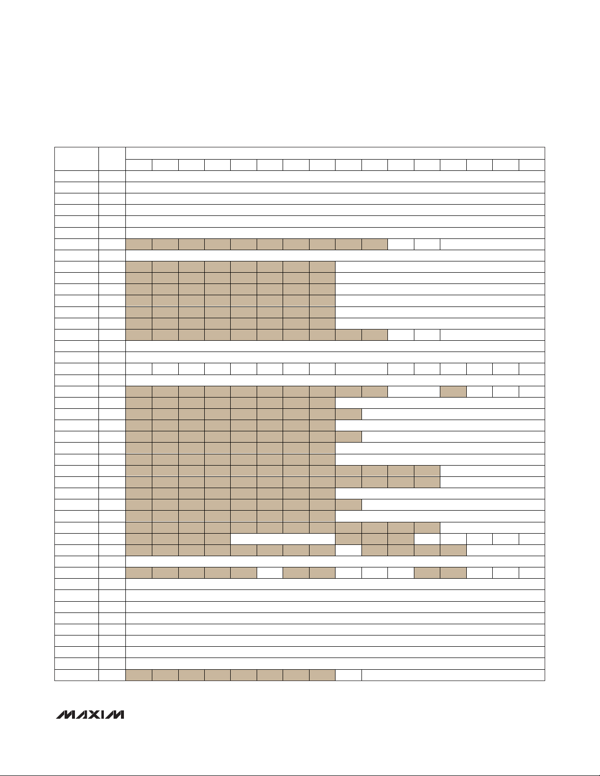
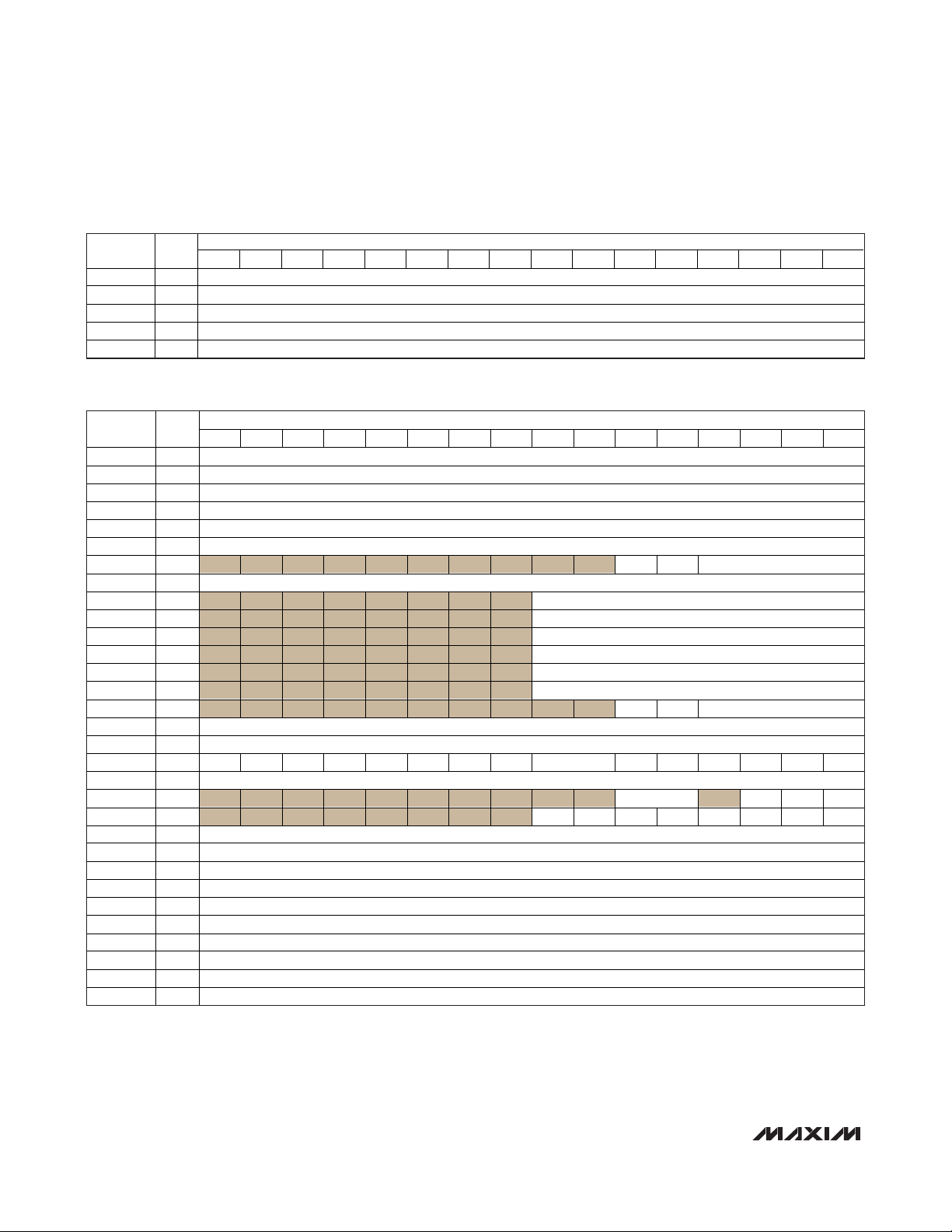
Table 1. UserCore Peripheral Registers . . . . . . . . . . . . . . . . . . . . . . . . . . . . . . . . . . . . . . . . . . . . . . . . . . . . . . . . . . .10
Table 2. UserCore Peripheral Register Default Values . . . . . . . . . . . . . . . . . . . . . . . . . . . . . . . . . . . . . . . . . . . . . . . .13
Table 3. DSPCore Peripheral Registers . . . . . . . . . . . . . . . . . . . . . . . . . . . . . . . . . . . . . . . . . . . . . . . . . . . . . . . . . . . .15
Table 4. DSPCore Peripheral Register Default Values . . . . . . . . . . . . . . . . . . . . . . . . . . . . . . . . . . . . . . . . . . . . . . . . .16
Table 5. Multipurpose Pin Description . . . . . . . . . . . . . . . . . . . . . . . . . . . . . . . . . . . . . . . . . . . . . . . . . . . . . . . . . . . . .50
Table 6. MAXQ3108 Clock Divisors . . . . . . . . . . . . . . . . . . . . . . . . . . . . . . . . . . . . . . . . . . . . . . . . . . . . . . . . . . . . . . .53
LIST OF FIGURES
LIST OF TABLES
Dual-Core Interfaces . . . . . . . . . . . . . . . . . . . . . . . . . . . . . . . . . . . . . . . . . . . . . . . . . . . . . . . . . . . . . . . . . . . . . . . .59
DSP Code Memory . . . . . . . . . . . . . . . . . . . . . . . . . . . . . . . . . . . . . . . . . . . . . . . . . . . . . . . . . . . . . . . . . . . . . .60
Intercore Communications . . . . . . . . . . . . . . . . . . . . . . . . . . . . . . . . . . . . . . . . . . . . . . . . . . . . . . . . . . . . . . . .60
Timer 2 . . . . . . . . . . . . . . . . . . . . . . . . . . . . . . . . . . . . . . . . . . . . . . . . . . . . . . . . . . . . . . . . . . . . . . . . . . . . . . . . . . .61
Timer B . . . . . . . . . . . . . . . . . . . . . . . . . . . . . . . . . . . . . . . . . . . . . . . . . . . . . . . . . . . . . . . . . . . . . . . . . . . . . . . . . .61
Timer B Use-Case Scenarios . . . . . . . . . . . . . . . . . . . . . . . . . . . . . . . . . . . . . . . . . . . . . . . . . . . . . . . . . . . . . .62
Multiply-Accumulate Unit . . . . . . . . . . . . . . . . . . . . . . . . . . . . . . . . . . . . . . . . . . . . . . . . . . . . . . . . . . . . . . . . . . . .62
Real-Time Clock . . . . . . . . . . . . . . . . . . . . . . . . . . . . . . . . . . . . . . . . . . . . . . . . . . . . . . . . . . . . . . . . . . . . . . . . . . .62
Programmable Pulse Generators . . . . . . . . . . . . . . . . . . . . . . . . . . . . . . . . . . . . . . . . . . . . . . . . . . . . . . . . . . . . . .62
In-Application Flash Programming . . . . . . . . . . . . . . . . . . . . . . . . . . . . . . . . . . . . . . . . . . . . . . . . . . . . . . . . . . . . . . . .63
Development and Technical Support . . . . . . . . . . . . . . . . . . . . . . . . . . . . . . . . . . . . . . . . . . . . . . . . . . . . . . . . . . . . .63
Additional Documentation . . . . . . . . . . . . . . . . . . . . . . . . . . . . . . . . . . . . . . . . . . . . . . . . . . . . . . . . . . . . . . . . . . . . . .63
Pin Configuration . . . . . . . . . . . . . . . . . . . . . . . . . . . . . . . . . . . . . . . . . . . . . . . . . . . . . . . . . . . . . . . . . . . . . . . . . . . . .64
Package Information . . . . . . . . . . . . . . . . . . . . . . . . . . . . . . . . . . . . . . . . . . . . . . . . . . . . . . . . . . . . . . . . . . . . . . . . . .64
TABLE OF CONTENTS (continued)
Page 4

MAXQ3108
Low-Power, Dual-Core Microcontroller
4 _______________________________________________________________________________________
RECOMMENDED DC OPERATING CONDITIONS
(VDD= V
RST
to 3.6V, TA= -40°C to +85°C.) (Notes 1, 2)
Stresses beyond those listed under “Absolute Maximum Ratings” may cause permanent damage to the device. These are stress ratings only, and functional
operation of the device at these or any other conditions beyond those indicated in the operational sections of the specifications is not implied. Exposure to
absolute maximum rating conditions for extended periods may affect device reliability.
Voltage Range on Any Pin
except V
DD
with Respect to VSS...........................-0.3V to V
DD
Voltage Range on VDDwith Respect to VSS.........-0.3V to +3.6V
Operating Temperature Range ...........................-40°C to +85°C
Storage Temperature Range .............................-65°C to +150°C
Soldering Temperature...........................Refer to the IPC/JEDEC
J-STD-020 Specification.
ABSOLUTE MAXIMUM RATINGS
PARAMETER SYMBOL CONDITIONS MIN TYP MAX UNITS
Supply Voltage VDD V
Power-Fail Reset Voltage V
1.8V Internal Regulator V
1.8V Power-Fail Reset Voltage V
Battery Supply Voltage V
Battery Current (Note 3) I
Monitors VDD 1.875 1.975 V
RST
1.71 1.8 1.89 V
REG18
Monitors REGOUT 1.62 1.71 V
REGRST
1.8 3.6 V
BAT
VDD = 0, V
BAT
RTC enabled
BAT1
VDD = 0, V
BAT
RTC enabled
Active Currentwith 32.768kHz
Crystal Connected to CX1, CX2;
FLL Selected (10MHz Output);
ENDSP = 0; All Decimators and
Sinc F ilters Off (Note 4)
I
I
I
I
DD_FLL10
/1 mode, VDD = 2.0V 1.3 2.2
DD_FLL1
/1 mode, VDD = 3.6V 1.5 2.5
DD_FLL2
PMM2 (32kHz), VDD = 2.0V 0.5 0.8
DD_FLL9
PMM2 (32kHz), VDD = 3.6V 0.6 1.0
Active Current with 32.768kHz
Crystal Connected to CX1, CX2;
I
DD_FLL14
VDD = 2.0V 1.0 1.7
FLL Selected (10MHz Output);
UserCore = /256 PMM; DSPCore
= /1 ; ENDSP = 1; Manchester
I
DD_FLL15
VDD = 3.6V 1.8 3.0
Decoders On; Decimators On
I
STOP_1
Stop-Mode Current (Note 5)
I
STOP_2
Input Low (CX1) V
Input Low (All Other Pins) V
Input High (CX1) V
Input High (All Other Pins) V
Input Hystere si s (Schm itt) V
IL1
IL2
IH1
IH2
IHYS
BOD = 1, REGEN = 0, SVMSTOP = 0, RTC
off (lowe st current stop mode)
BOD = 0, REGEN = 0, SVMSTOP = 0, RTC
off (adds brownout-reset detection)
VSS 0.20 x VDD V
VSS 0.30 x VDD V
0.75 x VDD VDD V
0.70 x VDD VDD V
0.18 V
Output Low (All Port Pins) VOL IOL = 4mA (Note 6) VSS 0.4 V
Output High (All Port Pins) VOH IOH = -4mA (Note 6) VDD - 0.4 V
3.6 V
RST
= 3.6V, 32kHz oscillator and
= 2V, 32kHz oscillator and
0.8
0.6
0.1 2.4
30 125
μA
mA
mA
μA
Page 5

MAXQ3108
Low-Power, Dual-Core Microcontroller
_______________________________________________________________________________________ 5
RECOMMENDED DC OPERATING CONDITIONS (continued)
(VDD= V
RST
to 3.6V, TA= -40°C to +85°C.) (Notes 1, 2)
Note 1: Results based on simulation data. Characterization data will be available at a later date. All voltages are referenced to
ground. Specifications to T
A
= -40°C are guaranteed by design and are not production tested.
Note 2: Typical values are not guaranteed. These values are measured at room temperature, V
DD
= 3.3V.
Note 3: This current is from V
BAT
only if (VDD< V
BAT
and VDD< V
RST
) or (STOP = 1, REGEN = 0, BOD = 1). Otherwise, this current
is from V
DD
.
Note 4: Measured on the V
DD
pin and the device not in reset. All inputs are connected to VSSor VDD. Outputs do not source/sink
any current. Timer enabled, RTC enabled, part executing JUMP $ from flash.
Note 5: If the RTC is on for parameters ISTOP_2, ISTOP_3, and ISTOP_4, a current equal to I
BAT1
is added to IDD.
Note 6: The maximum total current, I
OH(MAX)
and I
OL(MAX)
, for all outputs combined should not exceed 35mA to satisfy the maxi-
mum specified voltage drop.
Note 7: The timing listed above is clocked by 63 cycles of the internal 1MHz ±5% clock. There will be ROM code overhead, which is
a function of system clock. For data sheet purposes, a better way is to specify the limits that include ROM code execution
with specified system clock speed.
Input/Output Pin Capacitance CIO Guaranteed by design 15 pF
Input Low Current Al l Pins IIL VIN = 0.4V -30 μA
Input-Leakage Current IL Internal pullup di sabled -100 +100 nA
Input Pullup Resistor (All Inputs) RPU 60 k
CLOCK SOURCE
FLL Output Frequency f
FLL Output Accuracy f
FLASH M EMORY
System Clock During Flash
Programm ing/Era se
Flash Erase Time
Flash Programming Time Per
Word
Write/Erase C ycles 1000 Cycles
Data Retention TA = +25°C 100 Years
SUPPLY VOLTAGE MONITOR
Set Point SVTR 2.0 3.5 V
Increment Resolution 0.1 V
Default Set Point 2.7 V
Current Consumption I
Start Time t
Setup Time (Change Set Point) t
Setup Time (Stop Mode Exit) t
REAL-TIME CLOCK
RTC Input Frequency f
RTC Operating Current I
PARAMETER SYMBOL CONDITIONS MIN TYP MAX UNITS
CX1 = 32.768kHz 9.5 10.0 10.5 MHz
FLL
CX1 = 32.768kHz 1.5 ±5 %
FLL
2 MHz
Mas s erase 22.8 24 25.2
Page erase 22.8 24 25.2
(Note 7) 59.5 66.5 μs
10 μA
SVM
200 μs
SVMST
SVM_SU1
SVM_SU2
32KIN
RTC
Changing from one set point to another set
point
Exit from stop mode 8 μs
32kHz watch cr ystal 32,768 Hz
VDD = 2.0V 0.6
VDD = 3.6V 0.8
2 μs
ms
μA
Page 6
MAXQ3108
Low-Power, Dual-Core Microcontroller
6 _______________________________________________________________________________________
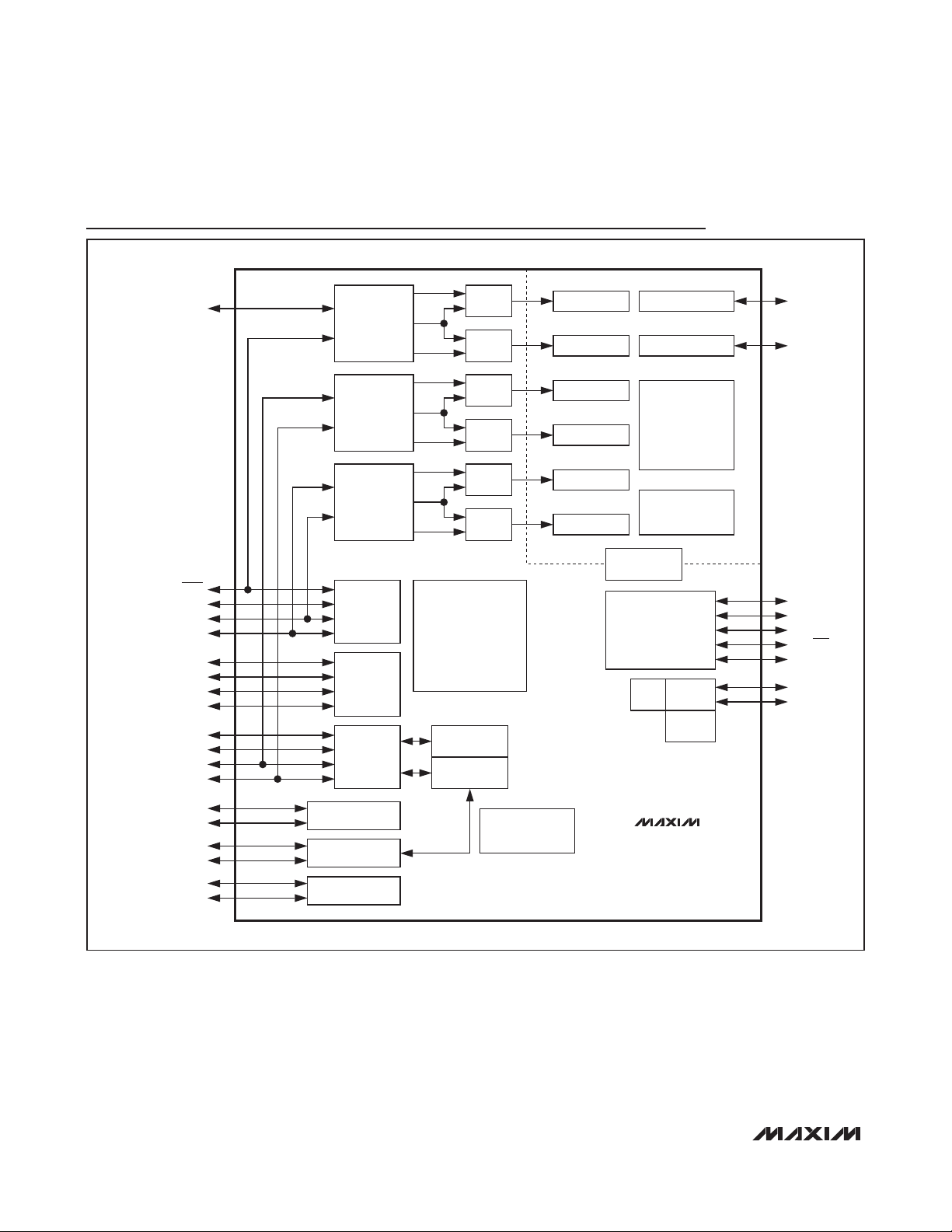
Block Diagram
I
P2.4/MDIN0P
P2.3/MDIN0N/SSEL
P2.2/SCLK/CLKO
P2.1/MDIN2N/MISO
P2.0/MDIN2P/MOSI
P1.0/TMS
P1.1/TCK
P1.2/TDI
P1.3/TDO/SQW
P1.5/TBA
P1.4/TBB
P0.3/MDIN1P/T2PB
P0.2/MDIN1N/T2P
MANCHESTER
DECODER
MANCHESTER
DECODER
MANCHESTER
DECODER
SPI
JTAG
GPIO
0
CLK
V
I
1
CLK
V
I
2
CLK
V
ADMINISTRATIVE CORE
32kW FLASH (CODE)
SINC3
FILTER
SINC3
0
FILTER
SINC3
FILTER
SINC3
1
FILTER
SINC3
FILTER
SINC3
2
FILTER
MAXQ20
2kW ROM (CODE)
1kW SRAM (DATA)
TIMER B
TIMER 2
24-BIT RESULT PULSE GENERATOR P2.5/CF1
24-BIT RESULT
24-BIT RESULT
24-BIT RESULT
24-BIT RESULT
24-BIT RESULT
MAILBOX
COMM
1.8V CORE LDO
SUPPLY MONITOR
PULSE GENERATOR P2.6/CF2
MAXQ20
DSPCORE
4kW SRAM (CODE)
512W SRAM (DATA)
MULTIPLY-
ACCUMULATE
UNIT
V
DD
GND
REGOUT
P1.6/RST
V
BAT
CX1
CX2
FLL
AND
32kHz
OSC
RTC
P1.5/TBA
P1.4/TBB
P0.7/RXD1
P0.6/TXD1
P0.1/RXD0
P0.0/TXD0
I2C MASTER
USART
USART
MULTIPLY-
ACCUMULATE
UNIT
MAXQ3108
Page 7

MAXQ3108
Low-Power, Dual-Core Microcontroller
_______________________________________________________________________________________ 7
Pin Description
PIN NAME FUNCTION
POWER PINS
21 V
17 GND Ground
20 REGOUT
19 V
15, 16 CX1, CX2
2–7, 23, 22 P0.0–P0.7
10, 11, 12,
13, 14, 18, 24P1.0–P1.6
DD
BAT
Supply Voltage. Must be bypassed with a 4.7μF capacitor with ESR < 5 and a 0.1μF ceramic
capacitor.
Regulator Output. 1.8V output. Must be connected to a 1μF low-ESR (< 1) externa l ceramic chip
capacitor.
Battery Input for Backing Up the RTC
CLOCK PINS
RTC Crystal Inputs. The RTC requires a 32.768kHz crystal to be connected in order to supply the
time base for the RTC. The 6pF load capacitors are included in the circuitry.
I/O PINS
Port 0. Port 0 functions a s both an 8-bit I/O port and as a special function interface to the I2C
master and serial UARTs 0 and 1. All pins support external interrupt functionality. The default
reset condit ion of the pins is weakl y pulled up (input). To drive output, either the port direction
register must be programmed to enable output or the alternate function module must be
configured to drive the pins. This port is acce ss ible to the UserCore onl y.
PIN PORT ALTERNATE FUNCTION
2 P0.0 TXD0/INT0
3 P0.1 RXD0/INT1
4 P0.2 MDIN1N/T2P/INT2
5 P0.3 MDIN1P/T2PB/INT3
6 P0.4 SDA/INT4
7 P0.5 SCL/INT5
23 P0.6 TXD1/INT6
22 P0.7 RXD1/INT7
Port 1. Port 1 function s a s both a 6-bit I/O port and as a special function interface to the JTAG
compatible test access port (TAP), the RTC square-wave output, and as the input/output to and
from timer B. All pins support external interrupt functionality. The default reset condition of pins
P1.0–P1.3 is the JTAG functions. To use the 4-bit port as standard GPIO, the TAP must be
disabled by user code. This port is accessible to the UserCore only.
Active-Low Reset (RST). The RST pin recognizes external active-low reset inputs and employs
an internal pullup resistor to allow for a combination of wired-OR external reset sources. An RC is
not required for power-up, as this function is provided internally. The RST pin function is enabled
on power-on reset. It i s critical that this pin not be held low externally after a power-on reset or the
device cannot exit the reset state.
PIN PORT ALTERNATE FUNCTION
10 P1.0 TMS/INT8
11 P1.1 TCK/INT9
12 P1.2 TDI/INT10
13 P1.3 TDO/SQW/INT11
14 P1.4 TBB
18 P1.5 TBA
24 P1.6 RST
Page 8

MAXQ3108
Low-Power, Dual-Core Microcontroller
8 _______________________________________________________________________________________
Detailed Description
The MAXQ3108 microcontroller is an integrated, lowcost solution to simplify the design of electricity metering and industrial control products. Standard features
include two highly optimized, single-cycle, MAXQ 16-bit
RISC microcontroller cores; 64KB of flash memory,
11KB RAM, and independent hardware stacks; general-purpose registers; and data pointers for each core.
Application-specific peripherals include hardware SPI
and I2C masters, real-time clock, programmable pulse
generators, dual UARTs (one of which that supports IR
carrier frequency modulation), and math accelerators.
At the heart of the MAXQ3108 are two MAXQ20 16-bit
RISC microcontrollers. The dual-core approach allows
one core (DSPCore) to be entirely dedicated to collection and processing of AFE samples for the metering
function, while the second core handles any communication and user-specific administrative functions. The
MAXQ3108 DSPCore operates at 10.027MHz with the
default crystal and almost all instructions execute in a
single clock cycle (100ns), while the UserCore runs at
half that frequency (5.014MHz).
The dual-core strategy promotes flexibility by allowing
the update of metering routines and parameters separately in DSPCore code and data memory. Furthermore,
an independent DSPCore solely responsible for accurate metering introduces a measure of safety and reliability since all administrative/communication functions
and interruptions are handled by the UserCore. Both
cores feature standard MAXQ power-saving system
clock-divide modes and independently implement lowpower stop (UserCore) and idle (DSPCore) modes. The
DSPCore implements an idle mode that allows CPU
execution to be halted while awaiting an ADC sample.
The UserCore implements an ultra-low-power stop
mode that automatically disables the DSPCore and
results in a quiescent current consumption of less than
1.5μA. The combination of high performance and corespecific low-power mode implementation provides
increased power efficiency and capability over competitive microcontrollers.
Microprocessor
The MAXQ20 is a low-power implementation of the new
16-bit MAXQ family of RISC cores. The core supports
the Harvard memory architecture with separate 16-bit
program and data address buses, but also provides
pseudo-Von Neumann support through utility ROM
functions. A fixed 16-bit instruction is standard, but
data can be arranged in 8 or 16 bits. The MAXQ20 core
is implemented as a nonpipelined processor with single
clock-cycle instruction execution. The data path is
implemented around register modules, and each register module contributes specific functions to the core.
The accumulator module consists of sixteen 16-bit registers and is tightly coupled to the arithmetic logic unit
(ALU). Program flow is supported by a dedicated 16level-deep hardware stack.
Execution of instructions is triggered by data transfer
between functional register modules, or between a
functional register module and memory. Since data
Pin Description (continued)
PIN NAME FUNCTION
Port 2. Port 2 functions a s both a 7-bit I/O port and as a special function interface to the CF pulse
generator outputs, clock output, and the Manchester ENDEC or SPI. The default reset condition of
the pins is weakly pulled up (input), with exception of P2.5 and P2.6, which are always outputs
and default to strong high. To drive output, either the port direction register must be programmed
to enable output, or the a lternate function module mu st be configured to drive the pins. P2.5 and
P2.6 are accessible to the DSPCore only.
1, 28, 27, 26,
25, 8, 9
P2.0–P2.6
PIN PORT ALTERNATE FUNCTION
1 P2.0 MDIN2P/MOSI
28 P2.1 MDIN2N/MISO
27 P2.2 SCLK/CLKO
26 P2.3 MDIN0N/SSEL
25 P2.4 MDIN0P
8 P2.5 CF1
9 P2.6 CF2
Page 9
MAXQ3108
Low-Power, Dual-Core Microcontroller
_______________________________________________________________________________________ 9
movement involves only source and destination modules, circuit switching activities are limited to active
modules only. For power-conscious applications, this
approach localizes power dissipation and minimizes
switching noise. The modular architecture also provides
maximum flexibility and reusability, which are important
for a microprocessor used in embedded applications.
The MAXQ instruction set is designed to be highly
orthogonal. All arithmetical and logical operations can
use any register along with the accumulator. Data movement is supported from any register to any other register. Memory is accessed through specific data pointer
registers with auto increment/decrement support.
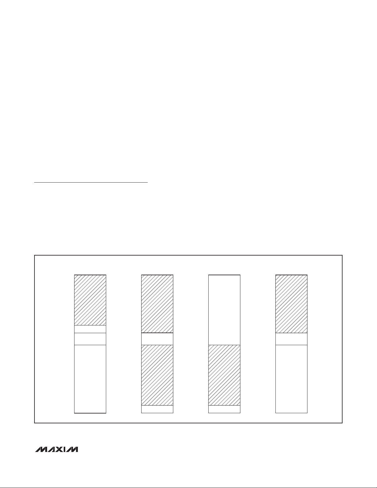
Memory
The MAXQ3108 supports a pseudo-Von Neumann
memory structure that can merge program and data into
a linear memory map. This is accomplished by mapping
the data memory into the program space or mapping
the program memory segment into the data space.
Memory access is under the control of the memory management unit (MMU). During flash programming, the
MMU maps the flash memory into data space, and the
built-in firmware provides necessary controls to the
embedded flash memory for all read/erase/write operations when the ROM loader is invoked. Additionally,
when the DSPCore is disabled, all its code SRAM (8KB)
is mapped into the data SRAM space of the UserCore.
This allows streamlined reconfiguration of the DSP code
memory or a larger data SRAM for applications not
employing DSPCore operation.
The MAXQ3108 incorporates the following:
• 4KB utility ROM
• 64KB program flash
• 2KB SRAM data memory
• 8KB program SRAM (DSPCore)
• 1KB SRAM data memory (DSPCore)
The MMU operates automatically and maps data mem-
ory as a function of the contents of the instruction pointer; that is, the execution location controls the structure
of the data memory map. The only constraint is that no
memory region is available as data when code is being
fetched from that region. For example, when executing
from flash, flash cannot be read as data. But changing
the execution location to the utility ROM through a subroutine call allows the flash memory to be read as data.
Figure 1. Memory Map
0xA800
0xA000
0x8000
0x0000
UTILITY ROM
CODE
RAM 0.5kW
2kW
FLASH
32kW
WHEN EXECUTING FROM FLASH
0xA000
0x8000
0x0800
0x0000
DATA
UTILITY ROM
2kW
RAM 0.5kW
WHEN EXECUTING FROM UTILITY ROM
0x8000
0x0800
0x0000
DATA
FLASH
32kW
RAM 0.5kW
WHEN EXECUTING FROM RAM
0xA000
0x8000
0x0000
DATA
UTILITY ROM
2kW
FLASH
32kW
Page 10

MAXQ3108
Low-Power, Dual-Core Microcontroller
10 ______________________________________________________________________________________
DSP Program RAM
A 4K Word (8KB) section of memory is available to the
DSPCore as code memory. When the DSPCore is disabled (as it is immediately following a reset event) that
block of memory appears in the UserCore data memory
map at location 0x1000. Thus, a typical startup
sequence to operate both cores might include:
1) Low-level initialization of the UserCore.
2) Copy DSP code from program flash to DSPCore
code RAM at 0x1000.
3) Enable DSPCore.
4) Poll mailbox registers to verify that DSPCore is correctly running.
For more information, see the
Dual-Core Interfaces
section.
Registers
The MAXQ family of microcontrollers uses a bank of
registers to access memory and peripherals and to perform basic CPU activities. These registers are organized into as many as 16 register modules, each of
which can have as many as 32 registers, giving a system maximum of 512 registers. The registers are divided into two sections: system registers (modules 7 to 15)
and peripheral registers (modules 0 to 5).
Since the MAXQ3108 contains two MAXQ core processors, each has a set of system registers and a set of
peripheral registers.
System Registers
The MAXQ3108 UserCore implements the standard set
of system registers as described in the
MAXQ Family
User’s Guide
. The exceptions are listed below:
• In the IMR register, bit IM5 is not implemented since
there is no module 5 implemented in the MAXQ3108.
• In the SC register, bits CDA1 and UPM are not implemented since the size of the memory in the device
does not require their implementation.
• In the IIR register, bit II5 is not implemented since
there is no module 5 implemented in the MAXQ3108.
• In the CKCN register, bits XT/RC, RGSL, and
RGMD are not implemented. Instead, bits 5 and 6
are FLLMD and FLLSL, respectively. These bits
support the frequency-locked loop (FLL) that forms
a core part of the MAXQ3108 clocking scheme.
More information is given in the
Clock
section.
The MAXQ3108 DSPCore system register complement
is identical to that found in the UserCore, with these
exceptions:
• In the IMR register, only IM0 is implemented.
• The system control (SC) register is not implemented.
• In the IIR register, only the II0 bit is implemented.
• The WDCN register is not implemented because
there is no watchdog timer in the DSPCore.
Watchdog functionality can be implemented in the
UserCore by determining if the DSPCore is responding to messages.
• In the CKCN register, the STOP, RGSL, and SWB bits
are not implemented because the corresponding
functions do not exist in the DSPCore. The FLLMD
and FLLSL bits are not implemented because a common clock block is shared with the UserCore, and
the control bits here would be redundant.
Peripheral Registers—UserCore
The MAXQ3108 UserCore exposes its peripheral complement in five modules numbered 0 to 4. Table 1
describes the functions associated with the peripheral
registers, and Table 2 shows the default values of these
registers.
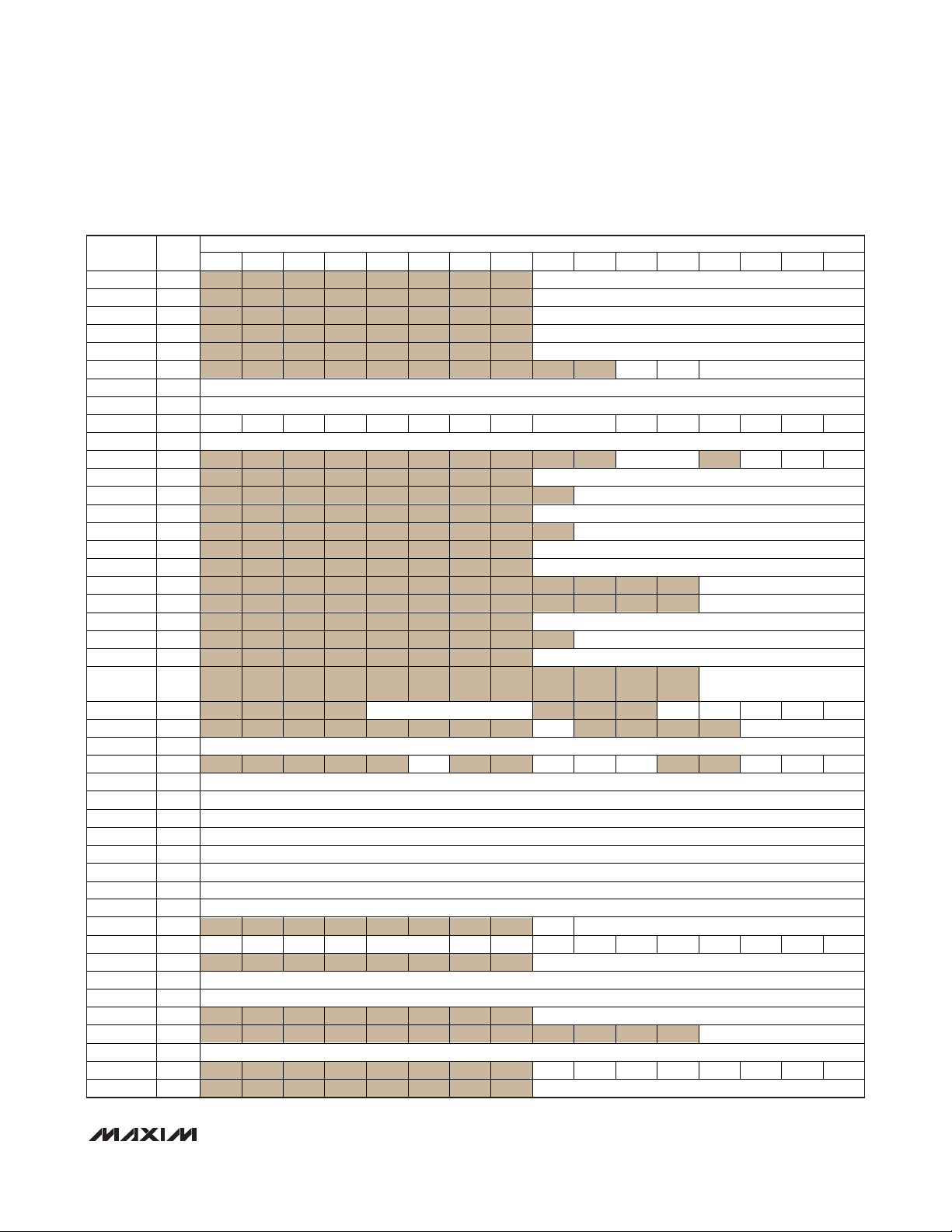
Table 1. UserCore Peripheral Registers
REGISTER
AD0 0:0 ADC0 Output Register
AD1 0:1 ADC1 Output Register
AD2 0:2 ADC2 Output Register
AD3 0:3 ADC3 Output Register
AD4 0:4 ADC4 Output Register
AD5 0:5 ADC5 Output Register
SRSP0 0:6 RSPSDV REQE RSPST
SRSP1 0:7 Slave Resp onse Register 1
AD0LSB 0:8 ADC0 Output Register LSB
MOD:
REG
15 14 13 12 11 10 9 8 7 6 5 4 3 2 1 0
BIT
Page 11
MAXQ3108
Low-Power, Dual-Core Microcontroller
______________________________________________________________________________________ 11
Table 1. UserCore Peripheral Registers (continued)
REGISTER
AD1LSB 0:9 ADC1 Output Register LSB
AD2LSB 0:10 ADC2 Output Register LSB
AD3LSB 0:11 ADC3 Output Register LSB
AD4LSB 0:12 ADC4 Output Register LSB
AD5LSB 0:13 ADC5 Output Register LSB
MREQ0 0:14 REQCDV RSPIE REQCM
MREQ1 0:15 Mast er Request Regi ster 1
MREQ2 0:16 Mast er Request Regi ster 2
ADCN 0:17 IFCS EL IF54E IF 32E IF10E MDCKS MD2E MD1E MD0E OSR ABF5 ABF4 ABF3 ABF2 ABF1 ABF0
ADCC 0:18 ADC Clock Correction Regi ster
MSTC 0:19 CCSL MD2 SNC MD1SNC MD0SNC
PO0 1:0 Port 0 Output Register
PO1 1:1 Port 1 Output Register
PI0 1:2 Port 0 Input Register
PI1 1:3 Port 1 Input Register
EIF0 1:4 Port 0 Interrupt Flag Register
EIE0 1:5 Port 0 Interrupt Enable Register
EIF1 1:6 Port 1 Interrupt Flag Regi ster
EIE1 1:7 Port 1 Interrupt Enable Regis ter
PD0 1:8 Port 0 Direction Register
PD1 1:9 Port 1 Direction Reg ister
EIES0 1:10 Port 0 External Interrupt Edge Select
EIES1 1:11
SVM 1:12 SVTH SVMSTOP SVMI SVMIE SVMRDY SVMEN
FCNTL 1:13 FBUSY FC
FDATA 1:14 Fla sh Data Register
PWCN 1:15 ENDSP BOD REGEN RSTD ECLKO FLOCK FLLEN
BB0 1:16 Battery-Backed General-Purpose Storage 0
BB1 1:17 Battery-Backed General-Purpose Storage 1
BB2 1:18 Battery-Backed General-Purpose Storage 2
BB3 1:19 Battery-Backed General-Purpose Storage 3
BB4 1:20 Battery-Backed General-Purpose Storage 4
BB5 1:21 Battery-Backed General-Purpose Storage 5
BB6 1:22 Battery-Backed General-Purpose Storage 6
BB7 1:23 Battery-Backed General-Purpose Storage 7
RTRM 1:24 TSGN TRM
RCNT 1:25 WE X32D 32KRD Y 32KBYP 32KMD FT SQE ALSF ALDF RDYE RDY BUSY ASE ADE RTCE
RTSS 1:26 RTC Subsecond Counter
RTSH 1:27 RTC Seconds Register MSW
RTSL 1:28 RTC Seconds Register LSW
RSSA 1:29 RTC Subsecond Alarm
RASH 1:30 RTC Seconds A larm MSW
RASL 1:31 RTS Seconds Alarm LSW
T2CNA 2:0 ET2 T2OE0 T2POL0 TR2L TR2 CPRL2 SS2 G2EN
T2H 2:1 Timer 2 MSB
MOD:
REG
15 14 13 12 11 10 9 8 7 6 5 4 3 2 1 0
BIT
Port 1 External Interrupt Edge
Select
Page 12
MAXQ3108
Low-Power, Dual-Core Microcontroller
12 ______________________________________________________________________________________
Table 1. UserCore Peripheral Registers (continued)
REGISTER
T2RH 2:2 Timer 2 MSB Re load Value
T2CH 2:3 Timer 2 MS B Capture/Compare Value
PO2 2:4 Port 2 Output Register
PI2 2:5 Port 2 Input Register
SCON0 2:6
SBUF0 2:7 Serial D ata Bu ffer 0
SMD0 2:8 EPWM OFS ESI SMOD FEDE
PR0 2:9 Phase Regi ster 0
PD2 2:10 Port 2 Direction Reg ister
T2CNB 2:11 ET2L T2OE1 T2POL1 TF2 TF2 L TCC2 TC2L
T2V 2:12 Timer 2 Value Register
T2R 2:13 Timer 2 Reload Register
T2C 2:14 Timer 2 C apture/Compare Regist er
T2CFG 2:15 T2CI T2DIV T2MD CCF C/T2
MCNT 3:0 OF MCW CLD SQU OPCS MSUB MMAC SUS
MA 3:1 Multiplier Operand “A” Register
MB 3:2 Multiplier Operand “B” Register
MC2 3:3 Multiplier Accumulator Register 2 (MSB, bits 47-32)
MC1 3:4 Multiplier Accumulator Regi ster 1 (bit s 31-16)
MC0 3:5 Mult ipl ier Accumulator Register 0 (LSB, bits 15-0)
SPIB 3:7 SPI Data Buffer
MC1R 3:8 Mult iplier Read Regi ster 1 (MSB, bits 31-16)
MC0R 3:9 Mult ipl ier Read Regi ster 0 (LSB, bits 15-0)
SPICN 3:13 STBY SPIC ROVR WCOL MODF MODFE MSTM SPIEN
SPICF 3:14 ESPII CHR CKPHA CKPOL
SPICK 3:15 SPI Clock Register
I2CBUF 4:0 I
I2CST 4:1 I2CBUS I2CBU SY I2CS PI I2CSCL I2CROI I2CGCI
I2CIE 4:2 I2C SPIE I2CR OIE I2CGCIE I2CNACKIE I2CALIE
TB0R 4:4 Timer B Capture/Reload Value
TB0C 4:5 Timer B C ompare Va lue
SCON1 4:6
SBUF1 4:7 Serial D ata Bu ffer 1
SMD1 4:8 ESI SMOD FEDE
PR1 4:9 Phase Regi ster 1
TB0CN 4:10 C/TB T BC S TBC R TB PS T FB E XFB T BOE DCE N EXENB TR B E TB
TB0V 4: 11 Timer B Value Regi ster
I2CCN 4:12 I2CR ST I2CSTREN I2CGCEN I2CSTO P I2CSTART I2CACK I2CSTRS I2CMODE I2CMST I2CEN
I2CCK 4:13 I2C Clock High Period I2C Clock Low Period
I2CTO 4:14 I
I2CSLA 4:15 I
MOD:
REG
15 14 13 12 11 10 9 8 7 6 5 4 3 2 1 0
BIT
SM0/
SM1 SM2 REN TB8 RB8 TI RI
FE
2
C Data Buff er Register
I2CNACK
I2CALI I2 CAMI I2CTOI I2CSTRI I2CRXI I2CTX I I2CSRI
I2CAMI
I2CTO IE I2CSTRIE I2CR XIE I2 CTXIE I2 CSRIE
SM0/
SM1 SM2 REN TB8 RB8 TI RI
FE
2
C Timeout Period
2
C Slave Address
CP/
RLB
Page 13
MAXQ3108
Low-Power, Dual-Core Microcontroller
______________________________________________________________________________________ 13
Table 2. UserCore Peripheral Register Default Values
REGISTER
AD0 0:0 0xFFFF
AD1 0:1 0xFFFF
AD2 0:2 0xFFFF
AD3 0:3 0xFFFF
AD4 0:4 0xFFFF
AD5 0:5 0xFFFF
SRSP0 0:6 0 0 0x0
SRSP1 0:7 0x0000
AD0LSB 0:8 0xFF
AD1LSB 0:9 0xFF
AD2LSB 0:10 0xFF
AD3LSB 0:11 0xFF
AD4LSB 0:12 0xFF
AD5LSB 0:13 0xFF
MREQ0 0:14 0 0 0x0
MREQ1 0:15 0x0000
MREQ2 0:16 0x0000
ADCN 0:17 0 0 0 0 0 0 0 0 0x0 0 0 0 0 0 0
ADCC 0:18 0x0000
MSTC 0:19 0x3 0 0 0
PO0 1:0 0xFF
PO1 1:1 0x7F
PI0 1:2 0xXX
PI1 1:3 0xXX
EIF0 1:4 0x00
EIE0 1:5 0x00
EIF1 1:6 0x0
EIE1 1:7 0x0
PD0 1:8 0x00
PD1 1:9 0x00
EIES0 1:10 0x00
EIES1 1:11 0x0
SVM 1:12 0x7 0 0 0 0 0
FCNTL 1:13 1 0x0
FDATA 1:14 0x0000
PWCN 1:15 0 0 0 0 0 0 0
BB0 1: 16 0xXXXX
BB1 1: 17 0xXXXX
BB2 1: 18 0xXXXX
BB3 1: 19 0xXXXX
BB4 1: 20 0xXXXX
BB5 1: 21 0xXXXX
BB6 1: 22 0xXXXX
BB7 1: 23 0xXXXX
RTRM 1:24 X X
MOD:
REG
15 14 13 12 11 10 9 8 7 6 5 4 3 2 1 0
BIT
Page 14
MAXQ3108
Low-Power, Dual-Core Microcontroller
14 ______________________________________________________________________________________
Table 2. UserCore Peripheral Register Default Values (continued)
REGISTER
RCNT 1:25 0 X X X 0xX 0 0 0 0 0 0 1 0 0 X
RTSS 1:26 0xXX
RTSH 1:27 0xXXXX
RTSL 1:28 0xXXXX
RSSA 1:29 0 xXXXX
RASH 1:30 0xX
RASL 1:31 0xXXXX
T2CNA 2:0 0 0 0 0 0 0 0 0
T2H 2:1 0x00
T2RH 2:2 0x00
T2CH 2:3 0x00
PO2 2:4 0x7F
PI2 2:5 0xFF
SCON0 2:6 0 0 0 0 0 0 0 0
SBUF0 2:7 0x00
SMD0 2:8 0 0 0 0 0
PR0 2:9 0x0000
PD2 2:10 0x00
T2CNB 2:11 0 0 0 0 0 0 0
T2V 2:12 0x0000
T2R 2:13 0x0000
T2C 2:14 0x0000
T2CFG 2:15 0 0x0 0 0x0 0
MCNT 3:0 0 0 0 0 0 0 0 0
MA 3:1 0x0000
MB 3:2 0x0000
MC2 3:3 0x0000
MC1 3:4 0x0000
MC0 3:5 0x0000
SPIB 3:7 0x0000
MC1R 3:8 0x0000
MC0R 3:9 0x0000
SPICN 3:13 0 0 0 0 0 0 0 0
SPICF 3:14 0 0 0 0
SPICK 3:15 0x00
I2CBUF 4:0 0x0000
I2CST 4:1 0 0 0 0 0 0 0 0 0 0 0 0 0 0
I2CIE 4:2 0 0 0 0 0 0 0 0 0 0 0
TB0R 4:4 0x0000
TB0C 4:5 0x0000
SCON1 4:6 0 0 0 0 0 0 0 0
SBUF1 4:7 0x0000
SMD1 4:8 0 0 0
PR1 4:9 0x0000
TB0CN 4:10 0 0 0 0 x0 0 0 0 0 0 0 0 0
MOD:
REG
15 14 13 12 11 10 9 8 7 6 5 4 3 2 1 0
BIT
Page 15
MAXQ3108
Low-Power, Dual-Core Microcontroller
______________________________________________________________________________________ 15
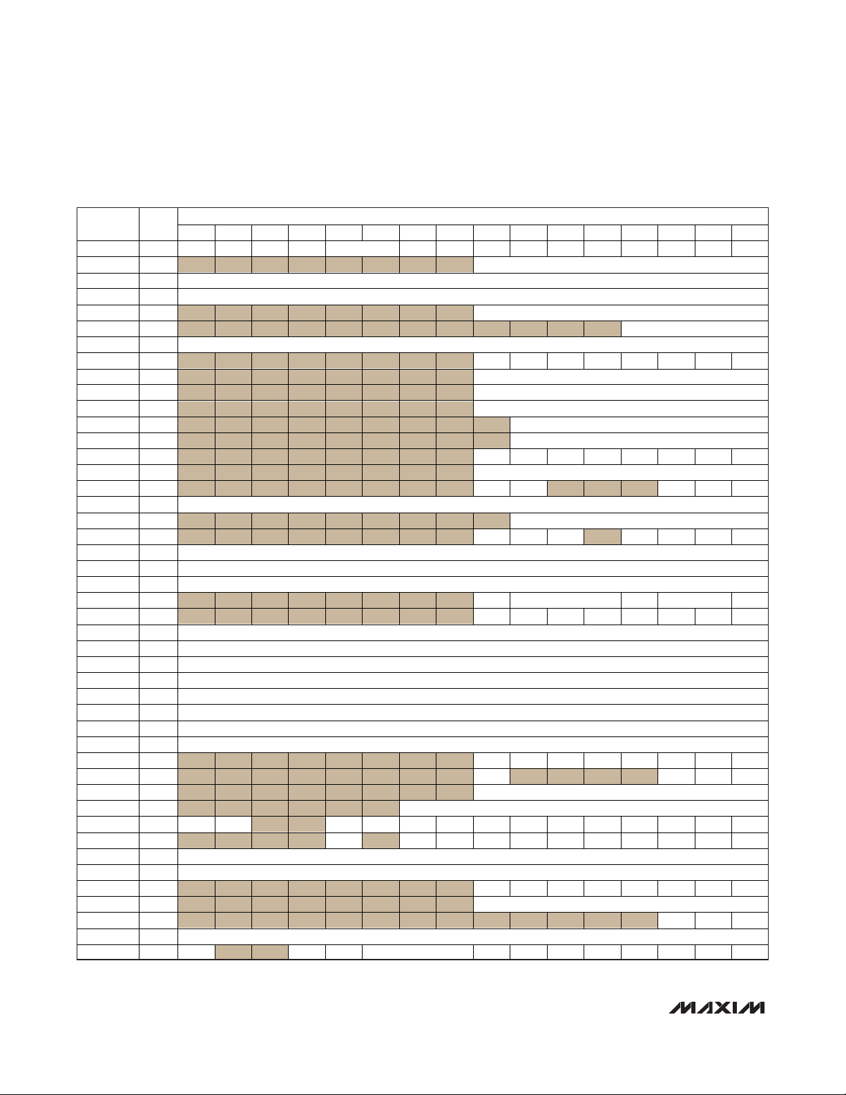
Peripheral Registers—DSPCore
The MAXQ3108 DSPCore exposes its peripheral complement in modules numbered 0 and 1. Table 3
describes the functions associated with the peripheral
registers, and Table 4 shows the default values of these
registers.
Table 2. UserCore Peripheral Register Default Values (continued)
Table 3. DSPCore Peripheral Registers
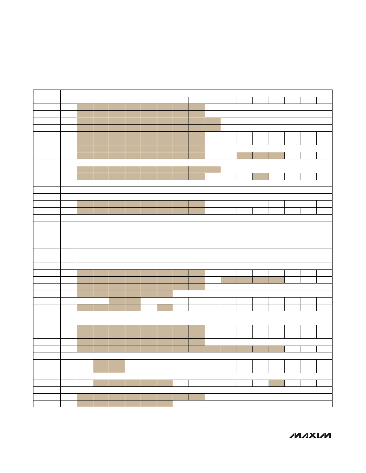
REGISTER
TB0V 4:11 0x0000
I2CCN 4:12 0 0 0 0 0 0 0 0 0 0
I2CCK 4:13 0x02 0x04
I2CTO 4:14 0x00
I2CSLA 4:15 0x000
MOD:
REG
15 14 13 12 11 10 9 8 7 6 5 4 3 2 1 0
REGISTER
AD0 0:0 ADC0 Output Reg ister
AD1 0:1 ADC1 Output Reg ister
AD2 0:2 ADC2 Output Reg ister
AD3 0:3 ADC3 Output Reg ister
AD4 0:4 ADC4 Output Reg ister
AD5 0:5 ADC5 Output Reg ister
SRSP0 0:6 RSPS DV REQE RSPST
SRSP1 0:7 Slave Response Regi ster 1
AD0LSB 0:8 ADC0 Output Register LSB
AD1LSB 0:9 ADC1 Output Register LSB
AD2LSB 0:10 ADC2 Output Register LSB
AD3LSB 0:11 ADC3 Output Register LSB
AD4LSB 0:12 ADC4 Output Register LSB
AD5LSB 0:13 ADC5 Output Register LSB
MREQ0 0:14 REQCDV RSPIE REQCM
MREQ1 0:15 Master Request Register 1
MREQ2 0:16 Master Request Register 2
ADCN 0:17 IFCSEL IF45E IF23E IF10E MDCKS MD2E MD1E MD0E OSRI ABF5 ABF4 ABF3 ABF2 ABF1 ABF0
ADCC 0:18 ADC C lock Correction Register
MSTC 0:19 CCSL MD2S NC MD1S NC MD0SN C
MCNT 1:0 OF MCW CLD SQU OPCS MSUB MMAC SUS
MA 1:1 Multipl ier Operand “A” Register
MB 1:2 Multipl ier Operand “B” Register
MC2 1:3 Multiplier Accumulator Register 2 (MSB, bits 47-32)
MC1 1:4 Multipl ier Accumulator R egister 1 (bits 31-16)
MC0 1:5 Multiplier Accumulat or Regi ster 0 (LSB, bits 15-0)
MOD:
REG
15 14 13 12 11 10 9 8 7 6 5 4 3 2 1 0
BIT
BIT
Page 16
MAXQ3108
Low-Power, Dual-Core Microcontroller
16 ______________________________________________________________________________________
Table 3. DSPCore Peripheral Registers (continued)
Table 4. DSPCore Peripheral Register Default Values
REGISTER
PO2 1:7 Port 2 Output Reg ister
MC1R 1:8 Mult iplier Read Regi ster 1 (MSB, bits 31-16)
MC0R 1:9 Mult iplier Read Register 0 (LSB, bits 15-0)
CF1D 1:12 CF1 Delay Register
CF2D 1:13 CF2 Delay Register
REGISTER
AD0 0:0 0xFFFF
AD1 0:1 0xFFFF
AD2 0:2 0xFFFF
AD3 0:3 0xFFFF
AD4 0:4 0xFFFF
AD5 0:5 0xFFFF
SRSP0 0:6 0 0 0x0
SRSP1 0:7 0x0000
AD0LSB 0:8 0xFF
AD1LSB 0:9 0xFF
AD2LSB 0:10 0xFF
AD3LSB 0:11 0xFF
AD4LSB 0:12 0xFF
AD5LSB 0:13 0xFF
MREQ0 0:14 0 0 0x0
MREQ1 0:15 0x0000
MREQ2 0:16 0x0000
ADCN 0:17 0 0 0 0 0 0 0 0 0x0 0 0 0 0 0 0
ADCC 0:18 0x0000
MSTC 0:19 0x3 0 0 0
MCNT 1:0 0 0 0 0 0 0 0 0
MA 1:1 0x0000
MB 1:2 0x0000
MC2 1:3 0x0000
MC1 1:4 0x0000
MC0 1:5 0x0000
PO2 1:7 0x0000
MC1R 1:8 0x0000
MC0R 1:9 0x0000
CF1D 1:12 0x0000
CF2D 1:13 0x0000
MOD:
REG
MOD:
REG
15 14 13 12 11 10 9 8 7 6 5 4 3 2 1 0
15 14 13 12 11 10 9 8 7 6 5 4 3 2 1 0
BIT
BIT
Page 17

MAXQ3108
Low-Power, Dual-Core Microcontroller
______________________________________________________________________________________ 17
Special Function Register Bit Descriptions
REGISTER DESCRIPTION
AD0 (00h, 00h) Analog-to-Digital Converter 0 Output Register
Initialization: This register is reset to 0xFFFF on all forms of reset.
Read/Write Access: Unrestricted read access.
Analog-to-Digital Converter 0 Output Register. This register contains the most significant 16 bits
of the current ADC0 data sample that was acquired from the respect ive sinc3 f ilter. Reading from
AD0.[15:0]:
AD1 (01h, 00h) Analog-to-Digital Converter 1 Output Register
AD2 (02h, 00h) Analog-to-Digital Converter 2 Output Register
AD3 (03h, 00h) Analog-to-Digital Converter 3 Output Register
AD4 (04h, 00h) Analog-to-Digital Converter 4 Output Register
AD5 (05h, 00h) Analog-to-Digital Converter 5 Output Register
SRSP0 (06h, 00h) Slave Response Register 0
Initialization: Th is register is reset to 00h on all forms of reset.
Read/Write Access:
SRSP0.[3:0]: RSPST[3:0]
SRSP0.4: REQE
SRSP0.5: RSPSDV
SRSP0.[7:6]: Reserved Reserved. Reads return 0.
the ADC0 register(s) results in the ABF0 flag being cleared by hardware (when set), unless the read
operation is performed simu ltaneou sly with a write. Reading a di sabled ADC returns the data last
acquired if the associated buffer full flag is set and returns FFFFh if the flag is clear.
Unrestricted read acce ss only to the UserCore (except RSPSDV; see the bit description).
Unrestricted read/write access to the DSPCore (except RSPSDV and 3:0; see the bit descriptions).
Response Status Bits 3:0. These bits can be u sed to report acknow ledgement and status of the
current command being processed by the slave and to report slave system conditions (e.g.,
watchdog timeout) that are not related to a ma ster command. To notify the master that status is
ready to be read, the RSP0DV bit shou ld be set to 1 either by software (in the case of command
status) or, in some cases, by hardware (as for the watchdog). In cases where slave hardware sets
the status bits, these bits are not writable by slave software until the status condition has been
cleared.
When the DSPCore watchdog timer reaches FFFFh, a system interrupt from the DSPCore is signaled
by the setting of the SRSP0.5 status flag along with the SRSP0.[3:0] status code of 0000b. This
hardware condit ion for the SRSP0 register persists (prevent ing software writes of these bits by the
DSPCore) until a reset of the DSPCore is executed (UserCore may disable the DSPCore through
ENDSP = 0 to force the reset).
Request Registers Interrupt Enable. Setting this bit to 1 enables an interrupt for the master
request-command data valid (interrupt) flag (REQCDV). The master request-command data valid
flag is reported in MREQ0.5 (and the associated command code is contained in MREQ0.[3:0]).
Clearing thi s bit to 0 disable s the interrupt associated with the master request-command data va lid
flag.
Response Status Data Valid Flag. This f lag can only be set by the slave (DSPCore) or slave
hardware once a va lid status or system interrupt condition is supplied in the RSPST[3:0] field of the
SRSP0 register to notif y the master that valid status is read y for reading. Status information or data
could also be contained in SRSP1, so the slave should only set this flag when all data has been
loaded (included any that is loaded to SRSP1). This flag can onl y be cleared by the master
(UserCore) software unle ss the status condition that caused hardware to set the flag persists (e.g.,
slave watchdog counter timeout). If made ava ilable by the slaveCPU, more information can be
ascertained about the status by additional master request read commands.
Page 18
MAXQ3108
Low-Power, Dual-Core Microcontroller
18 ______________________________________________________________________________________
Special Function Register Bit Descriptions (continued)
SRSP1 (07h, 00h) Slave Response Register 1
Initialization: Th is register is reset to 0000h on all forms of reset.
Read/Write Access:
SRSP1.[15:0]:
Unrestricted read acce ss only to the UserCore.
Unrestricted read/write access to the DSPCore.
Response Register 1 Bits 15:0. The se bits are used to supply output data to the master. To notif y
the master that data is ready to be read, the RSPCDV bit should be set to 1 by software. The slave
should not write further data to SRSP1 until the va lid condition (RSPSDV = 1) is cleared by the
master software.
AD0LSB (08h, 00h) Analog-to-Digital Converter 0 Least Significant Byte Output Register
Initialization: This register i s reset to FFh on all forms of reset.
Read/Write Access: Unrestricted read access.
Analog-to-Digital Converter 0 Least Significant Byte Output Register. This register always provides
read access to the least significant byte of the most current ADC0 data sample acquired from the
respective sinc3 filter. See the below table for the least significant byte available OSR options.
Reading from the AD0 register results in the ABF0 f lag being cleared by hardware (when set)
unless the read operation is performed simultaneously with a write. What this means is that when
OSR > 32, AD0LSB should be read first if the clearing of ABF0 is intended to indicate that the full
AD0LSB.[7:0]:
AD1LSB (09h, 00h) Analog-to-Digital Converter 1 Least Significant Byte Output Register
AD2LSB (0Ah, 00h) Analog-to-Digital Converter 2 Least Significant Byte Output Register
AD3LSB (0Bh, 00h) Analog-to-Digital Converter 3 Least Significant Byte Output Register
AD4LSB (0Ch, 00h) Analog-to-Digital Converter 4 Least Significant Byte Output Register
AD5LSB (0Dh, 00h) Analog-to-Digital Converter 5 Least Significant Byte Output Register
result (AD0LSB and AD0) was read. Reading a disabled ADC returns the data la st acquired if the
assoc iated buffer full flag is set and returns FFFFh if the flag is clear.
OSR ADC DATA OUTPUT WIDTH AD0LSB FORMAT
32 16 00000000b
64 19 d2–d0, 00000b
128 22 d5–d0, 00b
256 24 d7–d0
MREQ0 (0Eh, 00h) Master Request Register 0
Initialization: Th is register is reset to 00h on all forms of reset.
Read/Write Access:
MREQ0.[3:0]: REQCM[3:0]
MREQ0.4: RSP1E
MREQ0.5: REQCDV
MREQ0.[7:6]: Reserved Reserved. Reads return 0.
Unrestricted read/write access to the UserCore (except REQCDV; see the bit description).
Unrestricted read acce ss only to the DSPCore (except REQCDV; see the bit description).
Request Command Bits 3:0. These bits are written by the master to supply a command request to the
sla ve. To notify the slave that a command is ready to be read, the REQ0DV bit should be set to 1.
Response Registers Interrupt Enable. Setting this bit to 1 enables an interrupt for the slave
response status data valid flag (which is a ss ociated with Response Registers 0 and 1). The status
data va lid (interrupt) flag is reported in SRSP0.5. Clearing this bit to 0 disables the interrupt
assoc iated with the respon se status data valid flag.
Request Command Data Valid Flag. This f lag can only be set by the master (UserCore). This flag
should be set once a valid command is supplied in the REQCM[3:0] field of the MREQ0 and/or data
supplied in the MREQ1, MREQ2 registers to notif y the s lave that the se registers are ready for
reading. This flag can only be cleared by slave (DSPCore) software.
Page 19

MAXQ3108
Low-Power, Dual-Core Microcontroller
______________________________________________________________________________________ 19
Special Function Register Bit Descriptions (continued)
MREQ1 (0Fh, 00h) Master Request Register 1
Initialization: This register is reset to 0000h on all forms of reset.
Read/Write Access:
MREQ1.[15:0]:
MREQ2 (10h, 00h) Master Request Register 2
Initialization: This register is reset to 0000h on all forms of reset.
Read/Write Access:
MREQ2.[15:0]:
ADCN (11h, 00h) Analog-to-Digital Converter Control Register
Initialization: This register is cleared to 0000h on all forms of reset.
Read/Write Access:
ADCN.0: ABF0
ADCN.1: ABF1
ADCN:2: ABF2
ADCN.3: ABF3
ADCN.4: ABF4
Unrestricted read/write access only to the UserCore.
Unrestricted read acce ss only to the DSPCore.
Master Request Register 1 Bits 15:0. These bit s are used to supply follow-on address and data
information for commands issued by the master. To notify the slave that data i s read y to be read,
the REQCDV bit should be set to 1. The master should poll the REQCDV bit to know when the slave
has read MREQ1 and when it is safe to write further data to MREQ1.
Unrestricted read/write access only to the UserCore.
Unrestricted read acce ss only to the DSPCore.
Master Request Register 2 Bits 15:0. These bit s are used to supply follow-on address and data
information for commands issued by the master. To notify the slave that data i s read y to be read,
the REQCDV bit should be set to 1. The master should poll the REQCDV bit to know when the slave
has read MREQ2 and when it is safe to write further data to MREQ2.
UserCore: Unrestricted read/write access except bits 0:5 are read only and 6:7 have hardware
restricted write access.
DSPCore: Read-only.
ADC0 Buffer Full Flag. This bit is set by hardware to indicate that a sample is available from
ADC0. An interrupt request i s generated to a CPU if IF01E = 1 and interrupts are not otherwise
masked globally or modularly. This bit is cleared by hardware by a CPU read (either the UserCore
or the DSPCore) of the AD0 output register. The A BF0 and ABF1 flags are set in the same clock
cycle.
ADC1 Buffer Full Flag. This bit is set by hardware to indicate that a sample is available from
ADC1. An interrupt request i s generated to a CPU if IF01E = 1 and interrupts are not otherwise
masked globally or modularly. This bit is cleared by hardware by a CPU read (either the UserCore
or the DSPCore) of the AD1 output register. The A BF0 and ABF1 flags are set in the same clock
cycle.
ADC2 Buffer Full Flag. This bit is set by hardware to indicate that a sample is available from
ADC2. An interrupt request i s generated to a CPU if IF23E = 1 and interrupts are not otherwise
masked globally or modularly. This bit is cleared by hardware by a CPU read (either the UserCore
or the DSPCore) of the AD2 output register. The A BF2 and ABF3 flags are set in the same clock
cycle.
ADC3 Buffer Full Flag. This bit is set by hardware to indicate that a sample is available from
ADC3. An interrupt request i s generated to a CPU if IF23E = 1 and interrupts are not otherwise
masked globally or modularly. This bit is cleared by hardware by a CPU read (either the UserCore
or the DSPCore) of the AD3 output register. The A BF2 and ABF3 flags are set in the same clock
cycle.
ADC4 Buffer Full Flag. This bit is set by hardware to indicate that a sample is available from
ADC4. An interrupt request i s generated to a CPU if IF45E = 1 and interrupts are not otherwise
masked globally or modularly. This bit is cleared by hardware by a CPU read (either the UserCore
or the DSPCore) of the AD4 output register. The A BF4 and ABF5 flags are set in the same clock
cycle.
Page 20

MAXQ3108
Low-Power, Dual-Core Microcontroller
20 ______________________________________________________________________________________
Special Function Register Bit Descriptions (continued)
ADC5 Buffer Full Flag. This bit is set by hardware to indicate that a sample is available from
ADC5. An interrupt request i s generated to a CPU if IF45E = 1 and interrupts are not otherwise
ADCN:5: ABF5
ADCN.[7:6]: OSR[1:0]
ADCN.8: MD0E
ADCN.9: MD1E
ADCN.10: MD2E
ADCN.11: MDCKS
ADCN.12: IF10E
masked globally or modularly. This bit is cleared by hardware by a CPU read (either the UserCore
or the DSPCore) of the AD5 output register. The A BF4 and ABF5 flags are set in the same clock
cycle.
Oversampling Rate Bits 1:0. These register bits control the oversampling rate applied by all of the
cubic sinc digital fi lter s (as given in the table below). These bits are writable on ly when all
Manchester decoders are disabled.
OSR[1:0] OVERSAMPLING RATE
00b 32
01b 64
10b 128
11b 256
Manchester Decoder 0 Enable. Thi s bit controls whether Manchester decoder 0 and the two
assoc iated cubic sinc filters are enabled or disabled. When MD0E i s conf igured to logic 1,
Manchester decoder 0 and the assoc iated cubic sinc f ilters are enabled. Thi s is a special case
where enabling the special function input (Manchester decoder input) forces a specific input mode
(single-ended or differentia l) based upon the PO bit for the port pin corresponding to the Manchester
decoder positive input (e.g., PO2.4 controls the single-ended or differential configuration for
Manchester decoder 0 when MD0E = 1). When the PO bit = 0, single-ended mode is in effect. When
PO bit = 1, differential mode is in effect. When MD0E is configured to logic 0, these hardware
blocks are disabled. This bit is write acce ssible on ly to the UserCore.
Manchester Decoder 1 Enable. Thi s bit controls whether Manchester decoder 1 and the two
assoc iated cubic sinc filters are enabled or disabled. When MD1E i s conf igured to logic 1,
Manchester decoder 1 and the assoc iated cubic sinc f ilters are enabled. Thi s is a special case
where enabling the special function input (Manchester decoder input) forces a specific input mode
(single-ended or differentia l) based upon the PO bit for the port pin corresponding to the Manchester
decoder positive input (e.g., PO0.3 controls the single-ended or differential configuration for
Manchester decoder 1 when MD1E = 1). When the PO bit = 0, single-ended mode is in effect. When
PO bit = 1, differential mode is in effect. When MD1E is configured to logic 0, these hardware
blocks are disabled. This bit is write acce ssible on ly to the UserCore.
Manchester Decoder 2 Enable. Thi s bit controls whether Manchester decoder 2 and the two
assoc iated cubic sinc filters are enabled or disabled. When MD2E i s conf igured to logic 1,
Manchester decoder 2 and the assoc iated cubic sinc f ilters are enabled. Thi s is a special case
where enabling the special function input (Manchester decoder input) forces a specific input mode
(single-ended or differentia l) based upon the PO bit for the port pin corresponding to the Manchester
decoder positive input (e.g., PO2.0 controls the single-ended or differential configuration for
Manchester decoder 2 when MD2E = 1). When the PO bit = 0, single-ended mode is in effect. When
PO bit = 1, differential mode is in effect. When MD2E is configured to logic 0, these hardware
blocks are disabled. This bit is write acce ssible on ly to the UserCore.
Manchester Decoders Clock Speed Select. This bit must be configured to tell the Manchester
decoders whether a fast or slow bit-stream sampling clock is used. When configured to 0, the
decoders e xpect that the sampling clock is faster than the clock source being used b y the AD02
modulator(s). When configured to 1, the decoders expect that the sampling clock is s lower that
than being used by the AD02.
ADC Interrupt Flags 1 and 0 Enable. This bit serves a s the loca l interrupt enable for the ADC cubic
sinc filter output buffers 1 and 0.
Page 21

MAXQ3108
Low-Power, Dual-Core Microcontroller
______________________________________________________________________________________ 21
Special Function Register Bit Descriptions (continued)
ADCN.13: IF32E
ADCN.14: IF54E
ADCN.15: IFCSEL
ADCC (12h, 00h) Analog-to-Digital Clock Correction Register
Initialization: This register i s reset to 0000h.
Read/Write Access: Unrestricted read access.
ADCC.[15:0]:
MSTC (13h, 00h) Manchester Decoder Status Register
Initialization: This register i s reset to 30h.
Read/Write Access: Unrestricted read access. Unrestricted write acces s to bits 5:4 (see description).
MSTC.0: MD0SNC
MSTC.1: MD1SNC
MSTC.2: MD2SNC
MSTC.3: Reserved Reserved. Reads return 0.
ADC Interrupt Flags 3 and 2 Enable. This bit serves a s the loca l interrupt enable for the ADC cubic
sinc filter output buffers 3 and 2.
ADC Interrupt Flags 5 and 4 Enable. This bit serves a s the loca l interrupt enable for the ADC cubic
sinc filter output buffers 5 and 4.
ADC Interrupt Flag Core Select. This bit controls the routing and the ability to clear the ADC
interrupt flags. When this bit is configured to 0, the ADC interrupt capability and the ability to clear
the associated flags belongs to the UserCore. When this bit is configured to 1, only the DSPCore
can be interrupted and has the ability to clear the interrupt flags. This bit is write accessible only to
the UserCore.
ADC Clock Correction Value 15:0. This value reflect s the count (measurement) of decoder sync
bits during the predefined duration of 32 kHz x 2
The clock correction facilit y is enabled on any write to the CCSL[1:0] bits (other than the 11b
disable request). The ADCC register reads 0000h to indicate a bus y (measu ring) condition unti l the
measurement completes, at which point, the ADCC register is updated.
Manchester Decoder 0 Synchronization Status Bit. This bit reflects the synchronization status of
Manchester decoder 0. When the decoder has achieved synchronizat ion, thi s bit i s set to 1. When
the decoder cannot or ha s not yet detected the required alternating synchronization bit in the
Manchester bit stream, this bit is cleared to 0. Once synchronized, lo ss of synchronization is
signaled ( i.e., b it i s c leared) once three sync bit errors are detected in 10 frames. If fewer than three
errors are detected in 10 frames, the synchronization bit error counter restarts on the next sync bit
error.
Manchester Decoder 1 Synchronization Status Bit. This bit reflects the synchronization status of
Manchester decoder 1. When the decoder has achieved synchronizat ion, thi s bit i s set to 1. When
the decoder cannot or ha s not yet detected the required alternating synchronization bit in the
Manchester bit stream, this bit is cleared to 0. Once synchronized, lo ss of synchronization is
signaled ( i.e., b it i s c leared) once three sync bit errors are detected in 10 frames. If fewer than three
errors are detected in 10 frames, the synchronization bit error counter restarts on the next sync bit
error.
Manchester Decoder 2 Synchronization Status Bit. This bit reflects the synchronization status of
Manchester decoder 2. When the decoder has achieved synchronizat ion, thi s bit i s set to 1. When
the decoder cannot or ha s not yet detected the required alternating synchronization bit in the
Manchester bit stream, this bit is cleared to 0.
9
clocks for the decoder selected by CCSL[1:0].
Page 22

MAXQ3108
Low-Power, Dual-Core Microcontroller
22 ______________________________________________________________________________________
Special Function Register Bit Descriptions (continued)
Clock Correction Hardware Selection Bits 1:0. These bits are used to enable and assign the
clock measurement hardware to one of the three Manche ster decoders. When these bits are 11b,
the clock measurement utility is disabled. Writing these bits to any other state enables one clock
measurement interval. When the clock measurement interval is enabled, the ADCC output register
is cleared to 0000h to indicate a busy (mea suring) condition. No hardware protection is in place to
prevent attempts to measure a disabled decoder, which wou ld result in see ing a persistent busy
(ADCC = 0000h) condition. The table below summarizes the measurement options.
Separate phys ical implementations of these two control bits exist for the U serCore and the
MSTC.[5:4]: CCSL[1:0]
MSTC.[7:6]: Reserved Reserved. Reads return 0.
DSPCore. The ENDSP bit controls which bits are used to control the cloc k correction measurement
hardware. When ENDSP = 0, the UserCore CCSL[1:0] bits control the hardware. When ENDSP = 1,
the DSPCore CCSL[1:0] bits control the hardware. The bits not being used b y the hardware are still
write acce ssible but have no effect on the hardware. Once a cloc k measurement is requested, a
second request should not be issued from the other core. There is no need for hardware protection
again st th is pos sib il ity; the ADCC register can be polled to ascertain the busy status.
CCLS[1:0]
00b Decoder 0
01b Decoder 1
10b Decoder 2
11b Disabled
CLOCK MEASUREMENT (SYNC BIT
FREQUENCY)
PO0 (00h, 01h) Port 0 Output Register (8-Bit Register)
Initialization: This register is set to 0FFh on all forms of reset.
Read/Write Access: Unrestricted read/write.
Port 0 Output Register Bits 7:0. The PO0 register stores output data for port 0 when it is defined as
an output port and controls whether the internal weak p-channel pullup transistor is
PO0.[7:0]:
PO1 (01h, 01h) Port 1 Output Register (8-Bit Register)
Initialization: This register is set to 07Fh on all forms of reset.
Read/Write Access: Unrestricted read/write.
PO1.[6:0]:
PO1.7: Reserved Reserved. Reads return 0.
enabled/disabled if a port pin is defined as an input. The contents of this register can be modified
by a write access. Reading from the register returns the contents of the register. Changing the
direction of port 0 does not change the data contents of the register.
Port 1 Output Register Bits 6:0. The PO1 register stores output data for port 1 when it is defined as
an output port and controls whether the internal weak p-channel pullup transistor is
enabled/disabled if a port pin is defined as an input. The contents of this register can be modified
by a write access. Reading from the register returns the contents of the register. Changing the
direction of port 1 does not change the data contents of the register.
Special note about P1.6: The RST input function remains enabled on P1.6 unless it is explicitly
disabled (RSTD = 1). This mean s that the ports control bits (PD, PO) can be used to generate a
reset (e.g., by driving the p in low).
Page 23

MAXQ3108
Low-Power, Dual-Core Microcontroller
______________________________________________________________________________________ 23
Special Function Register Bit Descriptions (continued)
PI0 (02h, 01h) Port 0 Input Register
Initialization: The reset value for this reg ister is dependent on the logical states of the p ins.
Read/Write Access: Unrestricted read-only.
Port 0 Input Register Bits 7:0. The PI0 register always reflects the logic state of its pins when read.
PI0.[7:0]:
PI1 (03h, 01h) Port 1 Input Register
Initialization: The reset va lue for thi s register is 0s ss sss sb, where “ s” depends on the logica l state of the pin.
Read/Write Access: Unrestricted read.
PI1.[6:0]:
PI1.7: Reserved Reserved. Read returns 0.
EIF0 (04h, 01h) External Interrupt Flag 0 Register
Initialization: EIF0 is cleared to 00h on all forms of reset.
Read/Write Access: Unrestricted read/write.
EIF0.[7:0]: IE[7:0]
Note that each port pin has a weak pullup circuit when functioning as an input and the p-channel
pullup transistor is controlled by its respective PO bits. If the PO bit is set to 1, the weak pullup is
on, if the PO bit is cleared to 0, the weak pullup is off and forces the port pin into three-state.
Port 1 Input Register Bits 6:0. The PI1 register always reflects the logic state of its pins when read.
Note that each port pin has a weak pullup circuit when functioning as an input and the p-channel
pullup transistor is controlled by its respective PO bits. If the PO bit is set to 1, the weak pullup is
on, if the PO bit is cleared to 0, the weak pullup is off and forces the port pin into three-state.
Interrupt Edge Detect Bits 7:0. These bits are set when a negative edge (ITx = 1) or a positive
edge (ITx = 0) is detected on the interrupt x pin. Setting any of the bits to 1 generate s an interrupt to
the CPU if the corresponding interrupt is enabled. This bit remains set until cleared by software or a
reset. It mu st be cleared by software before ex iting the interrupt source routine or another interrupt
is g enerated as long as the b it remains set.
EIE0 (05h, 01h) External Interrupt Enable 0 Register
Initialization: EIE0 is cleared to 00h on all forms of reset.
Read/Write Access: Unrestricted read/write.
EIE0.[7:0]: EX[7:0]
EIF1 (06h, 01h) External Interrupt Flag 1 Register
Initialization: EIF1 is cleared to 00h on all forms of reset.
Read/Write Access: Unrestricted read/write.
EIF1.[3:0]: IE[11:8]
EIF1.[7:4]: Re served Reserved. Reads return 0.
Enable External Interrupt Bits 7:0. Setting any of these bits to 1 enables the corresponding
external interrupt. Clearing any of the bits to 0 disables the corresponding interrupt function.
Interrupt Edge Detect Bits 11:8. These bits are set when a negative edge (ITx = 1) or a pos iti ve
edge (ITx = 0) is detected on the interrupt x pin. Setting any of the bits to 1 generate s an interrupt to
the CPU if the corresponding interrupt is enabled. This bit remains set until cleared by software or a
reset. It mu st be cleared by software before ex iting the interrupt source routine or another interrupt
is g enerated as long as the b it remains set.
Page 24

MAXQ3108
Low-Power, Dual-Core Microcontroller
24 ______________________________________________________________________________________
Special Function Register Bit Descriptions (continued)
EIE1 (07h, 01h) External Interrupt Enable 1 Register
Initialization: EIE1 is cleared to 00h on all forms of reset.
Read/Write Access: Unrestricted read/write.
EIE1.[3:0]: EX[11:8]
EIE1.[7:4]: Reserved Reserved. Reads return 0.
PD0 (08h, 01h) Port 0 Direction Register
Initialization: This register is cleared to 00h on all forms of reset.
Read/Write Access: Unrestricted read/write.
PD0.[7:0]:
PD1 (09h, 01h) Port 1 Direction Register
Initialization: This register is cleared to 00h on all forms of reset.
Read/Write Access: Unrestricted read/write.
PD1.[6:0]:
PD1.7: Reserved Reserved. Reads return 0.
Enable External Interrupt Bits 11:8. Setting any of these bits to 1 enables the corresponding
external interrupt. Clearing any of the bits to 0 disables the corresponding interrupt function.
Port 0 Direction Register Bits 7:0. PD0 is used to determine the direction of the Port 0 function. The
port pins are independently controlled by their direction bits. When a bit is set to 1, its corresponding
pin is used as an output; data in the PO register is driven on the p in. When a bit is cleared to 0, its
corresponding pin is used as an input, and allows an external signal to drive the pin. Note that each
port pin has a weak pul lup circuit when functioning as an input and the p-channel pullup transistor is
controlled by its respective PO bits. If the PO bit is set to 1, the weak pullup is on; if the PO bit is
cleared to 0, the weak pullup i s off and forces the port pin into three-state.
Port 1 Direction Register Bits 6:0. PD1 is used to determine the direction of the port 1 function.
The port pins are independently controlled by their direction bit. When a bit is set to 1, its
corresponding pin i s u sed as an output; data in the PO register is driven on the pin. When a bit is
cleared to 0, its corresponding pin is used as an input, and allows an external signal to drive the
pin. Note that each port pin has a weak pullup circuit when functioning as an input and the pchannel pullup trans istor is controlled by its respective PO bits. If the PO bit is set to 1, the weak
pullup is on; if the PO bit is cleared to 0, the weak pullup is off and forces the port pin into threestate. Special note about P1.6: The RST input function remains enabled on P1.6 unless it is
expl icitl y disabled (RSTD = 1). Thi s means that the ports control bit s (PD, PO) can be used to
generate a reset (e.g., by driving the pin low).
EIE S0 (0Ah, 01h) External Interrupt Edge Select 0 Register
Initialization: EIES0 is cleared to 00h on all forms of reset.
Read/Write Access: Unrestricted read/write.
Edge Select for External Interrupt Bits 7:0
EIES0.[7:0]: IT[7:0]
ITx = 0: External interrupt x is positive-edge triggered.
ITx = 1: External interrupt x is negative-edge triggered.
Page 25

MAXQ3108
Low-Power, Dual-Core Microcontroller
______________________________________________________________________________________ 25
Special Function Register Bit Descriptions (continued)
EIE S1 (0Bh, 01h) External Interrupt Edge Select 1 Register
Initialization: EIES1 is cleared to 00h on all forms of reset.
Read/Write Access: Unrestricted read/write.
External Interrupt Edge Select Bits 11:8
EIES1.[3:0]: IT[11:8]
EIES1.[7:4]: Reserved Reserved. Reads return 0.
SVM (0Ch, 01h) Supply Voltage Monitor Register (16-Bit Register)
Initialization: This register is set to 0700h on all forms of reset.
Read/Write Access:
SVM.0: SVMEN
SVM.1: SVMRDY
SVM.2: SVMIE
SVM.3: SVMI
SVM.4: SVMSTOP
SVM.[7:5]: Reserved Reserved. Reads return 0.
SVM.[11:8]: SVTH[3:0]
SVM.[15:12]: Reserved Reserved. Reads return 0.
ITx = 0: External interrupt x is positive-edge triggered.
ITx = 1: External interrupt x is negative-edge triggered.
Unrestricted read/write except SVMRDY and SVMTH. The suppl y voltage monitor ready (SVMRDY)
bit i s set and cleared by hardware only. SVMTH can only be written to when the supply vo ltage
monitor is di sabled (SVMEN = 0).
Supply Voltage Monitor Enable. Setting thi s bit to 1 enables the monitoring of suppl y voltage
according to SVMTH settings. Clearing this bit to 0 disables the suppl y voltage monitor ing
circuitry.
Supply Voltage Monitor Ready. This bit is set to 1 to ind icate that the supply voltage monitor is
ready for use. This bit i s cleared to 0 when SVMEN = 0 or on entrance to stop mode if SVMSTOP = 0.
Supply Voltage Monitor Interrupt Enable. Setting this bit to 1 generates an interrupt to the CPU
when SVMI is set to 1. Clearing this bit to 0 disables the interrupt from generating.
Supply Voltage Monitor Interrupt. This bit is set to 1 when the supply voltage falls below the set
point defined by SVTH. Clearing this bit to 0 c lears the interrupt. However, if the suppl y voltage i s
still below the set point, this flag is set again. Setting this bit to 1 causes an interrupt to the CPU
when SVMIE = 1.
Supply Voltage Monitor Stop Mode Enable. Setting this bit to 1 enables the supply voltage monitor
circuit to operate during stop mode if SVMEN = 1. Clearing this bit to 0 disable s the supply voltage
monitor when stop mode is enabled.
Supply Voltage Threshold Bits [3:0]. These bits are used to se lect a user-defined supply voltage
threshold under which an interrupt is generated to the CPU if enabled. The level can be adjusted
from 2.0V to 3.5V in a 0.1V increment. The supply voltage monitor is enabled by setting SVMEN =
1. The default value is 07h (2.7V).
Supply Voltage Monitor Threshold = 2.0V + SVMTH[3:0] x 0.1V
Note that the SVTH bits can only be modified when SVMEN = 0. Writing to these bits is ignored if
SVMEN = 1.
Page 26

MAXQ3108
Low-Power, Dual-Core Microcontroller
26 ______________________________________________________________________________________
Special Function Register Bit Descriptions (continued)
FCNTL (0Dh, 01h) Flash Memory Control Register
Initialization: This register i s set to 80h on POR and is unaffected by all other forms of reset.
Unrestricted read, bits 2:0 are write access ible only by utilit y ROM or logical data memory. (This
Read/Write Access:
FCNTL.[2:0]: FC[2:0]
FCNTL.[6:3]: Re served Reserved. Reads return 0.
FCNTL.7: FBUSY
register is not accessible by program code ins ide the flash memory because of the rule governing
the pseudo-Von Neumann mapping. Access is blocked by hardware.) Also, write access to FCNTL
is prohibited when FBUSY is 0.
Flash Command Bits 2:0. The below table shows the commands for flash operations provided by
these bits. The MMU supports only these commands; other settings are reser ved. Using any
reserved command results in no operation.
FC[2:0] FLASH COMMANDS
000 Read Mode (default)
001 Verify Information Block
010 Write Informat ion Block
011 Write Main Memory B loc k
100 Erase Information Block
101 Page Erase of Main Memory Block
110 Mass Erase of Main Memory Block
111 Load Trim Information
Flash Busy. This busy flag is cleared to a logic 0 to indicate the start of an erase/program
operation by the MMU immediately following the command sequence. It is hold low until the end of
the operation. Set/reset of this f lag is synchronized with the sy stem clock.
FDATA (0Eh, 01h) Flash Memory Data Register
Initialization: This register is cleared to 0000h on all forms of reset.
Read/Write Access:
FDATA.[15:0]:
PWCN (0Fh, 01h) Power Control Register (16-Bit Register)
Initialization:
Read/Write Access: Unrestricted read. FLOCK and 32KRDY are read-only.
PWCN.0: FLLEN
PWCN.1: FLOCK
Unrestricted read, write accessible only b y ut il ity ROM or logical data memory. (This register i s not
accessible for program code inside the flash memory due to the rule governing the pseudo-Von
Neumann mapping.). Also, write access to FCNTL is prohibited when FBUSY is 0.
Thi s register is used by the user software or the ROM loader to support the f lash
erase/program/verify operation. Writing to this SFR has no effect on flash operation until a va lid
fla sh command is first entered through the FC[2:0] bits of the FCNTL SFR. All fla sh operation must
be initiated by providing a valid command in the FCNTL control register followed by writing target
address and data by the FDATA SFR (when required by the command).
Implemented register bits (except for the ECLKO and ENDSP bit) are unaffected by resets other than
power-on reset. The ECLKO and ENDSP bits are reset to 0 on any reset. On power-on reset, this
register is reset to 0000h (except that HFXD is 1 for PCK = 11b).
FLL Lock Enable. Setting this bit to 1 enables the FLL if it is not already running, and causes it to
lock to the 32K input. When this bit is cleared to 0, the FLL is disabled if it is not providing the
system clock.
FLL Locked. This is a read-only statu s bit. Th is bit is automatically reset to 0 when FLLEN is
changed from 0 to 1 and set to 1 when the FLL is locked to the 32.768kHz clock. This bit is also
reset to 0 on entry to stop mode.
Page 27

MAXQ3108
Low-Power, Dual-Core Microcontroller
______________________________________________________________________________________ 27
Special Function Register Bit Descriptions (continued)
Enable Clock Output Pin. Setting this bit to 1 enables the output of the DSPCore undivided system
PWCN.2: ECLKO
PWCN.[3:4]: Reserved Reserved. Reads return 0.
PWCN.5: RSTD
PWCN.6: REGEN
PWCN.7: BOD
PWCN.[9:8]: Reserved Reserved. Reads return 0.
PWCN.10: ENDSP
PWCN.[15:11]: Reserved Reserved. Reads return 0.
clock on P2.2. The P2.2 pin also serves as the SPI serial clock (SCLK) special function. The SPI
hardware should not be used when the CLKO output is enabled. The ECLKO bit can be used in the
hybrid configuration to al low the test sy stem clock to be routed to the DS8102 CLKIO pin.
Reset Pin Disable. When set to a logic 1, the reset input function is disconnected from the external
RST pin. The port pin can then be used for other purposes. When cleared to a logic 0, the reset
input function is connected to the external pin; however, the port directional and output controls
still apply. This bit defaults to 0 on power-on reset on ly.
Regulator Enable. When set to 1, the internal regulator remains powered on when the device is
placed in stop mode. When cleared to 0, the internal regulator is shut down to con serve power. The
regulator i s always enab led outside of stop mode, independent of the REGEN bit setting.
Brownout-Detection Disable. This bit determines whether the brownout detection is enabled in stop
mode when the regulator is off (REGEN = 0). When the regulator is enabled (as in normal operation
or when REGEN = 1 in stop mode), the brownout detection is alwa ys enabled, independent of the
BOD bit setting. Otherwise, when set to 1, the brownout reset detection for V
the device i s placed into stop mode. When placed into stop mode with BOD = 1 and REGEN = 0,
the brownout reset comparator is shut down. When configured to 0 with REGEN = 0, the brownoutdetection function is enabled for detecting the condition V
Enable DSPCore. This active-high bit is cleared to 0 on any UserCore reset and when the
UserCore invoke s stop mode. When cleared, the DSPCore is completely dis abled. This bit is
read/write accessible only to the UserCore so that it controls when the slave DSPCore is allowed to
operate. When this bit is written to 1, the DSPCore is removed from reset and is allowed to operate.
DD
< V
during stop mode.
RST
is disabled when
DD
BB0 (10h, 01h) Battery-Backed Register 0 (16-Bit Register)
Initialization:
Read/Write Access: Unrestricted read/write access.
BB0.[15:0]:
BB2 (12h, 01h)
BB3 (13h, 01h)
BB4 (14h, 01h)
BB5 (15h, 01h)
BB6 (16h, 01h)
BB7 (17h, 01h)
Thi s register is battery bac ked through POR so long as V
is indeterminate on the very first POR and mu st be configured initially by the user. This register is
unaffected by other reset s.
Battery-Backed Register 0 Bits 15:0. This register is intended for quick and convenient storage of
critical data through VDD power outages (avoiding the more time-consuming write attempts to
external serial NV memory).
See the BB0 register for description.
BAT(MIN)
< V
BAT
< V
BAT(MAX)
; however, it
Page 28

MAXQ3108
Low-Power, Dual-Core Microcontroller
28 ______________________________________________________________________________________
Special Function Register Bit Descriptions (continued)
RTRM (18h, 01h) Real-Time Clock Trim Register (8-Bit Register)
Initialization:
Read/Write Access:
RTRM.[6:0]: TRM[6:0]
RTRM.7: TSGN
RCNT (19h, 01h) Real-Time Clock Control Register (16-Bit Register)
Initialization:
Read/Write Access:
RCNT.0: RTCE
RCNT.1: ADE
RCNT.2: ASE
RCNT.3: BUSY
RCNT.4: RDY
RCNT.5: RDYE
Thi s register is battery bac ked through POR so long as V
is indeterminate on the very first POR and mu st be configured initially by the user. This register is
unaffected by other reset s.
Unrestricted read, write access only when the WE = 1 and BUSY = 0. An attempted write operation
is not complete until hardware clears the BUSY bit.
RTC Trim Calibration Register Bits 6:0. These register bits provide a binary value between 00h–
7Fh, which is used for adjusting 32K clocks insertion/removal. At every 10-second interval, the
number of 32K cloc ks equal to the RTRM[6:0] numeric va lue is in serted/removed from the RTC
counter depending on the value in the TSGN bit. The trim bit s are write protected by WE. WE must
be set to 1 for the bits to be updated.
RTC Trim Sign Bit. This register bit selects whether 32K clocks are inserted (TSGN = 0) or
removed (TSGN = 1).
This register is initialized to 0sssss000000100sb on all forms of reset. Bits 14–10 and bit 0 are
battery bac ked through POR so long as V
are indeterminate on the very f irst POR and must be configured by the user, but are unaffected by
other resets.
Unrestricted read. Bit 0 (RTCE) is write accessible on ly when WE = 1 and BUSY = 0. Bits 3 (BUSY)
and 13 (32KRDY) are read-only. B it 4 can be cleared to 0 when RTCE = 1; it can never be set to 1
by software. Bit 15 is unrestricted write. All other bits are write accessible only when BUSY = 0.
Real-Time Clock Enable. The RTCE is the real-time enable bit. Setting this bit to logic 1 activates
the clocking by allowing the divided clock to the ripple counters. Clearing this bit to logic 0
disables the clock.
Alarm Time-of-Day Enable. The ADE bit i s the RTC’s time-of-day alarm enable and mu st be set to
logic 1 for the alarm to generate a system interrupt request. When the ADE is cleared to logic 0, the
time-of-day alarm is disabled; no interrupt is generated even the alarm is set.
Alarm Subsecond Enable. The ASE bit is the RTC’s subsecond timer enable and must be set to
logic 1 for the subsecond alarm to generate a sy stem interrupt request. When the ASE is cleared to
logic 0, the subsecond alarm is disabled; no interrupt is generated even the alarm is set.
RTC Busy. This bit i s set to 1 by hardware when an y of the following conditions occur:
1) System reset.
2) Software writes to RTC count registers or trim register.
3) Software changes RTCE, ASE, or ADE.
For conditions 2) and 3), the write or change should not be con sidered complete until hardware
clears the BUSY bit. This is an indication that a 32kHz synchronized version of the register bit(s) is
in place.
RTC Ready. This bit is set to 1 by hardware when the RTC count registers update. It can be cleared
to 0 by software at an y time. It is also cleared to 0 by hardware just prior to an update of the RTC
count register. This bit can generate an interrupt if the RDYE bit is set to 1.
RTC Ready Enable. Setting this bit to 1 allows a system interrupt to be generated when RDY
becomes activ e (if interrupts are enabled globally and modularly). C learing thi s bit to 0 disable s
the RDY interrupt.
BAT(MIN)
< V
BAT
BAT(MIN)
< V
BAT(MAX)
< V
< V
BAT
BAT(MAX)
. These battery-backed bits
; however, it
Page 29

MAXQ3108
Low-Power, Dual-Core Microcontroller
______________________________________________________________________________________ 29
Special Function Register Bit Descriptions (continued)
RCNT.6: ALDF
RCNT.7: ALSF
RCNT.8: SQE
RCNT.9: FT
RCNT.[11:10]: 32KMD
RCNT.12: 32KBYP
RCNT.13: 32KRDY
RCNT.14: X32D
RCNT.15: WE
Alarm Time-of-Day Flag. This bit is set when the contents of RTSH and RTSL counter registers
match the 20-bit value in the RASH and RASL alarm registers. Setting the ALDF causes an interrupt
request to the CPU if the ADE is set and interrupt is allowed at the system level. This flag must be
cleared by software once set. Thi s alarm is qualified as a wake up to the stop and the switchback
function if its interrupt has not been masked.
Alarm Subsecond Flag. This bit i s set when the subsecond timer has been reloaded by the RSSA
register. Setting the ALSF causes an interrupt request to the CPU if the ASE is set and the interrupt is
allowed at the system level. Thi s flag must be cleared by software once set. This alarm is qualified
as a wake up to the stop and the switchback function if its interrupt have not been ma sked.
RTC Square-Wave Output Enable. Setting this bit to a logic 1 enab les either the 1Hz tap or the
512Hz tap of the RTC to the SQW pin. When cleared to 0, the SQW pin is not driven by the RTC.
Because the P1.3 pin has two possible special function outputs, the SQW special function takes
priority over the JTAG TDO specia l function output if both are enabled.
RTC Frequency Test. This register bit selects the frequency output that is poss ible on the SQW pin
if the square-wave output is enabled. Setting FT = 1 se lect s the 512Hz output (when SQE = 1) while
FT = 0 selects the 1Hz output (when SQE = 1). This bit has no function if the square-wave output is
disabled.
32K Oscillator Mode Bits [1:0]. These two bits determine the 32K oscillator operation modes as
shown in the below table. Changing the value of these bits when the 32K input is enabled (X32D =
0) resets the 32KRDY bit to 0 if the new setting requires the oscillator circuitry to warm up.
32KMD[1:0] 32K OSCILLATOR MODE
00 A lways operate in no ise immune mode.
01 A lways operate in quiet mode.
Operate in noise immune mode normally, switch to quiet mode on stop
10
11
32K Bypass Enable. Setting this bit to 1 disables the internal oscillator circuitry connected
between the internal CX1 and CX2 pin s. In this configuration, any peripheral that is us ing the 32K
input can be driven e xternally by a cloc k signa l prov ided on the CX1 pin. C learing this bit to 0
enables the internal crystal oscillator circuitry. When the internal oscillator circuitry is enabled,
250ms are required before the crystal oscillator has warmed up. This bit can only be changed
when RTCE = 0. Note that this bit has no effect when X32D is set to 1.
32K Input Ready. This bit is set to 1 by hardware after the 32K oscillator has warmed up and is
ready to source as input to system clock or peripherals. This bit is cleared to 0 when X32D is set
to 1 or when X32D = 0 and 32KMD values ha ve changed to require the 32K circuitry to warm up.
User application should check that the 32K input is ready (32KRDY = 1) before enabling any
peripherals that use the 32K input as time base; otherwise timing accuracy i s compromised. This
bit is read-only.
32K External Input Disable. Setting this bit to 1 disables the 32K circuitry. No external 32K clock
source is accepted. Clearing this bit to 0 enables the 32K circuitry. The source of the input is
configured through the 32KBYP bit. This b it can only be changed when RTCE = 0. Note: If X32D = 0
in stop mode, the 32K source is still available in stop mode.
RTC Write Enable. This register bit serves as a protection mechanism against undesirable writes
to the RTCE bit and RTRM register. Thi s bit must be set to a 1 to give write access to the RTRM
register and the RTCE bit; otherwise (when the WE bit = 0) these protected bits are read-only.
mode entr y. On stop mode exit, the CPU code execution must wait for 32K
oscillator to transition (warm up) from quiet mode to noise immune mode.
Operate in noise immune mode normally, switch to quiet mode on stop mode
entry. On stop mode exit, the CPU code execution can occur during the 32K
oscillator transition (warm up) from quiet mode to noise immune mode.
Page 30

MAXQ3108
Low-Power, Dual-Core Microcontroller
30 ______________________________________________________________________________________
Special Function Register Bit Descriptions (continued)
RTSS (1Ah, 01h) RTC Subsecond Counter Register (8-Bit Register)
Initialization:
Read/Write Access:
RTSS.[7:0]:
RTSH (1Bh, 01h) RTC Second Counter High Register (16-Bit Register)
Initialization:
Read/Write Access:
RTSH.[15:0]:
RTSL (1Ch, 01h) RTC Second Counter Low Register (16-Bit Register)
Initialization:
Read/Write Access:
RTSL.[15:0]:
Thi s register is battery bac ked through POR so long as V
is indeterminate on the very first POR and mu st be configured initially by the user. This register is
unaffected by other reset s.
Write accessible when RTCE = 0 and BUSY = 0. Read accessible at all times, but the value could
be indeterminate if RDY = 0. Software should be careful to read this register only when RDY = 1.
RTC Subsecond Counter Bit 7:0. This ripple counter represents 1/256-second resolution for the
RTC and its content is incremented with each 256Hz clock tick derived from the 32.768kHz
oscillator. When the counter rollover, its output is used to drive the 32-bit se cond counter.
Thi s register is battery bac ked through POR so long as V
is indeterminate on the very first POR and mu st be configured initially by the user. This register is
unaffected by other reset s.
Write accessible when RTCE = 0 and BUSY = 0. Read accessible at all times, but the value could
be indeterminate if RDY = 0. Software should be careful to read this register only when RDY = 1.
RTC Second Counter High Bit 15:0. This register conta ins the most significant bits for the 32-bit
second counter. The RTC is a ripple counter that consists of cascading the 32-bit second counter
and 8-bit subsecond counter (RTSH, RTSL, and RTSS).
Thi s register is battery bac ked through POR so long as V
is indeterminate on the very first POR and mu st be configured initially by the user. This register is
unaffected by other reset s.
Write accessible when RTCE = 0 and BUSY = 0. Read accessible at all times, but the value could
be indeterminate if RDY = 0. Software should be careful to read this register only when RDY = 1.
RTC Second Counter Low Bit 15:0. Th is register contain s the least s ignificant bits for the 32-bit
second counter. The RTC is a ripple counter that consists of cascading the 32-bit second counter
and 8-bit subsecond counter (RTSH, RTSL, and RTSS).
BAT(MIN)
BAT(MIN)
BAT(MIN)
< V
< V
< V
BAT
BAT
BAT
< V
< V
< V
BAT(MAX)
BAT(MAX)
BAT(MAX)
; however, it
; however, it
; however, it
RSSA (1Dh, 01h) RTC Subsecond Alarm Register (8-Bit Register)
Initialization:
Read/Write Access: Unrestricted read. Write accessible when BUSY = 0 and either (ASE = 0 or RTCE = 0).
RSSA.[7:0]:
Thi s register is battery bac ked through POR so long as V
is indeterminate on the very first POR and mu st be configured initially by the user. This register is
unaffected by other reset s.
RTC Subsecond Alarm Register Bit 7:0. This register contains the reload value for the subsecond
alarm. The ALSF bit is set when an autoreload occurs.
BAT(MIN)
< V
BAT
< V
BAT(MAX)
; however, it
Page 31

MAXQ3108
Low-Power, Dual-Core Microcontroller
______________________________________________________________________________________ 31
Special Function Register Bit Descriptions (continued)
RASH (1Eh, 01h) RTC Alarm Time-of-Day High Register (8-Bit Register)
Initialization:
Read/Write Access:
RASH.[3:0]:
RASH.[7:4]: Reserved Reserved. Reads return 0.
RASL (1Fh, 01h) RTC Alarm Time-of-Day Low Register (16-Bit Register)
Initialization:
Read/Write Access: Unrestricted read. Write accessible when BUSY = 0 and either (ADE = 0 or RTCE = 0).
RASL.[15:0]:
Thi s register is battery bac ked through POR so long as V
is indeterminate on the very first POR and mu st be configured initially by the user. This register is
unaffected by other reset s.
Bits 3:0 are write accessible when either (ADE = 0 or RTCE = 0). Bits 3:0 are read accessib le at all
times. Bit s 7:4 are not write access ible and alway s read 0.
RTC Time-of-Day High Bit 3:0. This register conta ins the most significant bits for the 24-bit time-ofday alarm. The time-of-day alarm is formed by the RASH and the RASL registers and only the lower
20 bits is meaningful for the alarm function. The time-of-day alarm is triggered when 1) the
subsecond counter rolls over and 2) the 20 significant bits of the RASH:RASL register pair match
the 20 least signif icant bits of the RTC (the RTSH:RTSL register pair).
Thi s register is battery bac ked through POR so long as V
is indeterminate on the very first POR and mu st be configured initially by the user. This register is
unaffected by other reset s.
RTC Time-of-Day Low Bit 15:0. This register contains the least significant bits for the 20-bit time-ofday alarm. The time-of-day alarm is formed by the RASH and the RASL registers and only the lower
20 bits are meaningful for the alarm function. The time-of-day alarm is triggered when 1) the
subsecond counter rolls over and 2) the 20 significant bits of the RASH:RASL register pair match
the 20 least signif icant bits of the RTC (the RTSH:RTSL register pair).
BAT(MIN)
BAT(MIN)
< V
< V
BAT
BAT
< V
< V
BAT(MAX)
BAT(MAX)
; however, it
; however, it
T2CNA (00h, 02h) Timer 2 Control Register A
Initialization: This register is cleared to 00h on all forms of reset.
Read/Write Access: Unrestricted read/write.
Gating Enable. This bit enables the external T2P pin to gate the input clock to the 16-bit (T2MD =
0) or highest 8-bit (T2MD = 1) timer. Gating uses T2P as an input, thus it can only be used when
T2OE0 = 0 and C/T2 = 0. Gating is not possible on the low 8-bit timer (T2L) when timer 2 is
operated in dual 8-bit mode. Gating does not make sense when counter operation is selected as
T2CNA.0: G2EN
the T2 input is being counted. The G2EN bit serves a different purpose when capture and reload
have been defined for both edges (CCF[1:0] = 11b and CPRL2 = 1). For this special case, setting
G2EN = 1 allows the T2POL0 bit to specify which edge does not cause a reload. If T2POL0 is 0,
there is no reload on the falling edge; if T2POL0 is 1, there i s no reload on the rising edge.
0 = gating disabled
1 = gating enabled
Page 32

MAXQ3108
Low-Power, Dual-Core Microcontroller
32 ______________________________________________________________________________________
Special Function Register Bit Descriptions (continued)
Single Shot. This bit is used to automatically override or delay the effect of the TR2 bit setting. The
single-shot bit is only useful in the timer mode of operation (C/T2 = 0) and should not be set to 1
when the counter mode of operation is enabled (C/T2 = 1).
Compare Mode: If SS2 is written to a 1 wh ile in compare mode, one cyc le of the defined waveform
(reload to o verflow) is output to the T2P, T2PB pins as prescribed by T2POL1:0 and T2OE[1:0]
controls. The only time that this does not immediately occur is when a gating condition is also
defined. If a gating condition is defined, the single-shot cycle cannot occur until the gating
condition is remo ved. If the specified nongated leve l is already in effect, the single- shot period
T2CNA.1: SS2
T2CNA.2: CPRL2
T2CNA.3: TR2
T2CNA.4: TR2L
T2CNA.5: T2POL0
starts. The gated single-shot output is not supported in dual 8-bit mode.
Capture Mode: If SS2 is written to a 1 while in capture mode, the timer is hal ted and the single-shot
capture cycle does not begin until 1) the edge specified b y CCF[1:0] i s detected or 2) the defined
gating condition is removed. Once running, the timer continue s running (as allowed by the gate
condition) until the defined capture s ingle-shot edge is detected. In this way , the SS2 bit can be
used to dela y the running of a timer until an edge is detected (setting both SS2 and TR2 = 1) or
override the TR2 = 0 bit setting for one capture cyc le (setting only SS2 = 1). When both edges are
defined for capture CCF[1:0] = 11b, the T2POL0 bit serves to define the single-shot start/end edge:
falling edge if T2POL0 = 1; rising edge if T2POL0 = 0. No interrupt flag is set when the starting
edge for the single-shot capture cycle is detected. The single-shot capture cycle always ends
when the next s ingle-shot edge i s detected. The start/end edge is defined by T2POL0. This bit is
intended to automate pulse-width measurement (low or high) and duty cyc le/period mea surement.
Capture and Reload Enable. This bit enables a reload (in addition to a capture) on the edge
specified by CCF[1:0] when operating in capture/reload mode (C/T2 = 0). If both edges are defined
for capture/reload (CCF[1:0] = 11b), enabling the gating control (G2EN = 1) allows the T2POL0 bit to
be used to prevent a reload on one of the edges. If T2POL0 is 0, no reload on the falling edge; if
T2POL[0] is 1, no reload on the rising edge.
0: capture on edge(s) specified by CCF[1:0] bits
1: capture and reload on edge(s) spec ified by CCF[1:0] bits
Timer 2 Run Enable. Thi s bit starts/stop timer 2. In the dual 8-bit mode of operation, this bit applies
only to the T2H timer/counter. Otherwise, the bit applies to the full 16-bit T2H:T2L timer/counter.
When the timer is stopped (TR2 = 0), the timer registers hold their count. The single-shot bit (SS2)
can override and/or delay the effect of the TR2 bit.
0: timer 2 stopped
1: timer 2 run
Timer 2 Low Run Enable. This bit starts/stops the low 8-bit timer (T2L) when dual 8-bit mode (T2MD
= 1) is in effect. This bit has no effect when T2MD = 0.
0: timer 2 low stopped
1: timer 2 low run
Timer 2 Polarity Select 0. When the timer 2 output function has been enabled (T2OE0 = 1), the
polarity select b it defines the starting log ic level for the T2P output waveform. When T2POL0 = 0,
the starting state for the T2P output is logic-low. When T2POL0 = 1, the starting state for the T2P
output is logic-high. The T2POL0 bit can be modified any time, but takes effect on the external pin
when T2OE0 is changed from 0 to 1. When the timer 2 pin is being u sed a s an input (T2OE0 = 0),
the polarity select bit define s wh ich logic leve l can be used to gate the timer input clock (when
CCF[1:0]<>11b). When CCF[1:0] = 11b, T2POL0 defines which edge can start/stop a single-shot
capture and which edge reload can be sk ipped (if CPRL2 = 1 and G2EN = 1).
Page 33

MAXQ3108
Low-Power, Dual-Core Microcontroller
______________________________________________________________________________________ 33
Special Function Register Bit Descriptions (continued)
Timer 2 Output Enable 0. This register bit enables the timer 2 output function for the external T2P
pin. The table below shows t imer 2 output possibi litie s for the T2, T2PB pins.
T20E[1:0] T2MD T2P PIN T2PB PIN
00 X Port latch data Port latch data
T2CNA.6: T2OE0
T2CNA.7: ET2
T2H (01h, 02h) Timer 2 Most Significant Byte
Initialization: The timer 2 most significant byte is cleared to 00h on all forms of reset.
Read/Write Access: Unrestricted read/write.
T2H.[7:0]: Timer 2 MSB Bits 7:0. This register is used to load and read the most significant 8-bit value in timer 2.
T2RH (02h, 02h) Timer 2 Most Significant Byte Reload
Initialization: The timer 2 mo st significant byte is cleared to 00h on al l forms of reset.
Read/Write Access: Unrestricted read/write.
T2RH.[7:0]:
Enable Timer 2 Interrupts. This bit serves as the local enable for timer 2 interrupt sources that fall
under the TF2 and TCC2 interrupt flags.
Timer 2 Reload MSB Bits 7:0. This register is u sed to load and read the most significant 8-bit
value in timer 2.
01 0 16-bit PWM output Port latch data
10 0 Port latch data 16-bit PWM output
11 0 16-bit PWM output 16-bit PWM output
01 1 8-bit PWM output (T2H) Port latch data
10 1 Port latch data 8-bit PWM output (T2L)
11 1 8-bit PWM output (T2H) 8-bit PWM output (T2L)
T2CH (03h, 02h) Timer 2 Most Significant Byte Capture/Compare
Initialization: This byte is cleared to 00h on all forms of reset.
Read/Write Access: Unrestricted read/write.
T2CH.[7:0]:
PO2 (04h, 02h) Port 2 Output Register (8-Bit Register)
Initialization: This register i s set to 1Fh on all forms of reset.
Read/Write Access: Unrestricted read/write.
PO2.[6:0]:
PO2.7: Reser ved Reserved. Reads return 0.
Timer 2 Capture/Compare MSB Bits 7:0. This register reflects the upper byte of the timer 2
capture/compare value and is read/write accessible at all times.
Port 2 Output Register Bits 6:0. The PO2 register stores output data for port 2 when it i s defined a s
an output port and controls whether the internal weak p-channel pullup transistor is
enabled/disabled if a port pin is defined as an input. The contents of this register can be modified
by a write access. Reading from the register returns the contents of the register. Changing the
direction of port 2 does not change the data contents of the register.
Page 34

MAXQ3108
Low-Power, Dual-Core Microcontroller
34 ______________________________________________________________________________________
Special Function Register Bit Descriptions (continued)
PI2 (05h, 02h) Port 2 Input Register
Initialization: The reset value for this reg ister is dependent on the logical states of the p ins.
Read/Write Access: Unrestricted read-only.
Port 2 Input Register Bits 6:0. The PI2 register always reflects the logic state of its pins when read.
PI2.[6:0]:
PI2.7: Reserved Reserved. Reads return 0.
SCON0 (06h, 02h) Serial Port 0 Control Register
Initialization: The serial port control is c leared to 00h on all forms of reset.
Read/Write Access: Unrestricted read/write.
SCON0.0: RI
SCON0.1: TI
SCON0.2: RB8
SCON0.3: TB8
SCON0.4: REN
SCON0.5: SM2
SCON0.6: SM1 Serial Port 0 Mode Bit 1
Note that each port pin has a weak pullup circuit when functioning as an input and the p-channel
pullup transistor is controlled by its respective PO bits. If the PO bit is set to 1, the weak pullup is
on; if the PO bit is cleared to 0, the weak pullup is off and forces the port pin into three-state.
Receive Interrupt Flag. This bit indicates that a data byte has been received in the serial port
buffer. The bit is set at the end of the 8th bit for mode 0, after the last sample of the incoming stop
bit for mode 1 subject to the value of the SM2 bit, or after the last sample of RB8 for modes 2 and
3. This bit must be cleared by software once set.
Transmit Interrupt Flag. This bit indicates that the data in the serial-port data buffer has been
completely shifted out. It is set at the end of the la st data bit for all modes of operation and mu st
be cleared by software once set.
9th Received Bit State. This bit identifies the state of the 9th b it of received data in serial port
modes 2 and 3. When SM2 is 0, it is the state of the stop bit in mode 1. This bit has no meaning in
mode 0.
9th Transmission Bit State. This bit defines the state of the 9th transmiss ion bit in serial port
modes 2 and 3.
Receive Enable
REN_0 = 0: Serial port 0 receiver disabled.
REN_0 = 1: Serial port 0 receiver enabled for modes 1, 2 and 3. Initiate synchronou s reception for
mode 0.
Serial Port Mode Bit 2. Setting this bit in mode 1 ignores reception if an invalid stop bit is
detected. Setting this bit in mode 2 or 3 enables multiprocessor communications, and prevents the
RI bit from being set and the interrupt from being asserted if the 9th bit received is 0. This bit is
also used to support mode 0 for clock selection.
SM2 = 0: clock is divided by 12
SM2 = 1: clock is divided by 4
Page 35

MAXQ3108
Low-Power, Dual-Core Microcontroller
______________________________________________________________________________________ 35
Special Function Register Bit Descriptions (continued)
Serial Port 0 Mode Bit 0/Framing Error Flag. When FEDE is 0, this is the SM0 bit. When FEDE is
set to 1, this bit is the FE that is set upon detection of an invalid stop bit. It must be cleared by
software. Modification of th is bit when FEDE is set has no effect on the serial mode.
MODE SM2 SM1 SM0 FUNCTION
0 0 0 0 Synchronous 8 12 system clock
0 1 0 0 Synchronous 8 4 system clock
SCON0.7:SM0/FE
SBUF0 (07h, 02h) Serial Data Buffer 0
Initialization: This buffer is cleared to 00h on all forms of reset.
Read/Write Access: Unrestricted read/write.
SBUF0.[7:0]:
1 X 1 0 A synchronous 10
2 0 0 1 Asynchronou s 11
2 1 0 1 Asynchronou s (MP) 11
3 0 1 1 Asynchronou s 11
3 1 1 1 Asynchronou s (MP) 11
Serial Data Buffer 0 Bit 7:0. Data for serial port 0 is read from or written to this location. The serial
transm it and recei ve buffers are separate, but both are addressed at this location.
LENGTH
(BITS)
PERIOD
64/16 baud cloc k
(SMOD = 0/1)
64/32 system clock
(SMOD = 0/1)
64/32 system clock
(SMOD = 0/1)
64/16 baud cloc k
(SMOD = 0/1)
64/16 baud cloc k
(SMOD = 0/1)
SMD0 (08h, 02h) Serial Port Mode Register 0
Initialization: This register is cleared to 00h on all forms of reset.
Read/Write Access: Unrestricted read/write.
Framing-Error-Detection Enable. This bit selects the function of SM0 (SCON0.7).
SMD0.0: FEDE
SMD0.1: SMOD
SMD0.2: ESI
SMD0.[5:3]: Re served Reserved. Reads return 0.
SMD0.6: OFS
FEDE = 0: SCON0.7 functions as SM0 for serial-port mode selection.
FEDE = 1: SCON0.7 is con verted to the FE flag.
Serial Port 0 Baud-Rate Select. The SMOD selects the final baud rate for the asynchronous mode:
SMOD = 1: 16 times the baud cloc k for mode 1 and 3; 32 times the s ystem clock for mode 2.
SMOD = 0: 64 times the baud cloc k for mode 1 and 3; 64 times the s ystem clock for mode 2.
Enable Serial Port 0 Interrupt. Setting this bit to 1 enables interrupt requests generated by the RI
or TI flags in SCON0. Clearing this bit to 0 disables the serial port interrupt.
Output Function Sele ct. This bit selects the PWM output function when EPWM = 1. When EPWM =
1, the OFS bit selects one of the following modes:
OFS = 0: logical NOR between UART0 TXD output and T2L waveform.
OFS = 1: logical OR between UART0 TXD output and T2L waveform.
Note that the PWM function is not possible for UART mode 0 and this bit has no effect during UART
mode 0 operation.
Page 36

MAXQ3108
Low-Power, Dual-Core Microcontroller
36 ______________________________________________________________________________________
Special Function Register Bit Descriptions (continued)
Enable TXD P WM Output Function. Setting this bit to a 1 enables the output of the logical function
selected by the OFS bit to be output on the TXD0 pin for the asynchronous UART transm it modes
SMD0.7: EPWM
PR0 (09h, 02h) Phase Register 0
Initialization: The phase register is cleared to 0000h on all forms of reset.
Read/Write Access: Unrestricted read/write.
PR0.[15:0]:
PD2 (0Ah, 02h) Port 2 Direction Register
Initialization: This register is cleared to 00h on all forms of reset.
Read/Write Access: Unrestricted read/write.
PD2.[6:0]:
PD2.7: Re served Reserved. Reads return 0.
(i.e., modes 1, 2, and 3). Note that the PWM function is not possible for UART mode 0 and this bit
has no effect during UART mode 0 operation. When this bit is cleared to 0, the OFS bit is
meaningless and the normal TXD0 pin controls and behavior apply.
Phase Register 15:0. This register is used to load and read the 16-bit value in the phase register
that determines the baud rate for the serial port 0.
Port 2 Direction Register Bits 6:0. PD2 is used to determine the direction of the port 2 function. The
port pins are independently controlled by their direction bit. When a bit i s set to 1, its corresponding
pin is used as an output; data in the PO register is driven on the pin. When a bit is cleared to 0, its
corresponding pin is used as an input, and allow s an external signal to drive the p in. Note that each
port pin has a weak pul lup circuit when functioning as an input and the p-channel pullup transistor is
controlled by its respective PO bits. If the PO bit is set to 1, the weak pullup is on; if the PO bit is
cleared to 0, the weak pullup i s off and forces the port pin into three-state.
T2CNB (0Bh, 02h) Timer 2 Control Register B
Initialization: Th is register is cleared to 00h on all forms of reset.
Read/Write Access: Unrestricted read/write.
Timer 2 Low Compare Flag. This flag is meaningful only for the dual 8-bit mode of operation (T2MD
T2CNB.0: TC2L
T2CNB.1: TCC2
T2CNB.2: TF2L
T2CNB.3: TF2
T2CNB.4: Reserved Reserved. Reads return 0.
T2CNB.5: T2POL1
= 1) and becomes set only when a compare match occurs between T2CL and T2L. Timer 2 low
does not have an as soc iated capture function.
Timer 2 Capture/Compare Flag. This flag is set on any compare match between the Timer 2 value
and compare register (T2V = T2C or T2H = T2CH, respectively, for 16-bit and 8-bit compare modes)
or when a capture event is initiated by an external edge.
Timer 2 Low Overflow Flag. This flag is meaningful only when in the dual 8-bit mode of operation
(T2MD = 1) and become s set whenever there is an o verflow of the T2L 8-bit timer.
Timer 2 Overflow Flag. This f lag becomes set anytime there is an overflow of the fu ll 16-bit T2
timer/counter (when T2MD = 0) or an o verflow of the 8-bit T2H timer/counter when the dual 8-bit
mode of operation is selected (T2MD = 1).
Timer 2 Polarity Select 1. When the T2B output is enabled (T2OE1 = 1), this bit se lects the starting
logic level for the alternate pin output. The output that is driven on the T2PB pin can be derived
from the 16-bit timer 2 or the 8-bit timer (T2L) depending upon whether operating in the 16-bit mode
or the dual 8-bit mode. The T2POL1 bit can be modified any time, but ta kes effect on the external
pin when T2OE1 i s changed from 0 to 1.
Page 37

MAXQ3108
Low-Power, Dual-Core Microcontroller
______________________________________________________________________________________ 37
Special Function Register Bit Descriptions (continued)
T2CNB.6: T2OE1
T2CNB.7: ET2L
T2V (0Ch, 02h) Timer 2 Value Register
Initialization: This register is cleared to 0000h on all forms of reset.
Read/Write Access: Unrestricted read/write.
T2V.[15:0]:
T2R (0Dh, 02h) Timer 2 Reload Register
Initialization: This register is cleared to 0000h on all forms of reset.
Read/Write Access: Unrestricted read/write.
T2R.[15:0]:
Timer 2 Output Enable 1. See the table g iven under T2CNA. 5 bit description. The T2OE1 bit is not
implemented for single pin versions of timer 2.
Enable Timer 2 Low Inter rupts. This bit serves as the local enable for timer 2 low interrupt sources
that fall under the TF2L and TC2L interrupt flags.
Timer 2 Value Register Bits 15:0. The T2V register is a 16-bit register that holds the current timer 2
value. When operating in 16-bit mode (T2MD = 0), the full 16 bits are read/write acce ssible. If the
dual 8-bit mode of operation is selected, the upper byte of T2V is inaccessible. T2V reads while in
the dual 8-bit mode return 00h as the high byte and writes to the upper byte of T2V are blocked. A
separate T2H register is provided to facilitate high-byte access.
Timer 2 Reload Register Bits 15:0. Th is 6-bit register holds the reload value for timer 2. When
operating in 16-bit mode (T2MD = 0), the full 16 bit s are read/write accessible. If the dual 8-bit
mode of operation is selected, the upper byte of T2R is inaccessible. T2R reads while in the dual
8-bit mode return 00h as the high b yte and writes to the upper byte of T2R are bloc ked. A separate
T2RH register is provided to facilitate high-byte access.
T2C (0Eh, 02h) Timer 2 Capture/Compare Register
Initialization: This register is cleared to 0000h on all forms of reset.
Read/Write Access: Unrestricted read/write.
Timer 2 Capture/Compare Register Bits 15:0. This 16-bit register that holds the compare value
when operating in compare mode and gets the capture value when operating in capture mode.
T2C.[15:0]:
T2CFG (0Fh, 02h) Timer 2 Configuration Register
Initialization: This register is cleared to 00h on all forms of reset.
Read/Write Access: Unrestricted read/write.
T2CFG.0: C/
T2
When operating in 16-bit mode (T2MD = 0), the ful l 16 bits are read/write accessible. If the dual 8bit mode of operation is selected, the upper byte of T2C is inaccessible. T2C reads while in the
dual 8-bit mode return 00h as the high byte and writes to the upper byte of T2C are bloc ked. A
separate T2CH register is provided to facilitate high-byte access.
Timer 2 Counter/Timer Select. Thi s bit enables/disable s the edge counter mode of operation for
the 16-bit counter (T2H:T2L) or the 8-bit counter (T2H) when the dual 8-bit mode of operation i s
enabled (T2MD = 1). The edge for counting (rising/falling/both) is defined by the CCF[1:0] bits.
0: timer mode
1: counter mode
Page 38

MAXQ3108
Low-Power, Dual-Core Microcontroller
38 ______________________________________________________________________________________
Special Function Register Bit Descriptions (continued)
Timer 2 Capture/Compare Function Select. These bits, in conjunction with the C/T2 bit, select the
basic operating mode of timer 2. In the dual 8-bit mode of operation (T2MD = 1), the secondary
timer (T2L) alwa ys operates in compare mode.
C/T2 = 0 (TIMER
MODE)
T2CFG.[2:1]: CCF[1:0]
T2CFG.3: T2MD
T2CFG.[6:4]: T2DIV[2:0]
T2CFG.7: T2CI
CCF[1:0] EDGE(S)
00 None Compare Mode Disabled
01 Ri si ng Capture/Reload Counter
10 Fal ling Capture/Reload Counter
11 Rising and Falling Capture/Reload Counter
Timer 2 Mode Select. This bit enables the dual 8-bit mode of operation. The default reset state is
0, which selects the 16-bit mode of operation. When the dual 8-bit mode is established, the primary
timer/counter (T2H) carries all the counter/capture functionality with it while the secondary 8- bit
timer (T2L) must operate in timer compare mode, sourcing the defined internal clock.
0: 16-bit mode (default)
1: dual 8-bit mode
Timer 2 Clock Divide 2:0 Bits. These three bits select the divide ratio for the timer clock when
operating in timer mode.
T2DIV[2:0] DIVIDE RATIO
000 1
001 2
010 4
011 8
100 16
101 32
110 64
111 128
Timer 2 Clock Input Select Bit. Setting this bit enables an alternate input clock source to the timer
2 block. The alternate input clock selection is the 32kHz clock. The alternate input clock must be
sampled by the system clock, which requires that the system clock be at least 4 x 32kHz for
proper operat ion.
C/T2 = 1 (COUNTER
MODE)
MCNT (00h, 03h) Multiplier Control Register
Initialization: This register is cleared to 0000h on all forms of reset.
Read/Write Access: Unrestricted read, write is a llowed for al l bits except bit 7 and 15. Bit 7 and 15 are read-only.
Signed-Unsigned. This bit determines the data type of the operands. When this bit is cleared to 0,
MCNT.0: SUS
MCNT.1: MMAC Multiply-Accumulate Enable
the multiplier performs a signed operation; the operands are two’s complement values. When this
bit i s set to logic 1, the multiplier performs an unsigned operation with the operands as absolute
magnitudes.
Page 39

MAXQ3108
Low-Power, Dual-Core Microcontroller
______________________________________________________________________________________ 39
Special Function Register Bit Descriptions (continued)
Multiply-Accumulate Negate. The state of the MSUB and MMAC bit s determines the operation of
the hardware multiplier. The accumulator MC is formed by the MC2, MC1, and MC0 registers.
MSUB MMAC OPERATION
MCNT.2: MSUB
Operand Count Select. This bit is used to select a number of operands for the mu ltiplication
operation. When this bit is cleared to logic 0, an operation is init iated after two operands are written
MCNT.3: OPCS
MCNT.4: SQU
MCNT.5: CLD
MCNT.6: MCW
MCNT.7: OF
MCNT.8: Reserved
MCNT.[15:9]: Reserved Reserved. Reads return 0.
to the MA and MB registers. When this bit is set to logic 1, an operation is initiated after an
operand is written to either the MA or the MB register. This bit has no meaning if the SQU bit is s et.
This bit has no effect on division.
Square-Function Enable. Thi s bit is u sed to support hardware square function. When this bit is set
to logic 1, a square operation is initiated after an operand is written to either the MA or the MB
register. Writing data to either of the operand registers writes to both registers and triggers a square
calculation. Setting this bit to 1 also disables the OPCS function. When this bit is cleared to logic
0, the hardware square function is disabled. This bit has no effect on division.
Clear Data Register. This bit is used to initia lize the operand registers and the accumulator of the
multiplier. The contents of all fi ve data registers and the OF bit are cleared to 0 and the sequence
counter is reset immediately after the CLD is set. This bit is cleared by hardware automatically. If
an operation i s in progress (DIVSZ = 1) when th is bit is s et to 1, t he operation is aborted and th e
contents of al l data registers and the OF bit are cleared to 0. Writing this bit to 0 cau ses no
operation.
MC Register Write Select. The state of the MCW bit determine s if a mult ipl ication operation result
is placed into the accumulator register (MC):
If MCW is 0, the result is written to the MC register.
If MCW is 1, the result is not placed into the MC register and the content of the MC register is not
changed. This bit has no effect on division.
Overflow Flag. This b it is set to logic 1 when an overflow occurred for the last operation. This bit is
automatically cleared to 0 following a reset, starting a multiplier/division operation or the sett ing of
the CLD bit to 1.
Reserved. Do not write a 1 to this location. Functionally, this is the DIVE bit, however, there are
problems with the divide operation.
0 0 MA x MB
0 1 MC + (MA x MB)
1 0 - (MA x MC)
1 1 MC - (MA x MB)
MA (01h, 03h) Multiplier Operand A Register
Initialization: This register is cleared to 0000h on all forms of reset.
Read/Write Access: Unrestricted read/write.
Multiplier Operand A Bit 15:0. Thi s operand A register is used by the user software to load a 16-bit
MA.[15:0]:
value for a multiplier operation. Loading of the MA and MB registers initiates a selected multiplier
operation, dependent on the setting of the MMAC bit. The data type is determined by the SUS bit.
The result is stored to the MC regi ster.
Page 40

MAXQ3108
Low-Power, Dual-Core Microcontroller
40 ______________________________________________________________________________________
Special Function Register Bit Descriptions (continued)
MB (02h, 03h) Multiplier Operand B Register
Initialization: This register is cleared to 0000h on all forms of reset.
Read/Write Access: Unrestricted read/write.
Multiplier Operand B Bit 15:0. Thi s operand B register is used by the user software to load a 16-bit
MB.[15:0]:
MC2 (03h, 03h) Multiplier Accumulate Register 2
Initialization: This register is cleared to 0000h on all forms of reset.
Read/Write Access: Unrestricted read/write.
MC2.[15:0]:
MC1 (04h, 03h) Multiplier Accumulate Register 1
Initialization: This register is cleared to 0000h on all forms of reset.
Read/Write Access: Unrestricted read/write.
MC1.[15:0]:
value for a multiplier operation. Loading of the MA and MB registers initiates a selected multiplier
operation, dependent on the setting of the MMAC bit. The data type is determined by the SUS bit.
The result is stored to the MC regi ster.
Multiplier Accumulate Register 2 Bit 15:0. The MC2 register represents the two most significant
bytes of the accumulator register. The 48-bit accumulator is formed by MC2, MC1, and MC0. This
register is used in multiply-accumulate operation. For a signed operation, the most significant bit
of thi s register is the s igned bit.
Multiplier Accumulate Register 1 Bit 15:0. The MC1 register represents bytes 3 and 2 of the
accumulator register. The 48-bit accumulator is formed by MC2, MC1, and MC0.
MC0 (05h, 03h) Multiplier Accumulate Register 0
Initialization: This register is cleared to 0000h on all forms of reset.
Read/Write Access: Unrestricted read/write.
MC0.[15:0]:
SPIB (07h, 03h) S PI Data Buffer (16-Bit Register)
Initialization: This buffer is cleared to 0000h on all forms of reset.
Read/Write Access:
SPIB.[15:0]:
MC1R (08h, 03h) Multiplier Read Register 1
Initialization: This register is cleared to 0000h on all forms of reset.
Read/Write Access: Unrestricted read-only.
MC1R.[15:0]:
Multiplier Accumulate Register 0 Bit 15:0. The MC0 register represents the two least significant
bytes of the accumulator register. The 48-bit accumulator is formed by MC2, MC1, and MC0.
Unrestricted read, write is al lowed outs ide of a transfer cycle; when the STBY bit is set, write is
blocked and causes write collision error.
SPI Data Buffer Bits 15:0. Data for SPI is read from or written to this location. The serial transmit
and receive buffers are separate but both are addressed at this location.
Multiplier Read Register 1 Bit 15:0. During multiplication, the MC1R register represents bytes 3
and 2 result from the last operation when MCW bit is 1 or the la st operation is either multiply-only
or multiply-negate. When MCW bit is 0 and the la st operation i s either multiply-accumulate or
multiply-subtract, the contents of this register may or may not agree with the contents of MC1 due
to the combinatorial nature of the adder. The contents of this register remain until a SFR content
related to the mult iplier has been changed.
Page 41

MAXQ3108
Low-Power, Dual-Core Microcontroller
______________________________________________________________________________________ 41
Special Function Register Bit Descriptions (continued)
MC0R (09h, 03h) Multiplier Read Register 0
Initialization: This register is cleared to 0000h on all forms of reset.
Read/Write Access: Unrestricted read-only.
Multiplier Read Register 0 Bit 15:0. During multiplication, the MC0R register represents bytes 1
and 0 result from the last operation when MCW bit is 1 or the la st operation is either multiply-only
MC0R.[15:0]:
SPICN (0Dh, 03h) SPI Control Register
Initialization: Th is buffer is cleared to 00h on all forms of reset.
Read/Write Access: Unrestricted read/write, except bit 7 i s read-only.
SPICN.0: SPIEN
SPICN.1: MSTM
SPICN.2: MODFE
SPICN.3: MODF
SPICN.4: WCOL
SPICN.5: ROVR
SPICN.6: SPIC
SPICN.7: STBY
or multiply-negate. When MCW bit is 0 and the la st operation i s either multiply-accumulate or
multiply-subtract, the contents of this register may or may not agree with the contents of MC0 due
to the combinatorial nature of the adder. The contents of this register remain until a SFR content
related to the mult iplier has been changed.
SPI Enable. Setting thi s bit to 1 enables the SPI module and its baud-rate generator for SPI
operation. Clearing this b it to 0 disable s the SPI module and its baud-rate generator.
Master Mode Enable. MSTM functions as a master-mode enable bit for the SPI module. When
MSTM is set to 1, the SPI operates as a ma ster. When MSTM is cleared to 0, the SPI module
operates in slave mode. Note that this bit can be set from 0 to 1 only when the SSEL signal is
deasserted.
Mode Fault Enable. When set to a logic 1 in ma ster mode, this bit enables the use of SSEL input as
a mode fault signal; when cleared to 0, the SSEL has no function and its port pin can be used for
other purposes. In slave mode, the SSEL pin alwa ys function s as a slave-select input s igna l to the
SPI module, independent of the setting of the MODFE bit.
Mode Fault Flag. This bit i s the mode fault flag when the SPI is operating as a master. When modefault detection is enabled as MODFE = 1 in master mode, a detect ion of a high-to-low transition on
the SSEL pin signifies a mode fault and sets the MODF to 1. This bit must be cleared to 0 by
software once set. Setting this bit to 1 by software causes an interrupt if enabled. This flag has no
meaning in slave mode.
Write Collision Flag. This bit indicates a write collision when set to 1. This is caused by
attempting to write to the SPIB whi le a transfer cycle is in progress. Thi s bit must be cleared to 0 b y
software once set. Setting this bit to 1 by software causes an interrupt if enabled.
Receive Overrun Flag. This bit indicates a receive overrun when set to 1. This is caused by two or
more characters that have been received since the last read by the processor. The newer data is
lost. This bit must be cleared to 0 by software once set. Setting this bit to 1 by software causes an
interrupt if enabled.
SPI Transfer Complete Flag. This bit indicates the completion of a transfer cycle when set to 1.
Thi s bit must be cleared to 0 by software once set. Setting this bit to 1 by software causes an
interrupt if enabled.
SPI Transfer Busy Flag. This bit is used to indicate the current status of the SPI module. STBY is
set to 1 when starting an SPI transfer cycle and is cleared to 0 when the transfer cycle is
completed. This bit is controlled by hardware and is read-only for user software.
Page 42

MAXQ3108
Low-Power, Dual-Core Microcontroller
42 ______________________________________________________________________________________
Special Function Register Bit Descriptions (continued)
SPICF (0Eh, 03h) SPI Configuration Register
Initialization: Th is buffer is cleared to 00h on all forms of reset.
Read/Write Access: Unrestricted read/write.
Clock Polarity Select. This bit is used with the CKPHA bit to determine the SPI transfer format.
SPICF.0: CKPOL
SPICF.1: CKPHA
SPICF.2: CHR
SPICF.[6:3]: Reserved Reserved. Reads return 0.
SPICF.7: ESPII
SPICK (0Fh, 03h) SPI Clock Register
Initialization: This buffer is cleared to 00h on all forms of reset.
Read/Write Access: Unrestricted read/write.
SPICK.[7:0]:
When the CKPOL is set to 1, the SPI use s the cloc k falling edge as an active edge. When the
CKPOL is cleared to 0, the SPI selects the clock rising edge as an active edge.
Clock Phase Select. This bit is used with the CKPOL bit to determine the SPI transfer format. When
the CKPHA is set to 1, the SPI samples input data at an inactive edge. When the CKPHA is cleared
to 0, the SPI samples input data at an active edge.
Character Length Bit. The CHR bit determines the character length for an SPI transfer cycle. A
character can consist of 8 or 16 bits in length. When CHR bit is 0, the character is 8 bits; when
CHR is set to 1, the character is 16 bits.
SPI Interrupt Enable. Setting this bit to 1 enables the SPI interrupt when the MODF, WCOL, ROVR,
or SPIC flags are set. C learing this bit to 0 disables the SPI interrupt.
Clock Divide Ratio Bit 7:0. These bits select one of the 256 divide ratios (0 to 255) used for the
baud-rate generator, with bit 7 as the most significant bit. The frequency of the SPI baud rate is
calculated using the following equat ion:
SPI Baud Rate = 0.5 x System Clock/(Divide Ratio + 1)
This register has no function when operating in slave mode, and the clock generation circuitry
should be disabled.
I2CBUF (00h, 04h) I2C Data Buffer Register (16-Bit Register)
Initialization: This register is cleared to 0000h on all forms of resets.
Read/Write Access: Unrestricted read access. Thi s register can be written to only when I2CBUSY = 0.
2
I2C Data Buffer Bits 9:0. Data for I
I2CBUF.[9:0]:
I2CBUF.[15:10]: Re served Reserved. Reads return 0.
I2CST (01h, 04h) I2C Status Register (16-Bit Register)
Initialization: This register is cleared to 0000h on all forms of reset.
Read/Write Access:
I2CST.0: I2CSRI
transm it and receive buffers are separate but both are addressed at this location. During address
transm is sion, I2CBUF[6:0] is used as the address bits. During data transmission, only I2CBUF[7:0]
is used.
Unrestricted read. Not all the bits can be written by software. For each bit accessibi lity, see the
individual bit description.
2
C START Interrupt Flag. This bit is set to 1 when a START condition (S or Sr) is detected. This bit
I
must be cleared to 0 by software once set. Setting this bit to 1 by software causes an interrupt if
enabled.
C transfer is read from or written to this location. The I2C
Page 43

MAXQ3108
Low-Power, Dual-Core Microcontroller
______________________________________________________________________________________ 43
Special Function Register Bit Descriptions (continued)
2
C Transmit Complete Interrupt Flag. This bit indicates that an addres s or a data byte has been
I
I2CST.1: I2CTXI
I2CST.2: I2CRXI
I2CST.3: I2CSTRI
I2CST.4: I2CTOI
I2CST.5: I2CAMI
I2CST.6: I2CALI
I2CST.7: I2CNACKI
I2CST.8: I2CGCI
I2CST.9: I2CROI
I2CST.10: I2CSCL
I2CST.11: I2CSPI
I2CST.[13:12]: Reserved Reserved. Reads return 0.
I2CST.14: I2CBUSY
I2CST.15: I2CBUS
successfully shifted out and the I
(NACK or ACK). This bit must be cleared by software once set. Setting this bit to 1 by software
causes an interrupt if enabled.
2
C Receive Ready Interrupt Flag. This bit indicate s that a data byte has been received in the I2C
I
buffer. This bit must be c leared by software once set. Setting this bit to 1 by hardware cau ses an
interrupt if enabled. Thi s bit is set by hardware only.
2
C Clock Stretch Interrupt Flag. This bit indicates that the I2C controller is operating with clock
I
stretching enabled and is holding the SCL clock signal low. The I
this bit has been cleared to 0. Setting this bit to 1 by hardware causes an interrupt if enabled. This
bit must be cleared to 0 by software once set. This bit is set by hardware only.
2
C Timeout Inter rupt Flag. Thi s bit i s set to 1 if either the I2C controller cannot generate a START
I
condition or the I
happens when the I
using the bus or holding SCL low for an extended period of time. This bit must be cleared to 0 by
software once set. Setting this bit to 1 by software causes an interrupt if enabled.
2
C Slave Address Match Interrupt Flag. This bit is set to 1 when the I2C controller rece ives an
I
address that matches the contents in its sla ve address register (I2CSLA) during the address stage.
Thi s bit must be cleared to 0 by software once set. Setting this bit to 1 by software causes an
interrupt if enabled.
2
C Arbitration Loss Flag. This bit is set to 1 when the I2C is configured as a master and loses in
I
the arbitration. When the master loses arbitration, the I2CMST bit is cleared to 0. Setting this bit to 1
by hardware causes an interrupt if enabled. This bit must be cleared to 0 by software once set.
This bit is set by hardware only.
2
C NACK Interrupt Flag. This bit i s set to 1 if the I2C transmitter receives a NACK from the
I
receiver. Setting thi s bit to 1 by hardware cause s an interrupt if enabled. This bit must be cleared to
0 by software once set. This bit is set by hardware only.
2
C General Call Interrupt Flag. Thi s bit is set to 1 when the general call is enabled (I2CGCEN = 1)
I
and the general call address is received. Thi s bit mu st be cleared to 0 by software once set.
Setting this bit to 1 by software causes an interrupt if enabled.
2
C Receiver Overrun Flag. This bit indicates a receive overrun when set to 1. This bit is s et to 1 if
I
the receiver has already received two bytes since the last CPU read. This bit is cleared to 0 by
software reading the I2CBUF. Setting this bit to 1 by software causes an interrupt if enabled. Writing
0 to th is bit doe s not clear the interrupt.
2
C SCL Status. This bit reflects the logic state of the SCL s ignal. This bit is set to 1 when SCL is
I
at a logic-high (1), and cleared to 0 when SCL i s at a logic-low (0). This bit is controlled by
hardware and is read-only.
2
C STOP Interrupt Flag. This bit is set to 1 when a STOP condition (P) is detected. This bit must be
I
cleared to 0 by software once set. Setting this bit to 1 by software causes an interrupt if enabled.
2
C Busy. Thi s bit is u sed to indicate the current status of the I2C module. The I2CBUSY is set to 1
I
when the I
the bus. This bit is controlled by hardware and is read only.
2
C Bus Busy. This bit i s set to 1 when a START/REPEATED START conditio n is detected and
I
cleared to 0 when the STOP condit ion is detected. This bit i s reset to 0 on a ll forms of reset and
when I2CEN = 0. This bit is controlled by hardware and is read-only.
2
C SCL low time has expired the timeout value specified in I2CTO register. This
2
C controller is operating in ma ster mode and some other device on the bus is
2
C controller is actively participating in a transaction or when it does not have control of
2
C controller ha s received an acknowledgment from the receiver
2
C controller releases SCL after
Page 44

MAXQ3108
Low-Power, Dual-Core Microcontroller
44 ______________________________________________________________________________________
Special Function Register Bit Descriptions (continued)
I2CIE (02h, 04h) I2C Interrupt Enable Register (16-Bit Register)
Initialization: This register is cleared to 0000h on all forms of reset.
Read/Write Access: Unrestricted read/write access.
2
C START Interrupt Enable. Setting this bit to 1 causes an interrupt to the CPU when a START
I
I2CIE.0: I2CSRIE
I2CIE.1: I2CTXIE
I2CIE.2: I2CRXIE
I2CIE.3: I2CSTRIE
I2CIE.4: I2CTOIE
I2CIE.5: I2CAMIE
I2CIE.6: I2CALIE
I2CIE.7: I2CNACKIE
I2CIE.8: I2CGCIE
I2CIE.9: I2CROIE
I2CIE.10: Re served Reserved. Reads return 0.
I2CIE.11: I2CSPIE
I2CIE.[15:12]: Re served Reserved. Reads return 0.
condition is detected (I2CSRI = 1). Clear ing thi s bit to 0 disable s the START detection interrupt
from generating.
2
C Transmit Complete Interrupt Enable. Setting this bit to 1 causes an interrupt to the CPU when
I
the transmit interrupt flag is set (I2CTXI = 1). Clearing this bit to 0 disables the transmit interrupt
from generating.
2
C Receive Ready Interrupt Enable. Setting this bit to 1 causes an interrupt to the CPU when the
I
receive interrupt flag is set (I2CRXI = 1). Clearing this bit to 0 disables the receive interrupt from
generating.
2
C Clock Stretch Interrupt Enable. Setting this bit to 1 generates an interrupt to the CPU when the
I
clock stretch interrupt flag is set (I2CSTRI = 1). Clear ing thi s bit disable s the clock stretch interrupt
from generating.
2
C Timeout Interrupt Enable. Setting this bit to 1 causes an interrupt to the CPU when a timeout
I
condition is detected (I2CTOI = 1). Clearing this bit to 0 disables the timeout interrupt from
generating.
2
C Slave Address Match Interrupt Enable. Setting this bit to 1 causes an interrupt to the CPU
I
when the I
this bit to 0 disables the address match interrupt from generating.
2
C Arbitration Loss Enable. Setting this bit to 1 causes an interrupt to the CPU when the I2C
I
master loses in an arbitration (I2CALI = 1). Clearing thi s bit to 0 disables the arbitration lo ss
interrupt from generating.
2
C NACK Interrupt Enable. Setting this bit to 1 cause s an interrupt to the CPU when a NACK i s
I
detected (I2CNACKI = 1). Clearing this bit to 0 disables the NACK detection interrupt from
generating.
2
C General Call Interrupt Enable. Setting this bit to 1 generates an I2CGCI (general call interrupt)
I
to the CPU when general cal l is enabled (I2CGCEN = 1). Clearing thi s bit to 0 disable s the general
cal l interrupt from generating.
2
C Receiver Overrun Interrupt Enable. Setting this bit to 1 causes an interrupt to the CPU when a
I
receiver overrun condition i s detected (I2ROI = 1). Clearing this bit to 0 disables the receiver
overrun detection interrupt from generating.
2
C STOP Interrupt Enable. Setting this bit to 1 cau ses an interrupt to the CPU when a STOP
I
condition is detected (I2CSPI = 1). Clearing this bit to 0 disable s the STOP detection interrupt from
generating.
2
C controller detects an address that matches the I2CSLA value (I2CAMI = 1). Clearing
TB0R (04h, 04h) Timer B 0 Capture/Reload Value
Initialization: This register is cleared to 0000h on all forms of reset.
Read/Write Access: Unrestricted read/write.
Timer B Capture/Reload Bits 15:0. This register is used to capture the TBV value when timer B i s
TB0R.[15:0]:
configured in capture mode. This register is a lso used as the 16-bit reload v alue when timer B is
configured in autoreload mode.
Page 45

MAXQ3108
Low-Power, Dual-Core Microcontroller
______________________________________________________________________________________ 45
Special Function Register Bit Descriptions (continued)
TB0C (05h, 04h) Timer B 0 Compare
Initialization: This register is cleared to 0000h on all forms of reset.
Read/Write Access: Unrestricted read/write.
TB0C.[15:0]:
SCON1 (06h, 04h) Serial Port 1 Control Register
Initialization: The serial port control is c leared to 00h on all forms of reset.
Read/Write Access: Unrestricted read/write.
SCON1.0: RI
SCON1.1: TI
SCON1.2: RB8
SCON1.3: TB8
SCON1.4: REN
SCON1.5: SM2
SCON1.6: SM1 Serial Port 1 Mode Bit 1
SCON1.7: SM0/FE
Timer B Compare Bits 15:0. This register is used for comparison versus the TBV value when timer
B is operated in compare mode.
Receive Interrupt Flag. This bit indicates that a data byte has been received in the serial-port
buffer. The bit is set at the end of the 8th bit for mode 0, after the last sample of the incoming stop
bit for mode 1 subject to the value of the SM2 bit, or after the last sample of RB8 for modes 2 and
3. This bit must be cleared by software once set.
Transmit Interrupt Flag. This bit indicates that the data in the serial-port data buffer has been
completely shifted out. It is set at the end of the la st data bit for all modes of operation and mu st
be cleared by software once set.
9th Received Bit State. This bit identifies the state of the 9th b it of received data in serial-port
modes 2 and 3. When SM2 is 0, it is the state of the stop bit in mode 1. This bit has no meaning in
mode 0.
9th Transmission Bit State. This bit defines the state of the 9th transmiss ion bit in serial-port
modes 2 and 3.
Receive Enable
REN_0 = 0: Serial port 0 receiver disabled.
REN_0 = 1: Serial port 0 receiver enabled for modes 1, 2, and 3. Initiate sy nchronous reception
for mode 0.
Serial Port 1 Mode Bit 2. Setting thi s bit in mode 1 ignores reception if an invalid stop bit is
detected. Setting this bit in mode 2 or 3 enables multiprocessor communications, and prevents the
RI bit from being set and the interrupt from being asserted if the 9th bit received is 0. This bit also
used to support mode 0 for clock selection.
SM2 = 0: clock is divided by 12.
SM2 = 1: clock is divided by 4.
Serial Port 1 Mode Bit 0/Framing Error Flag. When FEDE is 0, this bit is SM0. When FEDE is set to
1, thi s bit is the FE flag that is set upon detection of an inval id stop bit. It must be cleared by
software. Modification of this bit when FEDE is set has no effect on the serial mode. See the table
in the SCON0.7 bit description for guidelines.
SBUF1 (07h, 04h) Serial Data Buffer 1
Initialization: This buffer is cleared to 00h on all forms of reset.
Read/Write Access: Unrestricted read/write.
SBUF1.[7:0]:
Serial Data Buffer 1 Bit 7:0. Data for serial port 0 is read from or written to this location. The
serial transmit and receive buffers are separate but both are addressed at this location.
Page 46

MAXQ3108
Low-Power, Dual-Core Microcontroller
46 ______________________________________________________________________________________
Special Function Register Bit Descriptions (continued)
SMD1 (08h, 04h) Serial Port Mode Register 1
Initialization: This register is cleared to 00h on all forms of reset.
Read/Write Access: Unrestricted read/write.
Framing-Error-Detection Enable. This bit selects the function of SM0 (SCON1.7).
SMD1.0: FEDE
SMD1.1: SMOD
SMD1.2: ESI
SMD1.[7:3]: Re served Reserved. Reads return 0.
PR1 (09h, 04h) Phase Register 1
Initialization: The phase register is cleared to 0000h on all forms of reset.
Read/Write Access: Unrestricted read/write.
PR1.[15:0]:
TB0CN (0Ah, 04h) Timer B 0 Control
Initialization: This register is cleared to 0000h on all forms of reset.
Read/Write Access: Unrestricted read/write.
TB0CN.0: CP/
TB0CN.1: ETB
TB0CN.2: TRB
TB0CN.3: EXENB
TB0CN.4: DCEN
RLB
FEDE = 0: SCON1.7 functions as SM0 for serial-port mode selection.
FEDE = 1: SCON1.7 is con verted to the FE flag.
Serial Port 0 Baud-Rate Select. The SMOD selects the final baud rate for the asynchronous mode.
SMOD = 1: 16 times the baud cloc k for mode 1 and 3; 32 times the s ystem clock for mode 2.
SMOD = 0: 64 times the baud cloc k for mode 1 and 3; 64 times the s ystem clock for mode 2.
Enable Serial Port 0 Interrupt. Setting this bit to 1 enables interrupt requests generated by the RI
or TI flags in SCON1. Clearing this bit to 0 disables the serial-port interrupt.
Phase Register 1 15:0. This register is used to load and read the 16-bit valu e in the phase register
that determines the baud rate for the serial port 1.
Capture/Reload Select. Th is bit determines whether the capture or reload function is used for timer
B. Timer B function s in an autoreload mode following each overflow/underflow. See the TFB bit
description for overflow/underflow condition. Setting this b it to 1 cause s a timer B capture to occur
when a falling edge is detected on TBB if EXENB is 1. Clearing this bit to 0 causes an autoreload
to occur when timer B overflow or a falling edge is detected on TBB if EXENB is 1. It is not intended
that the timer B compare functionality should be used when operating in capture mode.
Enable Timer B Interrupt. Setting this bit to 1 enables the interrupt from the timer B TFB and EXFB
flags in TBCN. In timer B clock output mode (TBOE = 1), the timer overflow flag (TFB) is still set on
an overflow; however, the TBOE = 1 condition prevents this flag from causing an interrupt when
ETB = 1.
Timer B Run Control. This bit enables timer B operation when set to 1. Clea ring this bit to 0 halts
timer B operation and preserves the current count in TBV.
Timer B External Enable. Setting this bit to 1 enables the capture/reload function on the TBB pin
for a negative transition (in upcounting mode). A reload results in TBV being reset to 0000h.
Clearing thi s bit to 0 causes timer B to ignore all external event s on TBB pin. When operating in
autoreload mode (CP/RLB = 0) with the PWM output functionality enabled, enabling the TBB input
function (EXENB = 1) al lows th e PWM output negat ive tran s it io ns to set the EXFB flag. However, no
reload occurs a s a result of the external negative-edge detection.
Down-Count Enable. This bit, in conjunction with the TBB pin, controls the direction that timer B
counts in 16-bit autoreload mode. Clearing this bit to 0 causes timer B to count up only. Setting
this bit to 1 enables the up/down counting mode (i.e., it causes timer B to count up if the TBB pin
is 1 and to count down if the TBB pin is 0). When timer B PWM output mode functionality is
enabled along with up/down count ing (DCEN = 1), the up/down count control of timer B is
controlled internall y based upon the count in relation to the register setting s. In the compare
modes, the DCEN bit controls whether the timer counts up and resets (DCEN = 0), or counts up and
down (DCEN = 1).
Page 47

MAXQ3108
Low-Power, Dual-Core Microcontroller
______________________________________________________________________________________ 47
Special Function Register Bit Descriptions (continued)
Timer B Output Enable. Setting this bit to 1 enables the clock output function on the TBA pin if
TB0CN.5: TBOE
TB0CN.6: EXFB
TB0CN.7: TFB
TB0CN.[10:8]: TBPS[2:0]
TB0CN.11.TBCR TBB Pin Output Reset Mode
TB0CN.12:TBCS
TB0CN.[14:13]: Re served Reserved. Reads return 0.
TB0CN.15: C/TB
C/TB = 0. Timer B rollovers do not cause interrupts. Clearing this bit to 0 allows the TBA pin to
function as either a standard port pin or a counter input for timer B.
External Timer B Trigger Flag. When configured as a timer (C/TB = 0), a negative transition on the
TBB pin causes this flag to be set if (CP/RLB = EXENB = 1) or (CP/RLB = DCEN = 0 and EXENB =
1) or (CP/RLB = 0 and EXENB = 1 and TBCS:T BCR< >00b). When configured in any of these ways,
this flag can be set independent of the state of the TRB bit (e.g., EXFB can still be set on detect ion
of a negative edge when TRB = 0). When CP/RLB = 0 and DCEN = 1 and TBCS:TBCR = 00b, EXFB
toggles whenever timer B underflows or overflows.
An o verflow/underflow cond ition i s the same as de scribed in the TFB b it description. In this mode,
EXFB can be used as the 17th timer bit and does not cause an interrupt. If set by a negative
transition, this flag must be cleared by software. Setting this bit to 1 force s a timer interrupt if
enabled.
Timer B Overflow Flag. This bit is set when timer B overflow s from TBR or the count is equal to
0000h in down-count mode. It must be cleared by software.
Timer B Clock Prescaler Bits 2:0. The TBPS[2:0] bits select the clock prescaler applied to the
system clock input to timer B. The TBPS[2:0] bits should be configured by the user when the timer
is stopped (TRB = 0). While hardware does not prevent changing the TBPS[2:0] bits when the timer
is running, the resultant behavior is indeterministic.
Timer B Clock = System Clock/2
TBPS[2:0] TIMER B INPUT CLOCK
000 Sysclk/1
001 Sysclk/4
010 Sysclk/16
011 Sysclk/64
100 Sysclk/256
101 Sysclk/1024
11x Sysclk/1
TBB Pin Output Set Mode. These mode bits define whether the PWM-mode output function i s
enabled on the TBB pin, the initia l output starting state, and what compare-mode output function i s
in effect. Note that the TBB pin still has certain input functionality when the PWM output function is
enabled.
Counter/Timer Select. This bit determines whether timer B functions as a timer or counter. Setting
this bit to 1 causes timer B to count negative transitions on the TBA pin. Clearing this bit to 0
causes timer B to function as a timer. The speed of timer B is determined by the TBPS[2:0] bits of
TBCN.
(2 x TBPS[2:0])
TB0V (0Bh, 04h) Timer B 0 Value
Initialization: This register is cleared to 0000h on all forms of reset.
Read/Write Access: Unrestricted read/write.
TB0V.[15:0]: Timer B Value Bits 15:0. This register is used to load and read the 16-bit timer B value.
Page 48

MAXQ3108
Low-Power, Dual-Core Microcontroller
48 ______________________________________________________________________________________
Special Function Register Bit Descriptions (continued)
I2CCN (0Ch, 04h) I2C Control Register (16-Bit Register)
Initialization:
Read/Write Access:
I2CCN.0: I2CEN
I2CCN.1: I2CMST
I2CCN.2: I2CMODE
I2CCN.3: Re served
I2CCN.4: I2CSTRS
I2CCN.5: I2CACK
I2CCN.6: I2CSTART
Thi s register is cleared to 0000h on all forms of reset. The I2CSTART and I2CSTOP bits are reset to
0 when I2CMST = 0 or when I2CEN = 0. I2CSTART and I2CSTOP are mutually exclusive
operations. User softw are can only set one of these bits at any given time. I2CRST is reset to 0
when I2CEN = 0.
Unrestricted read. Unrestricted write access when I2CBUSY = 0. Write s to I2CMST, I2CMODE are
ignored when I2CBUSY = 1. Writes to I2CEN are normally di sabled when I2CBUSY = 1. However,
when I2CRST = 1, I2CEN can be written to even when I2CBUSY = 1. Writes to I2CACK are ignored
when I2CRST = 1.
2
C Enable. This bit enables the I2C function. When set to 1, the I2C communication unit is
I
enabled. When cleared to 0, the I
2
C Master Mode Enable. The I2CMST bit function s as a master mode enable bit for the I2C
I
module. When the I2CMST bit is s et to 1, the I2C operates as a master. When the I2CMST i s
cleared to 0, the I
2
the I
C controller receives a slave address match (I2CAMI = 1), loses arbitration (I2CALI = 1), or
receives a general call (I2CGCI = 1).
2
C Transfer Mode. The tran sfer mode bit selects the direction of data transf er with respect to the
I
master. When the I2CMODE bit is set to 1, the master is operating in receiver mode (reading from
slave). When the I2CMODE bit is cleared to 0, the master is operating in transmitter mode (writing
to s lave). Note that software writing to this bit is prohibited in slave mode. When operating in
master mode, software configures th is bit to the desired direction of data transfer. When operating
in sla ve mode, the direction of data transfer i s determined by the R/W bit received during the
address stage and this bit reflects the actual R/W bit value in the current transfer and is set by
hardware. Software writing to this bit in slave mode is ignored.
Reserved. Do not write a 1 to this location. Functionally, this is the I2CEA bit, however, there are
problems with the I
2
C Clock Stretch Select. Setting this bit to 1 enables clock stretching after the falling edge of the
I
8th clock cycle. Clearing this bit to 0 enables clock stretching after the falling edge of the 9th
clock cycle. This bit has no effect when clock stretching is disabled (I2CSTREN = 0).
2
I
C Data Acknowledge Bit. This bit se lects the acknow ledge bit returned by the I2C controller while
acting as a recei ver. Sett ing th is bit to 1 generate s a NACK (leaving SDA high). Clearing the
I2CACK bit to 0 generate s an ACK (pulling SDA LOW) during the acknowledgement cycle. This bit
retains its value unless changed by software or hardware. When an I
(I2CRST = 1), this bit is set to 1 by hardware and software writes to this bit are ignored when
I2CRST = 1.
2
I
C START Enable. Setting this bit automatically generates a START condition when the bus is free
or generates a repeated START condition during a transfer where the I
master. This bit is automatically se lf-cleared to 0 after the START condition has been generated. If
2
the I
C START interrupt is enabled, a START condition generates an interrupt to the CPU.
In master mode, setting this bit could also start the timeout timer if enabled. If the timeout timer
expire s before the START condition can be generated, a timeout interrupt is generated to the CPU if
enabled. The I2CSTART bit is also c leared to 0 by the timeout event.
Note that this bit has no effect when the I
to 0 when I2CMST = 0 or I2CEN = 0. Also, the I2CSTART and I2CSTOP are mutually exclusive. If
both bits are set at the same time, it is considered as an invalid operation and the I
ignores the request and resets both bits to 0. Setting the I2CSTART bit to 1 while I2CSTOP = 1 is an
inval id operation and i s ignored, leav ing the I2CSTART bit cleared to 0.
2
C module operates in slave mode. This bit is automatically cleared whenever
2
C extended addressing mode.
2
C function is disabled.
2
C is operating in sla ve mode (I2CMST = 0) and is reset
2
C abort is in progress
2
C module i s operating as the
2
C controller
Page 49

MAXQ3108
Low-Power, Dual-Core Microcontroller
______________________________________________________________________________________ 49
Special Function Register Bit Descriptions (continued)
2
I
C STOP Enable. Setting this bit to 1 generates a STOP condition. This bit is automatically self-
cleared to 0 after the STOP condition has been generated. In master mode, sett ing th is bit could
also start the timeout timer if enabled. If the timeout timer expires before the STOP condition can be
I2CCN.7: I2CSTOP
I2CCN.8: I2CGCEN
I2CCN.9: I2CSTREN
I2CCN.[14:10]: Reserved Reserved. Reads return 0.
I2CCN.15: I2CRST
I2CCK (0Dh, 04h) I2C Clock Control Register (16-Bit Register)
Initialization: This register i s set to 0204h on all forms of reset.
Read/Write Access:
I2CCK.[7:0]: I2CCKL[7:0]
I2CCK.[15:8]: I2CCKH[7:0]
generated, a timeout interrupt is generated to the CPU if enabled. The I2CSTOP bit is also cleared
to 0 by the t imeout e vent.
Note that this bit has no effect when the I
to 0 when I2CMST = 0 or I2CEN = 0. Setting the I2CSTOP bit to 1 while I2CSTART = 1 i s an invalid
operation and is ignored, leaving the I2CSTOP bit cleared to 0.
2
I
C General Call Enable. Setting this bit to 1 enables the I2C bus to respond to a general cal l
address (address = 0000 0000). Clearing th is bit to 0 disables the response to a general call
address.
2
I
C Clock Stretch Enable. Setting this bit to 1 stretche s the clock (hold SCL low) at the end of the
clock cycle specified in I2CSTRS. Clearing this bit disables clock stretching.
2
C Reset. Setting this bit to 1 aborts the current transaction and resets the I2C controller. This bit is
I
set to 1 by software and is only c leared to 0 by hardware after the reset or when I2CEN = 0.
Unrestricted read. Write to this regi ster is allowed only when I2CBUSY = 0. This register has no
function when operating in slave mode and the cloc k generation circu itry sh ould be disab led.
2
C Clock Low Bits 7:0. These bits define the I2C SCL low period in a number of system clocks,
I
with bit 7 as the most significant bit. The duration of SCL low time is calculated using the following
equation:
2
I
C Low Time Period = System Clock x (I2CCKL[7:0] + 1)
When operating in master mode, the I2CCKL must be set to a min imum valu e of four to ensure
proper operation. An y value less than four is set to four.
2
C Clock High Bits 7:0. These bits define the I2C SCL high period in a number of system clocks,
I
with bit 7 as the most significant bit. The duration of SCL high time is calculated using the
following equation:
2
I
C High Time Period = System Clock x (I2CCKH[7:0] + 1)
When operating in master mode, the I2CCKH mu st be set to a minimum value of two to ensure
proper operation. Any value less than two is set to two.
2
C is operating in sla ve mode (I2CMST = 0) and is reset
Page 50

MAXQ3108
Low-Power, Dual-Core Microcontroller
50 ______________________________________________________________________________________
Special Function Register Bit Descriptions (continued)
Peripherals
This section contains detailed descriptions for each
peripheral device, however, many of the peripherals
are described in detail in the
MAXQ User’s Guide
.
Pins
Most of the peripheral devices on the MAXQ3108
require connections to other components. To minimize
the pin count, some peripherals share pins with other
peripherals. Obviously, only one peripheral can drive a
pin at any given time. Table 5 provides information on
how to use these multipurpose pins.
Table 5. Multipurpose Pin Description
I2CTO (0Eh, 04h) I2C Timeout Register (8-Bit Register)
Initialization: This register is cleared to 00h on all forms of reset.
Read/Write Access: Unrestricted read/write acce ss.
2
C Timeout Register Bits 7:0. This register is used only in master mode. This register determines
I
the number of I
timeout timer resets to 0 and starts to count after the I2CSTART bit is set or every time the SCL
goes low. When cleared to 00h, the timeout function is disabled and the I
I2CTO.[7:0]:
I2CSLA (0Fh, 04h) I2C Slave Address Register (16-Bit Register)
Initialization: This register is cleared to 0000h on all forms of reset.
Read/Write Access: Unrestricted read/write acce ss.
I2CSLA.[9:0]:
I2CSLA.[15:10]: Reserved Reserved. Reads return 0.
high indefinitely during a transmission. When set to any other values, the I
timeout expires and sets the I2CTOI flag.
Note that these bits have no effect when the I
When operating in slave mode, SCL is controlled by an external master.
2
C Slave Address Register Bits 9:0. These address bits contain the address of the I2C device.
I
When a match to thi s address is detected, the I
transm itter with the I2CACK bit value if the I
set to 1 and the I2CMST bit i s c leared to 0. An interrupt is generated to the CPU if enabled.
2
C bit periods (SCL high + SCL low) the I2C master wil l wait for SCL to go high. The
2
C Timeout = I2C Bit Rate x (I2CTO[7:0] + 1)
I
2
C module is operating in slav e mode (I2CMST = 0).
2
C controller automatica lly acknowledges the
2
C module i s enabled (I2CEN = 1). The I2CAMI flag is
2
C wait s for SCL to go
2
C waits until the
PIN PRIMARY SECONDARY TERTIARY COMMENT
1 P2.0 MDIN2P MOSI
2 P0.0 TXD0 INT0
3 P0.1 RXD0 INT1
4 P0.2 MDIN1N T2P
Do not enable both Manchester decoder 2 and SPI at the same time. If
neither i s enabled, the GPIO port function is used.
Transmit data is only presented to the pin when a character is actually
being transmitted. To use this pin as ful l-time transmit data, set the GPIO
port pin to output and load a 1 in the output register. Do not enable an
interrupt on this pin if it is u sed for the ser ial transm it function.
Receive data function is only operational when the associated REN bit is
set is the SCON0 register. Do not enable an interrupt on this pin if it i s
used for the serial receive function.
Do not enable outputs or clock gating on timer 2 when Manchester
decoder 1 is enabled. Also, do not enable INT2 when Manchester
decoder 1 is enabled or clock gating is used on t imer 2.
Page 51

MAXQ3108
Low-Power, Dual-Core Microcontroller
______________________________________________________________________________________ 51
Table 5. Multipurpose Pin Description (continued)
Clock
All functional units in the MAXQ3108 are synchronized
to the system clock. The system clock can be generated from an internal oscillator with a 32,768Hz external
crystal/resonator or an internal FLL oscillator. The basic
unit of time in the MAXQ3108 is the system clock period. The UserCore receives a system clock that is one-
half the internal clock frequency. The Manchester
decoders, cubic sinc filters, and the DSPCore all
receive the undivided system clock.
The internal clock circuitry generates the system clock
from one of the two clock sources:
• Internal oscillator with a 32,768Hz external crystal or
resonator
PIN PRIMARY SECONDARY TERTIARY COMMENT
Do not enable outputs or clock gating on timer 2 when Manchester
5 P0.3 MDIN1P T2PB
6 P0.4 SDA INT4 Do not enable INT4 when the I2C peripheral is in use.
7 P0.5 SCL INT5 Do not enable INT5 when the I2C peripheral is in use.
8 P2.5 CF1 — Enabling pulse output 1 disables GPIO-port function on thi s port.
9 P2.6 CF2 — Enabling pulse output 2 disables GPIO-port function on thi s port.
10 P1.0 TMS INT8
11 P1.1 TCK INT9
12 P1.2 TDI INT10
13 P1.3 TDO SQW
14 P1.4 TBB — When using TB B as an input, P1.4 must be configured as an input.
18 P1.5 TBA —
22 P0.7 RXD1 INT7
23 P0.6 TXD1 INT6
24 P1.6 RST —
25 P2.4 MDIN0P — When Manchester decoder 0 is enabled, set P2.4 as an input.
26 P2.3 MDIN0N SSEL When us ing Manche ster decoder 0, disab le SPI and set P2.3 as an input.`
27 P2.2 SCLK CLKO
28 P2.1 MDIN2N MISO
decoder 1 is enabled. Also, do not enable INT3 when Manchester
decoder 1 is enabled or clock gating is used on Timer 2.
When JTAG is in u se, port pin 1.0 is unavailable. Do not enable INT8
when JTAG is active.
When JTAG is in u se, port pin 1.1 is unavailable. Do not enable INT9
when JTAG is active.
When JTAG is in u se, port pin 1.2 is unavailable. Do not enable INT10
when JTAG is active.
When JTAG is in u se, port pin 1.3 and the SQW function are unavai lable.
Do not enable INT11 when either JTAG or the SQW function is active.
When using TBA as either an input or output, P1.5 must be configured as
an input.
Receive data function is only operational when the associated REN bit is
set is the SCON1 register. Do not enable an interrupt on this pin if it i s
used for the serial receive function.
Transmit data is only presented to the pin when a character is actually
being transmitted. To use this pin as ful l-time transmit data, set the GPIO
port pin to output and load a 1 in the output register. Do not enable an
interrupt on this pin if it is used for the seria l tran smit function.
This is an active-low reset pin. Driving a low level on P1.6 causes the
MAXQ3108 to reset. The reset function on thi s pin can be disabled by
setting RSTD to 1.
When CLKO (system clock for the CPU core) is enabled (that is, the
ECLKO bit is set), the SPI peripheral cannot be used.
When the Manchester decoder 2 is used, the SPI peripheral cannot be
used. The P2.1 port pin should be set to an input when using Manchester
decoder 2.
Page 52

MAXQ3108
Low-Power, Dual-Core Microcontroller
52 ______________________________________________________________________________________
• Internal FLL, optionally driven by the 32,768Hz external crystal or resonator
The 32,768Hz external crystal provides the clock reference for functional units that require a fixed frequency.
When the 32,768Hz clock reference is used directly as
the system clock, the MAXQ3108 is operating in powersaving mode.
When not operating in power-saving mode, the
MAXQ3108 receives its clock from the FLL. Because
the MAXQ3108 has no way to receive a high-frequency
clock from an external crystal or other source, the FLL
is the only source of a high-frequency clock.
The FLL
must
be selected as the clock source for
normal operation. This selection is made through the
FLLSL bit. The FLLSL bit controls selection of the internal FLL oscillator for system clock generation. When
FLLSL = 1, the internal FLL oscillator is used for system
clock generation. The FLLSL bit is read/write accessible at any time and defaults to logic 0 on power-on
reset only. One of the first tasks user software
should perform is to set the FLLSL bit to 1.
During a power-on reset, the 32,768Hz crystal amplifier
is automatically enabled. To disable the internal crystal
amplifier, the PWCN.X32D bit must be set to 1. Once
the 32,768Hz crystal amplifier is enabled, 250ms is
required for it to warm up. The PWCN.32KRDY bit is set
to 1 once the 32,768Hz amplifier has been given sufficient time to warm up.
32,768Hz Crystal Oscillator
The external 32K clock source can operate in different
modes according to the setting of the 32K mode bits
(PWCN.32KMD). In normal operation, the 32K oscillator
is operating in the noise immune mode (32KMD = 00),
which is more tolerant to system noise. If the system is
operating in a very quiet environment, the oscillator can
be switched to quiet mode (32KMD = 01) with reduced
current consumption. Note that in this mode, the oscillator is subject to system noise and may not be desirable
for very accurate timing requirement.
For applications where low stop-mode current is
desired, there is an option to invoke the quiet mode
operation during stop mode. When 32KMD = 1x, the
quiet mode is invoked on entry to stop mode. If 32KMD
= 10 and 32K is enabled (X32D = 0), the CPU is held in
stop mode until the 32K oscillator has warmed up
(32KRDY = 1). If 32KMD = 11, the CPU starts execution
from the selected clock source after the required FLL
cycles requirement, in parallel with the oscillator
warmup (transition from quiet mode to noise immune
mode).
When the 32K input is enabled (X32D = 0), changes of
the 32KMD bits reset the 32KRDY bit if the 32K circuitry
is already opening in the quiet mode and the new setting requires to change to noise immune mode. When
the oscillator is operating in quiet mode, no warmup
time is required and, therefore, 32KRDY is always set to
1. If the operation mode is changed to noise immune
mode from the quiet mode, the 32KRDY bit is reset to 0.
The 32KRDY bit is set to 1 after the necessary warmup
time requirement.
Frequency-Locked Loop (FLL)
The internal FLL offers the least expensive solution for
clock generation. The FLL provides a maximum frequency of 306 times the CX1 input clock (32.768kHz x
306 = 10.027MHz) with ±5% when locked with
32.768kHz quartz crystal source. The lock period for
the FLL is about 64 cycles of the CX1 input clock
(approximately 2ms).
Controlling the FLL: The FLL has a lock-enable bit
(FLLEN) to initiate the locking mechanism to the 32K
input source. The FLOCK bit indicates to the user that
the FLL is locked and ready to be used. The FLL has a
short warmup period where the FLL is running but is not
locked. The FLOCK bit indicates that the FLL is running
and locked to the CX1 input. The FLL oscillator clock is
divided down according to the PMME.
Internal clocks are generated directly from the system
clock. Normally, the system clock is sourced from one
of the two clock sources. The effect of the PMME and
CD bits on the system clock in the MAXQ3108 is summarized in Table 6.
When the 32,768Hz clock is selected as the system
clock source (PMME, CD1, CD0 = 111b), the system is
running at PMM2 mode and all functional units are running synchronously. In this mode of operation, the highfrequency clock source is turned off to save power if
the switchback function is not enabled (SWB = 0)
unless the DSPCore is enabled; if the switchback is
enabled (SWB = 1), the high-frequency clock source is
not turned off (see the PMME bit description for more
information). Note that debug mode does not work with
PMM2 mode since switchback does not occur fast
enough to guarantee proper operation.
Power Conservation
The MAXQ3108 incorporates power-management features that support low-power operation with three
power-saving modes. Features include startup timer,
internal FLL oscillator, and switchback function.
The MAXQ3108 was developed for low-power applications and has three different levels of power-saving
Page 53

MAXQ3108
Low-Power, Dual-Core Microcontroller
______________________________________________________________________________________ 53
modes. The two power-management modes reduce
speed and power consumption by either internally
dividing the clock signal by 256 or using the 32kHz
clock directly. The stop mode stops all internal clocks
(with the exception of the 32kHz crystal amplifier)
resulting in a static condition and providing the lowest
power state.
The power supervisor monitors the VDDlevel when
power is first applied to the device and generates a
power-on reset when the voltage reaches an acceptable level, and following the 65,536 FLL cycle power-up
period.
The power-on reset initializes the processor and allows
program execution at the reset vector location of
8000h. The power-on reset flag, POR, is set to logic 1 to
indicate a power-on reset has occurred; the POR flag
can only be cleared by software.
Power-Management Mode
Power-management mode (PMM) allows application
software to dynamically match operating frequency with
the need for lower operating power when full processing throughput is not required. When power-management mode 1 (PMM1) is used, the system clock is
divided by 256, resulting in a user core clock rate of
19.584kHz. When power-management mode 2 (PMM2)
is used, the system clock is driven directly by the
32,768Hz clock source resulting in a user core clock of
16.384kHz.
PMM reduces operating power by minimizing power
loss due to CMOS switching transients. PMM is invoked
by setting the PMM enable bit (PMME). The PMME bit
defaults to 0 on all forms of reset.
When the system is operated in PMM2 mode, the highfrequency clock is disabled unless the switchback is
active or the DSPCore is enabled. Refer to the PMME
bit description in the
MAXQ Family User’s Guide
for
more information.
Switchback
The switchback feature allows low-power operation
associated with PMM, but maintains quick response to
events that require full processing capacity. The switchback function is enabled by setting the SWB bit to logic
1. When operating in a PMM mode and the SWB bit is
enabled, the system restores the clock settings that
were active when PMM was invoked whenever the system detects a qualified event.
The automatic switchback is only enabled when PMM is
in use. Switchback to the high-frequency clock occurs
whenever any of these conditions occur:
• Detection of a selected edge transition on any of the
external interrupts when the respective pin has interrupts enabled.
• UART activity:
• When the serial port is enabled to receive data and
a transition occurs on the receive input pin (for
mode 1, 2, and 3).
• After a write access to the SBUF register.
• SPI activity:
• SPIB is written in master mode (STBY = 1).
•The SSEL signal is asserted in slave mode.
• Time-of-day alarm or subsecond alarm from the RTC
when enabled.
•I
2
C activity:
• Start interrupt when enabled (I2CSRIE = 1).
• A write to the I2CSTART bit when the I2C controller
is in master mode (I2CMST = 1).
• SVM interrupt if enabled (SVMIE = 1).
• Changing the value of ADCONV from 0 to 1.
• Active debug mode is entered either by breakpoint
match or issuance of the debug command from
background mode.
Table 6. MAXQ3108 Clock Divisors
PMME CD[1:0] DIVIDE RATIO CLOCK SOURCE
0 00 1 (default) FLLSL
0 01 2 FLLSL
0 10 4 FLLSL
0 11 8 FLLSL
1 00 256 FLLSL
1 01 Reserved (256) FLLSL
1 10 Reserved (256) FLLSL
1 11 1 CX1
Page 54

MAXQ3108
Low-Power, Dual-Core Microcontroller
54 ______________________________________________________________________________________
Since PMM is incompatible with any operation that
requires a precise clock (for example, baud-rate generation), attempts to set the PMME bit while such operations are active will fail.
Note that when switchback is enabled in PMM2 mode,
the high-frequency clock (the FLL) continues to run to
support the switchback operation.
Stop Mode
The stop-mode bit is only implemented for the
MAXQ3108 UserCore (the DSPCore does not support
stop mode). Stop mode disables all circuits within the
processor except the 32,768Hz crystal amplifier and
any circuitry that is directly clocked by the 32,768Hz
oscillator. All other on-chip clocks, timers, and serial
port communication are stopped, and no processing is
possible. Once in stop mode, the device is in a static
state, its power consumption primarily dominated by
leakage current.
Stop mode is invoked by setting the STOP bit to logic 1.
The processor enters the stop mode on the instruction
that sets the STOP bit. Entering the stop mode does not
affect the setting of the clock control bits, allowing the
system to return to its original operating frequency after
stop mode is exited. If reset ends stop mode, the clock
generation logic is returned to its default condition.
The processor can exit stop mode through the following:
• By using any of the external interrupts that are
enabled.
• By external reset through the RST pin.
• By the time-of-day alarm or subsecond alarm from
the RTC.
• By the I2C start interrupt if enabled (I2CSRIE = 1 and
I2CEN = 1).
• By the SVM interrrupt if enabled (SVMIE = 1).
When stop mode is exited, the processor resumes its
normal execution. When the UserCore invokes stop
mode, the DSPCore is disabled in hardware. This
means that on any exit from stop mode, the DSP must
be reconfigured and reenabled if this functionality is
desired. This also means that user code may need to
handle an interrupt source differently depending on
whether it occurs while both CPUs are running or
whether it removes stop mode.
Idle Mode
Idle mode is only implemented for the MAXQ3108
DSPCore (not the UserCore). Idle mode suspends the
processor by holding the instruction pointer (IP) in a
static state. No instructions are fetched and no processing occurs. Setting the IDLE bit to logic 1 invokes
the idle mode. The instruction that executes this step is
the last instruction prior to freezing the program
counter. Once in idle mode, all resources are preserved and clocks remain active to enabled peripherals
so the processor can exit the idle state using any of the
interrupt sources that are enabled. Note that the only
interrupts associated with the DSPCore (i.e., those that
can remove idle mode) are master request (from
UserCore), and ADC output buffer interrupts. The IDLE
bit is cleared automatically once the idle state is exited;
allowing the processor to execute the instruction at the
corresponding interrupt vector address. Upon returning
from the interrupt vector, the processor executes the
instruction that immediately follows the one that set the
IDLE bit. Resetting the processor also removes the idle
mode. Reset places the processor in a reset state and
clears the IDLE bit. The DSPCore reset state could
result from a global system reset or from clearing of the
ENDSP bit by the UserCore.
Reset
The MAXQ3108 has four ways of entering a reset state:
• Power-on reset
• Watchdog timer reset
• External reset
• Internal system reset
Regardless of the reset source, the state of the
MAXQ3108 is the same while in reset. When in reset,
the oscillator/FLL oscillator is running, but no program
execution is allowed. When the reset source is external,
the user must remove the reset stimulus. When power is
applied to the device, the power-on delay removes the
stimulus automatically.
Power-On Reset/Brownout Reset Generation
The MAXQ3108 incorporates an internal voltage reference and comparator in order to monitor VDDand hold
the device in reset if the supply is out of tolerance.
Once VDDhas risen above the threshold, the
MAXQ3108 generates a power-on reset, starts the internal FLL, and counts 65,536 FLL cycles (POR delay)
before program execution begins at location 8000h.
The power monitor invokes the reset state whenever the
supply drops below the POR threshold. This reset condition remains until the supply voltage is above the minimum operating voltage level. When power returns
above the reset threshold, a full power-on reset is performed. Thus, a brownout that causes VDDto drop
below the minimum voltage appears the same as a
power-up.
The MAXQ3108 provides a brownout detect/reset function. Brownout detection is always enabled during
Page 55

MAXQ3108
Low-Power, Dual-Core Microcontroller
______________________________________________________________________________________ 55
active mode. The power monitor invokes a brownout
reset state to halt program execution when VDDdrops
below the threshold condition. This ensures that the
microcontroller is safely placed into a reset state whenever VDD< V
RST
, thus preventing possible code execution while the supply voltage is too low. When power
returns above the reset threshold, and once the internal
POR delay (65,536 FLL cycles) is satisfied, the device
is initialized just as though power was removed and
reapplied.
The processor exits the reset condition automatically
once VDDmeets the minimum voltage requirement.
Software can determine that a power-on reset has
occurred by checking the power-on reset (POR) flag in
the WDCN register. Software should clear the POR bit
after reading it.
The brownout detect function can be disabled during
stop mode using the brownout disable (BOD) bit in the
PWCN register. The POR default state for the BOD bit is
0, which enables the brownout detect function during
stop mode. If brownout detection is disabled during
stop mode, the circuitry responsible for detecting a
brownout condition is shut down and the VDD< V
RST
condition does not invoke the reset state. Since functionality of the device is not guaranteed when
VDD<V
RST
, it is the responsibility of the user to ensure
that the supply voltage is above the minimum operating
voltage range (V
RST
) defined for the device when exit-
ing stop mode.
Watchdog Timer Reset
The watchdog timer is a free-running programmable
timer. The watchdog supervises the processor operation by requiring software to clear the timer counter
before the timeout expires. If the timer is enabled and
software fails to clear it before this interval expires, the
device is placed into a reset state. The reset state
maintains for nine system clock cycles. Once the reset
is removed, the processor resumes execution at
address 8000h. Software can determine if a reset is
caused by a watchdog timeout by checking the watchdog timer reset flag, WTRF, in the WDCN register. This
flag must be cleared by software.
External Reset
If the RST input is taken to logic 0, the device is forced
into a reset state. An external reset is accomplished by
holding the RST pin low at least four clock cycles while
the oscillator/FLL oscillator is running. Once the reset
state is invoked, it is maintained as long as RST is
pulled to logic 0. When the RST pin is released to return
to a high state, the processor exits the reset state within
12 clock cycles and begins execution at address
8000h.
If a reset state is applied while the processor is in stop
mode, the reset causes the processor to exit the stop
mode and forces the program counter to 8000h.
Reset Input Pin Disable
The external reset (RST) pin function on the MAXQ3108
can be disabled by user application code. The poweron-reset default condition is for the RST pin to be
enabled. Some applications, however, may not use the
reset input function or may use the alternate function
assigned to the pin. The reset function on the external
pin can be disabled by setting the RSTD bit of the
PWCN register to a logic 1. Since the POR default condition for the device results in the RST function being
enabled on the pin, users should be cautioned that
holding the pin low on power-up prevents exiting of the
reset state and the ability to execute the code necessary to disable the RST function. When the reset function is enabled on the RST pin, user code can generate
a reset by writing a 0 to the port pin.
Peripheral Devices
GPIO Ports
The MAXQ3108 contains three GPIO ports: P0, P1, and
P2. Internally, each of these ports is 8 bits wide; however, not all bits of all ports are connected to pins. Port P0
exposes bits 0 to 7, port P1 exposes bits 0 to 6, and
port P2 exposes bits 0 to 5. Writes to unused bits have
no effect. Reads from unused bits could be in an indeterminate state.
For information on using GPIO ports, refer to Section 6
of the
MAXQ Family User’s Guide
.
UARTs
The MAXQ3108 contains two UARTs (universal synchronous/asynchronous receiver/transmitters). Most
often, these are used as standard asynchronous serial
ports for console applications; however, they are quite
flexible and can be used in a variety of ways.
Each port can be configured through the control register (SCONx) and the mode register (SMODx). The baud
rate is established by programming an appropriate
value in the phase register (PRx). Finally, communication is performed by writing and reading the buffer register (SBUFx).
Details on using these ports can be found in Section 10
of the
MAXQ Family User’s Guide
. Note that the multi-
processor support mentioned in this document is
not
supported by the serial ports implemented in the
MAXQ3108.
Page 56

MAXQ3108
Low-Power, Dual-Core Microcontroller
56 ______________________________________________________________________________________
Infrared Support
UART channel 0 on the MAXQ3108 contains a special
feature that eases its use with some infrared communication systems. In these systems, an asynchronous serial signal is used to on-off modulate a high-frequency
carrier signal. This modulated carrier is then used to
further modulate an IR beam. Because of the popularity
of infrared remote controls, the receivers for this sort of
modulated signal are readily available and inexpensive.
Signal Description: To convert an asynchronous signal into a signal suitable for IR transmission, the modulated IR beam is typically turned on during “0” bit times,
and is turned off during “1” bit times. For conventional
serial data, this means that the IR beam is on only when
data is actually being transmitted, and is off at all other
times. See Figure 2.
Because drivers for the IR LED used as a transmitter
vary, there are two additional bits in the SMOD0 register to configure the output signal. The first is the EPWM
bit. When set, the output of the lower half of timer 2 is
mixed with the transmitted serial data signal. The resulting waveform has the output frequency from the timer
when the data signal is low, and has either a low or
high level when the data signal is high.
The state of the output when the serial data signal is
high is set by the OFS bit in the SMOD0 register. When
the OFS bit is 0, the TxD pin is low when the serial data
signal is high; when the OFS bit is 1, the TxD pin is high
when the serial data signal is high.
The carrier frequency is generated by the low half of
timer 2 configured as two 8-bit timers. See the
Timer 2
and
Timer B
sections for more information about config-
uring this timer.
SPI
The MAXQ3108 contains an SPI peripheral that can be
configured as either a master or a slave. For information
on the SPI peripheral, refer to Section 11 of the
MAXQ
Family User’s Guide
. Note that the SPI peripheral is not
available when the ADC channels are used, since they
share pins.
I2C Interface
The MAXQ3108 contains an I2C peripheral. The I2C
bus is an 8-bit, bidirectional, 2-wire serial bus interface
with the following characteristics:
• Compliant with Philips Semiconductor I2C bus speci-
fication version 2.1 (2000).
• Information is transferred through a serial data bus
(SDA) and a serial clock line (SCL).
• Operates in either master or slave mode as transmit-
ter or receiver.
• Supports a multimaster environment.
• Supports 7-bit and 10-bit addressing modes.
• Data transfer rate of up to 100kbps in standard mode
and up to 400kbps in fast mode.
• On-chip filtering rejects spikes on the bus data line to
preserve data integrity.
• Supports maximum bus capacitance of 400pF.
A transfer sequence, in its simplest form, is composed
of a START bit (S), the slave address, a R/W bit, and an
address-acknowledge bit (A) followed by data, a dataacknowledge bit (A), and a STOP bit (P). One party, the
master, initiates the sequence and governs the timing.
Figure 2. IR Option on UART 0
EPWM = 0
EPWM = 1, OFS = 0
EPWM = 1, OFS = 1
Page 57

MAXQ3108
Low-Power, Dual-Core Microcontroller
______________________________________________________________________________________ 57
The other party, the slave, recognizes its address and
responds by accepting data or delivering data. A data
transfer sequence can be grouped into the following
stages:
• START: The master generates the START condition
(S) by pulling SDA low (high-to-low transition) while
holding SCL high.
• Address: The master transmits the address of the
slave device, together with the direction of data
transfer (R/W).
• Address Acknowledge: The slave with the matching
address responds to the master by holding SDA low
during the 9th clock SCL high (A).
• Data: The transmitter sends data to the receiver. The
number of bytes of data is unlimited. However, each
data byte must be followed by a data-acknowledge
bit (A).
• Data Acknowledge: The receiver acknowledges to
the transmitter by sending the acknowledge bit (A). If
the master is the receiver and the data just received
is the last byte expected, the master leaves SDA
high to signal to the slave transmitter that the last
byte of expected data is transmitted. The slave transmitter then releases SDA after the 9th clock so that
the master can generate a STOP or START condition.
• STOP: The master concludes the transfer by send-
ing the STOP condition (P) by causing a low-to-high
transition on SDA while SCL is high. The I2C bus is
now idle.
The MAXQ3108 I2C peripheral uses seven registers to
manage I2C bus communication:
• I2CBUF: The buffer register through which all out-
bound data is written, and through which all inbound
data is received.
• I2CCK: The I2C clock register defines the high and
low periods for the SCL signal.
• I2CCN: The control register manages the I2C peripheral during configuration and operation.
• I2CST: The status register contains bits that reflect
the condition of the I2C peripheral. It is consulted frequently during I2C operation.
• I2CIE: The interrupt enable register is used to manage interrupt sources within the I2C peripheral.
• I2CTO: The timeout register defines how long a slave
can extend the I2C clock before the peripheral
declares a timeout.
• I2CSLA: Establishes the slave address for the I2C
peripheral.
I
2
C Use Scenario: MAXQ3108 Master Sends 2 Bytes
to Slave
1) Set the I2CEN and I2CMST bits in the I2CCN register. This enables the I
2
C peripheral and establishes
the MAXQ3108 as master.
2) Set the I2CSTART bit in the I2CCN register. This
causes the MAXQ3108 to send the START
sequence. When the START condition has been
sent (and both SDA and SCL are low), the
I2CSTART bit is cleared. Note that the I2CSRI bit is
set in the I2CST register as well. That is because
the I2C peripheral sees its own START condition.
3) Load the command byte into I2CBUF. The command byte consists of the slave address and the
R/W bit. For this example, assume we wish to write
to slave address 0x30. The byte to be loaded in this
case is 0x60: the address shifted up by one position and bit 0 (the R/W bit) set to 0.
4) Monitor the I2CTXI flag in the I2CST register. When
set, the I2C peripheral has finished sending the
command byte and has received an ACK or a NAK
from the remote device. Check the I2CNACKI flag in
the I2CST register to determine if an ACK or a NAK
was received. If set, the command was not acknowledged. Clear these bits after they are tested.
5) Load the first data byte into I2CBUF.
6) Monitor the I2CTXI flag in the I2CST register. When
set, the I
2
C peripheral has finished sending the
data byte. Check the I2CNACKI flag to ensure that
the slave has received the byte. Clear both these
bits.
7) Load the second data byte into I2CBUF.
8) Monitor the I2CTXI flag in the I2CST register. When
set, the I
2
C peripheral has finished sending the
data byte. Check the I2CNACKI flag to ensure that
the slave has received the byte. Clear both these
bits.
9) Set the I2CSTOP bit in the I2CCN register. This
causes the MAXQ3108 to send the STOP
sequence. When this bit returns to 0, the STOP
sequence has been sent and the I2C bus is idle.
I2C Use Scenario: MAXQ3108 Master Receives 2
Bytes from Slave
1) Set the I2CEN and I2CMST bits in the I2CCN register. This enables the I2C peripheral and establishes
the MAXQ3108 as master.
2) Set the I2CSTART bit in the I2CCN register. This
causes the MAXQ3108 to send the START
sequence. When the START condition has been
Page 58

MAXQ3108
Low-Power, Dual-Core Microcontroller
58 ______________________________________________________________________________________
sent (and both SDA and SCL are low), the
I2CSTART bit is cleared. Note that the I2CSRI bit is
set in the I2CST register as well. That is because
the I2C peripheral sees its own START condition.
3) Load the command byte into I2CBUF. The command byte consists of the slave address and the
R/W bit. For this example, assume we wish to write
to slave address 0x30. The byte to be loaded in this
case is 0x60: the address shifted up by one position and bit 0 (the R/W bit) set to a one.
4) Monitor the I2CTXI flag in the I2CST register. When
set, the I2C peripheral has finished sending the
command byte and has received an ACK or a NAK
from the remote device. Check the I2CNACKI flag
in the I2CST register to determine if an ACK or a
NAK was received. If set, the command was not
acknowledged. Clear these bits after they are tested.
5) Set the I2CACK bit to 0 to acknowledge the first
byte.
6) Monitor the I2CRXI flag in the I2CST register. When
set, the I2C peripheral has finished receiving the
data byte and has sent the ACK. Read the data
from the I2CBUF register and clear the I2CRXI bit.
7) Clear the I2CACK bit to NAK the next received byte.
8) Monitor the I2CRXI flag in the I2CST register. When
set, the I2C peripheral has finished receiving the
data byte and has sent the NAK. Read the data
from the I2CBUF register and clear the I2CRXI bit.
9) Set the I2CSTOP bit in the I2CCN register. This
causes the MAXQ3108 to send the STOP
sequence. When this bit returns to 0, the STOP
sequence has been sent and the I2C bus is idle.
I2C Use Scenario: MAXQ3108 Slave Receives 2
Bytes from External Master
1) Set the I2CEN bit in the I2CCN register. This
enables the I2C peripheral.
2) Set the slave address in the I2CSLA register.
3) Monitor I2CST. As conditions change on the I2C
bus, they are reflected in the I2CST register. When
the I2CAMI bit is set, the address of the MAXQ3108
has been matched. The MAXQ3108 automatically
sends ACK when an address matches.
4) Set the I2CACK bit to 0 to ACK the received bytes.
5) Monitor the I2CRXI and the I2CSPI flags in the
I2CST register. When the I2CRXI bit is set, the I2C
peripheral has finished receiving the data byte and
has sent the ACK. Read the data from the I2CBUF
register and clear the I2CRXI bit.
6) When the I2CSPI flag is set, the I2C peripheral has
detected a STOP condition. No more characters are
to be expected.
ADC Inputs
The MAXQ3108 contains six cubic sinc filters that
receive decoded bit streams from three Manchester
decoders. The ADC hardware is unique in that most of
the functions can be performed by either the UserCore
or the DSPCore. This section describes how these ADC
inputs are configured. See Figure 3.
The input to the Manchester decoder is a composite
signal consisting of two delta-sigma modulator channels and a synchronization signal. The decoder
extracts the clock and data and presents the signals to
a sync detector. This block searches for the synchronization pattern and keeps a shift register in step with
the synchronized signal. When the sync detector is
asserting a lock indication, the recovered channel 0
and 1 outputs reflect two analog inputs at the ADC
modulator.
These recovered bit streams are presented to cubic
sinc filters for conversion to digital format. The filters
themselves have 24-bit resolution; however, the number
of bits that are actually significant depends directly on
the oversampling rate used in the filter control logic.
Figure 3. ADC Bit Stream Decoder
MDINxP
MANCHESTER
MDINxN
DECODER
CLOCK
DATA
SYNC
DETECTOR
LOCK
ΔΣ CH0
ΔΣ CH1
Page 59

MAXQ3108
Low-Power, Dual-Core Microcontroller
______________________________________________________________________________________ 59
ADC Registers
• AD0 to AD5: These six registers contain the most
significant 16 bits for the cubic sinc filters. AD0 and
AD1 correspond to Manchester decoder 0, AD2 and
AD3 correspond to Manchester decoder 1, and AD4
and AD5 correspond to Manchester decoder 2.
• AD0LSB to AD5LSB: These six registers contain the
least significant 8 bits for the cubic sinc filters. Paired
with the AD0 to AD5 registers, each cubic sinc filter
has 24 bits of resolution.
• ADCN: The ADC control register contains both con-
trol bits and status bits associated with the ADC. The
register contains bits that configure the oversampling
rate, and enable or disable individual Manchester
decoder channels and interrupts and other functions.
• ADCC: This register contains a measure of the clock
rate associated with a particular Manchester
decoder. Because the speed of a Manchester channel is controlled not by the MAXQ3108 but by the
unsynchronized clock of an external device, it is critical for the application to know the difference
between the modulator clock and the MAXQ3108
clock. To determine this, the ADCC register contains
the number of sync bits that occur during 512
32.768kHz clock periods. Application software can
use this information to determine the relative speed
of the two clocks and to make correction for time-critical measurements.
• MSTC: The Manchester decoder status register contains bits that reveal the synchronization status of all
three Manchester decoders. It also contains the
selection bits for the clock measurement function
exposed in the ADCC register.
Use Case: Using a Single DS8102 as a 2-Channel ADC
The DS8102 is designed to operate with the
Manchester data inputs of the MAXQ3108. Figure 4
demonstrates how simple the physical interface can be:
just connect the MNOUT pin of the DS8102 to the
MDIN0P input of the MAXQ3108, and establish a common ground using the MDIN0N pin. This interface point,
however, makes an ideal isolation interface. Because of
the Manchester-encoded nature of the signal interface,
any type of isolation—capacitive, transformer, or optical—can be used to couple the output of the DS8102 to
the MAXQ3108.
To use the ADC inputs, perform the following steps:
• Configure the ADC. In the ADCN register, set the
OSR bits to select the desired oversampling rate,
either 32, 64, 128, or 256. Enable the Manchester
decoder 0 by setting MD0E.
• Within a few milliseconds, the MD0SNC bit should go
active in the MSTC register. This indicates that the
synchronization pattern has been detected and that
samples in the AD0 register are valid.
• To read samples, wait for ABF0 to go active in the
ADCN register. This indicates that samples are available in the AD0 and AD1 registers. The sample input
loop can be as simple as:
while(TRUE)
{
while(!ADCN.ABF0);
process_sample(AD0);
}
Dual-Core Interfaces
The MAXQ3108 contains two MAXQ20 cores. The first
core, UserCore, operates at half the master clock
speed and manages most of the peripheral devices.
The second core, DSPCore, operates at the full master
clock speed and has no peripheral responsibility. It is
free to handle most of the math-intensive parts of the
application.
The DSPCore differs from the UserCore in two important aspects: first, it has no debug engine; and second,
it has no nonvolatile program memory. Instead, the
DS8102
AN0+
AN0-
MAXQ3108
MDIN0P
MDIN0N
AN1+
AN1-
Figure 4. Connecting the MAXQ3108 to a DS8102 Dual Delta-Sigma Modulator
Page 60

MAXQ3108
Low-Power, Dual-Core Microcontroller
60 ______________________________________________________________________________________
DSPCore uses 8KB (4K instruction words) of RAM as
code memory, with a separate 1KB (512 word) data
space.
DSP Code Memory
Code memory for the DSPCore is implemented as an
8KB block of static RAM. Following power-on reset, the
DSPCore CPU is disabled (that is, ENDSP is clear).
Since the DSPCore is not fetching instructions, its code
memory can be remapped to the UserCore data space.
The DSPCore code RAM is mapped into UserCore data
space at 0x1000–0x2FFF in byte mode (or
0x1000–0x1FFF in word mode).
Code for the DSPCore must be compiled along with the
code for the UserCore as an independent, self-contained module. That is, the DSPCore code cannot contain calls to modules in the UserCore and cannot
depend on any C runtime code that is executed only in
the UserCore. For this reason, it is likely that development for the DSPCore is done in assembly language
rather than C. Code for the DSPCore must be compiled
to run at location 0x8000 and must be located in a segment with a known absolute address.
To configure DSP code memory at runtime using the
utility ROM copy routines:
• Establish a word array at location 0x1000.
• Establish a word pointer (DP[0]) at the start of the
DSPCore code block in flash.
• Add 0x8000 to DP[0].
• Call the utility ROM function UROM_moveDPinc.
• Copy the result to the word array and increment the
array pointer.
• Repeat until complete.
Once the copy is complete, setting the ENDSP bit relocates the RAM block from 0x1000 in UserCore data
space to 0x8000 in DSPCore code space and releases
DSPCore reset. When DSPCore reset is released, the
DSPCore begins executing instructions from the RAM
block at 0x8000.
Intercore Communications
A set of five registers is used to communicate between
the UserCore and the DSPCore. Three registers,
MREQ0, MREQ1 and MREQ2, are dedicated to communicating requests from the UserCore to the
DSPCore; two registers, SRSP0 and SRSP1, manage
responses from the DSPCore to the UserCore.
The UserCore starts all communication between the two
cores. Typically, the UserCore and the DSPCore agree
on a set of 4-bit request codes that the DSPCore recog-
nizes and to which it responds. For example, request
code 1 might be a software reset; request code 2 might
be a read RAM request; request code 3 might be a
write RAM request.
A set of hardware locks keep the two cores in synchronization for purposes of communication. The REQCDV
(request command data valid) bit in the MREQ0 is set
by the UserCore to alert the DSPCore that a request is
pending. When the DSPCore has read the request, it
can clear the REQCDV bit. Only the DSPCore can clear
the bit; thus, coherency is guaranteed. Similarly, when
the DSPCore has a response available it sets the
RSPSDV (response status data valid). When the
UserCore has received the response data, it clears the
RSPSDV bit. Since only the DSPCore can set this bit
and only the UserCore can clear it, once again,
coherency is guaranteed.
A typical use-case scenario would proceed as follows.
Case 1: Load the 16-bit value 0x55AA to RAM location 0x0020 in the DSPCore. It has been established
that the command for RAM write is 0x03.
1) The UserCore loads the 16-bit address 0x0020 into
MREQ1 and the 16-bit data word 0x55AA into
MREQ2.
2) The UserCore loads 0x23 into the MREQ0 register.
This simultaneously loads the command 0x03 into
the request command and sets the REQCDV bit to
alert the DSPCore that a command is pending.
3) The DSPCore receives the alert that a command is
pending and retrieves the command from the
MREQ0 register. It decodes the request as a RAM
write request (0x03.) In response, it reads MREQ1
for the address and MREQ2 for the data to write.
4) The DSPCore completes the RAM write operation.
5) The DSPCore then clears the REQCDV bit in the
MREQ0 register to signal the successful execution
of the command.
Case 2: Read the 16-bit value at DSPCore RAM location 0x0030. It has been established that the command for RAM read is 0x02.
1) The UserCore loads the 16-bit address 0x0030 into
MREQ1.
2) The UserCore loads 0x22 into the MREQ0 register.
This action simultaneously loads the command
0x02 into the request command and sets the
REQCDV bit to alert the DSPCore that a command
is pending.
3) The DSPCore receives the alert that a command is
pending and retrieves the command from the
Page 61

MAXQ3108
Low-Power, Dual-Core Microcontroller
______________________________________________________________________________________ 61
MREQ0 register. It decodes the request as a RAM
read request (0x02.) In response, it reads MREQ1
for the address to read.
4) The DSPCore completes the RAM read operation.
5) The DSPCore loads the results of the read to the
SRSP1 register.
6) The DSPCore loads 0x22 into the SRSP0 register.
This action simultaneously loads the response 0x02
into the response bits and sets the RSPSDV bit to
alert the UserCore that a response is pending.
7) The UserCore receives the response alert and
retrieves the response from the SRSP1 register. It
then clears the RSPSDV bit in the SRSP0 register.
8) The DSPCore sees that the RSPSDV bit is cleared. It
then clears the REQCDV bit in the MREQ0 register.
9) The UserCore sees the REQCDV bit go clear and is
now ready for the next request.
Timer 2
Timer 2 is a complex timing element designed for PWM
generation, IR generation and detection, and a variety
of other purposes. For information about this timer and
its properties, refer to Section 9 of the
MAXQ Family
User’s Guide
.
Timer B
The timer B peripheral is an enhanced timer type 1
(refer to the
MAXQ Family User’s Guide
for information
about type 0, type 1, and type 2 timers). It has many of
the features of the more complex type 2 timer, but with
an interface optimized for the 16-bit MAXQ architecture.
Timer B is managed through four 16-bit registers:
TB0CN is the configuration and status register; TB0V is
the current value of the timer; TB0R is the capture/reload
register; and TB0C is the compare register.
The bits of the configuration and status register are as
follows:
Bit 0: CP/RLB. If cleared to 0, TB0R functions as a
reload register. This means that TB0V is reloaded with
the appropriate value when overflow/underflow occurs.
(If counting up, TB0V is loaded with 0 when TB0V =
TB0R; if counting down, TB0V is loaded with TB0R
when TB0V = 0x0000.) If set, the TB0R captures the
value of TB0V when a falling edge is detected on TBB.
Bit 1: ETB. Enables all interrupts from timer B.
Bit 2: TRB. When set, timer B is allowed to run. When
cleared, the time is halted with its current state intact.
Bit 3: EXENB. Setting this bit enables capture/reload
functions on the TBB external pin. In capture mode, a
negative transition on this pin copies the current value
of the TB0V register into the TB0R register. In reload
mode, a negative transition on this pin resets TB0V to 0
(in upcount mode) or to TB0R (in downcount mode).
Bit 4: DCEN. When clear, the counter or timer counts
up. When set, the counter or timer counts either up or
down depending on the state of the TBB pin. In PWM
modes, the TBB pin is an output; in this case, when
DCEN is active the counter counts up to TB0R, then
counts down to 0 and repeats.
Bit 5: TBOE. When set, and when the timer is operating
in timer mode, this bit enables the output of the timer
onto the TB0A pin. When clear, the TB0A pin can be
used for an alternate function, or as an input to the
timer.
Bit 6: EXFB. This flag is used to trigger an interrupt on
any of the following conditions:
• The timer is configured as a timer in capture mode,
and a negative edge on the TBB pin is observed with
the TBB pin enabled.
• The timer is configured in reload mode and counts
up, and a negative edge on the TBB pin is observed
with the TBB pin enabled.
• The timer is configured to any PWM operating mode
and a negative edge on the TBB pin is observed with
the TBB pin enabled.
Additionally, if reload mode is in effect with no PWM
operating mode, the EXFB bit toggles on overflow/
underflow without generating an interrupt.
Bit 7: TFB. This flag is set on any overflow/underflow
event. It must be cleared by software.
Bits 10 to 8: TBPS. These three bits define the
prescaler divisor:
VALUE DIVISOR
000 1
001 4
010 16
011 64
100 256
101 1024
110 1
111 1
Page 62

MAXQ3108
Low-Power, Dual-Core Microcontroller
62 ______________________________________________________________________________________
Bit 11: TBCR. Setting this bit enables PWM mode. If
this bit is set (and TBCS is clear), the TBB pin is driven
to 0 when TB0V = TB0C and driven to 1 when TB0V =
TB0R. Setting both TVCS and TBCR causes TBB to toggle when TB0V = TB0C.
Bit 12: TBCS. Setting this bit enables PWM mode. If
this bit is set (and TBCR is clear), the TBB pin is driven
to 1 when TB0V = TB0C and driven to 0 when TB0V =
TB0R. Setting both TVCS and TBCR causes TBB to toggle when TB0V = TB0C.
Bit 15: C/TB. When clear, the timer is configured as a
timer (that is, it counts clock pulses from the prescaled
system clock.) When set, the timer is configured as a
counter; that is, it counts transitions on the TBA pin.
Timer B Use-Case Scenarios
Case 1: Output 1kHz square wave on TB0A.
In this instance, reload the timer at a 500µs interval
(since a 1kHz square wave has an edge every 500µs.
Since the default UserCore clock is 5.014MHz, the total
divisor should be 5014kHz/2kHz = 2507. Thus, a
prescaler value of 1 and a TB0R value of 2507
(0x09CB) provides the necessary timing.
The procedure is as follows:
• Load TB0R with 0x09CB.
• Load TB0CN with 0x0024. This (1) sets the timer to
timer mode, (2) disables PWM mode, (3) sets a
prescaler divisor of 1, (4) disables the TXFB trigger,
(5) enables square-wave output, (6) sets reload
mode, and (7) disables any interrupts in the timer.
Case 2: Configure a PWM output with one part in
1000 resolution. Frequency is not critical.
In this instance, configure TB0R with a value of 1000.
Configure TB0CN with 0x0804. This (1) sets the timer to
timer mode, (2) enables PWM mode, (3) sets a
prescaler divisor of 1, (4) disables the TXFB trigger, (5)
disables square-wave output, (6) sets reload mode,
and (7) disables interrupts.
Writing a value to TB0C sets the duty cycle of the output
on TBB. When the TB0C value is 100, for example, the
timer counts from 0 to 99 with the output high. When the
timer reaches 100, the TB0C value is a match and the
output goes low. The timer continues to run until it reaches 1000, at which time it switches low and reloads to 0.
Multiply-Accumulate Unit
The MAXQ3108 contains one multiply-accumulate unit
for each CPU core. Each of these units can multiply two
16-bit numbers (signed or unsigned) in a single CPU
cycle, and then accumulate the result to a 48-bit accumulator in a second cycle. Details on the multiply-accumulate units are available in Section 12 of the
MAXQ
Family User’s Guide
.
Real-Time Clock
The real-time clock is a 32-bit time-of-day clock that
supports interrupt generation based on time intervals
and time-of-day alarms. It is driven from the 32,768Hz
crystal oscillator and operates even when the UserCore
is in stop mode.
For information on the real-time clock module, refer to
Section 14 of the
MAXQ Family User’s Guide
.
Programmable Pulse Generators
The DSPCore has access to two precision, programmable pulse generators. Pulse generation is critical in
electricity meters and other utility-based applications.
The principle of the pulse generator is simple: an output
port is conditioned on a 22-bit counter so that when the
counter is 0, the output port operates normally (that is,
when a bit value is written to the port, the state of the
pin changes); but when the counter is running, the pin
is held at its previous state regardless of what value is
written to it. The moment the counter reaches 0, however, the new value is transferred to the pin.
To use the pulse generator, write a 1 to the port and
write a value to the counter. The counter begins counting down. While the counter is running, write a 0 to the
port. Because the counter is running, the 0 is not immediately reflected on the pin. Only when the counter
reaches 0 does the “0” level transfer to the pin. The
practical value of this is the amount of time that the pin
has been high is exactly a function of the value written
to the counter.
In the MAXQ3108, the counter is 22 bits wide, but only
the high-order 16 bits are writable. The other 6 bits are
cleared on any write. Thus, the maximum value that can
be written to the register is 0x3FFFC0, or, at the default
clock rate of the DSPCore (10.027MHz) about 418ms.
Page 63

MAXQ3108
Low-Power, Dual-Core Microcontroller
______________________________________________________________________________________ 63
In-Application Flash
Programming
From user code, flash is programmed using the ROM
utility functions from either C or assembly language.
The flash can be programmed one word at a time if so
desired. Once a new user code routine has been programmed and verified in flash, the link or call address
to that routine can be enabled. This procedure allows
continued user code execution while dynamic reconfiguration of user billing code and tariff schedules occurs.
The initial application code loaded through JTAG dictates the in-application facility and implements recognition of the in-application request and communication.
The following function declarations show examples of
some of the ROM utility functions provided for in-application flash programming.
/* Write one 16-bit word to code address 'dest'.
* Dest must be aligned to 16 bits.
* Returns 0 = failure, 1 = OK.
*/
int flash_write (uint16_t dest, uint16_t data);
To erase, the following function would be used:
/* Erase the given Flash page
* addr: Flash offset (anywhere within page)
*/
int flash_erasepage(uint16_t addr);
Development and Technical
Support
A variety of highly versatile, affordably priced development tools for this microcontroller are available from
Maxim and third-party suppliers, including:
• Compilers
• In-circuit emulators
• Integrated development environments (IDEs)
• JTAG-to-serial converters for programming and
debugging
A partial list of development tool vendors can be found
on our website at www.maxim-ic.com/MAXQ_tools.
For technical support, go to www.maxim-ic.com/support.
Additional Documentation
Designers must have three documents to fully use all
the features of this device. This data sheet contains pin
descriptions, feature overviews, and electrical specifications. Errata sheets contain deviations from published specifications. The
MAXQ Family User’s Guide
offers detailed information about device features and
operation.
• This MAXQ3108 data sheet, which contains electrical/timing specifications and pin descriptions.
• The MAXQ3108 errata sheet for the specific device
revision, available at www.maxim-ic.com/errata.
• The
MAXQ Family User's Guide
, which contains
detailed information on core features and operation,
including programming. This document is available
on our website at www.maxim-ic.com/MAXQUG.
Page 64

MAXQ3108
Low-Power, Dual-Core Microcontroller
Maxim cannot assume responsibility for use of any circuitry other than circuitry entirely embodied in a Maxim product. No circuit patent licenses are
implied. Maxim reserves the right to change the circuitry and specifications without notice at any time.
64
____________________Maxim Integrated Products, 120 San Gabriel Drive, Sunnyvale, CA 94086 408-737-7600
© 2009 Maxim Integrated Products Maxim is a registered trademark of Maxim Integrated Products, Inc.
TOP VIEW
TSSOP
254 P2.4/MDIN0PP0.2/MDIN1N/T2P/INT2
263 P2.3/MDIN0N/SSELP0.1/RXD0/INT1
272
P2.2/SCLK/CLKO
P0.0/TXD0/INT0
281 P2.1/MDIN2N/MISOP2.0/MDIN2P/MOSI
227 P0.7/RXD1/INT7
P0.5/SCL/INT5
236
P0.6/TXD1/INT6P0.4/SDA/INT4
218 V
DD
P2.5/CF1
209 REGOUTP2.6/CF2
1910 V
BAT
P1.0/TMS/INT8
1811 P1.5/TBAP1.1/TCK/INT9
1712 GNDP1.2/TDI/INT10
1613 CX2P1.3/TDO/SQW/INT11
245
P1.6/RST
P0.3/MDIN1P/T2PB/INT3
1514 CX1P1.4/TBB
MAXQ3108
PACKAGE TYPE PACKAGE CODE DOCUMENT NO.
28 TSSOP U28+2
21-0066
Package Information
For the latest package outline information and land patterns, go to www.maxim-ic.com/packages.
Pin Configuration
 Loading...