

Page 1
General Description
The MAXQ2010 microcontroller is a low-power, 16-bit
device that incorporates a high-performance, 12-bit,
multichannel ADC and a liquid-crystal display (LCD)
interface. A combination of high performance, low
power, and mixed-signal integration makes the
MAXQ2010 ideal for a wide variety of applications.
The MAXQ2010 has 64KB of flash memory, 2KB of
RAM, three 16-bit timers, and two universal synchronous/asynchronous receiver/transmitters (USARTs).
Flash memory aids prototyping and is available for
mass production. Mask ROM versions are available for
large production volumes when cost is a critical factor.
The microcontroller runs from a 2.7V to 3.6V operating
supply. For the ultimate in low-power performance, the
MAXQ2010 includes a low-power sleep mode, the ability to selectively disable peripherals, and multiple
power-saving operating modes.
Applications
Features
o High-Performance, Low-Power, 16-Bit MAXQ
®
RISC Core
o DC to 10MHz Operation, Approaching 1MIPS per MHz
o 2.7V to 3.6V Operating Voltage
o 33 Instructions, Most Single Cycle
o Three Independent Data Pointers Accelerate Data
Movement with Automatic Increment/Decrement
o 16-Level Hardware Stack
o 16-Bit Instruction Word, 16-Bit Data Bus
o 16 x 16-Bit General-Purpose Working Registers
o Optimized for C-Compiler (High-Speed/Density
Code)
o On-Chip FLL Reduces External Clock Frequency
o Memory Features
64KB Flash Memory (In-Application and In-System
Programmable)
2KB Internal Data RAM
JTAG Bootloader for Programming and Debug
o Peripheral Features
12-Bit SAR ADC with Internal Reference and
Autoscan
Eight Single-Ended or Four Differential Inputs
Up to 312.5ksps Sample Rate
Supply Voltage Monitor with Adjustable Threshold
One-Cycle, 16 x 16 Hardware Multiply/Accumulate
with 48-Bit Accumulator
Three 16-Bit Programmable Timers/Counters with
PWM Outputs
32-Bit Binary Real-Time Clock with Digital Trim
Capability
Integrated LCD
160 Segments
No External Resistors Required
Two USARTs, I
2
C Master/Slave, and SPI Master/
Slave Communications Ports
On-Chip Power-On Reset/Brownout Reset
Programmable Watchdog Timer
o Low Power Consumption
1mA (typ) at 1MHz Flash Operation at 2.7V
370nA (typ) in Stop Mode
Low-Power Power-Management Mode (PMM)
MAXQ2010
16-Bit Mixed-Signal Microcontroller with LCD
________________________________________________________________
Maxim Integrated Products
1
Ordering Information
Rev 0; 7/08
For pricing, delivery, and ordering information, please contact Maxim Direct at 1-888-629-4642,
or visit Maxim’s website at www.maxim-ic.com.
Note: Some revisions of this device may incorporate deviations from published specifications known as errata. Multiple revisions of any device may be
simultaneously available through various sales channels. For information about device errata, go to: www.maxim-ic.com/errata
.
+
Denotes a lead-free/RoHS-compliant package.
PART TEMP RANGE PIN-PACKAGE
MAXQ2010-RFX+ -40°C to +85°C 100 LQFP
Typical Application Circuit, Pin Configuration, and Selector
Guide appear at end of data sheet.
MAXQ is a registered trademark of Maxim Integrated Products, Inc.
Battery-Powered and
Portable Devices
Portable Medical
Equipment
Blood Glucose Meters
Electrochemical and
Optical Sensors
Industrial Control
Data-Acquisition
Systems and Data
Loggers
Home Appliances
Consumer Electronics
Thermostats/Humidity
Sensors
Security Sensors
Gas and Chemical
Sensors
HVAC
Smart Transmitters
Medical Instrumentation
Page 2

Absolute Maximum Ratings . . . . . . . . . . . . . . . . . . . . . . . . . . . . . . . . . . . . . . . . . . . . . . . . . . . . . . . . . . . . . . . . . . . . . .4
Recommended DC Operating Conditions . . . . . . . . . . . . . . . . . . . . . . . . . . . . . . . . . . . . . . . . . . . . . . . . . . . . . . . . . . .4
I2C Electrical Characteristics . . . . . . . . . . . . . . . . . . . . . . . . . . . . . . . . . . . . . . . . . . . . . . . . . . . . . . . . . . . . . . . . . . . .10
I
2
C Bus Controller Timing . . . . . . . . . . . . . . . . . . . . . . . . . . . . . . . . . . . . . . . . . . . . . . . . . . . . . . . . . . . . . . . . . . . . . .11
I2C Bus Controller Timing (Acting as I2C Master) . . . . . . . . . . . . . . . . . . . . . . . . . . . . . . . . . . . . . . . . . . . . . . . . . . . .12
I2C Bus Controller Timing (Acting as I2C Slave) . . . . . . . . . . . . . . . . . . . . . . . . . . . . . . . . . . . . . . . . . . . . . . . . . . . . .13
Typical Operating Characteristics . . . . . . . . . . . . . . . . . . . . . . . . . . . . . . . . . . . . . . . . . . . . . . . . . . . . . . . . . . . . . . . .14
Block Diagram . . . . . . . . . . . . . . . . . . . . . . . . . . . . . . . . . . . . . . . . . . . . . . . . . . . . . . . . . . . . . . . . . . . . . . . . . . . . . . .15
Pin Description . . . . . . . . . . . . . . . . . . . . . . . . . . . . . . . . . . . . . . . . . . . . . . . . . . . . . . . . . . . . . . . . . . . . . . . . . . . . . . .16
Detailed Description . . . . . . . . . . . . . . . . . . . . . . . . . . . . . . . . . . . . . . . . . . . . . . . . . . . . . . . . . . . . . . . . . . . . . . . . . . .21
MAXQ Core Architecture . . . . . . . . . . . . . . . . . . . . . . . . . . . . . . . . . . . . . . . . . . . . . . . . . . . . . . . . . . . . . . . . . . . . . . .21
Instruction Set . . . . . . . . . . . . . . . . . . . . . . . . . . . . . . . . . . . . . . . . . . . . . . . . . . . . . . . . . . . . . . . . . . . . . . . . . . . . . . .21
Memory Organization . . . . . . . . . . . . . . . . . . . . . . . . . . . . . . . . . . . . . . . . . . . . . . . . . . . . . . . . . . . . . . . . . . . . . . . . . .21
Stack Memory . . . . . . . . . . . . . . . . . . . . . . . . . . . . . . . . . . . . . . . . . . . . . . . . . . . . . . . . . . . . . . . . . . . . . . . . . . . . .21
Utility ROM . . . . . . . . . . . . . . . . . . . . . . . . . . . . . . . . . . . . . . . . . . . . . . . . . . . . . . . . . . . . . . . . . . . . . . . . . . . . . . . .22
Programming . . . . . . . . . . . . . . . . . . . . . . . . . . . . . . . . . . . . . . . . . . . . . . . . . . . . . . . . . . . . . . . . . . . . . . . . . . . . . .23
(Bootloader) In-System Programming . . . . . . . . . . . . . . . . . . . . . . . . . . . . . . . . . . . . . . . . . . . . . . . . . . . . . . .23
In-Application Programming . . . . . . . . . . . . . . . . . . . . . . . . . . . . . . . . . . . . . . . . . . . . . . . . . . . . . . . . . . . . . . .23
Register Set . . . . . . . . . . . . . . . . . . . . . . . . . . . . . . . . . . . . . . . . . . . . . . . . . . . . . . . . . . . . . . . . . . . . . . . . . . . . . . . . .23
System Timing . . . . . . . . . . . . . . . . . . . . . . . . . . . . . . . . . . . . . . . . . . . . . . . . . . . . . . . . . . . . . . . . . . . . . . . . . . . . . . .23
Interrupts . . . . . . . . . . . . . . . . . . . . . . . . . . . . . . . . . . . . . . . . . . . . . . . . . . . . . . . . . . . . . . . . . . . . . . . . . . . . . . . . . . .24
I/O Ports . . . . . . . . . . . . . . . . . . . . . . . . . . . . . . . . . . . . . . . . . . . . . . . . . . . . . . . . . . . . . . . . . . . . . . . . . . . . . . . . . . . .24
Supply Voltage Monitor . . . . . . . . . . . . . . . . . . . . . . . . . . . . . . . . . . . . . . . . . . . . . . . . . . . . . . . . . . . . . . . . . . . . . . . .25
Serial Peripherals . . . . . . . . . . . . . . . . . . . . . . . . . . . . . . . . . . . . . . . . . . . . . . . . . . . . . . . . . . . . . . . . . . . . . . . . . . . . .25
USART Serial Ports . . . . . . . . . . . . . . . . . . . . . . . . . . . . . . . . . . . . . . . . . . . . . . . . . . . . . . . . . . . . . . . . . . . . . . . . .25
Real-Time Clock . . . . . . . . . . . . . . . . . . . . . . . . . . . . . . . . . . . . . . . . . . . . . . . . . . . . . . . . . . . . . . . . . . . . . . . . . . . . . .26
Programmable Timers . . . . . . . . . . . . . . . . . . . . . . . . . . . . . . . . . . . . . . . . . . . . . . . . . . . . . . . . . . . . . . . . . . . . . . . . .26
Watchdog Timer . . . . . . . . . . . . . . . . . . . . . . . . . . . . . . . . . . . . . . . . . . . . . . . . . . . . . . . . . . . . . . . . . . . . . . . . . . . . . .26
Hardware Multiplier . . . . . . . . . . . . . . . . . . . . . . . . . . . . . . . . . . . . . . . . . . . . . . . . . . . . . . . . . . . . . . . . . . . . . . . . . . .27
Analog-to-Digital Converter . . . . . . . . . . . . . . . . . . . . . . . . . . . . . . . . . . . . . . . . . . . . . . . . . . . . . . . . . . . . . . . . . . . . .27
LCD Controller . . . . . . . . . . . . . . . . . . . . . . . . . . . . . . . . . . . . . . . . . . . . . . . . . . . . . . . . . . . . . . . . . . . . . . . . . . . . . . .28
In-Circuit Debug . . . . . . . . . . . . . . . . . . . . . . . . . . . . . . . . . . . . . . . . . . . . . . . . . . . . . . . . . . . . . . . . . . . . . . . . . . . . . .29
Applications Information . . . . . . . . . . . . . . . . . . . . . . . . . . . . . . . . . . . . . . . . . . . . . . . . . . . . . . . . . . . . . . . . . . . . . . .30
Grounds and Bypassing . . . . . . . . . . . . . . . . . . . . . . . . . . . . . . . . . . . . . . . . . . . . . . . . . . . . . . . . . . . . . . . . . . . . .30
Additional Documentation . . . . . . . . . . . . . . . . . . . . . . . . . . . . . . . . . . . . . . . . . . . . . . . . . . . . . . . . . . . . . . . . . . . . . .30
Development and Technical Support . . . . . . . . . . . . . . . . . . . . . . . . . . . . . . . . . . . . . . . . . . . . . . . . . . . . . . . . . . . . .30
Pin Configuration . . . . . . . . . . . . . . . . . . . . . . . . . . . . . . . . . . . . . . . . . . . . . . . . . . . . . . . . . . . . . . . . . . . . . . . . . . . . .31
MAXQ2010
16-Bit Mixed-Signal Microcontroller with LCD
2 _______________________________________________________________________________________
TABLE OF CONTENTS
Page 3

MAXQ2010
16-Bit Mixed-Signal Microcontroller with LCD
_______________________________________________________________________________________ 3
Figure 1. SPI Master Timing . . . . . . . . . . . . . . . . . . . . . . . . . . . . . . . . . . . . . . . . . . . . . . . . . . . . . . . . . . . . . . . . . . . . . .9
Figure 2. SPI Slave Timing . . . . . . . . . . . . . . . . . . . . . . . . . . . . . . . . . . . . . . . . . . . . . . . . . . . . . . . . . . . . . . . . . . . . . . .9
Figure 3. Series Resistors (R
S
) for Protecting Against High-Voltage Spikes . . . . . . . . . . . . . . . . . . . . . . . . . . . . . . . .10
Figure 4. I2C Bus Controller Timing Diagram . . . . . . . . . . . . . . . . . . . . . . . . . . . . . . . . . . . . . . . . . . . . . . . . . . . . . . .13
Figure 5. MAXQ2010 Default Memory Map . . . . . . . . . . . . . . . . . . . . . . . . . . . . . . . . . . . . . . . . . . . . . . . . . . . . . . . . .22
Figure 6. Type C/D Port Pin Schematic . . . . . . . . . . . . . . . . . . . . . . . . . . . . . . . . . . . . . . . . . . . . . . . . . . . . . . . . . . . .25
Figure 7. ADC Block Diagram . . . . . . . . . . . . . . . . . . . . . . . . . . . . . . . . . . . . . . . . . . . . . . . . . . . . . . . . . . . . . . . . . . .28
Figure 8. Two-Character, 1/2 Duty, LCD Interface Example . . . . . . . . . . . . . . . . . . . . . . . . . . . . . . . . . . . . . . . . . . . .29
Figure 9. In-Circuit Debugger . . . . . . . . . . . . . . . . . . . . . . . . . . . . . . . . . . . . . . . . . . . . . . . . . . . . . . . . . . . . . . . . . . .29
Table 1. Serial Port Operating Characteristics . . . . . . . . . . . . . . . . . . . . . . . . . . . . . . . . . . . . . . . . . . . . . . . . . . . . . . .26
LIST OF FIGURES
LIST OF TABLES
Typical Application Circuit . . . . . . . . . . . . . . . . . . . . . . . . . . . . . . . . . . . . . . . . . . . . . . . . . . . . . . . . . . . . . . . . . . . . . .32
Selector Guide . . . . . . . . . . . . . . . . . . . . . . . . . . . . . . . . . . . . . . . . . . . . . . . . . . . . . . . . . . . . . . . . . . . . . . . . . . . . . . .33
Package Information . . . . . . . . . . . . . . . . . . . . . . . . . . . . . . . . . . . . . . . . . . . . . . . . . . . . . . . . . . . . . . . . . . . . . . . . . .33
TABLE OF CONTENTS (continued)
Page 4
MAXQ2010
16-Bit Mixed-Signal Microcontroller with LCD
4 _______________________________________________________________________________________
RECOMMENDED DC OPERATING CONDITIONS
(V
DVDD
= V
AVDD
= 2.7V to 3.6V, TA= -40°C to +85°C.) (Note 1)
Stresses beyond those listed under “Absolute Maximum Ratings” may cause permanent damage to the device. These are stress ratings only, and functional
operation of the device at these or any other conditions beyond those indicated in the operational sections of the specifications is not implied. Exposure to
absolute maximum rating conditions for extended periods may affect device reliability.
Voltage Range on All Pins (including AVDD,
DVDD) Relative to Ground .................................-0.5V to +3.6V
Voltage Range on Any Pin Relative to
Ground Except AVDD, DVDD .............-0.5V to (V
DVDD
+ 0.5V)
Operating Temperature Range ...........................-40°C to +85°C
Continuous Output Current
Any Single I/O Pin ............................................................20mA
All I/O Pins Combined....................................................100mA
Storage Temperature Range .............................-65°C to +150°C
Soldering Temperature...........................Refer to the IPC/JEDEC
J-STD-020 Specification.
ABSOLUTE MAXIMUM RATINGS
PARAMETER SYMBOL CONDITIONS MIN TYP MAX UNITS
Digital Supply Voltage V
Digital Supply Voltage Output V
Analog Supply Voltage V
2.7 3.6 V
DVDD
REGOUT
(Note 2) 1.8 V
AVDD
V
AVDD
= V
2.7 3.6 V
DVDD
Ground GND AGND = DGND 0 0 V
Digital Power-Fail Reset Voltage V
Active Current, FLL Disabled
(Note 3)
Active Current, FLL Enabled
(Note 5)
Stop-Mode Current
(Note 6)
Stop-Mode Resume Time
(Note 4)
Input Low Voltage on HFXIN and
32KIN
Input Low Voltage on All Other
Pins
Monitors V
RST
f
= 10MH z, V
I
DD_HFX1
I
DD_HFX2
I
DD1_FLL
I
DD2_FLL
I
DD3_FLL
I
DD4_FLL
I
DD5_FLL
I
STOP_1
(Note 7)
I
STOP_2
(Note 8)
I
STOP_3
(Note 9)
t
STOP_1
t
STOP_2
t
STOP_3
V
IL1
V
IL2
CK
FREQMD = 0
f
= 10MH z, V
CK
FREQMD = 0 (Note 4)
Divide-by-1 mode, FREQMD = 0 3.15 4
Divide-by-2 mode, FREQMD = 0 (Note 4) 2.9 3.6
Divide-by-4 mode, FREQMD = 1 (Note 4) 2.25 3
Divide-by-8 mode, FREQMD = 1 (Note 4) 1.4 2
PMM mode, FREQMD = 1 (Note 4) 0.5 0.7
TA = +25°C 0.37 4
T
= +85°C 0.68 6.5
A
TA = +25°C 0.94 5
T
= +85°C 1.3 6.5
A
TA = +25°C 195 295
T
= +85°C 225 335
A
Internal regulator on 4t
Internal regulator off, brownout or SVM on,
SVMSTOP = 1
Internal regulator, brownout, and SVM off 30 320
DGND
DGND
2.55 2.6 2.65 V
DVDD
DVDD
DVDD
= V
= V
AVDD
AVDD
= 2.7V,
= 3.6V,
3.1 3.75
3.2 4.0
30 160
CLCL
0.20 x
V
DVDD
0.30 x
V
DVDD
mA
mA
μA
μs
V
V
Page 5
MAXQ2010
16-Bit Mixed-Signal Microcontroller with LCD
_______________________________________________________________________________________ 5
RECOMMENDED DC OPERATING CONDITIONS (continued)
(V
DVDD
= V
AVDD
= 2.7V to 3.6V, TA= -40°C to +85°C.) (Note 1)
Note 1: Specifications to -40°C are guaranteed by design and are not production tested.
Note 2: Typical value presented for reference only. Do not draw current from this pin.
Note 3: FLL disabled. Crystal connected across HFXIN and HFXOUT. Operating in divide-by-1 mode. Measured on the DVDD pin
and part executing program code from flash. All inputs are connected to GND or DVDD. Outputs do not source/sink any
current. Timer B enabled.
Note 4: This parameter is guaranteed by design and is not production tested.
Note 5: FLL enabled. f
32KIN
= 32.768kHz, HFXIN = disconnected, FLL = 8.39MHz, measured on the DVDD pin, part executing
program code from flash. All inputs are connected to GND or DVDD. Outputs do not source/sink any current. Timer B
enabled.
Note 6: I
STOP
is the total current into the device when the device is in stop mode. This includes both the digital and analog current
(current into DVDD and AVDD).
Note 7: Regulator, brownout monitor, LCD, and RTC disabled.
Note 8: Regulator, brownout monitor, and LCD disabled; RTC enabled.
Note 9: Regulator enabled, brownout monitor enabled, and LCD and RTC disabled.
Note 10: I
OH(MAX)
+ I
OL(MAX)
for all outputs combined should not exceed 35mA to meet the specification.
Note 11: When DVDD is switched off, SDA and SCL may obstruct the line.
PARAMETER SYMBOL CONDITIONS MIN TYP MAX UNITS
Input High Voltage on HFXIN
and 32KIN
Input High Voltage on A ll Other
Pins
Input Hystere sis (Schmitt) V
Output Low Voltage for All Port
Pins (Note 10)
Output High Voltage for A ll Port
Pins (Note 10)
V
IH1
V
IH2
0.18 V
IHYS
IOL = +4mA DGND 0.4 V
V
OL
IOH = -4mA
V
OH
0.75 x
V
DVDD
0.70
V
DVDD
V
DVDD
- 0.4
V
V
V
DVDD
V
DVDD
V
I/O Pin Capacitance CIO Guaranteed by design 15 pF
I/O Pin Capacitance SCL, SDA
(Note 11)
RST Pul lup Resistance R
Input Low Current for RST Pin I
Input Low Current for All Other
Pins
C
Guaranteed by design 10 pF
IO_I2C
30 85 k
RST
VIN = 0.4V -85 -30 μA
IL1
I
VIN = 0.4V -85 -30 μA
IL2
Input Leakage Current IL Internal pullup disab led -150 +150 nA
Input Pullup Resistor RPU 30 85 k
CLOCK SOURCE
External Clock Frequency f
External Clock Period t
External Clock Duty Cycle t
DC 10 MHz
HFIN
100 ns
CLCL
XCLK_DUTY
40 60 %
System Clock Frequency fCK DC 10 MHz
FREQUENCY-LOCKED LOOP (FLL)
FLL Output Frequency f
FLL Output Frequency Delta f
f
FLL
f
FLL
= 32.768kHz 8.4 MHz
32KIN
= 32.768kHz 1.5 ±5 %
32KIN
Page 6
MAXQ2010
16-Bit Mixed-Signal Microcontroller with LCD
6 _______________________________________________________________________________________
RECOMMENDED DC OPERATING CONDITIONS (continued)
(V
DVDD
= V
AVDD
= 2.7V to 3.6V, TA= -40°C to +85°C.) (Note 1)
PARAMETER SYMBOL CONDITIONS MIN TYP MAX UNITS
FLASH PROGRAMMING
System Clock During Flash
Programm ing/Erase
Flash Erase Time
Flash Programming Time per
Word (Note 12)
2 MHz
Mas s era se 24
Page erase 24
ms
66 μs
Write/Erase Cycles 20,000 Cycles
Data Retention TA = +25°C 100 Years
ANALOG-TO-DIGITAL CONVERTER (Note 13)
Serial Clock Frequency f
Input Voltage Range V
Analog Input Capacitance C
Current Consumption (Note 4)
ANALOG-TO-DIGITAL CONVERTER PERFORMANCE (V
0.1 5 MHz
SCLK
AIN
AIN
I
AVDD1
I
AVDD2
Unipolar (single-ended) 0 V
Bipo lar (differential) (Note 14) -V
/2 +V
REF
16 pF
f
= 5MHz, internal reference 1.9 2.5 mA
SCLK
f
= 5MHz, external reference (internal
SCLK
reference di sabled)
= V
REF
AVDD
, 0.1μF capacitor on V
1.1 1.3 μA
, f
SCLK
= 5MHz)
REF
REF
REF
/2
V
Resolution 12 Bits
Integral Nonlinearity INL ±1 ±2 LSB
Differentia l Non linearity DNL No mi ssing codes over temperature ±1 LSB
Offset Error VOS ±2 LSB
Offset Temperature Coefficient ±0.5 ppm/°C
Gain Error ±1 %
Gain Temperature Coefficient ±0.5 ppm/°C
Signal-to-Noise Plus Distortion SINAD fIN = 1kHz 65 dB
Spurious-Free Dynamic Range SFDR fIN = 1kHz 68 dB
Throughput 16 SCLK samples 312.5 ksp s
Conversion Time t
t
ADC Setup Time
ADC_SETUP
Input Leakage Current I
Autoscan Throughput All channels active 39
Not including t
CONV
(Note 15)
ILA
2.6 μs
ACQ
4 μs
Shutdown or conversion stopped,
ANx and V
AEREF
±1 μA
ksps per
channel
ANALOG-TO-DIGITAL CONVERTER REFERENCE
Internal Reference Voltage V
Internal Reference Voltage
Startup Time
1.47 1.5 1.53 V
AIREF
t
50 μs
AIREF
Page 7
MAXQ2010
16-Bit Mixed-Signal Microcontroller with LCD
_______________________________________________________________________________________ 7
RECOMMENDED DC OPERATING CONDITIONS (continued)
(V
DVDD
= V
AVDD
= 2.7V to 3.6V, TA= -40°C to +85°C.) (Note 1)
PARAMETER SYMBOL CONDITIONS MIN TYP MAX UNITS
External Reference Voltage
Input
Internal Reference Voltage Drift V
Reference Settle Time
(Switching ADC Reference from
Either Internal or External
Reference to AV
) (Note 16)
DD
V
AEREF
ADRIFT
t
AAVDD_
SETUP
(Note 17)
0.9
Guaranteed by design ±50 ppm/°C
4 Sample s
V
AVDD
+ 0.05
SUPPLY VOLTAGE MONITOR
Supply Voltage Set Point V
Supply Voltage Increment
Resolution (Note 18)
2.7 3.5 V
SVM
SV
0.08 0.1 0.12 V
INC
Supply Voltage Default Set Point 2.7 μA
Supply Voltage Monitor Current
Consumption
20 μs
I
SVM
Supply Voltage Monitor Setup
Time (Time from Supply Voltage
Monitor Enabled to SVMRDY Is
t
SVM_SU
15 25 μs
Set to 1) (Note 18)
REAL-TIME CLOCK
RTC Input Frequency f
RTC Operating Current I
32kHz watch cry stal 32,768 Hz
32KIN
V
= 2.7V, guaranteed by design 0.45 0.7
RTC
DVDD
= 3.6V 0.5 0.8
V
DVDD
LCD
LCD Reference Voltage V
LCD Bias Voltage 1 V
LCD Bias Voltage 2 V
LCD Adjustment Voltage V
LCD Bia s Re sistor R
LCD Adjustment Resistor R
LCD Segment and COM Voltage
(Note 18)
LCD Output Rise Time t
V
LCD
1/3 bias
LCD1
1/3 bias
LCD2
Guaranteed by design 0
ADJ
40 k
LCD
LRA[3:0] = 15 80 k
LADJ
V
SEGxx
t
LCD_RI SE
LCD_RI SE
Pin is driven at V
Pin is driven at V
Pin is driven at V
Pin is driven at V
COM output load = 5000pF, SEG output
load = 200pF, V
LCD
LCD1
LCD2
ADJ
LCD
= 3V, I
= 2V, I
= 1V, I
= 0V, I
= 3.3V
= -3μA
SEGxx
= -3μA
SEGxx
= -3μA
SEGxx
= -3μA -0.1 +0.1
SEGxx
3.6 V
DVDD
V
+
ADJ
V
LCD
0.02
V
LCD1
2/3 (V
2/3 (V
-
-
- V
LCD
ADJ
V
+
ADJ
- V
LCD
ADJ
V
0.02
-
V
LCD2
0.02
200 μs
)
0.4 x
V
V
LCD1
0.02
V
LCD2
0.02
)
LCD
LCD
+
+
V
μA
V
V
V
V
Page 8
MAXQ2010
16-Bit Mixed-Signal Microcontroller with LCD
8 _______________________________________________________________________________________
Note 12: Programming time does not include overhead associated with the utility ROM interface.
Note 13: V
REF
= AVDD.
Note 14: The operational input voltage range for each individual input of a differentially configured pair is from GND to AVDD. The
operational input voltage difference is from -V
REF
/2 to +V
REF
/2.
Note 15: The typical value is applied when a conversion is requested with ADPMO = 0. Under these conditions, the minimum delay
is met. If ADPMO = 1, the user is responsible for ensuring the 4µs delay time is met.
Note 16: Switching ADC reference from either internal or external reference to AVDD. Sample accuracy is not guaranteed prior to
ADC reference settlement.
Note 17: Total on-board decoupling capacitance on the AVDD pin < 100nF. The output impedance of the regulator driving the
AVDD pin < 10Ω.
Note 18: This parameter is guaranteed by design and is not production tested.
RECOMMENDED DC OPERATING CONDITIONS (continued)
(V
DVDD
= V
AVDD
= 2.7V to 3.6V, TA= -40°C to +85°C.) (Note 1)
PARAMETER SYMBOL CONDITIONS MIN TYP MAX UNITS
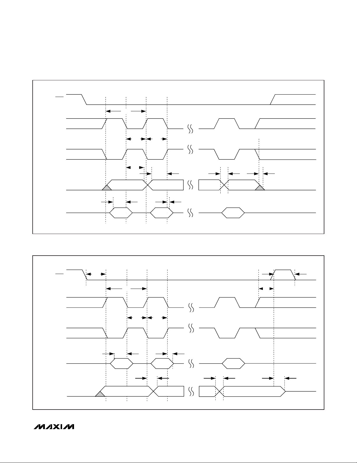
SPI (See Figures 1 and 2)
SPI Master Operating Frequency 1/t
SPI Slave Operating Frequency 1/t
SCLK Output Pulse-Width
High/Low
SCLK Input Pulse-Width
High/Low
t
MCH
t
SCH
MOSI Outp ut Hold T i me After
SCLK Sample Edge
MOSI Output Valid to Sample
Edge
MISO Input Valid to SCLK
Sample Edge Rise/Fall Setup
MISO Input to SCLK Sample
Edge Rise/ Fal l Ho ld
SCLK Inactive to MOSI Inactive t
SSEL Active to First Shift Edge t
MOSI Input to SCLK Sample
Edge Rise/Fall Setup
MOSI Input from SCLK Sample
Edge Transit ion Hold
MISO Output Valid After SCLK
Shift Edge Transit ion
SSEL Inactive t
SCLK Inactive to SSEL Rising t
MISO Output Di sabled After
SSEL Edge Rise
MCK
f
SCK
(t
/2)
, t
MCL
, t
t
SCL
CL = 50pF
t
MOH
t
MOV
25 ns
t
MIS
0 ns
t
MIH
MLH
4tCK ns
SSE
t
20 ns
SIS
t
SIH
t
SOV
SSH
SD
t
SLH
MCK
- 25
(t
MCK
- 25
(t
MCK
- 25
(t
MCK
- 25
tCK +
tCK +
tCK +
/2)
/2)
/2)
25
25
25
fCK/2 MHz
ns
/2 ns
SCK
ns
ns
ns
ns
3t
ns
ns
2t
/8 MHz
CK
+
CK
25
CK
50
+
ns
ns
Page 9
MAXQ2010
SSEL
SHIFT SHIFTSAMPLE SAMPLE
MOSI
MISO
SCLK
CKPOL/CKPHA
0/1 OR 1/0
SCLK
CKPOL/CKPHA
0/0 OR 1/1
t
SCH
t
SCL
t
SIS
t
SOV
t
RF
t
SD
t
SLH
t
SSH
t
SIH
t
SSE
t
SCK
MSB MSB-1
LSB
MSB LSBMSB-1
SSEL
SHIFT SHIFTSAMPLE SAMPLE
MOSI
MISO
SCLK
CKPOL/CKPHA
0/1 OR 1/0
SCLK
CKPOL/CKPHA
0/0 OR 1/1
t
MCK
t
MCH
t
MCL
t
MOH
t
MOV
t
MIS
t
MIH
t
MLH
t
RF
MSB MSB-1
MSB MSB-1
LSB
LSB
16-Bit Mixed-Signal Microcontroller with LCD
_______________________________________________________________________________________ 9
Figure 2. SPI Slave Timing
Figure 1. SPI Master Timing
Page 10
MAXQ2010
16-Bit Mixed-Signal Microcontroller with LCD
10 ______________________________________________________________________________________
I2C ELECTRICAL CHARACTERISTICS
(V
DVDD
= V
AVDD
= 2.7V to 3.6V, TA= -40°C to +85°C.)
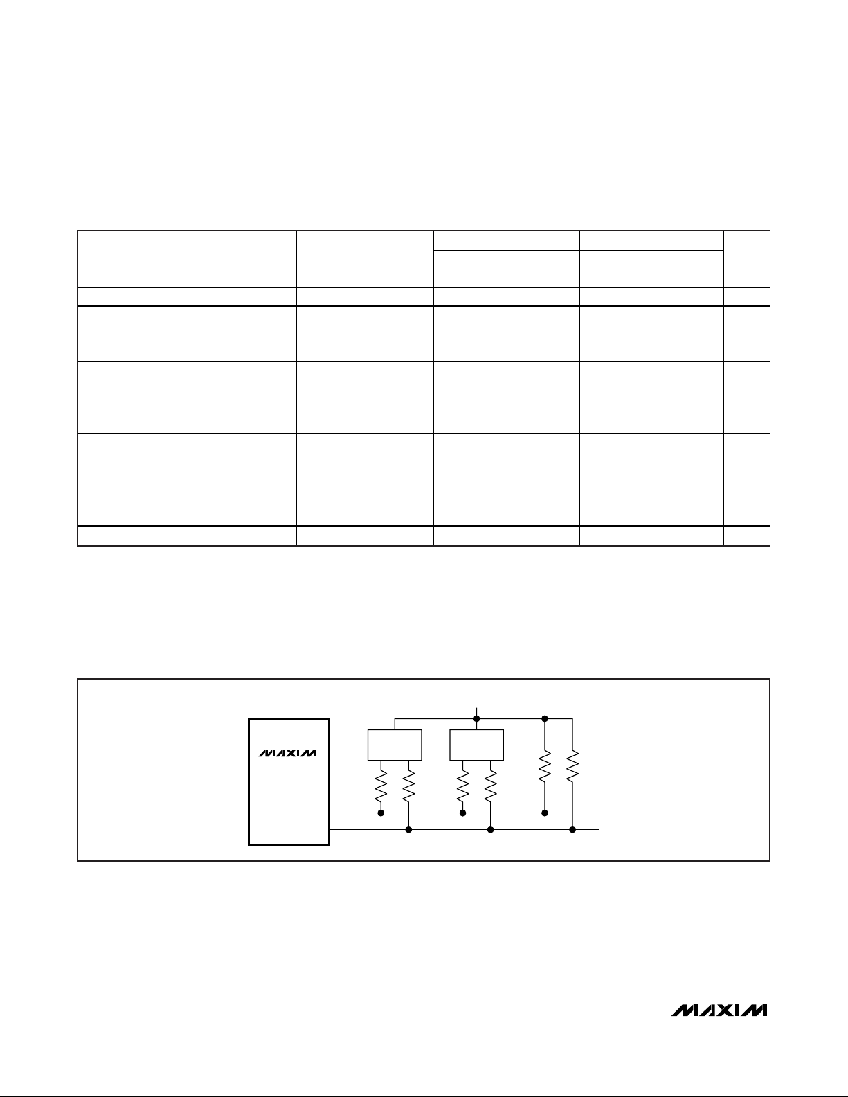
Note 19: Devices that use nonstandard supply voltages that do not conform to the intended I
2
C bus system levels must relate their
input levels to the voltage to which the pullup resistors R
P
are connected. See Figure 3.
Note 20: C
B
—Capacitance of one bus line in pF.
Note 21: The maximum fall time of 300ns for the SDA and SCL bus lines shown in the
I2C Bus Controller Timing
table is longer than
the specified maximum t
OF_I2C
of 250ns for the output stages. This allows series protection resistors (RS) to be connected
between the SDA/SCL pins and the SDA/SCL bus lines as shown in the
I2C Bus Controller Timing (Acting as I2C Slave)
table without exceeding the maximum specified fall time. See Figure 3.
SDA
P6.7
SCL
P6.6
RSR
S
I2C
DEVICE
RSR
S
I2C
DEVICE
RPR
P
V
DVDD
MAXQ2010
Figure 3. Series Resistors (RS) for Protecting Against High-Voltage Spikes
PARAMETER S YMBOL TEST CONDITIONS
Input Low Voltage (Note 19) V
Input High Voltage (Note 19) V
Input Hystere sis (Schmitt) V
Output Logic-Low (Open
Drain or Open Collector)
-0.5 0.3 x V
IL_I2C
0.7 x V
IH_I2C
IHYS_I2C VDVDD
V
OL_I2C
> 2V 0.05 x V
V
> 2V, 3mA s in k
DVDD
current
Output Fall Time from
to V
V
IH_MIN
Capacitance from 10pF to
IL_MAX
with Bus
250 20 + 0.1CB 250 ns
t
OF_I2C
400pF (Notes 20, 21)
Pulse Width of Spike
Filtering That Mu st Be
t
0 50 ns
SP_I2C
Suppressed by Input Filter
STANDARD MODE FAST MODE
MIN MAX MIN MAX
-0.5 0.3 x V
DVDD
0.7 x V
DVDD
DVDD VDVDD
V
DVDD
0 0.4 0 0.4 V
UNITS
V
DVDD
+ 0.5V V
Input Current on I/O I
I/O Capacitance C
IN_I2C
IO_I2C
Input voltage from 0.1 x
V
to 0.9 x V
DVDD
DVDD
-10 +10 -10 +10 μA
10 10 pF
Page 11

MAXQ2010
16-Bit Mixed-Signal Microcontroller with LCD
______________________________________________________________________________________ 11
I2C BUS CONTROLLER TIMING
(V
DVDD
= V
AVDD
= 2.7V to 3.6V, TA= -40°C to +85°C.) (Note 22) (Figure 4)
Note 22: All values referenced to V
IH_I2C(MIN)
and V
IL_I2C(MAX)
.
Note 23: A device must internally provide a hold time of at least 300ns for the SDA signal (referred to as the V
IH_I2C(MIN)
of the SCL
signal) to bridge the undefined region of the falling edge of SCL.
Note 24: The maximum t
HD:DAT
need only be met if the device does not stretch the low period (t
LOW_I2C
) of the SCL signal.
Note 25: A fast-mode I
2
C bus device can be used in a standard-mode I2C bus system, but the requirement t
SU:DAT
≥ 250ns must
be met. This is automatically the case if the device does not stretch the low period of the SCL signal. If such a device does
stretch the low period of the SCL signal, it must output the next data bit to the SDA line t
R_I2C(MAX)
+ t
SU:DAT
= 1000 + 250
= 1250ns (according to the standard-mode I
2
C specification) before the SCL line is released.
Note 26: C
B
—Total capacitance of one bus line in pF.
PARAMETER SYMBOL
Operating Frequency f
Hold Time After (Repeated)
START
Cloc k Low Period t
Clock High Period t
t
LOW_I2C
HIGH_I2C
Setup Time for Repeated START t
Hold Time for Data t
Setup Time for Data t
SDA/SCL Fall Time t
SDA/SCL Rise Time t
Setup Time for STOP t
Bus-Free Time Between STOP
and START
Capacitiv e Load for Each Bu s
Line
Noise Margin at the Low Level
for Each Connected Device
V
(Includ ing Hysteresis)
0 100 0 400 kHz
I2C
HD: STA
SU:STA
HD:DAT
SU:DAT
F_I2C
R_I2C
SU:STO
t
4.7 1.3 μs
BUF
C
400 400 pF
B
NL_I2C
STANDARD MODE FAST MODE
MIN MAX MIN MAX
4.0 0.6 μs
4.7 1.3 μs
4.0 0.6 μs
4.7 0.6 μs
0
(Note 23)
250
300
1000
3.45
(Note 24)
0
(Note 23)
100
(Note 25)
20 + 0.1C
(Note 26)
20 + 0.1C
(Note 26)
0.9
(Note 24)
ns
B
B
300 ns
300 ns
4.0 0.6 μs
0.1 x V
0.1 x V
DVDD
V
DVDD
UNITS
μs
Noise Margin at the High Level
for Each Connected Device
V
NH_I2C
0.2 x V
0.2 x V
DVDD
V
DVDD
(Includ ing Hysteresis)
Page 12

MAXQ2010
16-Bit Mixed-Signal Microcontroller with LCD
12 ______________________________________________________________________________________
I2C BUS CONTROLLER TIMING (ACTING AS I2C MASTER)
(V
DVDD
= V
AVDD
= 2.7V to 3.6V, TA= -40°C to +85°C.) (Figure 4)
PARAMETER SYMBOL
System Frequency f
Operating Frequency f
Hold Time After (Repeated)
START
Cloc k Low Period t
Clock High Period t
t
LOW_I2C
HIGH_I2C
Setup Time for Repeated START t
Hold Time for Data t
Setup Time for Data t
SDA/SCL Fall Time t
SDA/SCL Rise Time t
Setup Time for STOP t
Bus-Free Time Between STOP
and START
Capacitiv e Load for Each Bu s
Line
STANDARD MODE FAST MODE
MIN MAX MIN MAX
0.90 3.60 MHz
SYS
f
I2C
t
HD: STA
HIGH_I2C
5t
3t
t
SU:STA
0 3.45 0 0.9 μs
HD:DAT
250 100 ns
SU:DAT
300 20+ 0.1CB 300 ns
F_I2C
1000 20+ 0.1CB 300 ns
R_I2C
t
SU:STO
t
t
BUF
400 400 pF
C
B
LOW_I2C
HIGH_I2C
LOW_I2C
t
5t
SYS
3t
SYS
t
t
t
/8 f
SYS
HIGH_I2C
LOW_I2C
HIGH_I2C
LOW_I2C
μs
μs
SYS
μs
SYS
μs
μs
μs
SYS
UNITS
/8 Hz
Noise Margin at the Low Level
for Each Connected Device
(Includ ing Hysteresis)
Noise Margin at the High Level
for Each Connected Device
(Includ ing Hysteresis)
V
NL_I2C
V
NH_I2C
0.1 x V
0.2 x V
0.1 x V
DVDD
0.2 x V
DVDD
V
DVDD
V
DVDD
Page 13

MAXQ2010
16-Bit Mixed-Signal Microcontroller with LCD
______________________________________________________________________________________ 13
I2C BUS CONTROLLER TIMING (ACTING AS I2C SLAVE)
(V
DVDD
= V
AVDD
= 2.7V to 3.6V, TA= -40°C to +85°C.) (Figure 4)
Figure 4. I2C Bus Controller Timing Diagram
PARAMETER SYMBOL
System Frequency f
Operating Frequency f
System Clock Period t
Hold Time After (Repeated)
START
Cloc k Low Period t
Clock High Period t
t
LOW_I2C
HIGH_I2C
Setup Time for Repeated START t
Hold Time for Data t
Setup Time for Data t
SDA/SCL Fall Time t
SDA/SCL Rise Time t
Setup Time for STOP t
Bus-Free Time Between STOP
and START
Capacitiv e Load for Each Bu s
Line
Noise Margin at the Low Level
for Each Connected Device
V
(Includ ing Hysteresis)
STANDARD MODE FAST MODE
MIN MAX MIN MAX
0.9 3.60 MHz
SYS
f
I2C
1/f
SYS
3t
HD: STA
5t
3t
5t
SU:STA
0 3.45 0 0.9 μs
HD:DAT
250 100 ns
SU:DAT
300 20 + 0.1CB 300 ns
F_I2C
1000 20 + 0.1CB 300 ns
R_I2C
3t
SU:STO
t
5t
BUF
400 400 pF
C
B
0.1 x V
NL_I2C
1/f
I2C
3t
SYS
5t
SYS
3t
SYS
5t
SYS
3t
SYS
5t
SYS
0.1 x V
DVDD
/8 f
SYS
UNITS
/8 Hz
SYS
μs
I2C
μs
SYS
μs
SYS
μs
SYS
μs
SYS
μs
SYS
μs
SYS
V
DVDD
Noise Margin at the High Level
for Each Connected Device
V
NH_I2C
(Includ ing Hysteresis)
SSRPS
SDA
t
F_I2C
SCL
t
HD:STA
NOTE: TIMING REFERENCED TO V
t
IH_I2C(MIN)
LOW
AND V
t
HD:DAT
t
R_I2C
IL_I2C(MAX)
0.2 x V
t
SU:DAT
t
HIGH
.
0.2 x V
DVDD
t
SU:STA
V
DVDD
t
BUF
t
SU:STO
Page 14

MAXQ2010
16-Bit Mixed-Signal Microcontroller with LCD
14 ______________________________________________________________________________________
Typical Operating Characteristics
(TA = +25°C, unless otherwise noted.)
VDD SUPPLY CURRENT
vs. CLOCK FREQUENCY
3.5
CLOCK SOURCE DRIVEN ON HFXIN,
= +25°C, FLL DISABLED
T
A
3.0
2.5
(mA)
DD1
I
2.0
FREQMD = 1
1.5
1.0
010
f
HFXIN
INTEGRAL NONLINEARITY (INL)
vs. CODE
2.0
1.5
1.0
0.5
0
INL (LSB)
-0.5
-1.0
-1.5
-2.0
TA = +25°C, V
0
AVDD
= 3.3V, V
CODE
FREQMD = 0
(MHz)
REF
= 3.0V
PORT PIN LOW-OUTPUT VOLTAGE
vs. SINK CURRENT
40
TA = +25°C, V
35
MAXQ2010 toc01
30
25
(mA)
20
OH
I
15
10
5
0
8642
0 3.6
DVDD
= 3.6V
MAXQ2010 toc02
3.22.80.4 0.8 1.2 2.01.6 2.4
VOH (V)
DIFFERENTIAL NONLINEARITY (DNL)
vs. CODE
1.0
400030001000 2000
MAXQ2010 toc04
0.8
0.6
0.4
0.2
0
DNL (LSB)
-0.2
-0.4
-0.6
-0.8
-1.0
TA = +25°C, V
0
AVDD
= 3.3V, V
CODE
REF
= 3.0V
MAXQ2010 toc05
4000300020001000
PORT PIN HIGH-OUTPUT VOLTAGE
vs. SOURCE CURRENT
0
TA = +25°C, V
-10
-20
(mA)
-30
OH
I
-40
-50
-60
03.6
DVDD
= 3.6V
MAXQ2010 toc03
3.22.82.42.01.61.20.80.4
VOH (V)
OFFSET ERROR
vs. SUPPLY VOLTAGE
4
TA = +25°C, V
3
2
1
0
-1
OFFSET ERROR (LSB)
-2
-3
-4
2.96 3.66
REF
= 3.0V
V
DVDD
MAXQ2010 toc06
3.563.463.06 3.16 3.26 3.36
(V)
DIFFERENTIAL BIPOLAR TRANSFER
+FS = V
/2
7FF
7FE
001
000
FFF
OUTPUT CODE (HEX)
801
800
REF
/2
-FS = -V
REF
1 LSB = V
ZS = 0
/4096
REF
-FS + 0.5 LSB +FS - 0.5 LSB
INPUT VOLTAGE (LSB)
MAXQ2010 toc07
+FS0-FS
SINGLE-ENDED UNIPOLAR TRANSFER
FS = V
1 LSB = V
ZS = 0
REF
/4096
REF
INPUT VOLTAGE (LSB)
FFF
FFE
FFD
004
003
OUTPUT CODE (HEX)
002
001
000
FS - 0.5 LSB
FS2 3 41
MAXQ2010 toc08
Page 15

MAXQ2010
16-Bit Mixed-Signal Microcontroller with LCD
______________________________________________________________________________________ 15
Block Diagram
ADD REG
ADDRESS
GENERATOR
STACK
IP
DP
CONTROL
16
INSTRUCTION
DECODER
STATUS
DEMUX
SPR
Acc
SFR
IN-CIRCUIT
DEBUGGER
16
JTAG
MAXQ2010
MUX
PROGRAM
MEMORY
DATA
MEMORY
HFX
FLL
32kHz
PMM
STOP
TIMERUART
AVDD
AGND
SYSTEM
CLOCK
POWER
OSC UP
BROWNOUT
RESET
LCD
DVDD
DGND
RESET
I2CRTCSPI
12-BIT
8-CHANNEL
ADC
MACWATCHDOG
INTERRUPT
SUPPLY
VOLTAGE
MONITOR
Page 16

MAXQ2010
16-Bit Mixed-Signal Microcontroller with LCD
16 ______________________________________________________________________________________
Pin Description
PIN NAME FUNCTION
POWER PINS
40, 63, 96 DVDD Digital Supply Voltage
41, 66, 95 DGND Digital Ground
98, 99 REGOUT
82 AVDD Analog Supply Voltage
79 AGND Analog Ground
70 AVREF
78, 77 AN0, AN1
76, 75 AN2, AN3
74, 73 AN4, AN5
72, 71 AN6, AN7
92 RST
81 32KIN
80 32KOUT
64 HFXIN
65 HFXOUT
45 V
44 V
LCD1
LCD
Regulator Capacitor. These pins must be shorted together at the pins and then connected to
ground through a 1.0μF ceramic capacitor.
ANALOG MEASUREMENT PINS
Analog Voltage Reference. When using an external reference source, this pin must be
connected to 1μF and 0.01μF filter capacitors in parallel. When using an internal reference
source, this pin must be connected to a 0.01μF capacitor.
Analog Input 0:1. This pair of analog inputs can function as two single-ended inputs or one
different ial pair. When functioning in differential mode, AN0 is the positive input and AN1 i s
the negative input.
Analog Input 2:3. This pair of analog inputs can function as two single-ended inputs or one
different ial pair. When functioning in differential mode, AN2 is the positive input and AN3 i s
the negative input.
Analog Input 4:5. This pair of analog inputs can function as two single-ended inputs or one
different ial pair. When functioning in differential mode, AN4 is the positive input and AN5 i s
the negative input.
Analog Input 6:7. This pair of analog inputs can function as two single-ended inputs or one
different ial pair. When functioning in differential mode, AN6 is the positive input and AN7 i s
the negative input.
RESET PIN
Digital, Active-Low, Reset Input/Output. The CPU is held in reset when this pin is low and
begins executing from the reset vector when released. The pin includes pullup current source
and should be driven by an open-drain, external source capable of sinking in excess of 4mA.
This pin is driven low as an output when an internal reset condition occurs.
CLOCK PINS
32kHz Crystal Input/Output. Connect an external 6pF, 32 kH z watch crystal between 32KIN
and 32KOUT to generate the system clock. Alternatively, 32KIN is the input for an external
clock source when 32KOUT is disconnected.
High-Frequency Crystal Input. Connect an external crystal or resonator between HFXIN and
HFXOUT as the high-frequency system clock. Alternatively, HFXIN is the input for an external,
high-frequency cloc k source when HFXOUT is disconnected.
LCD PINS
LCD Bias Control Voltage. Highest LCD drive voltage used with static bias. Connected to an
external source.
LCD Bias, Voltage 1. LCD drive voltage u sed with 1/2 and 1/3 LCD bias. An internal res is tordivider sets the voltage. External resistors and capacitors can be used to change the LCD
voltage or drive capabilit y at this pin.
Page 17

MAXQ2010
16-Bit Mixed-Signal Microcontroller with LCD
______________________________________________________________________________________ 17
Pin Description (continued)
PIN NAME FUNCTION
LCD Bias, Voltage 2. LCD drive voltage u sed with 1/3 LCD b ias. An internal resistor-divider
43 V
42 V
6–1, 94, 93
91–84
LCD2
ADJ
GENERAL-PURPOSE I/O, SPECIAL FUNCTION, AND LCD INTERFACE PINS
P0.0–P0.7;
SEG0–SEG7;
INT0–INT7
P1.0–P1.7;
SEG8–SEG15
set s the voltage. External res istors and capacitors can be used to change LCD voltage or
drive capability at this pin.
LCD Adjustment Voltage. Connect to an external resistor to provide external control of the LCD
contrast. Leave disconnected for internal contrast adjustment.
Digital I/O, Type D Port 0; LCD Segment-Driver Output; External Edge-Selectable Interrupt.
This port functions as either bidirectional I/O or alternate LCD segment-drive outputs. The reset
condition of the port is with a ll bits at logic 1. In this state, a weak pullup holds the port high.
This condition serves as an input mode. Each port pin can individually be configured to act as
an external interrupt. Setting the PCF0 bit switches all pins on this port to LCD segment-drive
outputs.
It is possible to mix the LCD and interrupt functions on the same port. To do th is, the interrupt
enable must be e stablished prior to setting the PCF0 bit. Care must be taken not to enab le the
external interrupt while the LCD is in normal operational mode, as this could result in
potentially harmful contention between the LCD controller output and the external source
connected to the interrupt input.
PIN PORT S PECIAL/ALTERNATE FUNCTION
6 P0.0 SEG0 INT0
5 P0.1 SEG1 INT1
4 P0.2 SEG2 INT2
3 P0.3 SEG3 INT3
2 P0.4 SEG4 INT4
1 P0.5 SEG5 INT5
94 P0.6 SEG6 INT6
93 P0.7 SEG7 INT7
Digital I/O, Type C Port 1; LCD Segment-Driver Output. This port function s as either
bidirectional I/O or alternate LCD segment-drive outputs. The reset condition of the port is with
all bits at logic 1. In this state, a weak pullup holds the port high. This condition serves as an
input mode. The port pins also contain a Schmitt voltage input. Setting the PCF1 bit switches
all pins on this port to LCD segment-drive outputs.
PIN PORT S PECIAL/ALTERNATE FUNCTION
91 P1.0 SEG8
90 P1.1 SEG9
89 P1.2 SEG10
88 P1.3 SEG11
87 P1.4 SEG12
86 P1.5 SEG13
85 P1.6 SEG14
84 P1.7 SEG15
Page 18

MAXQ2010
16-Bit Mixed-Signal Microcontroller with LCD
18 ______________________________________________________________________________________
Pin Description (continued)
PIN NAME FUNCTION
Digital I/O, Type C Port 2; LCD Segment-Driver Output. This port function s as e ither
bidirectional I/O or alternate LCD segment-drive outputs. The reset condition of the port is with
all bits at logic 1. In this state, a weak pullup holds the port high. This condition serves as an
input mode. The port pins also contain a Schmitt voltage input. Setting the PCF2 bit switches
all pins on this port to LCD segment-drive outputs.
PIN PORT S PECIAL/ALTERNATE FUNCTION
56–52,
48–46
36–33, 22 –19
18–11
P2.0–P2.7;
SEG16–SEG23
P3.0–P3.7;
SEG24–SEG31
P4.0–P4.7;
SEG32–SEG39
Digital I/O, Type C Port 3; LCD Segment-Driver Output. This port function s as e ither
bidirectional I/O or alternate LCD segment-drive outputs. The reset condition of the port is with
all bits at logic 1. In this state, a weak pullup holds the port high. This condition serves as an
input mode. The port pins also contain a Schmitt voltage input. Setting the PCF3 bit switches
all pins on this port to LCD segment-drive outputs.
Digital I/O, Type-C Port 4; LCD Segment-Driver Output. This port functions as either
bidirectional I/O or alternate LCD segment-drive outputs. The reset condition of the port is with
all bits at logic 1. In this state, a weak pullup holds the port high. This condition serves as an
input mode. The port pins also contain a Schmitt voltage input. Setting the PCF4 bit switches
all pins on this port to LCD segment-drive outputs.
56 P2.0 SEG16
55 P2.1 SEG17
54 P2.2 SEG18
53 P2.3 SEG19
52 P2.4 SEG20
48 P2.5 SEG21
47 P2.6 SEG22
46 P2.7 SEG23
PIN PORT S PECIAL/ALTERNATE FUNCTION
36 P3.0 SEG24
35 P3.1 SEG25
34 P3.2 SEG26
33 P3.3 SEG27
22 P3.4 SEG28
21 P3.5 SEG29
20 P3.6 SEG30
19 P3.7 SEG31
PIN PORT S PECIAL/ALTERNATE FUNCTION
18 P4.0 SEG32
17 P4.1 SEG33
16 P4.2 SEG34
15 P4.3 SEG35
14 P4.4 SEG36
13 P4.5 SEG37
12 P4.6 SEG38
11 P4.7 SEG39
Page 19

MAXQ2010
16-Bit Mixed-Signal Microcontroller with LCD
______________________________________________________________________________________ 19
Pin Description (continued)
PIN NAME FUNCTION
LCD Segment-Driver Output; LCD Common Drive Output. These pins function as LCD
segment or common drive outputs. Configur ing a pin as a common drive output disables the
COM3, COM2,
10, 9, 8
7COM0 LCD Common Drive 0, Output. This pin functions as a LCD common-drive output.
68
67
61
60
59
58
57
32
31
COM1; SEG40,
SEG41, SEG41
P5.0/INT8/
TB0B/RX0
P5.1/INT9/
TB0A/TX0
P5.2/INT10/
SQW
P5.3/INT11/
SSEL
P5.4/INT12/
MOSI
P5.5/INT13/
SCLK
P5.6/INT14/
MISO
P6.0/INT15/
TCK
P6.1/INT16/
TDI
segment function for that pin.
PIN SPECIAL/ALTERNATE FUNCTION
10 COM3 SEG40
9 COM2 SEG41
8 COM1 SEG42
Digital I/O, Type D Port 5.0; Timer B0 Pin B; Serial Port 0 Receive; External Edge-Selectable
Interrupt 8. This pin defaults to an input with a weak pullup after reset and functions as
general-purpose I/O. The port pad contains a Schmitt voltage input and can be configured as
an external interrupt. Enabling a special function disables the pin a s digital I/O.
Digital I/O, Type D Port 5.1; Timer B0 Pin A; Serial Port 0 Transmit; External EdgeSelectable Interrupt 9. This pin defaults to an input with a weak pullup after reset and
function s as general-purpose I/O. The port pad contains a Schmitt voltage input and can be
configured as an external interrupt. Enabling a special function disables the pin as generalpurpose I/O.
Digital I/O, Type-D Port 5.2; External Edge-Selectable Interrupt 10; RTC Square-Wave Output.
Thi s pin defaults to an input with a weak pul lup after reset and functions as general-purpose
I/O. The port pad contains a Schmitt voltage input and can be configured as an external
interrupt. Enabling a special function disables the pin as general-purpose I/O.
Digital I/O, Type D Port 5.3; External Edge-Selectable Interrupt 11; Active-Low SPI SlaveSelect Input. This pin defaults to an input with a weak pullup after reset and function s a s
general-purpose I/O. The port pad contains a Schmitt voltage input and can be configured as
an external interrupt. Enabling a special function disables the pin a s general-purpose I/O.
Digital I/O, Type D Port 5.4; External Edge-Selectable Interrupt 12; SPI Master Out-Slave In
Output . This pin defaults to an input with a wea k pullup after reset and functions a s general-
purpose I/O. The port pad contains a Schmitt voltage input and can be configured as an
external interrupt. Enabling a special function disables the pin as general-purpose I/O.
Digital I/O, Type D Port 5.5; External Edge-Selectable Interrupt 13; SPI Clock Output. This pin
default s as an input with a weak pullup after a reset and functions a s general-purpose I/O. The
port pad contains a Schmitt input circuitry and can be configured as an external interrupt.
Enabling a special function disables the pin as general-purpose I/O.
Digital I/O, Type D Port 5.6; External Edge-Selectable Interrupt 14; SPI Master In-Slave
Output . This pin defaults to an input with a wea k pullup after reset and functions a s general-
purpose I/O. The port pad contains a Schmitt voltage input and can be configured as an
external interrupt. Enabling a special function disables the pin as general-purpose I/O.
Digital I/O, Type D Port 6.0; External Edge-Sel ectable Inter rupt 15; JTAG Test Clock Input.
Thi s pin defaults to an input with a weak pul lup after reset and functions as general-purpose
I/O. The port pad contains a Schmitt voltage input and can be configured as an external
interrupt. Enabling a special function disables the pin as general-purpose I/O.
Digital I/O, Type D Port 6.1; External Edge-Selectable Interrupt 16; JTAG Test Data Input.
Thi s pin defaults to an input with a weak pul lup after reset and functions as general-purpose
I/O. The port pad contains a Schmitt voltage input and can be configured as an external
interrupt. Enabling a special function disables the pin as general-purpose I/O.
Page 20

MAXQ2010
16-Bit Mixed-Signal Microcontroller with LCD
20 ______________________________________________________________________________________
Pin Description (continued)
PIN NAME FUNCTION
Digital I/O, Type D Port 6.2; External Edge-Selectable Interrupt 17; JTAG Test Mode Select
30
29
P6.2/INT17/
TMS
P6.3/INT18/
TDO
28
25
24
23
26, 27, 37, 38,
39, 49, 50, 51,
62, 69, 83, 97,
100
P6.4/INT19/
TB1B/RX1
P6.5/INT20/
TB1A/TX1
P6.6/INT21/
TB2B/SCL
P6.7/INT22/
TB2A/SDA
N.C. No Connection. Reserved for future use. Leave these pins unconnected.
Input. This pin defaults to an input with a weak pullup after reset and functions as generalpurpose I/O. The port pad contains a Schmitt voltage input and can be configured as an
external interrupt. Enabling a special function disables the pin as general-purpose I/O.
Digital I/O, Type-D Port 6.3; External Edge-Selectable Interrupt 18; JTAG Test Data Output.
Thi s pin defaults to an input with a weak pul lup after reset and functions as general-purpose
I/O. The port pad contains a Schmitt voltage input and can be configured as an external
interrupt. Enabling a special function disables the pin as general-purpose I/O.
Digital I/O, Type D Port 6.4; External Edge-Selectable Interrupt 19; Timer B1 Pin B; Serial
Port 1 Receive. This pin defaults to an input with a weak pullup after reset and functions as
general-purpose I/O. The port pad contains a Schmitt voltage input and can be configured as
an external interrupt. Enabling a special function disables the pin a s general-purpose I/O.
Digital I/O, Type D Port 6.5; External Edge-Selectable Interrupt 20; Timer B1 Pin A; Serial
Port 1 Transmit. This pin defaults to an input with a weak pullup after reset and functions as
general-purpose I/O. The port pad contains a Schmitt voltage input and can be configured as
an external interrupt. Enabling a special function disables the pin a s general-purpose I/O.
Digital I/O, Type D Port 6.6; External Edge-Selectable Interrupt 21; Timer B2 Pin B; I
I/O. This pin defaults to an input with a weak pullup after reset and functions as general-
purpose I/O. The port pad contains a Schmitt voltage input and can be configured as an
external interrupt. Enabling a special function disables the pin as general purpose I/O.
Digital I/O, Type D Port 6.7; External Edge-Selectable Interrupt 22; Timer B2 Pin A; I
I/O. This pin defaults to an input with a weak pullup after reset and functions as general-
purpose I/O. The port pad contains a Schmitt voltage input and can be configured as an
external interrupt. Enabling a special function disables the pin as general-purpose I/O.
NO CONNECTION PINS
2
C Clock
2
C Data
Page 21

MAXQ2010
16-Bit Mixed-Signal Microcontroller with LCD
______________________________________________________________________________________ 21
Detailed Description
The following sections are an introduction to the primary features of the microcontroller. More detailed
descriptions of the device features can be found in the
errata sheets and user’s guides described later in the
Additional Documentation
section.
MAXQ Core Architecture
The MAXQ2010 is a low-cost, high-performance,
CMOS, fully static, 16-bit RISC microcontroller with
flash memory and an integrated LCD controller. The
MAXQ2010 supports up to a 160-segment LCD and
supports 8 channels of high-performance measurement
using a 12-bit successive approximation register (SAR)
ADC with internal reference. The MAXQ2010 is structured on a highly advanced, accumulator-based, 16-bit
RISC architecture. Fetch and execution operations are
completed in one cycle without pipelining because the
instruction contains both the op code and data. The
result is a streamlined microcontroller performing at up
to one million instructions-per-second (MIPS) for each
MHz of the system operating frequency.
A 16-level hardware stack, enabling fast subroutine
calling and task switching, supports the highly efficient
core. Data can be quickly and efficiently manipulated
with three internal data pointers. Multiple data pointers
allow more than one function to access data memory
without having to save and restore data pointers each
time. The data pointers can automatically increment or
decrement following an operation, eliminating the need
for software intervention. As a result, application speed
is greatly increased.
Instruction Set
The instruction set is composed of fixed-length, 16-bit
instructions that operate on registers and memory locations. The instruction set is highly orthogonal, allowing
arithmetic and logical operations to use any register
along with the accumulator. Special-function registers
control the peripherals and are subdivided into register
modules. The family architecture is modular so that new
devices and modules can reuse code developed for
existing products.
The architecture is transport-triggered, which means
that writes or reads from certain register locations can
also cause side effects to occur. These side effects
form the basis for the higher level op codes defined by
the assembler, such as ADDC, OR, JUMP, etc. The op
codes are actually implemented as MOVE instructions
between certain register locations, while the assembler
handles the encoding, which need not be a concern to
the programmer.
The 16-bit instruction word is designed for efficient execution. Bit 15 indicates the format for the source field of
the instruction. Bits 0 to 7 of the instruction represent
the source for the transfer. Depending on the value of
the format field, this can either be an immediate value
or a source register. If this field represents a register,
the lower four bits contain the module specifier and the
upper four bits contain the register index in that module. Bits 8 to 14 represent the destination for the transfer. This value always represents a destination register,
with the lower four bits containing the module specifier
and the upper three bits containing the register
subindex within that module. Any time that it is necessary to directly select one of the upper 24 registers as a
destination, the prefix register (PFX) is needed to supply the extra destination bits. This prefix register write is
inserted automatically by the assembler and requires
only one additional execution cycle.
Memory Organization
The device incorporates several memory areas, including:
• 4KB utility ROM
• 64KB of flash memory for program storage
• 2KB of SRAM for storage of temporary variables
• 16-level stack memory for storage of program return
addresses and general-purpose use
The incorporation of flash memory allows the devices to
be reprogrammed multiple times, allowing modifications to user applications post production. Additionally,
the flash can be used to store application information
including configuration data and log files.
The default memory organization is organized as a
Harvard architecture, with separate address spaces for
program and data memory. Pseudo-Von Neumann
memory organization is supported through the utility
ROM for applications that require dynamic program
modification and execution from RAM. The pseudo-Von
Neumann memory organization places the code, data,
and utility ROM memories into a single contiguous
memory map. See Figure 5 for the memory map.
Stack Memory
A 16-bit-wide hardware stack provides storage for program return addresses and can also be used as general-purpose data storage. The stack is used
automatically by the processor when the CALL, RET,
and RETI instructions are executed and when an interrupt is serviced. An application can also store values in
the stack explicitly by using the PUSH, POP, and POPI
instructions.
Page 22

MAXQ2010
16-Bit Mixed-Signal Microcontroller with LCD
22 ______________________________________________________________________________________
On reset, the stack pointer, SP, initializes to the top of
the stack (0Fh). The CALL, PUSH, and interrupt-vectoring operations increment SP, then store a value at the
location pointed to by SP. The RET, RETI, POP, and
POPI operations retrieve the value at SP and then
decrement SP.
Utility ROM
The utility ROM is a 4KB block of internal ROM memory
that defaults to a starting address of 8000h. The utility
ROM consists of subroutines that can be called from
application software. These include the following:
• In-system programming (bootstrap loader) using
JTAG interface
• In-circuit debug routines
• Test routines (internal memory tests, memory loader,
etc.)
• User-callable routines for in-application flash programming and fast table lookup
Following any reset, execution begins in the utility ROM.
The ROM software determines whether the program
execution should immediately jump to location 0000h,
the start of user-application code, or to one of the special routines mentioned. Routines within the utility ROM
are user-accessible and can be called as subroutines
by the application software. More information on the
utility ROM contents is contained in the
MAXQ Family
User’s Guide: MAXQ2010 Supplement
.
Some applications require protection against unauthorized viewing of program code memory. For these
PROGRAM
SPACE
DATA
SPACE
2K x 16
UTILITY ROM
1K x 16
DATA RAM
32K x 16
PROGRAM
MEMORY
8000h
00h
0Fh
FFFFh
WBSn = 1
FFFFh
WBSn = 0
FFFFh
07FFh03FFh
0000h 0000h
87FFh
7FFFh
0000h
0Fh
07h
06h
00h
1Fh
SPRs
SFRs
REGISTERS
FFh
16 x 16
STACK
Figure 5. MAXQ2010 Default Memory Map
Page 23

MAXQ2010
16-Bit Mixed-Signal Microcontroller with LCD
______________________________________________________________________________________ 23
applications, access to in-system programming, inapplication programming, or in-circuit debugging functions is prohibited until a password has been supplied.
The password is defined as the 16 words of physical
program memory at addresses 0010h to 001Fh.
A single password lock (PWL) bit is implemented in the
SC register. When the PWL is set to 1 (power-on reset
default) and the contents of the memory at addresses
0010h to 001Fh are any value other than all FFh or 00h,
the password is required to access the utility ROM,
including in-circuit debug and in-system programming
routines that allow reading or writing of internal memory.
When PWL is cleared to 0, these utilities are fully accessible without the password. The password is automatically set to all 1s following a mass erase.
Programming
The microcontroller’s flash memory can be programmed by two different methods: in-system programming and in-application programming. Both methods
afford great flexibility in system design and reduce the
life-cycle cost of the embedded system. These features
can be password protected to prevent unauthorized
access to code memory.
(Bootloader) In-System Programming
An internal bootstrap loader allows the device to be
reloaded over a simple JTAG interface. As a result,
software can be upgraded in-system, eliminating the
need for a costly hardware retrofit when updates are
required. Remote software updates enable application
updates to physically inaccessible equipment. The
interface hardware can be a JTAG connection to another microcontroller, or a connection to a PC serial port
using a serial-to-JTAG converter such as the MAXQJTAG-001, available from Maxim. If in-system programmability is not required, use a commercial gang
programmer for mass programming.
Activating the JTAG interface and loading the test
access port (TAP) with the system programming
instruction invokes the bootstrap loader. Setting the SPE
bit to 1 during reset through the JTAG interface executes the bootstrap-loader-mode program that resides
in the utility ROM. When programming is complete, the
bootstrap loader can clear the SPE bit and reset the
device, allowing the device to bypass the utility ROM
and begin execution of the application software.
The following bootstrap loader functions are supported:
• Load • Verify
• Dump • Erase
• CRC
In-Application Programming
The in-application programming feature allows the
microcontroller to modify its own flash program memory
while simultaneously executing its application software.
This allows on-the-fly software updates in mission-critical applications that cannot afford downtime.
Alternatively, it allows the application to develop custom loader software that can operate under the control
of the application software. The utility ROM contains
user-accessible flash programming functions that erase
and program flash memory. These functions are
described in detail in the
MAXQ Family User’s Guide:
MAXQ2010 Supplement
.
Register Set
Most functions of the device are controlled by sets of
registers. These registers provide a working space for
memory operations as well as configuring and addressing peripheral registers on the device. Registers are
divided into two major types: system registers and
peripheral registers. The common register set, also
known as the system registers, includes the ALU, accumulator registers, data pointers, interrupt vectors and
control, and stack pointer. The peripheral registers
define additional functionality that may be included by
different products based on the MAXQ architecture.
This functionality is broken up into discrete modules so
that only the features required for a given product need
to be included.
The documentation on the module and register functions is covered fully in the
MAXQ Family User’s Guide
and the
MAXQ Family User’s Guide: MAXQ2010
Supplement
. This information includes the locations of
status and control bits and a detailed description of
their function and reset values. Refer to these documents for a complete understanding of the features and
operation of the microcontroller.
System Timing
For maximum versatility, the device can generate its
internal system clock from several sources:
• External clock source
• Internal oscillator using external crystal or resonator
• FLL using 32kHz clock source (approximately 8MHz)
• FLL with no external crystal (approximately 5MHz)
Operation from an external clock source or internal
oscillator using external crystal or resonator is similar to
other microcontrollers. The designer must remember
that the rated maximum speed of operation applies to
the speed of the microcontroller core, not the external
Page 24

MAXQ2010
16-Bit Mixed-Signal Microcontroller with LCD
24 ______________________________________________________________________________________
clock source. The device contains an FLL that is used
as a clock source by itself (FLLEN = 0) or as a multiplier for the 32kHz crystal (FLLEN = 1). The 32kHz-modebased timing is more stable due to the use of the
crystal as a time base.
A crystal warmup counter enhances operational reliability. If the user has selected to run from the external
crystal or clock source, each time the external crystal
oscillation must restart, such as after exiting stop mode,
the device initiates a crystal warmup period of 65,536
oscillations. This allows time for the crystal amplitude
and frequency to stabilize before using it as a clock
source. While in the warmup mode, the device operates
from the internal FLL and automatically switches back
to the crystal as soon as it is ready.
Programmable clock-divide control bits (CD1 and CD0)
and the PMME bit provide the processor with the ability
to slow the system clock, resulting in lower power consumption. The CD[1:0] bits default to 00b, selecting a
divide-by-1 system clock, but five clock-divisor options
allow the selection of different crystals to accommodate
specific system needs. In power-management mode
(PMM), one system clock is 256 oscillator cycles, significantly reducing power consumption while the microcontroller functions at reduced speed. The switchback
feature allows the system to exit PMM in response to an
external interrupt or serial port activity, quickly switching from the slower, power-saving mode to full speed.
In addition, the lowest power stop mode allows the
microcontroller to stop the internal oscillator, halting the
system clock.
Interrupts
Multiple interrupt sources are available for quick
response to internal and external events. The MAXQ
architecture uses a single interrupt vector (IV), single
interrupt-service routine (ISR) design. For maximum flexibility, interrupts can be enabled globally, individually, or
by the module. When an interrupt condition occurs, its
individual flag is set, even if the interrupt source is disabled at the local, module, or global level. Interrupt
flags must be cleared within the user-interrupt routine to
avoid repeated interrupts from the same source.
Application software must ensure a delay between the
write to the flag and the RETI instruction to allow time
for the interrupt hardware to remove the internal interrupt condition. Asynchronous interrupt flags require a
one-instruction delay, and synchronous interrupt flags
require a two-instruction delay.
When an enabled interrupt is detected, software jumps
to a user-programmable interrupt vector location. The
IV register defaults to 0000h on reset or power-up, so if
it is not changed to a different address, the user program must determine whether a jump to 0000h came
from a reset or interrupt source.
Once software control has been transferred to the ISR,
the interrupt identification register (IIR) can be used to
determine if a system register or peripheral register was
the source of the interrupt. The specified module can
then be interrogated for the specific interrupt source and
software can take appropriate action. Because the user
software evaluates the interrupts, the user can define a
unique interrupt priority scheme for each application.
The following interrupt sources are supported:
• Supply Voltage Monitor
• External Interrupts 22 to 0
• Timer 2, 1, 0
• Serial Port 1, 0
• Watchdog Timer
• RTC Time-of-Day or Subsecond Alarm
• SPI
• I
2
C
• ADC
When an enabled interrupt is detected, software jumps
to the dedicated interrupt vector address reserved for
that interrupt. User-application code at this address
then routes program execution to a user-defined interrupt routine.
I/O Ports
The microcontroller uses Type C and Type D bidirectional I/O pins as described in the
MAXQ Family User's
Guide
. Each port has up to eight independent, generalpurpose I/O pins and three configure/control registers.
Many pins support alternate functions such as timers or
interrupts, which are enabled, controlled, and monitored
by dedicated peripheral registers. Using the alternate
function automatically converts the pin to that function,
overriding the general-purpose I/O functionality.
Type C port pins have Schmitt trigger receivers and full
CMOS output drivers, and can support alternate functions. The pin is either high impedance or a weak
pullup when defined as an input, dependent on the
state of the corresponding bit in the output register.
Type D port pins have Schmitt trigger receivers and full
CMOS output drivers, and can support alternate functions. The pin is either high impedance or a weak
pullup when defined as an input, dependent on the
state of the corresponding bit in the output register. All
Type D pins also have interrupt capability. See Figure 6
for a Type C/D port pin schematic.
Page 25

MAXQ2010
16-Bit Mixed-Signal Microcontroller with LCD
______________________________________________________________________________________ 25
Supply Voltage Monitor
The supply voltage monitor can detect if the supply voltage has fallen below a user-selectable level. If this happens, the microcontroller can be programmed to
generate an interrupt to inform the system. The detection level is set using the supply voltage threshold bit
(SVMTH) and can be adjusted from 2.7V to 3.5V in 0.1V
increments. Setting the SVMEN bit to 1 enables the supply voltage monitor. Once the monitoring circuitry is stable and ready for operation, the supply voltage monitor
ready (SVMRDY) flag is set to 1. The default set point is
2.7V (SVTH[3:0] = 07h). Care must be taken not to set
the set point below 2.7V as SVM interrupts may not
occur because the brownout monitor may activate first.
The supply voltage monitor causes a switchback to
occur if the supply voltage falls below the threshold
value and the supply voltage monitor interrupt is
enabled (SVMIE = 1).
The supply voltage monitor remains operational in stop
mode if the supply voltage monitor stop mode enable
bit (SVMSTOP) is set to 1. Clearing SVMSTOP to 0 disables the supply voltage monitor on entry to stop mode
if the SVM peripheral is enabled. If the supply voltage
monitor is enabled during stop mode, an SVMI interrupt
causes the processor to exit stop mode if enabled
(SVMIE = 1).
Serial Peripherals
The microcontroller supports two independent USARTs
as well as I2C master/slave and SPI master communication ports.
USART Serial Ports
The independent USARTs provide transmit and receive
signals to communicate with other RS-232 interfaceenabled devices, as well as PCs and serial modems
when paired with an external RS-232 line driver/receiver.
The dual independent USARTs can communicate simultaneously at different baud rates with two separate peripherals. The USART can detect framing errors and indicate
the condition through a user-accessible software bit.
PD.x
SF DIRECTION
SF ENABLE
MUXMUX
PO.x
V
DDIO
SF OUTPUT
V
DDIO
WEAK
I/O PAD
PORT PIN
INTERRUPT
FLAG
FLAG
PI.x OR SF INPUT
EIES.x
TYPE D PORT ONLY
DETECT
CIRCUIT
MAXQ2010
Figure 6. Type C/D Port Pin Schematic
Page 26

MAXQ2010
16-Bit Mixed-Signal Microcontroller with LCD
26 ______________________________________________________________________________________
The time base of the serial ports is derived from either a
division of the system clock or the dedicated baudclock generator. Table 1 summarizes the operating
characteristics of each mode.
Real-Time Clock
A binary real-time clock (RTC) keeps the time of day in
absolute seconds with 1/256-second resolution. The
32-bit second counter can count up to approximately
136 years and be translated to calendar format by
application software. A time-of-day alarm and independent subsecond alarm can cause an interrupt or wake
the device from stop mode.
The independent subsecond alarm runs from the same
RTC and allows the application to support interrupts
with a minimum interval of approximately 3.9ms. This
creates an additional timer that can be used to measure long periods of time without performance degradation. Traditionally, long time periods have been
measured using multiple interrupts from shorter interrupt intervals. Each timer interrupt required servicing,
with each accompanying interruption slowing system
operation. By using the RTC subsecond timer as a
long-period timer, only one interrupt is needed, eliminating the performance hit associated with using a
shorter timer.
An internal crystal oscillator clocks the RTC using integrated 6pF load capacitors, and yields the best performance when mated with a 32.768kHz crystal rated for a
6pF load. No external load capacitors are required.
Higher accuracy can be obtained by supplying an
external clock source to the RTC.
Programmable Timers
The microcontroller incorporates three instances of the
16-bit programmable Timer/Counter B peripheral,
denoted TB0, TB1, and TB2. They can be used in
counter/timer/capture/compare/PWM functions, allow-
ing precise control of internal and external events.
These timer/counters support clock input prescaling
and set/reset/toggle PWM/output control functionality
not found on other MAXQ timer implementations. A new
register, TBC, supports certain PWM/output control
functions in some implementations. A distinguishing
characteristic of Timer/Counter B is that its count
ranges from 0000h to the value stored in the 16-bit capture/reload register (TBR), whereas in other implementations (e.g., Timer 1) the count ranges from the value
in the reload register to FFFFh. These timers are fully
described in the
MAXQ Family User’s Guide
.
Timer B operational modes include the following:
• Autoreload
• Autoreload Using External Pin
• Capture Using External Pin
• Up/Down Count Using External Pin
• Up-Count PWM/Output
• Up/Down PWM/Output
• Clock Output on TBB Pin
Watchdog Timer
An internal watchdog timer greatly increases system reliability. The timer resets the device if software execution
is disturbed. The watchdog timer is a free-running
counter designed to be periodically reset by the application software. If software is operating correctly, the
counter is periodically reset and never reaches its maximum count. However, if software operation is interrupted,
the timer does not reset, triggering a system reset and
optionally a watchdog timer interrupt. This protects the
system against electrical noise or electrostatic discharge
(ESD) upsets that could cause uncontrolled processor
operation. The internal watchdog timer is an upgrade to
older designs with external watchdog devices, reducing
system cost and simultaneously increasing reliability.
Table 1. Serial Port Operating Characteristics
MODE TYPE START BITS DATA BITS STOP BIT
Mode 0 Synchronous — 8 —
Mode 1 Asy nchronou s 1 8 1
Mode 2 Asynchronous 1 8 + 1 1
Mode 3 Asynchronous 1 8 + 1 1
Page 27

MAXQ2010
16-Bit Mixed-Signal Microcontroller with LCD
______________________________________________________________________________________ 27
The watchdog timer is controlled through bits in the
WDCN register. Its timeout period can be set to one of
four programmable intervals ranging from 212to 2
21
system clocks in its default mode, allowing flexibility to
support different types of applications. The interrupt
occurs 512 system clocks before the reset, allowing the
system to execute an interrupt and place the system in
a known, safe state before the device performs a total
system reset. At 8MHz, watchdog timeout periods can
be programmed from 512µs to 67s, depending on the
system clock mode.
Hardware Multiplier
The internal hardware multiplier supports high-speed
multiplications. The multiplier can complete a 16-bit x
16-bit multiply-and-accumulate/subtract operation in a
single cycle with the support of a 48-bit accumulator.
The multiplier is a fixed-point arithmetic unit. The
operands can be either signed or unsigned numbers,
but the data type must be defined by the application
software prior to loading the operand registers.
Seven different multiply operations can be performed
without requiring direct intervention of the microcontroller core. These include the following:
• Unsigned 16-bit multiplication
• Unsigned 16-bit multiplication and accumulation
• Unsigned 16-bit multiplication and subtraction
• Signed 16-bit multiplication
• Signed 16-bit multiplication and negate
• Signed 16-bit multiplication and accumulation
• Signed 16-bit multiplication and subtraction
Each of these operations is controlled and accessed
through six SFR registers. The 8-bit multiplier control
register (MCNT) selects the operation, data type,
operand count, optional hardware-based square function, write option on the MC register, the overflow flag,
and the clear control for operand registers and accumulator. Loading and unloading of the data is achieved
through five 16-bit SFR registers.
Only one cycle is needed for computation. This means
that the result of an operation is ready in the next cycle
immediately following the loading of the last operand.
Back-to-back operations can be performed without wait
states between operations, independent of data type
and operand count.
Analog-to-Digital Converter
The MAXQ2010 contains a 12-bit successive approximation analog-to-digital converter (ADC) with an analog
mux (Figure 7). The mux selects the ADC input from
eight single-ended channels or four differential channels. An internal precision bandgap reference can be
used for the ADC reference voltage, or the reference
voltage can be externally driven. Additionally, the analog supply voltage (AV
DD
) can also be used as the voltage reference. The ADC runs off a 2.7V to 3.6V power
supply and at a conversion rate up to 300ksps.
The ADC block includes a 12-bit SAR core, ADC controls, a reference generator, and a circular block of sixteen 12-bit data buffers. The ADC is controlled by SFR
registers. An autoscan feature allows the user to select
up to eight sampling channels for storage in the 16
memory locations.
There are two conversion modes: single-sequence
mode and continuous-sequence mode.
The ADC’s internal power-management system automatically powers down when the conversion(s) are
done (ADCONV = 0). The start conversion bit,
ADCONV, is used to start all conversion processes. If
the ADC power-management override bit is cleared
(ADPMO = 0), the ADC waits for 20 ADCCLK before
starting the first conversion. This allows the ADC time to
set up.
If ADPMO = 1, an ADC conversion is initiated as soon
as ADCONV is set to 1. ADC operation is aborted upon
entry into PMM or stop mode.
The ADCONV bit is set at the beginning of the conversion process and remains set until the conversion
process is finished. In single-sequence mode, this bit
remains set until the ADC has finished conversion on
the last channel in the sequence. In continuous mode,
the ADCONV bit remains set until the continuous mode
is stopped. Writing a 0 to the ADCONV bit stops ADC
operation at the completion of the current ADC conversion. The new data is written to the data buffer.
An A/D conversion takes 16 ADCCLK cycles to complete. Three of the 16 ADCCLK cycles are used for
sample acquisition. The ADCCLK is derived from the
system clock with divide ratio defined by the ADC clock
divider bits (ADCCLK). Therefore, with 16 ADCCLK to
acquire one data, the fastest ADC rate = sysclk/16
(ADCCLK = 0h, ADACQEN = 0h). With a 10MHz system clock, this is theoretically equivalent to 10MHz/16
value Msps. Note, however, that the ADC conversion is
limited to 300ksps.
If the ADC data-available interrupt is enabled (ADDAIE
= 1), an interrupt is generated to the CPU when ADDAI
= 1. Once set, the ADADI flag can be cleared by software writing a 0 or at the start of a conversion process
when ADCONV is set to 1. The data-available interrupt
flag (ADDAI) can optionally be set by using the ADC
Page 28

MAXQ2010
16-Bit Mixed-Signal Microcontroller with LCD
28 ______________________________________________________________________________________
data-available interrupt interval bits (ADDAINV). The
ADDAI can be set in 1, 2, 3, 4, 5, 6, 7, 8, 12, or 16 samples intervals. For a sequence that uses only one configuration register, setting ADDAINV = 00 generates an
interrupt with the same interval as ADDAINV = 01, both
of which set the ADDAI at every ADC sample. When the
ADDAI is set, the last memory location written by ADC
will also be written to ADDADDR.
LCD Controller
The MAXQ2010 microcontroller incorporates an LCD
controller that interfaces to common low-voltage displays. By incorporating the LCD controller into the
microcontroller, the design requires only an LCD glass
rather than a considerably more expensive LCD module. Every character in an LCD glass is composed of
one or more segments, each of which is activated by
selecting the appropriate segment and common signal.
The microcontroller can multiplex combinations of up to
43 segment outputs (SEG0 to SEG42) and four common signal outputs (COM0 to COM3). Unused segment
outputs can be used as general-purpose port pins.
The segments are easily addressed by writing to dedicated display memory. Once the LCD controller settings and display memory have been initialized, the
21-byte display memory is periodically scanned, and
the segment and common signals are generated automatically at the selected display frequency. No additional processor overhead is required while the LCD
controller is running. Unused display memory can be
used for general-purpose storage.
The design is further simplified and cost reduced by
the inclusion of software-adjustable internal voltagedividers to control display contrast, using either V
DDIO
or an external voltage. If desired, contrast can also be
controlled with an external resistance. The features of
the LCD controller include the following:
• Automatic LCD segment and common-drive signal
generation
• Four display modes supported:
Static (COM0)
1/2 duty multiplexed with 1/2 bias voltages (COM[0:1])
1/3 duty multiplexed with 1/3 bias voltages (COM[0:2])
1/4 duty multiplexed with 1/3 bias voltages (COM[0:3])
• Up to 43 segment outputs and four common-signal
outputs
• 21 bytes (168 bits) of display memory
• Flexible LCD clock source, selectable from 32kHz or
HFClk/512
• Adjustable frame frequency
• Internal voltage-divider resistors eliminate require-
ment for external components
• Internal adjustable resistor allows contrast adjustment
without external components
INPUT
MULTIPLEXER
AND
TRACK/HOLD
12-BIT
SAR
INTERNAL
REFERENCE
EXTERNAL
REFERENCE
AVDD
ADC REFERENCE
ADC CONTROL
AN7
AVDD
AVSS
ADC INTERRUPT
AN6
AN5
AN4
AN3
AN2
AN1
AN0
Figure 7. ADC Block Diagram
Page 29

MAXQ2010
16-Bit Mixed-Signal Microcontroller with LCD
______________________________________________________________________________________ 29
A simple LCD-segmented glass interface example
demonstrates the minimal hardware required to interface to a MAXQ2010 microcontroller. A two-character
LCD is controlled, with each character containing
seven segments plus decimal point. The LCD controller
is configured for 1/2 duty-cycle operation, meaning the
active segment is controlled using a combination of
segment signals and COM0 or COM1 signals are used
to select the active display. See Figure 8.
In-Circuit Debug
Embedded debugging capability is available through
the JTAG-compatible TAP. Embedded debug hardware
and embedded ROM firmware provide in-circuit debugging capability to the user application, eliminating the
need for an expensive in-circuit emulator. Figure 9
shows a block diagram of the in-circuit debugger. The
in-circuit debug features include the following:
• A hardware debug engine.
• A set of registers able to set breakpoints on register,
code, or data accesses.
• A set of debug service routines stored in the utility
ROM.
The embedded hardware debug engine is an independent hardware block in the microcontroller. The debug
TAP
CONTROLLER
CPU
DEBUG
ENGINE
DEBUG
SERVICE
ROUTINES
(UTILITY ROM)
CONTROL
BREAKPOINT
ADDRESS
DATA
TMS
TCK
TDI
TDO
MAXQ2010
Figure 9. In-Circuit Debugger
SEG0
SEG1
SEG2
SEG3
COM0
SEG[0:7]
CONNECTED TO DARK GREY SEGMENTS
COM1
CONNECTED TO LIGHT GREY SEGMENTS
SEG4
SEG5
SEG6
SEG7
MAXQ2010
Figure 8. Two-Character, 1/2 Duty, LCD Interface Example
Page 30

MAXQ2010
16-Bit Mixed-Signal Microcontroller with LCD
30 ______________________________________________________________________________________
engine can monitor internal activities and interact with
selected internal registers while the CPU is executing
user code. Collectively, the hardware and software features allow two basic modes of in-circuit debugging:
• Background mode allows the host to configure and
set up the in-circuit debugger while the CPU continues to execute the application software at full speed.
Debug mode can be invoked from background mode.
• Debug mode allows the debug engine to take control
of the CPU, providing read/write access to internal registers and memory, and single-step trace operation.
Applications Information
The low-power, high-performance RISC architecture of
this device makes it an excellent fit for many portable or
battery-powered applications that require cost-effective
computing. The high-throughput core is complemented
by a 16-bit hardware multiplier-accumulator, allowing
the implementation of sophisticated computational
algorithms. Applications benefit from a wide range of
peripheral interfaces, allowing the microcontroller to
communicate with many external devices. With integrated LCD support of up to 160 segments, applications
can support complex user interfaces. Displays are driven directly with no additional external hardware
required. Contrast can be adjusted using a built-in,
adjustable resistor. The simplified architecture reduces
component count and board space, critical factors in
the design of portable systems.
The MAXQ2010 is ideally suited for applications such
as medical instrumentation, portable blood-glucose
equipment, and data-collection devices. For blood-glucose measurement, the microcontroller integrates an
SPI interface that directly connects with analog frontends for measuring test strips.
Grounds and Bypassing
Careful PCB layout significantly minimizes noise on the
analog inputs, resulting in less noise on the digital I/O
that could cause improper operation. The use of multilayer boards is essential to allow the use of dedicated
power planes. The area under any digital components
should be a continuous ground plane if possible. Keep
any bypass capacitor leads short for best noise rejection and place the capacitors as close to the leads of
the devices as possible.
Separate ground areas must be provided for the analog
(AGND) and digital (DGND) portions, connected
together at a single point.
CMOS design guidelines for any semiconductor require
that no pin be taken above V
DVDD
or below DGND.
Violation of this guideline can result in a hard failure
(damage to the silicon inside the device) or a soft failure
(unintentional modification of memory contents). Voltage
spikes above or below the device’s absolute maximum
ratings can potentially cause a devastating IC latchup.
Microcontrollers commonly experience negative voltage spikes through either their power pins or generalpurpose I/O pins. Negative voltage spikes on power
pins are especially problematic as they directly couple
to the internal power buses. Devices such as keypads
can conduct electrostatic discharges directly into the
microcontroller and seriously damage the device.
System designers must protect components against
these transients that can corrupt system memory.
Additional Documentation
Designers must have four documents to fully use all the
features of this device. This data sheet contains pin
descriptions, feature overviews, and electrical specifications. Errata sheets contain deviations from published specifications. The user’s guides offer detailed
information about device features and operation. The
following documents can be downloaded from
www.maxim-ic.com/microcontrollers.
• This MAXQ2010 data sheet, which contains electrical/timing specifications and pin descriptions.
• The MAXQ2010 revision-specific errata sheet
(www.maxim-ic.com/errata).
• The
MAXQ Family User's Guide
, which contains detailed
information on core features and operation, including
programming (www.maxim-ic.com/MAXQUG).
• The
MAXQ Family User's Guide: MAXQ2010 Supplement
,
which contains detailed information on features specific to the MAXQ2010.
Development and Technical
Support
Maxim and third-party suppliers provide a variety of
highly versatile, affordably priced development tools for
this microcontroller, including the following:
• Compilers
• In-circuit emulators
• Integrated Development Environments (IDEs)
• JTAG-to-serial converters for programming and
debugging
A partial list of development tool vendors can be found
at www.maxim-ic.com/MAXQ_tools
.
For technical support, go to www.maxim-ic.com/support.
Page 31

MAXQ2010
16-Bit Mixed-Signal Microcontroller with LCD
______________________________________________________________________________________ 31
Pin Configuration
AN3P0.5/SEG5/INT5
1 75
AN4P0.4/SEG4/INT4
2 74
AN5P0.3/SEG3/INT3
3 73
AN6P0.2/SEG2/INT2
4 72
AN7P0.1/SEG1/INT1
5 71
N.C.COM0
7 69
P5.0/INT8/TB0B/RX0COM1/SEG42
8 68
P5.1/INT9/TB0A/TX0COM2/SEG41
9 67
N.C.P6.5/INT20/TB1A/TX1
25 51
TOP VIEW
AVREF
6 70
P0.0/SEG0/INT0
HFXOUT
11 65
P4.7/SEG39
HFXIN
12 64
P4.6/SEG38
DVDD
13 63
P4.5/SEG37
P5.2/INT10/SQW
15 61
P4.3/SEG35
P5.3/INT11/SSEL
16 60
P4.2/SEG34
P5.4/INT12/MOSI
17 59
P4.1/SEG33
DGND
10 66
COM3/SEG40
N.C.
14 62
P4.4/SEG36
P5.5/INT13/SCLK
18 58
P4.0/SEG32
P5.6/INT14/MISO
19 57
P3.7/SEG31
P2.0/SEG16
20 56
P3.6/SEG30
P2.2/SEG18
22 54
P3.4/SEG28
P2.3/SEG19
23 53
P6.7/INT22/TB2A/SDA
P2.4/SEG20
24 52
P6.6/INT21/TB2B/SCL
P2.1/SEG17
21 55
P3.5/SEG29
LQFP
26
100
N.C. N.C.
27
99
N.C. REGOUT
28
98
P6.4/INT19/TB1B/RX1 REGOUT
29
97
P6.3/INT18/TDO N.C.
30
96
P6.2/INT17/TMS DVDD
31
95
P6.1/INT16/TDI DGND
32
94
P6.0/INT15/TCK P0.6/SEG6/INT6
33
93
P0.7/SEG7/INT7P3.3/SEG27
34
92
P3.2/SEG26 RST
35
91
P1.0/SEG8P3.1/SEG25
36
90
P1.1/SEG9P3.0/SEG24
37
89
P1.2/SEG10N.C.
38
88
P1.3/SEG11N.C.
39
87
P1.4/SEG12N.C.
40
86
P1.5/SEG13DVDD
41
85
DGND P1.6/SEG14
42
84
P1.7/SEG15
V
ADJ
43
83
N.C.
V
LCD2
44
82
AVDD
V
LCD1
45
81
32KIN
V
LCD
46
80
32KOUTP2.7/SEG23
47
79
AGNDP2.6/SEG22
48
78
AN0P2.5/SEG21
49
77
AN1N.C.
50
76
N.C. AN2
+
MAXQ2010
Page 32

MAXQ2010
16-Bit Mixed-Signal Microcontroller with LCD
32 ______________________________________________________________________________________
Typical Application Circuit
AVDD
AGND
DVDD
DGND
AN0
AN1
AN2
AN3
AN4
AN5
AN6
AN7
RST
32KIN
32KOUT
AVREF
OPTIONAL
EXTERNAL
REFERENCE
COM3
COM2
COM1
COM0
RX0
TX0
RX1
TX1
UP TO 40
SEG PINS
UP TO 55
DIGITAL I/O PINS
JTAG PINS
10nF
32.768kHz
HFXIN
OPTIONAL
HFXOUT
10MHz
22pF
1μF
22pF
1kΩ
REGOUT
1μF
LCD SEGMENT PINS
160-SEGMENT LCD DISPLAY
SCL
SDA
SSEL
MOSI
SCLK
MISO
SERIAL 0
SERIAL 1
HOST INTERFACE
MAXQ2010
RS-232
TRANSCEIVER
MAX3233E
FOUR CURRENT SOURCES
CAPABLE OF SINKING OR
SOURCING CURRENT*
*APPLICATION DEPENDENT.
JTAG
INTERFACE
HOST INTERFACE
DS4404
DUAL AUDIO TAPER
POTENTIOMETER
WITH PUSHBUTTON
CONTROL*
DS1802
Page 33

MAXQ2010
16-Bit Mixed-Signal Microcontroller with LCD
Maxim cannot assume responsibility for use of any circuitry other than circuitry entirely embodied in a Maxim product. No circuit patent licenses are
implied. Maxim reserves the right to change the circuitry and specifications without notice at any time.
Maxim Integrated Products, 120 San Gabriel Drive, Sunnyvale, CA 94086 408-737-7600 ____________________
33
© 2008 Maxim Integrated Products is a registered trademark of Maxim Integrated Products, Inc.
PACKAGE TYPE PACKAGE CODE DOCUMENT NO.
100 LQFP —
56-G5002-000
Package Information
For the latest package outline information and land patterns, go to www.maxim-ic.com/packages.
PART
PROGRAM
MEMORY (KB)
DATA MEMORY
(KB)
LCD SEGMENTS ADC CHANNELS ADC RESOLUTION
MAXQ2010-RFX+ 64 2 160 8 12
Selector Guide
 Loading...