

Page 1
For free samples & the latest literature: http://www.maxim-ic.com, or phone 1-800-998-8800.
For small orders, phone 408-737-7600 ext. 3468.
________________General Description
The MAX976/MAX978/MAX998 dual/quad/single, highspeed, low-power comparators are optimized for
+3V/+5V single-supply applications. They achieve a
20ns propagation delay while consuming only 225µA
supply current per comparator. The MAX998 features a
low-power shutdown mode that places the output in a
high-impedance state and reduces supply current to
1nA.
The MAX976/MAX978/MAX998 inputs have a commonmode voltage range that extends 200mV below ground.
Their outputs are capable of Rail-to-Rail®operation
without external pull-up circuitry, making these devices
ideal for interface with CMOS/TTL logic. All inputs and
outputs can tolerate a continuous short-circuit fault condition to either rail. The comparators’ internal hysteresis
ensures clean output switching, even with slow-moving
input signals.
For space-critical applications, the single MAX998 is
available in a 6-pin SOT23 package, the dual MAX976
is available in an 8-pin µMAX package, and the quad
MAX978 is available in a 16-pin QSOP package.
________________________Applications
Battery-Powered Systems
Threshold Detectors/Discriminators
3V Systems
IR Receivers
Digital Line Receivers
____________________________Features
♦ Single-Supply Operation Down to 2.7V
♦ 20ns Propagation Delay
♦ 225µA Supply Current
♦ 1nA Shutdown Supply Current
♦ Rail-to-Rail Outputs
♦ Ground-Sensing Inputs
♦ Internal Hysteresis Ensures Clean Switching
♦ Available in Space-Saving Packages:
SOT23-6 (MAX998)
µMAX (MAX976)
QSOP-16 (MAX978)
MAX976/MAX978/MAX998
Single/Dual/Quad, SOT23, Single-Supply,
High-Speed, Low-Power Comparators
________________________________________________________________
Maxim Integrated Products
1
TOP VIEW
GND
IN-IN+
16V
CC
5 SHDN
OUT
MAX998
SOT23-6
2
34
+
-
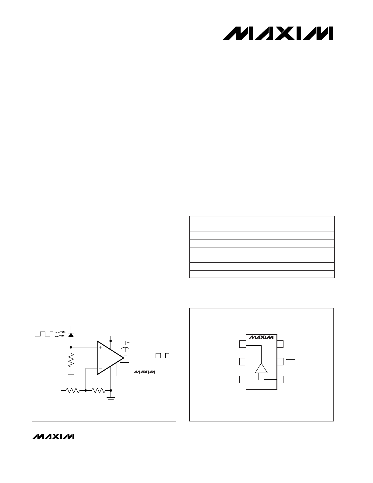
__________________Pin Configurations
V
CC
V
CC
V
CC
V
CC
R
D
SHDN
R1 R2
IR RECEIVER
OUT
0.1µF
MAX998
V
CC
GND
___________Typical Operating Circuit
19-1299; Rev 1; 1/98
PART
MAX976ESA
MAX976EUA
MAX978ESE
-40°C to +85°C
-40°C to +85°C
-40°C to +85°C
TEMP. RANGE PIN-PACKAGE
8 SO
8 µMAX
16 Narrow SO
_______________Ordering Information
Pin Configurations continued at end of data sheet
Rail-to-Rail is a registered trademark of Nippon Motorola Ltd.
MAX978EEE
MAX998ESA
MAX998EUT-T -40°C to +85°C
-40°C to +85°C
-40°C to +85°C 16 QSOP
8 SO
6 SOT23-6
SOT
TOP MARK
—
—
—
—
—
AAAO
Page 2
mV
MAX976/MAX978/MAX998
Single/Dual/Quad, SOT23, Single-Supply,
High-Speed, Low-Power Comparators
2 _______________________________________________________________________________________
ABSOLUTE MAXIMUM RATINGS
ELECTRICAL CHARACTERISTICS
(VCC= +2.7V to +5.5V, VCM= 0V, TA= -40°C to +85°C, unless otherwise noted. Typical values are at TA= +25°C.) (Note 1)
Stresses beyond those listed under “Absolute Maximum Ratings” may cause permanent damage to the device. These are stress ratings only, and functional
operation of the device at these or any other conditions beyond those indicated in the operational sections of the specifications is not implied. Exposure to
absolute maximum rating conditions for extended periods may affect device reliability.
Supply Voltage (VCC).............................................................+6V
SHDN (MAX998).........................................................-0.3V to 6V
All Other Pins..............................................-0.3V to (V
CC
+ 0.3V)
Duration of Output Short Circuit to GND or V
CC
........Continuous
Continuous Power Dissipation (T
A
= +70°C)
6-Pin SOT23-6 (derate 7.1mW/°C above +70°C) .........571mW
8-Pin µMAX (derate 4.10mW/°C above +70°C)............330mW
8-Pin SO (derate 5.88mW/°C above +70°C).................471mW
16-Pin Narrow SO (derate 8.70mW/°C above +70°C)..696mW
16-Pin QSOP (derate 8.33mW/°C above +70°C)..........667mW
Operating Temperature Range ..........................-40°C to +85°C
Storage Temperature Range.............................-65°C to +160°C
Lead Temperature (soldering, 10sec).............................+300°C
VCC= 5.5V
MAX998 only, SHDN = GND
I
SINK
= 2mA
VCC= 5.5V
Inferred from PSRR test
VCC= 5V (Note 4)
2.7V < VCC< 5.5V
CONDITIONS
mA
90
OUT Short-Circuit Current
74
I
SH
V0.1 0.4V
OL
OUT Output Voltage Low
nA±5 ±100I
OS
Input Offset Current
mVV
HYS
0.5 1.5 4
Input-Referred Hysteresis
nA1 500I
SD
Shutdown Supply Current
300 650
V2.7 5.5V
CC
Supply Voltage Range
dB63 100PSRRPower-Supply Rejection Ratio
UNITSMIN TYP MAXSYMBOLPARAMETER
C
LOAD
=10pF (Note 6) ns2t
SKEW
Propagation-Delay Skew
MAX976/MAX978 only ns1∆t
PD
Propagation-Delay Matching
Between Channels
Sinking
Sourcing
Overdrive = 50mV
ns
20 40
t
PD
Propagation Delay
I
SOURCE
= 2mA, VCC- V
OH
V0.1 0.4V
OH
OUT Output Voltage High
(Note 2) V-0.2 VCC- 1.2V
CMR
Common-Mode Voltage Range
-0.2V ≤ VCM≤ (VCC- 1.2V) dB66 95CMRRCommon-Mode Rejection Ratio
VCC= 5V (Note 3) mV
0.2 ±2
V
OS
Input Offset Voltage
TA= +25°C
TA= T
MIN
to T
MAX
±3
pFInput Capacitance 3C
IN
28
C
LOAD
=10pF,
VCC= 5V (Note 5)
Overdrive = 5mV
MAX998 only V
SHDN Input Voltage High
0.65 x V
CC
V
IH
MAX998 only V
SHDN Input Voltage Low
0.2 x V
CC
V
IL
MAX998 only, SHDN = GND,
V
OUT
= 0V to V
CC
nAOUT Leakage Current 1 200I
OUT
MAX998 only nA
SHDN Input Current
1 200I
SHDN
C
LOAD
=10pF ns1.6tR/t
F
Output Rise/Fall Time
MAX998 only, VCC= 5V, ICC= 10% of typical µs5t
SD
Shutdown Delay Time
VCC= 2.7V
µA
225
I
CC
Supply Current per Comparator
0.3 1.5 5
nAI
B
75 300Input Bias Current
All others
MAX976EUA, MAX998EUT
Page 3
MAX976/MAX978/MAX998
Single/Dual/Quad, SOT23, Single-Supply,
High-Speed, Low-Power Comparators
_______________________________________________________________________________________ 3
ELECTRICAL CHARACTERISTICS (continued)
(VCC= +2.7V to +5.5V, VCM= 0V, TA= -40°C to +85°C, unless otherwise noted. Typical values are at TA= +25°C.) (Note 1)
Note 1: The MAX998EUT specifications are 100% tested at T
A
= +25°C. Limits over the extended temperature range are guaran-
teed by design, not production tested.
Note 2: Inferred from CMRR test. Either input can be driven to the absolute maximum limit without false output inversion, as long as
the other input is within the common-mode voltage range.
Note 3: V
OS
is defined as the mean of trip points. The trip points are the extremities of the differential input voltage required to make
the comparator output change state (Figure 1).
Note 4: The difference between the upper and lower trip points is equal to the width of the input-referred hysteresis zone (Figure 1).
Note 5: Propagation Delay is guaranteed by design. For low overdrive conditions, V
TRIP
(Figure 1) is added to the overdrive.
Note 6: Propagation-Delay Skew is the difference between the positive-going and the negative-going propagation delay.
Note 7: For design purposes, the t
EN
can be as high as 60µs.
CONDITIONS
MAX998 only, VCC= 5V, ICC= 90% of typical
(Note 7)
µs15t
EN
Wake-Up from Shutdown
UNITSMIN TYP MAXSYMBOLPARAMETER
VCC= 0V to 5V step, output valid µs3t
PU
Power-Up Delay
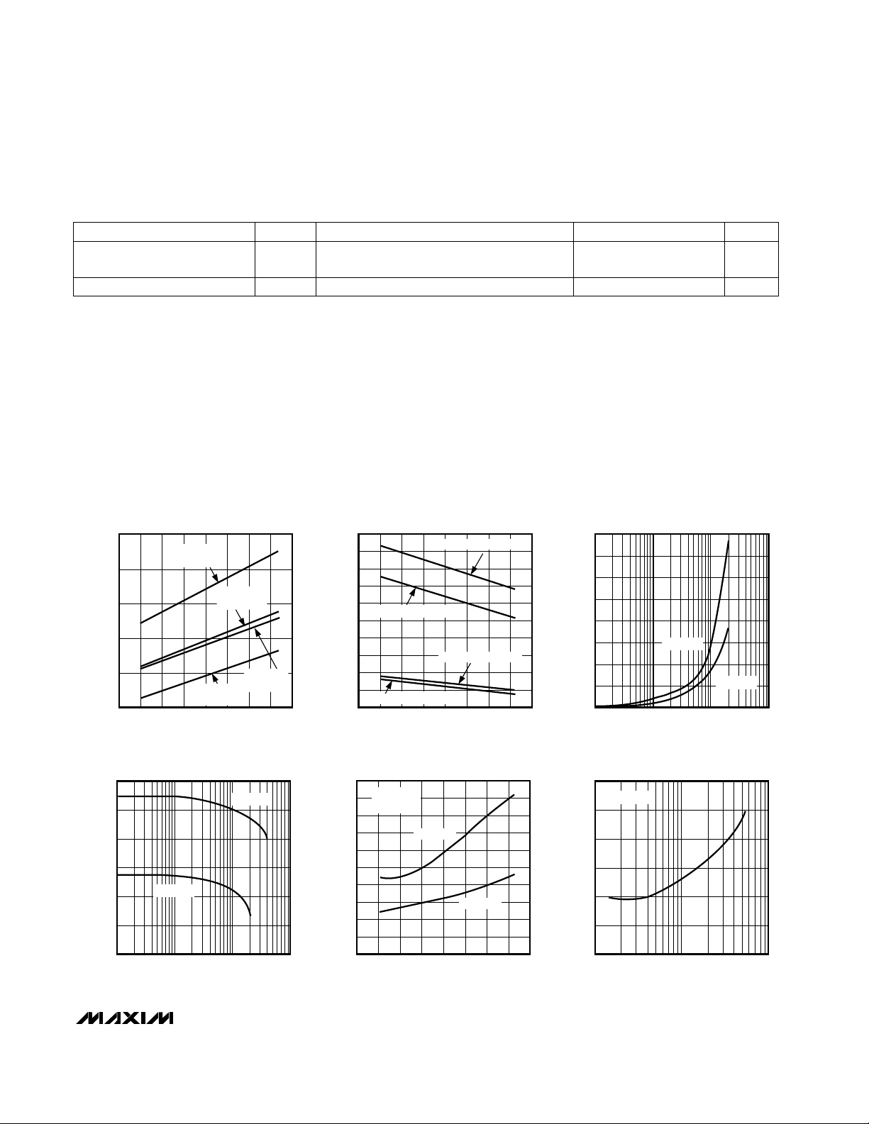
__________________________________________Typical Operating Characteristics
(VCC= +5V, VCM= 0V, TA= +25°C, unless otherwise noted.)
125
175
275
225
325
375
-60 -20 0-40 20 40 60 80 100
SUPPLY CURRENT PER COMPARATOR
vs. TEMPERATURE
MAX976 TOC01
TEMPERATURE (°C)
SUPPLY CURRENT PER COMPARATOR (µA)
VCC = 5.5V,
V
OUT
= LOW
VCC = 5.5V,
V
OUT
= HIGH
VCC = 2.7V,
V
OUT
= HIGH
VCC = 2.7V,
V
OUT
= LOW
10
30
20
50
40
70
60
80
100
90
110
-60 -20 0-40 20 40 60 80 100
SHORT-CIRCUIT OUTPUT CURRENT
vs. TEMPERATURE
MAZX976 TOC2
TEMPERATURE (°C)
OUTPUT CURRENT (mA)
VCC = 5.5V, SOURCING
VCC = 2.7V, SOURCING
VCC = 5.5V, SINKING
VCC = 2.7V, SINKING
1.6
0
0.1 1 10 100
OUTPUT LOW VOLTAGE vs.
OUTPUT SINK CURRENT
0.4
0.8
0.6
0.2
1.0
1.2
1.4
MAX976 TOC03
OUTPUT CURRENT (mA)
OUTPUT LOW VOLTAGE (V)
VCC = 5.5V
VCC = 2.7V
6
0
0.1 1 10 100
OUTPUT HIGH VOLTAGE vs.
OUTPUT SOURCE CURRENT
2
3
1
4
5
MAX976 TOC04
OUTPUT CURRENT (mA)
OUTPUT HIGH VOLTAGE (V)
VCC = 5.5V
VCC = 2.7V
17
19
18
21
20
22
24
23
25
26
27
-60 -20 0-40 20 40 60 80 100
PROPAGATION DELAY
vs. TEMPERATURE
MAZX976 TOC5
TEMPERATURE (°C)
PROPAGATION DELAY (ns)
VCC = 5.5V
VCC = 2.7V
VOD = 50mV
C
LOAD
= 15pF
40
10
10 100 1000
PROPAGATION DELAY
vs. CAPACITIVE LOAD
MAX976 TOC06
CAPACITIVE LOAD (pF)
PROPAGATION DELAY (ns)
15
25
20
30
35
VOD = 50mV
Page 4

V
IN+
50mV/div
10ns/div
PROPAGATION DELAY
(t
PD+, VCC
= 5V)
V
OUT
2V/div
MAX976 TOC13
VOD = 50mV
C
LOAD
= 15pF
10MHz RESPONSE
INPUT
50mV/div
20ns/div
OUTPUT
2V/div
V
OS
V
CC
GND
MAX976 TOC15
V
IN+
50mV/div
10ns/div
PROPAGATION DELAY
(t
PD-, VCC
= 5V)
V
OUT
2V/div
MAX976 TOC14
VOD = 50mV
C
LOAD
= 15pF
MAX976/MAX978/MAX998
Single/Dual/Quad, SOT23, Single-Supply,
High-Speed, Low-Power Comparators
4 _______________________________________________________________________________________
______________________________Typical Operating Characteristics (continued)
(VCC= +5V, VCM= 0V, TA= +25°C, unless otherwise noted.)
90
80
0
1 10 100
PROPAGATION DELAY
vs. INPUT OVERDRIVE
MAX976 TOC07
INPUT OVERDRIVE (mV)
PROPAGATION DELAY (ns)
10
30
20
50
40
70
60
C
LOAD
= 15pF
100
-1 2 3 4 50 1 6
INPUT BIAS CURRENT vs.
INPUT COMMON-MODE VOLTAGE
0.01
MAX976 TOC10
INPUT COMMON-MODE VOLTAGE (V)
INPUT BIAS CURRENT (nA)
0.1
1
10
VCC = 2.7V VCC = 5.5V
-2.0
-1.0
-1.5
0
-0.5
0.5
1.0
1.5
2.0
-60 -20 0-40 20 40 60 80 100
TRIP POINTS AND OFFSET VOLTAGE
vs. TEMPERATURE
MAX976 TOC08
TEMPERATURE (°C)
TRIP POINTS/OFFSET VOLTAGE (V)
V
TRIP+
V
TRIP-
V
OS
40
50
60
70
80
90
100
-60 -20-40 0 20 40 60 80 100
INPUT BIAS CURRENT
vs. TEMPERATURE
MAX976 TOC09
TEMPERATURE (°C)
INPUT BIAS CURRENT (nA)
VCC = 2.7V
VCC = 5.5V
V
IN+
50mV/div
10ns/div
PROPAGATION DELAY
(t
PD+, VCC
= 3V)
V
OUT
1V/div
MAX976 TOC11
VOD = 50mV
C
LOAD
= 15pF
V
IN+
50mV/div
10ns/div
PROPAGATION DELAY
(t
PD-, VCC
= 3V)
V
OUT
1V/div
MAX976 TOC12
C
LOAD
= 15pF
V
OD
= 50mV
Page 5

MAX976/MAX978/MAX998
Single/Dual/Quad, SOT23, Single-Supply,
High-Speed, Low-Power Comparators
_______________________________________________________________________________________
5
MAX978
33
MAX976
IN_+
24 IN_- Comparator Inverting Input2, 4, 6, 82, 4
42 GND
61 OUT_ Comparator Output
10, 11,
14, 15
6, 7
NAME
Ground9, 135
Comparator Noninverting Input1, 3, 5, 71, 3
76 V
CC
Supply Voltage, +2.7V to +5.5V12, 168
1, 5— N.C.
85
SHDN
Shutdown Input. Drive low for shutdown mode. Drive high or connect to VCCfor normal operation.
——
No Connection. Not internally connected.——
FUNCTION
MAX998
PIN
SOT23-6 SOSO/µMAX SO/QSOP
______________________________________________________________Pin Description
__________________Detailed Description
The MAX976/MAX978/MAX998 dual/quad/single comparators operate from a single +2.7V to +5.5V supply.
They achieve a 20ns propagation delay while consuming only 225µA of supply current per comparator. The
MAX998 features a low-power shutdown mode that
places the output in a high-impedance state and
reduces supply current to 1nA. Activate shutdown
mode by driving SHDN low.
The MAX976/MAX978/MAX998 comparator inputs have
a common-mode voltage range of -0.2V to (VCC- 1.2V).
Either input can be driven to the Absolute Maximum
Ratings limit without false output inversion, as long as
the other input is within the Common-Mode Voltage
Range. Their push/pull output structure is capable of
rail-to-rail operation without external pull-up circuitry,
making these devices ideal for interfacing with
CMOS/TTL logic. All inputs and outputs can tolerate a
continuous short-circuit fault condition to either supply.
The comparator’s internal hysteresis ensures clean output switching, even with slow-moving input signals.
______________________________Typical Operating Characteristics (continued)
(VCC= +5V, VCM= 0V, TA= +25°C, unless otherwise noted.)
SHDN
2V/div
200ns/div
SHUTDOWN DELAY TIME
V
OUT
2V/div
MAX976 TOC16
V
IN+
> V
IN-
SHDN
2V/div
5µs/div
WAKE-UP FROM SHUTDOWN
V
OUT
2V/div
MAX976 TOC17
V
IN+
> V
IN-
Page 6

Hysteresis
High-speed comparators can oscillate in the linear
operating region because of noise or undesired parasitic feedback. This tends to occur when the voltage on
one input is equal to or very close to the voltage on the
other input. The MAX976/MAX978/MAX998 have internal hysteresis to counter parasitic effects and noise.
The hysteresis in a comparator creates two trip points:
one for the rising input voltage and one for the falling
input voltage (Figure 1). The difference between the trip
points is the hysteresis. When the comparator input
voltages are equal, the hysteresis effectively causes
one comparator input voltage to move quickly past the
other, taking the input out of the region where oscillation occurs.
Figure 1 illustrates the case where IN- has a fixed voltage applied and IN+ is varied. If the inputs were
reversed, the figure would be the same, except with an
inverted output.
Input-Stage Circuitry
The MAX976/MAX978/MAX998 input common-mode
voltage range is from -0.2V to (VCC- 1.2V). The voltage
range for each comparator input extends to both V
CC
and GND. The output remains in the correct logic state
while one or both of the inputs are within the commonmode range. If both input levels are out of the commonmode range, input-stage current saturation occurs, and
the output becomes unpredictable.
Shutdown Mode
The MAX998 features a low-power shutdown mode,
which is activated by forcing SHDN low. Shutdown
mode reduces the supply current to 1nA (typical), disables the comparator, and places the output in a highimpedance state. Drive SHDN high to enable the
comparator. Do not leave SHDN unconnected. Since it
is a high-impedance input, leaving SHDN unconnected
could result in indeterminate logic levels, adversely
affecting comparator operation. Likewise, do not threestate SHDN. Due to the output leakage currents of
three-state devices and the small internal current for
SHDN, three-stating this pin could also result in indeterminate logic levels.
The maximum input voltage for SHDN is 6V, referred to
GND, and is not limited by V
CC
. This allows the use of
5V logic to drive SHDN while VCCoperates at a lower
voltage, such as 3V. The logic threshold limits for
SHDN are proportional to VCC(see
Electrical
Characteristics
).
_____________Applications Information
Circuit Layout and Bypassing
The MAX976/MAX978/MAX998 have a high-gain bandwidth and require careful board layout. We recommend
the following design guidelines:
1) Use a printed circuit board with an unbroken, low-
inductance ground plane. Surface-mount components are recommended.
2) Place a decoupling capacitor (a 0.1µF ceramic
capacitor is a good choice) between VCCand
ground as close to the pins as possible.
3) Keep lead lengths short on the inputs and outputs
to avoid unwanted parasitic feedback around the
comparators.
4) Solder the devices directly to the printed circuit
board instead of using a socket.
5) Minimize input impedance.
6) For slowly varying inputs, use a small capacitor
(~1000pF) across the inputs to improve stability.
Additional Hysteresis
Generate additional hysteresis with three resistors
using positive feedback, as shown in Figure 2. This
positive feedback method slows the hysteresis
response time. Calculate resistor values as follows:
1) Select R3. The leakage current of IN+ is typically
75nA, so the current through R3 should be at least
1.0µA to minimize errors caused by leakage current.
The current through R3 at the trip point is (V
REF
-
V
OUT
) / R3. Consider the two possible output states
when solving for R3. The two formulas are:
R3 = V
REF
/ 1.0µA
or
R3 = (VCC- V
REF
) / 1.0µA
Use the smaller of the two resulting resistor values.
For example, if V
REF
= 1.2V and VCC= 5.0V, the two
resistor values are 1.2MΩ and 3.8MΩ. Choose a
standard value for R3 of 1.2MΩ.
MAX976/MAX978/MAX998
Single/Dual/Quad, SOT23, Single-Supply,
High-Speed, Low-Power Comparators
6 _______________________________________________________________________________________
V
OL
V
OH
V
IN-
= 0
V
OS
=
V
TRIP+
+ V
TRIP-
2
COMPARATOR
OUTPUT
V
TRIP+
V
IN+
V
HYST
V
TRIP-
Figure 1. Input and Output Waveforms, Noninverting Input
Varied
Page 7

MAX976/MAX978/MAX998
Single/Dual/Quad, SOT23, Single-Supply,
High-Speed, Low-Power Comparators
_______________________________________________________________________________________ 7
2) Choose the hysteresis band required (VHB). For this
example, choose 100mV.
3) Calculate R1. R1 = R3 x (V
HB
/ VCC). Plugging in the
values for this example,
R1 = 1.2MΩ x (100mV / 5.0V) = 24kΩ
4) Choose the trip point for VINrising. This is the
threshold voltage at which the comparator switches
from low to high as VINrises above the trip point. In
this example, choose 3.0V.
5) Calculate R2 as follows:
Choose a standard value for R2 of 16kΩ.
6) Verify the trip voltage and hysteresis as follows:
IR Receiver
The
Typical Operating Circuit
shows an application using
the MAX998 as an infrared receiver. The infrared photodiode creates a current relative to the amount of infrared
light present. This current creates a voltage across RD.
When this voltage level crosses the voltage applied by the
voltage divider to the inverting input, the output transitions.
Window Comparator
The MAX976 is ideal for making a window detector
(undervoltage/overvoltage detector). The schematic
shown in Figure 3 uses a MAX6120 reference and component values selected for a 2.0V undervoltage threshold and a 2.5V overvoltage threshold. Choose different
thresholds by changing the values of R1, R2, and R3.
OUTA provides an active-low undervoltage indication,
and OUTB gives an active-low overvoltage indication.
ANDing the two outputs provides an active-high,
power-good signal. The design procedure is as follows:
1) Select R1. The leakage current into INB- is normally
75nA, so the current through R1 should exceed
1.0µA for the thresholds to be accurate. R1 values in
the 50kΩ to 100kΩ range are typical.
2) Choose the overvoltage threshold (V
OTH
) when V
IN
is rising, and calculate R2 and R3 with the following
formula:
R
SUM
= R2 + R3 = R1 x [V
OTH
/ (V
REF
+ VH) - 1]
where VH= 1/2V
HYST
.
3) Choose the undervoltage threshold (V
UTH
) when V
IN
is falling, and calculate R2 with the following formula:
R2 = (R1 + R
SUM
) x [(V
REF
- VH) / V
UTH
] - R1
where VH= 1/2V
HYST
.
4) Calculate R3 with the following formula:
R3 = (R
SUM
) - R2
5) Verify the resistor values. The equations are as follows:
V
OTH
= (V
REF
+ VH) x (R1 + R2 + R3) / R1
V
UTH
= (V
REF
- VH) x (R1 + R2 + R3) / (R1 + R2)
V rising: V = V x R1 x
1
R1
V falling
IN THR REF
IN
:
+ +
= −
= −
1
2
1
3
1
3
R R
V V
R x V
R
Hysteresis V V
THF THR
CC
THR THF
R2 =
1
V
V x R1
1
R1
1
R3
R2 =
1
3.0V
1.2 x 24k
1
24k
1
1.2M
16.2k
THR
REF
− −
− −
=
Ω Ω
Ω
V
CC
MAX976
MAX978
MAX998
OUT
0.1µF
R3
R1
R2
V
REF
GND
V
IN
V
CC
Figure 2. Additional Hysteresis
3
1
3
4
R3
82.1k, 1%
V
CC
V
IN
R2
24.9k,
1%
R1
100k,
1%
2
6
OVERVOLTAGE
UNDERVOLTAGE
POWER GOOD
1/2
MAX976
MAX6120
1
2
V
CC
8
7
5
0.1µF
1/2
MAX976
Figure 3. Window Comparator
Page 8

MAX976/MAX978/MAX998
Single/Dual/Quad, SOT23, Single-Supply,
High-Speed, Low-Power Comparators
Maxim cannot assume responsibility for use of any circuitry other than circuitry entirely embodied in a Maxim product. No circuit patent licenses are
implied. Maxim reserves the right to change the circuitry and specifications without notice at any time.
8
_____________________Maxim Integrated Products, 120 San Gabriel Drive, Sunnyvale, CA 94086 408-737-7600
© 1998 Maxim Integrated Products Printed USA is a registered trademark of Maxim Integrated Products.
______________________________________________Pin Configurations (continued)
MAX976
TOP VIEW
+
+
-
16
15
14
13
12
11
10
9
1
2
3
4
5
6
7
8
INA+ V
CC
OUTA
OUTB
GND
V
CC
OUTC
OUTD
GND
SO/QSOP
INA-
INB+
INC-
INB-
INC+
IND+
IND-
MAX978
+
+
-
+
+
-
OUT
N.C.GND
1
2
87SHDN
V
CC
IN-
IN+
N.C.
SO
3
4
6
5
MAX998
-
+
OUTB
GNDINB-
1
2
87V
CC
OUTAINA-
INB+
INA+
SO/µMAX
3
4
6
5
___________________Chip Information
TRANSISTOR COUNT: 415 (MAX976)
830 (MAX978)
300 (MAX998)
________________________________________________________Package Information
6LSOT.EPS
 Loading...