

Page 1
General Description
The MAX9943/MAX9944 is a family of high-voltage
amplifiers that offers precision, low drift, and low-power
consumption.
The MAX9943 (single) and MAX9944 (dual) op amps
offer 2.4MHz of gain-bandwidth product with only
550µA of supply current per amplifier.
The MAX9943/MAX9944 family has a wide power supply range operating from ±3V to ±19V dual supplies or
a 6V to 38V single supply.
The MAX9943/MAX9944 is ideal for sensor signal conditioning, high-performance industrial instrumentation and
loop-powered systems (e.g., 4mA–20mA transmitters).
The MAX9943 is offered in a space-saving 6-pin TDFN or
8-pin µMAX
®
package. The MAX9944 is offered in an
8-pin SO or an 8-pin TDFN package. These devices are
specified over the -40°C to +125°C automotive temperature range.
Applications
Sensor Interfaces
Loop-Powered Systems
Industrial Instrumentation
High-Voltage ATE
High-Performance ADC/DAC Input/Output
Amplifiers
Features
♦ Wide 6V to 38V Supply Range
♦ Low 100µV (max) Input Offset Voltage
♦ Low 0.4µV/°C Offset Drift
♦ Unity Gain Stable with 1nF Load Capacitance
♦ 2.4MHz Gain-Bandwidth Product
♦ 550µA Supply Current
♦ 20mA Output Current
♦ Package Options
3mm x 5mm, 8-Pin µMAX or 3mm x 3mm, 6-Pin
TDFN Packages (Single)
5mm x 6mm, 8-Pin SO or 3mm x 3mm, 8-Pin
TDFN Packages (Dual)
MAX9943/MAX9944
High-Voltage, Precision, Low-Power Op Amps
________________________________________________________________
Maxim Integrated Products
1
19-4433; Rev 1; 4/09
For pricing, delivery, and ordering information, please contact Maxim Direct at 1-888-629-4642,
or visit Maxim’s website at www.maxim-ic.com.
Package Detail
Ordering Information
+
Denotes a lead(Pb)-free/RoHS-compliant package.
*
EP = Exposed pad.
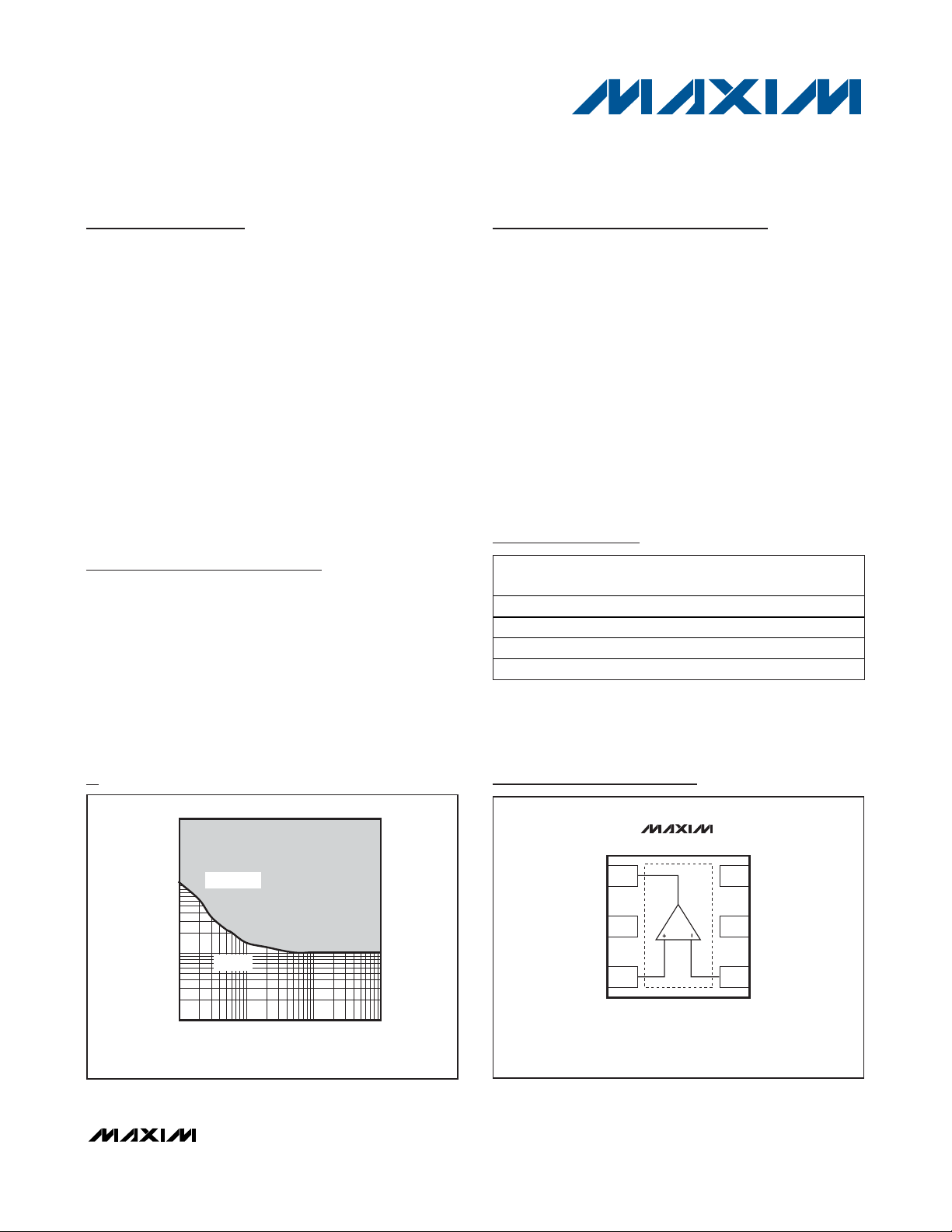
Capacitive Load vs. Resistive Load
µMAX is a registered trademark of Maxim Integrated Products, Inc.
Pin Configurations appear at end of data sheet.
PART TEMP RANGE
MAX9943AUA+ -40°C to +125°C 8 µMAX AACA
MAX9943ATT+ -40°C to +125°C 6 TDFN-EP* AUF
MAX9944ASA+ -40°C to +125°C 8 SO —
MAX9944ATA+ -40°C to +125°C 8 TDFN-EP* BLN
PINPACKAGE
MARK
TOP
100,000
MAX9943 toc17
10,000
(pF)
LOAD
C
1000
100
UNSTABLE
STABLE
100 100,000
1000 10,000
R
(Ω)
LOAD
TOP VIEW
1
OUT
2
V
EE
3
IN+
6 TDFN-EP
*EP = EXPOSED PAD.
MAX9943
*EP
TOP VIEW
V
6
CC
5
N.C.
4
IN-
Page 2
MAX9943/MAX9944
High-Voltage, Precision, Low-Power Op Amps
2 _______________________________________________________________________________________
ABSOLUTE MAXIMUM RATINGS
Stresses beyond those listed under “Absolute Maximum Ratings” may cause permanent damage to the device. These are stress ratings only, and functional
operation of the device at these or any other conditions beyond those indicated in the operational sections of the specifications is not implied. Exposure to
absolute maximum rating conditions for extended periods may affect device reliability.
Supply Voltage (VCCto VEE) ..................................-0.3V to +40V
All Other Pins (Note 1) .....................(V
EE
- 0.3V) to (VCC+ 0.3V)
OUT Short-Circuit Current Duration
8-Pin µMAX (V
CC
- VEE≤ 20V)...............................................3s
8-Pin µMAX (V
CC
- VEE> 20V) ................................Momentary
6-Pin TDFN (V
CC
- VEE≤ 20V) .............................................60s
6-Pin TDFN (V
CC
- VEE> 20V)...............................................2s
8-Pin SO (V
CC
- VEE≤ 20V) .................................................60s
8-Pin SO (V
CC
- VEE> 20V)...................................................2s
8-Pin TDFN (V
CC
- VEE≤ 20V) .............................................60s
8-Pin TDFN (V
CC
- VEE> 20V)...............................................2s
Continuous Input Current (Any Pins) ................................±20mA
Thermal Limits (Note 2)
Multiple Layer PCB
Continuous Power Dissipation (T
A
= +70°C)
8-Pin µMAX (derate 4.8mW/°C above +70°C) ...........387.8mW
θ
JA
.........................................................................206.3°C/W
θ
JC
..............................................................................42°C/W
6-Pin TDFN-EP (derate 23.8mW/°C above +70°C)..1904.8mW
θ
JA
..............................................................................42°C/W
θ
JC
................................................................................9°C/W
8-Pin SO (derate 7.6mW/°C above +70°C)...................606.1W
θ
JA
............................................................................132°C/W
θ
JC
..............................................................................38°C/W
8-Pin TDFN-EP (derate 24.4mW/°C above +70°C)..1951.2mW
θ
JA
..............................................................................41°C/W
θ
JC
................................................................................8°C/W
Operating Temperature Range .........................-40°C to +125°C
Junction Temperature......................................................+150°C
Lead Temperature (soldering, 10s) .................................+300°C
ELECTRICAL CHARACTERISTICS
(VCC= 15V, VEE= -15V, VCM= 0, RL= 10kΩ to GND, GND = 0, TA= -40°C to +125°C. Typical values are at TA= +25°C, unless otherwise noted.) (Note 3)
Note 1: Operation is limited by thermal limits.
Note 2: Package thermal resistances were obtained using the method described in JEDEC specification JESD51-7, using a four-
layer board. For detailed information on package thermal considerations, refer to www.maxim-ic.com/thermal-tutorial
.
PARAMETER SYMBOL CONDITIONS MIN TYP MAX UNITS
DC CHARACTERISTICS
Operating Supply Voltage Range V
Quiescent Supply Current per
Amplifier
SUPPLY
I
CC
Power-Supply Rejection Ratio PSRR VS = ±3V to ±19V 105 130 dB
Input Offset Voltage V
Input Offset Voltage Drift TCV
Input Bias Current I
Input Offset Current I
Input Voltage Range V
IN+
OS
OS
BIAS
OS
, V
Common-Mode Rejection Ratio CMRR
Guaranteed by PSRR test ±3 ±19 V
550 950 µA
TA = +25°C 20 100
TA = -40°C to +125°C 240
0.4 µV/°C
VEE + 0.3V ≤ VCM ≤ VCC - 1.8V 4 20
VEE ≤ VCM ≤ VCC - 1.8V 90
VEE ≤ VCM ≤ VCC - 1.8V 1 10 nA
Guaranteed by CMRR test,
IN-
T
= -40°C to +125°C
A
V
EE
VEE + 0.3V ≤ VCM ≤ VCC - 1.8V 105 125
≤ VCM ≤ VCC - 1.8V 105
V
EE
VCC -
1.8
µV
nA
V
dB
Page 3
MAX9943/MAX9944
High-Voltage, Precision, Low-Power Op Amps
_______________________________________________________________________________________ 3
ELECTRICAL CHARACTERISTICS (continued)
(VCC= 15V, VEE= -15V, VCM= 0, RL= 10kΩ to GND, GND = 0, TA= -40°C to +125°C. Typical values are at TA= +25°C, unless otherwise noted.) (Note 3)
Note 3: All devices are 100% production tested at T
A
= +25°C. Temperature limits are guaranteed by design.
PARAMETER SYMBOL CONDITIONS MIN TYP MAX UNITS
-13.5V ≤ VO ≤ +13.5V, RL = 10kΩ,
T
= +25°C
A
-13.5V ≤ VO ≤ +13.5V, RL = 10kΩ,
T
= -40°C to +125°C
Open-Loop Gain A
VOL
A
-12V ≤ V
T
A
-12V ≤ V
T
A
≤ +12V, R
O
= +25°C
≤ +12V, R
O
= -40°C to +85°C
= 600Ω,
L
= 600Ω,
L
RL = 10kΩ
V
OH
RL = 600Ω
Output Voltage Swing
TA = +25°C
T
= -40°C to +85°CVCC - 2
A
RL = 10kΩ
V
OL
TA = +25°C
RL = 600Ω
T
= -40°C to +85°C
A
Short-Circuit Current I
SC
TA = +25°C60
TA = -40°C to +125°C 100
AC CHARACTERISTICS
Gain Bandwidth Product GBWP 2.4 MHz
Slew Rate SR -5V ≤ V
Input Voltage Noise Density e
n
f = 1kHz 17.6 nV/√Hz
≤ +5V 0.35 V/µs
OUT
Input Voltage Noise TOTAL NOISE 0.1Hz ≤ f ≤ 10Hz 500 nV
Input Current Noise Density I
Capacitive Loading C
n
LOAD
f = 1kHz 0.18 pA/√Hz
No sustained oscillation 1000 pF
115 130
100
100 110
90
-
V
CC
0.2
V
-
CC
1.8
dB
V
+
EE
V
0.1
V
+
EE
1
V
+
EE
1.1
mA
Page 4
MAX9943/MAX9944
High-Voltage, Precision, Low-Power Op Amps
4 _______________________________________________________________________________________
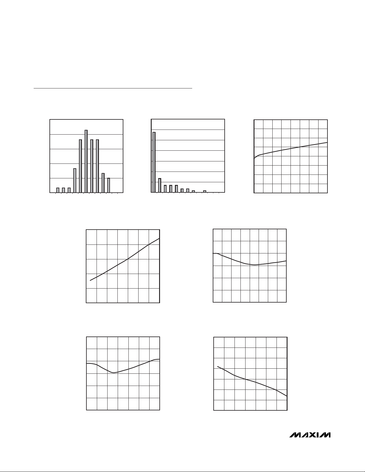
Typical Operating Characteristics
(VCC= 15V, VEE= -15V, VCM= 0, RL= 10kΩ to GND, GND = 0, TA= +25°C, unless otherwise noted.)
OFFSET VOLTAGE HISTOGRAM
25
20
15
10
FREQUENCY (%)
5
0
-60 -40 -30-50 -20 -10
OFFSET VOLTAGE (µV)
2010 30 40 50 60
0
MAX9943 toc01
FREQUENCY (%)
SUPPLY CURRENT vs. TEMPERATURE
800
700
600
500
SUPPLY CURRENT (µA)
400
70
60
50
40
30
20
10
0
INPUT VOLTAGE OFFSET
DRIFT HISTOGRAM
-0.3 -0.2
-0.25
-0.1
-0.15
VOS DRIFT (µV/°C)
MAX9943 toc04
-0.05
SUPPLY CURRENT vs. SUPPLY VOLTAGE
700
650
MAX9943 toc02
600
550
500
450
SUPPLY CURRENT (µA)
400
350
0.1
0
0.05
0.15
0.2
0.3
0.25
300
6141810 22 26 30 34 38
SUPPLY VOLTAGE (V)
MAX9943 toc03
OFFSET VOLTAGE vs. SUPPLY VOLTAGE
30
25
20
15
10
OFFSET VOLTAGE (µV)
5
MAX9943 toc05
300
-50 0-25 25 50 75 100 125
TEMPERATURE (°C)
0
61410 18 22 26 30 34 38
SUPPLY VOLTAGE (V)
OFFSET VOLTAGE
vs. COMMON-MODE VOLTAGE
30
25
20
15
10
OFFSET VOLTAGE (µV)
5
0
-14 -2 2-10 -6 6 10 14
COMMON-MODE VOLTAGE (V)
MAX9943 toc06
OFFSET VOLTAGE vs. TEMPERATURE
100
80
60
40
20
OFFSET VOLTAGE (µV)
0
-20
-40
-50 0 25-25 50 75 100 125
TEMPERATURE (°C)
MAX9943 toc07
Page 5
VOL vs. OUTPUT CURRENT
MAX9943 toc13
OUTPUT VOLTAGE (V)
010515202530
-16
-15
-14
-13
-12
TA = +85°C
TA = +125°C
TA = -40°C
TA = +25°C
OUTPUT CURRENT (mA)
MAX9943/MAX9944
High-Voltage, Precision, Low-Power Op Amps
_______________________________________________________________________________________ 5
Typical Operating Characteristics (continued)
(VCC= 15V, VEE= -15V, VCM= 0, RL= 10kΩ to GND, GND = 0, TA= +25°C, unless otherwise noted.)
INPUT BIAS CURRENT
vs. COMMON-MODE VOLTAGE
3.0
2.5
2.0
1.5
1.0
INPUT BIAS CURRENT (nA)
0.5
0
-14 -2 2-10 -6 6 10 14
COMMON-MODE VOLTAGE (V)
COMMON-MODE REJECTION
RATIO vs. FREQUENCY
140
130
120
110
100
CMRR (dB)
90
80
70
60
0.001 10,000
FREQUENCY (kHz)
3.0
MAX9943 toc08
MAX9943 toc10
10001000.01 0.1 1 10
2.5
2.0
1.5
1.0
INPUT BIAS CURRENT (nA)
0.5
0
160
140
120
100
80
PSRR (dB)
60
40
20
0
0.001 10,000
INPUT BIAS CURRENT
vs. SUPPLY VOLTAGE
61410 18 22 26 30 34 38
SUPPLY VOLTAGE (V)
POWER-SUPPLY REJECTION
RATIO vs. FREQUENCY
FREQUENCY (kHz)
MAX9943 toc09
MAX9943 toc11
10001000.01 0.1 1 10
16
15
14
OUTPUT VOLTAGE (V)
13
12
010515202530
TA = -40°C
TA = +85°C
TA = +125°C
OUTPUT CURRENT (mA)
TA = +25°C
MAX9943 toc12
VOH vs. OUTPUT CURRENT
Page 6

MAX9943/MAX9944
High-Voltage, Precision, Low-Power Op Amps
6 _______________________________________________________________________________________
Typical Operating Characteristics (continued)
(VCC= 15V, VEE= -15V, VCM= 0, RL= 10kΩ to GND, GND = 0, TA= +25°C, unless otherwise noted.)
OUTPUT IMPEDANCE vs. FREQUENCY
MAX9943 toc14
FREQUENCY (kHz)
OUTPUT IMPEDANCE (Ω)
1000100101
0.1
1
10
100
1000
0.01
0.1 10,000
INPUT VOLTAGE NOISE
vs. FREQUENCY
MAX9943 toc15
10,000100010010
FREQUENCY (Hz)
100
90
80
70
60
50
40
30
20
INPUT VOLTAGE NOISE (nV/√Hz)
10
0
1 100,000
OPEN-LOOP GAIN vs. FREQUENCY
140
120
100
80
60
40
OPEN-LOOP GAIN (dB)
20
0
-20
0.001
0.00001 1000
0.0001
0.01
FREQUENCY (kHz)
10
0.1
1
SMALL SIGNAL-STEP RESPONSE
100
10,000
MAX9943 toc18
MAX9943 toc16
20mV/div
CAPACITIVE LOAD vs. RESISTIVE LOAD
100,000
10,000
(pF)
LOAD
C
1000
100
UNSTABLE
STABLE
100 100,000
1000 10,000
R
(Ω)
LOAD
LARGE SIGNAL-STEP RESPONSE
MAX9943 toc17
MAX9943 toc19
1V/div
OUT
1µs/div
OUT
10µs/div
Page 7
Detailed Description
The MAX9943/MAX9944 are single/dual operational
amplifiers designed for industrial applications. They
operate from 6V to 38V supply range while maintaining
excellent performance. These devices utilize a threestage architecture optimized for low offset voltage and
low input noise with only 550µA supply current. The
devices are unity gain stable with a 1nF capacitive
load. These well-matched devices guarantee the high
open-loop gain, CMRR, PSRR, and low voltage offset.
The MAX9943/MAX9944 provide a wide input/output
voltage range. The input terminals of the MAX9943/
MAX9944 are protected from excessive differential voltage with back-to-back diodes. The input signal current
is also limited by an internal series resistor. With a 40V
differential voltage, the input current is limited to 20mA.
The output can swing to the negative rail while delivering 20mA of current, which is ideal for loop-powered
system applications. The specifications and operation
of the MAX9943/MAX9944 family is guaranteed over the
-40°C to +125°C temperature range.
Application Information
Bias Current vs. Input Common Mode
The MAX9943/MAX9944 use an internal bias current
cancellation circuit to achieve very low bias current
over a wide input common-mode range. For such a circuit to function properly, the input common mode must
be at least 300mV away from the negative supply VEE.
The input common mode can reach the negative supply VEE. However, in the region between VEEand VEE+
0.3V, there is an increase in bias current for both
inputs.
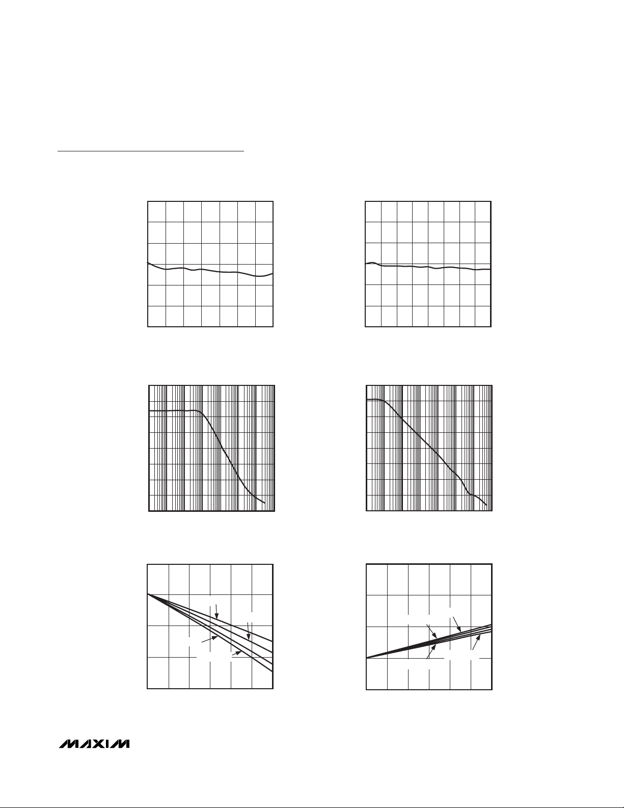
Capacitive Load Stability
Driving large capacitive loads can cause instability in
many op amps. The MAX9943/MAX9944 are stable with
capacitive loads up to 1nF. The Capacitive Load vs.
Resistive Load graph in the
Typical Operating
Characteristics
gives the stable operation region for
capacitive versus resistive loads. Stability with higher
capacitive loads can be improved by adding an isolation resistor in series with the op-amp output, as shown
in Figure 1. This resistor improves the circuit’s phase
MAX9943/MAX9944
High-Voltage, Precision, Low-Power Op Amps
_______________________________________________________________________________________ 7
Pin Description
MAX9943
6 TDFN-EP
1 6 — OUT Output
— — 1 OUTA Output A
— — 7 OUTB Output B
24 4 V
3 3 — IN+ Positive Input
— — 3 INA+ Positive Input A
— — 5 INB+ Positive Input B
4 2 — IN- Negative Input
— — 2 INA- Negative Input A
— — 6 INB- Negative Input B
5 1, 5, 8 — N.C. No Connection
67 8 V
—— — EP
MAX9943
8 µMAX
MAX9944
8 SO/TDFN-EP
NAME FUNCTION
Negative Power Supply. Bypass with a 0.1µF capacitor to ground.
EE
Positive Power Supply. Bypass with a 0.1µF capacitor to ground.
CC
Exposed Pad (TDFN Only). Connect to a large ground plane to
maximize thermal performance. Not intended as an electrical
connection point.
Page 8

MAX9943/MAX9944
margin by isolating the load capacitor from the amplifier’s output.
Power Supplies and Layout
The MAX9943/MAX9944 can operate with dual supplies
from ±3V to ±19V or with a single supply from +6V to
+38V with respect to ground. When used with dual supplies, bypass both VCCand VEEwith their own 0.1µF
capacitor to ground. When used with a single supply,
bypass VCCwith a 0.1µF capacitor to ground. Careful
layout technique helps optimize performance by
decreasing the amount of stray capacitance at the op
amp’s inputs and outputs. To decrease stray capacitance, minimize trace lengths by placing external components close to the op amp’s pins.
Output Current Capability
The MAX9943/MAX9944 are capable of driving heavy
loads such as the ones that can be found in loop-powered systems for remote sensors. The information is
transmitted through ±20mA or 4mA–20mA current output
across long lines that are terminated with low resistance
loads (e.g., 600Ω). The
Typical Application Circuit
shows
the MAX9944 used as a voltage-to-current converter with
a current-sense amplifier in the feedback loop. Because
of the high output current capability of the MAX9944, the
device can be used to directly drive the current-loop.
The specifications and operation of the MAX9943/
MAX9944 family is guaranteed over the -40°C to
+125°C temperature range, However, when used in
applications with ±15V supply voltage (see Figure 3),
the capability of driving more than ±20mA of current is
limited to the -40°C to +85°C temperature range. Use a
lower supply voltage if this current must be delivered at
a higher temperature range.
Input Common Mode and Output Swing
The MAX9943/MAX9944 input common-mode range
can swing to the negative rail VEE. The output voltage
can also swing to the negative rail VEEif the output
stage is not heavily loaded. These two features are very
important for applications where the MAX9943/
MAX9944 are used with a single-supply (VEEconnected to ground). One of the applications that can benefit
from these features is when the single-supply op amp is
driving an ADC.
Input Differential Voltage Protection
During normal op-amp operation, the inverting and noninverting inputs of the MAX9943/MAX9944 are at essentially the same voltage. However, either due to fast
input voltage transients or due to other fault conditions,
these pins can be forced to be at two different voltages.
Internal back-to-back diodes and series resistors protect the inputs from an excessive differential voltage
(see Figure 2). Therefore, IN+ and IN- can be any voltage within the range shown in the absolute maximum
rating. Note the protection time is still dependent on the
package thermal limits.
Chip Information
PROCESS: BiCMOS
High-Voltage, Precision, Low-Power Op Amps
8 _______________________________________________________________________________________
Figure 1. Capacitive Load Driving Circuit
Figure 2. Input Protection Circuit
R
ISO
MAX9943
INPUT
1.5kΩ
1.5kΩ
OUTPUT
C
L
Page 9

MAX9943/MAX9944
High-Voltage, Precision, Low-Power Op Amps
_______________________________________________________________________________________ 9
Figure 3. Typical ±20mA Current-Source in Loop-Powered Systems
+15V
-15V
DAC
MAX9944
-15V
V
REF
R
SENSE
R
LOAD
Page 10

MAX9943/MAX9944
High-Voltage, Precision, Low-Power Op Amps
10 ______________________________________________________________________________________
Pin Configurations
TOP VIEW
MAX9944
+
V
8
CC
N.C.
MAX9943
+
1
87N.C.
OUTA
1
2IN-
IN+
3
4
V
EE
8 µMAX
TOP VIEW
OUT
V
EE
IN+
MAX9943
1
2
3
*EP
TOP VIEW
6 TDFN
NOT TO SCALE.
*EP = EXPOSED PAD.
OUTB
7
INB-
6
5
INB+
INA+
V
2INA-
3
4
EE
V
CC
OUT
6
N.C.
5
8 SO
MAX9944
V
6
CC
5
N.C.
4
IN-
OUTA
INA+
V
+
1
2INA-
3
4
EE
*EP
V
8
CC
OUTB
7
INB-
6
INB+
5
TOP VIEW
8 TDFN
Page 11
MAX9943/MAX9944
PACKAGE TYPE PACKAGE CODE DOCUMENT NO.
8 µMAX U8+1
21-0036
6 TDFN-EP T633+2
21-0137
8 SO S8+4
21-0041
8 TDFN-EP T833+2
21-0137
Package Information
For the latest package outline information and land patterns, go to www.maxim-ic.com/packages.
High-Voltage, Precision, Low-Power Op Amps
______________________________________________________________________________________ 11
α
8LUMAXD.EPS
α
Page 12

MAX9943/MAX9944
High-Voltage, Precision, Low-Power Op Amps
12 ______________________________________________________________________________________
Package Information (continued)
For the latest package outline information and land patterns, go to www.maxim-ic.com/packages.
6, 8, &10L, DFN THIN.EPS
Page 13

MAX9943/MAX9944
High-Voltage, Precision, Low-Power Op Amps
______________________________________________________________________________________ 13
Package Information (continued)
For the latest package outline information and land patterns, go to www.maxim-ic.com/packages.
COMMON DIMENSIONS
SYMBOL MIN. MAX.
A 0.70 0.80
D 2.90 3.10
E 2.90 3.10
0.00 0.05
A1
L 0.20 0.40
0.25 MIN.k
A2 0.20 REF.
PACKAGE VARIATIONS
PKG. CODE N D2 E2 e JEDEC SPEC b
T633-2 6 1.50±0.10 2.30±0.10 0.95 BSC MO229 / WEEA 0.40±0.05 1.90 REF
T833-2 8 1.50±0.10 2.30±0.10 0.65 BSC MO229 / WEEC 0.30±0.05 1.95 REF
T833-3 8 1.50±0.10 2.30±0.10 0.65 BSC MO229 / WEEC 0.30±0.05 1.95 REF
1.50±0.10 MO229 / WEED-3
2.30±0.10 MO229 / WEED-3 2.00 REF0.25±0.050.50 BSC1.50±0.1010T1033-2
0.40 BSC - - - - 0.20±0.05 2.40 REFT1433-2 14 2.30±0.101.70±0.10
[(N/2)-1] x e
2.00 REF0.25±0.050.50 BSC2.30±0.1010T1033-1
2.40 REF0.20±0.05- - - - 0.40 BSC1.70±0.10 2.30±0.1014T1433-1
Page 14
MAX9943/MAX9944
High-Voltage, Precision, Low-Power Op Amps
14 ______________________________________________________________________________________
Package Information (continued)
For the latest package outline information and land patterns, go to www.maxim-ic.com/packages.
N
HE
1
TOP VIEW
D
A
e
FRONT VIEW
B
A1
INCHES
DIM
MIN
0.053A
0.004
A1
0.014
B
0.007
C
e 0.050 BSC 1.27 BSC
0.150
E
H 0.2440.228 5.80 6.20
0.016L
VARIATIONS:
INCHES
MINDIM
D
0.189 0.197 AA5.004.80 8
0.337 0.344 AB8.758.55 14
D
C
L
0\-8\
MAX
0.069
0.010
0.019
0.010
0.157
0.050
MAX
0.3940.386D
MILLIMETERS
MAX
MIN
1.35
1.75
0.10
0.25
0.35
0.49
0.19
0.25
3.80 4.00
0.40 1.27
MILLIMETERS
MAX
MIN
9.80 10.00
N MS012
16
AC
SOICN .EPS
SIDE VIEW
PROPRIETARY INFORMATION
TITLE:
PACKAGE OUTLINE, .150" SOIC
APPROVAL
21-0041
REV.DOCUMENT CONTROL NO.
1
B
1
Page 15

MAX9943/MAX9944
High-Voltage, Precision, Low-Power Op Amps
Maxim cannot assume responsibility for use of any circuitry other than circuitry entirely embodied in a Maxim product. No circuit patent licenses are
implied. Maxim reserves the right to change the circuitry and specifications without notice at any time.
Maxim Integrated Products, 120 San Gabriel Drive, Sunnyvale, CA 94086 408-737-7600 ____________________
15
© 2009 Maxim Integrated Products Maxim is a registered trademark of Maxim Integrated Products, Inc.
Revision History
REVISION
NUMBER
0 3/09 Initial release —
1 4/09 Removed future product reference for the MAX9944, updated EC table 1, 2
REVISION
DATE
DESCRIPTION
PAGES
CHANGED
 Loading...