

Page 1
19-4233; Rev 0; 8/08
Automotive Current-Sense Amplifier
with Reverse-Battery Protection
General Description
The MAX9937 is a tiny automotive grade current-sense
amplifier designed for unidirectional high-side currentsense applications. This device addresses major areas
of concern for automotive applications including loaddump protection up to +40V, reverse-battery protection, and filtering for EMI and transient performance.
The MAX9937 also features a low input offset voltage of
±1.2mV (max) at +25°C with a low temperature drift of
just 1µV/°C (typ).
The MAX9937 is available in a 5-pin SC70 package and
is rated over the -40°C to +125°C temperature range.
Applications
Automotive Battery Current Sense
Fuse Box Current Sense
ECU Current Monitor
Pin Configuration appears at end of data sheet.
Features
♦ Reverse Battery and Load-Dump Protection
-20V to +40V
♦ +4V to +28V Input Common-Mode Range
♦ Flexible EMI Filtering
♦ Low V
♦ Low V
: ±1.2mV (max)
OS
Drift: 1µV/°C (typ)
OS
♦ 20µA Supply Current
♦ 350kHz, 3dB Small Signal Bandwidth
Ordering Information
PART TEMP RANGE
MAX9937AXK+T -40°C to +125°C 5 SC70 +ATB
+
Denotes a lead-free/RoHS-compliant package.
T = Tape and reel.
PIN-
PACKAGE
MARK
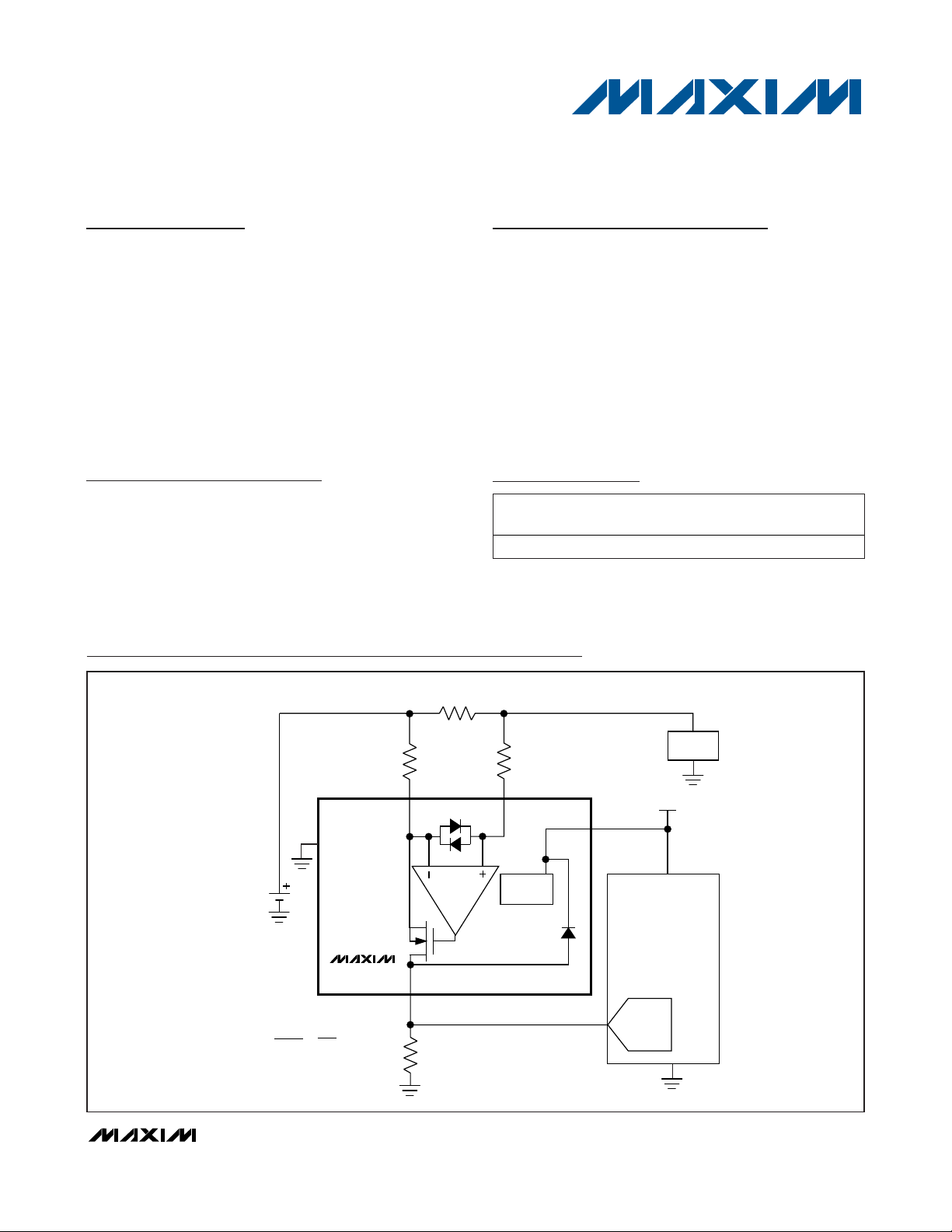
Typical Application Circuit
MAX9937
TOP
R
SENSE
RS+
R
RSP
499Ω
RSP
GND
V
= 4V
BAT
TO 28V
MAX9937
R
V
OUT
OUT
V
SENSE
=
R
RSP
GAIN =
________________________________________________________________
R
OUT
10kΩ
OUT
RS-
R
RSN
499Ω
RSN
BIAS
BLOCK
V
CC
MICROCONTROLLER
ADC
LOAD
5V
Maxim Integrated Products
1
For pricing, delivery, and ordering information, please contact Maxim Direct at 1-888-629-4642,
or visit Maxim’s website at www.maxim-ic.com.
Page 2
MAX9937
Automotive Current-Sense Amplifier
with Reverse-Battery Protection
2 _______________________________________________________________________________________
ABSOLUTE MAXIMUM RATINGS
ELECTRICAL CHARACTERISTICS
(VCC= 5V, V
BAT
= V
RS+
= 12V, V
SENSE
= (V
RS+
- V
RS-
) = 0, R
RSP
= R
RSN
= 500Ω, R
OUT
= 10kΩ, TA= -40°C to +125°C. Typical
values are at T
A
= +25°C, unless otherwise noted. See the
Typical Application Circuit
.) (Note 2)
Stresses beyond those listed under “Absolute Maximum Ratings” may cause permanent damage to the device. These are stress ratings only, and functional
operation of the device at these or any other conditions beyond those indicated in the operational sections of the specifications is not implied. Exposure to
absolute maximum rating conditions for extended periods may affect device reliability.
RSP, RSN to GND Voltage Continuous ..................-0.3V to +30V
RSP, RSN to GND Load-Dump Voltage Duration
(V
BAT
= 40V) with
Typical Application Circuit
.......................1s
RSP, RSN to GND Reverse-Battery Voltage Duration
(V
BAT
= -20V) with
Typical Application Circuit
........Continuous
Differential Input Voltage (RSP - RSN)................................±0.3V
V
CC
to GND...........................................................-0.3V to +6.0V
OUT to GND ...............................................-0.3V to (V
CC
+ 0.3V)
Output Short Circuit to Ground ..................................Continuous
Continuous Input Current into RSN, RSP* ........................±50mA
Continuous Input Current into OUT*.................................±25mA
Thermal Limits (Note 1)
5 SC70 Multiple-Layer PCB
Continuous Power Dissipation (T
A
= +70°C)
(derate 3.1mW/°C above +70°C)............................246.9mW
θ
JA
...............................................................................324°C/W
θ
JC
...............................................................................115°C/W
Operating Temperature Range .........................-40°C to +125°C
Junction Temperature......................................................+150°C
Lead Temperature (soldering, 10s) .................................+300°C
Lead Temperature (reflow) ..............................................+260°C
Note 1: Package thermal resistances were obtained using the method described in JEDEC specification JESD51-7, using a 4-layer
board. For detailed information on package thermal considerations, refer to www.maxim-ic.com/thermal-tutorial
.
*
Junction temperature rating due to power dissipation must also be observed.
DC CHARACTERISTICS
Input Common-Mode Voltage
Range
Supply Voltage Range V
Input Offset Voltage (Note 3) V
Common-Mode Rejection Ratio CMRR V
Power-Supply Rejection Ratio PSRR VCC = +2.7V to +5.5V 90 120 dB
Quiescent Supply Current I
Input Bias Current (Note 4) IB+, I
Input Bias Current Mismatch ΔIB / I
Input Current in Shutdown I
Voltage Gain Gain = R
Voltage Gain Error (Notes 3, 5)
PARAMETER SYMBOL CONDITIONS MIN TYP MAX UNITS
RSP
V
V
RSP
RSN
CC
OS
CC
+ I
,
Inferred from CMRR test 4 28 V
Inferred from PSRR test 2.7 5.5 V
TA = +25°C ±0.3 ±1.2
TA = -40°C to +125°C ±1.6
= +4V to +28V
BAT
VCC = 5V 20 55 µA
TA = +25°C 0.8 2 5.6
B-
TA = -40°C to +125°C 0.65 6.5
2 x (IB+ - IB-)/(IB++IB-)
B
TA = +25°C, V
RSN
TA = -40°C to +125°C, VCC = 0 10
OUT/RRSP
TA = +25°C ±0.2 ±1.5
= -40°C to +125°C ±2.0
T
A
TA = +25°C 100 120
= +125°C 90
T
A
TA = +25°C ±1 ±12 %
T
= -40°C to
A
+125°C
= 0 0.01 1
CC
20 V/V
±15 %
mV
dB
µA
µA
%
Page 3
MAX9937
Automotive Current-Sense Amplifier
with Reverse-Battery Protection
_______________________________________________________________________________________ 3
ELECTRICAL CHARACTERISTICS (continued)
(VCC= 5V, V
BAT
= V
RS+
= 12V, V
SENSE
= (V
RS+
- V
RS-
) = 0, R
RSP
= R
RSN
= 500Ω, R
OUT
= 10kΩ, TA= -40°C to +125°C. Typical
values are at T
A
= +25°C, unless otherwise noted. See the
Typical Application Circuit
.) (Note 2)
Note 2: All devices are 100% production tested at T
A
= +25°C. Temperature limits are guaranteed by design.
Note 3: Gain and offset voltage are calculated based on two point measurements: V
SENSE1
= 5mV and V
SENSE2
= 200mV.
Note 4: Input bias current I
B+
and IB-refers to the internal op amp’s inputs (inverting and noninverting) so that IB-= I
RSN
and
I
B+
= I
RSP
- I
OUT
.
Note 5: The gain is set by the external resistors R
RSP
and R
OUT
. See the
Typical Application Circuit.
Note 6: V
RSP
= V
BAT
- V
SENSE
- VOS- (R
RSN
x IB-).
Maximum Output Current I
Output-Voltage Compliance
(Note 6)
Output-Voltage High V
Output-Voltage Low V
AC CHARACTERISTICS
3dB Large-Signal Bandwidth BW V
3dB Small-Signal Bandwidth 350 kHz
Settling Time to 1% t
Input-Voltage Noise e
Input Current Noise I
PARAMETER SYMBOL CONDITIONS MIN TYP MAX UNITS
R
II
BB
++-
I
=
B
Δ ||
2
III
=
BBB
OUT
OH
OL
S
n
n
= 500Ω, R
RSN
V
V
V
V
V
SENSE
= 4V, V
BAT
= 4V, V
BAT
= V
OH
= 4V, V
BAT
SENSE
= 500mV, ΔI
- V
BAT
= 137.5mV
f = 1kHz 28 nV/√Hz
f = 1kHz 1 pA/√Hz
+
-
-
= 0, V
RSP
OUT
= 0.1V, ΔI
SENSE
= +500mV,
SENSE
OUT
= -100mV 2 20 mV
SENSE
+ 225mV
DC
= 0 2 7.5 22 mA
OUT
≤ 1% -0.1
V
-
≤ 2% -0.1
OUT
RSP
0.15
0.4 1.2 V
P-P
250 kHz
V
V
5µs
CC
0.1
RSP
0.8
+
-
V
Page 4
MAX9937
Automotive Current-Sense Amplifier
with Reverse-Battery Protection
4 _______________________________________________________________________________________
Typical Operating Characteristics
(VCC= 5V, V
BAT
= V
RSP
= 12V, V
SENSE
= V
RS+
- V
RS-
= 0, R
RSP
= R
RSN
= 500Ω, R
OUT
= 10kΩ, TA= +25°C, unless otherwise noted.
See the
Typical Application Circuit
.)
0
200
100
400
300
500
600
-40 400 80 120 160
OFFSET VOLTAGE vs. TEMPERATURE
MAX9937 toc02
TEMPERATURE (°C)
OFFSET VOLTAGE (μV)
100
400
300
200
600
500
700
800
412168 202428
OFFSET VOLTAGE
vs. COMMON-MODE VOLTAGE
MAX9937 toc03
COMMON-MODE VOLTAGE (V)
OFFSET VOLTAGE (μV)
TA = +25°C
TA = +125°C
TA = -40°C
0
-700
-500
-400
-300
-200
-100
0
3.0 3.5 4.0 4.5 5.0
OFFSET VOLTAGE
vs. POWER-SUPPLY VOLTAGE
MAX9937 toc04
POWER-SUPPLY VOLTAGE (V)
OFFSET VOLTAGE (μV)
-600
TA = +125°C
TA = -40°C
TA = +25°C
AC COMMON-MODE REJECTION RATIO
C
IN
= 220nF
MAX9937 toc05
FREQUENCY (Hz)
CMRR (dBV)
100k10k1k10010
-100
-80
-60
-40
-20
0
-120
11M
C
LOAD
= 10pF
C
LOAD
= 1nF
C
LOAD
= 100pF
AC POWER-SUPPLY REJECTION RATIO
C
IN
= 220nF
MAX9937 toc06
FREQUENCY (Hz)
PSRR (dBV)
100k10k1k10010
-120
-100
-80
-60
-40
-20
0
-140
11M
C
LOAD
= 100pF
C
LOAD
= 10pF
C
LOAD
= 1nF
0
10
5
20
15
30
25
35
25 100 175 250 325 400 475 550
OFFSET VOLTAGE HISTOGRAM
MAX9937 toc01
OFFSET VOLTAGE (μV)
FREQUENCY (%)
Page 5

MAX9937
Automotive Current-Sense Amplifier
with Reverse-Battery Protection
_______________________________________________________________________________________ 5
Typical Operating Characteristics (continued)
(VCC= 5V, V
BAT
= V
RSP
= 12V, V
SENSE
= V
RS+
- V
RS-
= 0, R
RSP
= R
RSN
= 500Ω, R
OUT
= 10kΩ, TA= +25°C, unless otherwise noted.
See the
Typical Application Circuit
.)
0
5
15
10
25
20
30
-0.115
-0.110
-0.105
-0.100
-0.095
-0.090
-0.085
GAIN ERROR HISTOGRAM
MAX9937 toc07
GAIN ERROR (%)
FREQUENCY (%)
-0.1
-0.2
-0.3
0
0.1
0.2
0.3
0.4
0.5
0.6
-40 400 80 120 160
GAIN ERROR vs. TEMPERATURE
MAX9937 toc08
TEMPERATURE (°C)
GAIN ERROR (%)
-0.8
-0.2
-0.4
-0.6
0
0.2
0.4
0.6
0.8
1.0
4128 16202428
GAIN ERROR vs. COMMON-MODE VOLTAGE
MAX9937 toc09
COMMON-MODE VOLTAGE (V)
GAIN ERROR (%)
TA = +25°C
TA = +125°C
TA = -40°C
0
1.0
0.5
2.0
1.5
2.5
3.0
-40 400 80 120 160
INPUT BIAS CURRENT vs. TEMPERATURE
MAX9937 toc10
TEMPERATURE (°C)
INPUT BIAS CURRENT (μA)
-1.00
0
-0.50
0.50
1.50
1.00
2.00
-40 400 80 120 160
INPUT BIAS CURRENT MISMATCH
vs. TEMPERATURE
MAX9937 toc11
TEMPERATURE (°C)
INPUT BIAS CURRENT MISMATCH (%)
2.00
2.04
2.12
2.08
2.16
2.20
412168 202428
INPUT BIAS CURRENT
vs. COMMON-MODE VOLTAGE
MAX9937 toc12
COMMON-MODE VOLTAGE (V)
INPUT BIAS CURRENT (μA)
Page 6

MAX9937
Automotive Current-Sense Amplifier
with Reverse-Battery Protection
6 _______________________________________________________________________________________
Typical Operating Characteristics (continued)
(VCC= 5V, V
BAT
= V
RSP
= 12V, V
SENSE
= V
RS+
- V
RS-
= 0, R
RSP
= R
RSN
= 500Ω, R
OUT
= 10kΩ, TA= +25°C, unless otherwise noted.
See the
Typical Application Circuit
.)
16.0
17.0
16.5
19.0
18.5
18.0
17.5
19.5
20.0
-40 400 80 120 160
SUPPLY CURRENT vs. TEMPERATURE
MAX9937 toc17
TEMPERATURE (°C)
SUPPLY CURRENT (μA)
GAIN vs. FREQUENCY REFERENCED
TO DC GAIN (C
IN
= 220nF)
MAX9937 toc18
FREQUENCY (Hz)
GAIN (dB)
100k10k1k100
-30
-20
-10
0
10
-40
10 1M
C
LOAD
= 100nF
C
LOAD
= 10pF
C
LOAD
= 1nF
0
0.4
1.2
0.8
1.6
2.0
412168 202428
INPUT BIAS CURRENT MISMATCH
vs. COMMON-MODE VOLTAGE
MAX9937 toc13
COMMON-MODE VOLTAGE (V)
INPUT BIAS CURRENT MISMATCH (%)
0
1.0
0.5
2.0
1.5
2.5
3.0
3.0 4.03.5 4.5 5.0
INPUT BIAS CURRENT
vs. SUPPLY VOLTAGE
MAX9937 toc14
SUPPLY VOLTAGE (V)
INPUT BIAS CURRENT (μA)
80
1.2
1.6
0.8
0.4
0
3.0 4.03.5 4.5 5.0
INPUT BIAS CURRENT MISMATCH
vs. SUPPLY VOLTAGE
MAX9937 toc15
SUPPLY VOLTAGE (V)
INPUT BIAS CURRENT MISMATCH (%)
15
17
16
18
19
3.0 3.83.63.2 3.4 4.0 4.2 4.4 4.6 4.8 5.0
SUPPLY CURRENT vs. SUPPLY VOLTAGE
MAX9937 toc16
SUPPLY VOLTAGE (V)
SUPPLY CURRENT (μA)
Page 7

MAX9937
Automotive Current-Sense Amplifier
with Reverse-Battery Protection
_______________________________________________________________________________________ 7
Typical Operating Characteristics (continued)
(VCC= 5V, V
BAT
= V
RSP
= 12V, V
SENSE
= V
RS+
- V
RS-
= 0, R
RSP
= R
RSN
= 500Ω, R
OUT
= 10kΩ, TA= +25°C, unless otherwise noted.
See the
Typical Application Circuit
.)
4μs/div
OUTPUT SLEW RATE
V
SENSE
= -5mV TO +5mV
OUT
50mV/div
IN
10mV/div
MAX9937 toc19
+5
-5
0V
4μs/div
OUTPUT SLEW RATE
V
SENSE
= 5mV TO 200mV
OUT
2V/div
IN
100mV/div
MAX9937 toc20
100ms/div
LOAD-DUMP PROTECTION
OUT
1V/div
V
CM
10V/div
MAX9937 toc21
4μs/div
REVERSE-BATTERY PROTECTION
OUT
2V/div
V
CM
10V/div
MAX9937 toc22
RSP
5V/div
OUTPUT-VOLTAGE NONLINEARITY
vs. SENSE VOLTAGE
MAX9937 toc23
SENSE VOLTAGE (mV)
% OF FULL-SCALE
10080604020
-0.05
0
0.05
0.10
0.15
0.20
-0.10
1 120 140 160 180 200
TA = +25°C
TA = +125°C
TA = -40°C
2.00
1.00
0
3.00
4.00
5.00
6.00
7.00
8.00
9.00
-40 400 80 120 160
MAXIMUM OUTPUT CURRENT
vs. TEMPERATURE
MAX9937 toc24
TEMPERATURE (°C)
OUTPUT CURRENT (mA)
V
BAT
= 28V
V
BAT
= 12V
V
BAT
= 4V
Page 8

MAX9937
Detailed Description
The MAX9937 unidirectional high-side, current-sense
amplifier features a 4V to 28V input common-mode voltage range that is independent of supply voltage (VCC=
2.7V to 5.5V). The MAX9937 monitors the current through
a current-sense resistor by converting the sense voltage
to a current output (OUT). Gain is set by the ratio of an
output resistor (R
OUT
) and an input resistor (R
RSP
). Highside current monitoring with the MAX9937 does not interfere with the ground path of the load, making it useful for
a variety of automotive battery/ECU monitoring.
Robust input ESD structure allows input common-mode
voltages to exceed the 28V maximum operating input
range for short durations, making the MAX9937 ideal
for applications that need to withstand short-duration
load-dump conditions. The MAX9937 is able to withstand reverse-battery conditions by a suitable choice of
input resistors (R
RSN
, R
RSP
). See the
Input Common-
Mode Voltages > 28V and < 0V
section
.
Current-Sense Amplifier Operation
The MAX9937 current-sense amplifier operation is best
understood as a specialized op-amp circuit with a
p-channel FET in the feedback path. The op amp
forces a current through an external gain resistor at
RSP (R
RSP
, see the
Typical Application Circuit
) so that
its voltage drop equals the voltage drop across the
external sense resistor, R
SENSE
, making the voltage at
RSP the same as RSN. An external resistor at RSN
(R
RSN
) has the same value as R
RSP
to minimize input
offset voltage due to input bias currents.
The current through R
RSP
is now sourced by the high-
voltage p-channel FET into an external resistor (R
OUT
)
at OUT. This produces an output voltage whose magnitude is given by the following equations:
The gain accuracy is primarily determined by the
matching of the two gain resistors, R
RSP
and R
OUT
. The
voltage gain error of the MAX9937 is less than 1.5%.
Total gain = 20V/V with R
OUT
= 10kΩ
and R
RSP
= 500Ω.
Low temperature drift of input bias currents and input
offset currents minimizes their impact on total input offset voltage of the current-sense amplifier.
Applications Information
Choosing R
SENSE
To measure lower currents more accurately, use a high
value for R
SENSE
. The high value develops a higher
sense voltage that reduces the effect of offset voltage
errors of the internal op amp. In applications monitoring
very high currents, however, R
SENSE
must be able to
dissipate the I
2
R losses. If the resistor’s rated power
dissipation is exceeded, its value may drift or it may fail
altogether, causing large differential voltages to develop between RSP and RSN.
To minimize the effect of input offset voltage by production calibration, see the
Skewed Input Offset Voltage for
Production Calibration
section. This can help reduce
the size of the sense resistor in high-current applications, as well as measure wide-dynamic-range currents
without sacrificing accuracy.
If I
SENSE
has a large high-frequency component, mini-
mize the inductance of R
SENSE
and use input differen-
tial filters (see the
Flexible EMI Filtering
section)
.
Low-inductance metal-film resistors are best suited for
these applications.
Calculation of Total Input Offset Voltage
Because of the use of op-amp style architecture, calculation of total input offset voltage involves the same
methodology as is used for any standard op-amp circuit. Interaction of the input bias currents and tolerance
of the external resistors, combined with the core input
offset voltage of the op amp, are important to consider.
Finally, RSS (root-sum-of-squares) calculation for all
these uncorrelated sources of error gives the final input
offset voltage.
Automotive Current-Sense Amplifier
with Reverse-Battery Protection
8 _______________________________________________________________________________________
Pin Description
PIN NAME FUNCTION
1V
2 GND Ground
3 OUT Current Output
4 RSN
5 RSP
CC
Power Supply. Bypass to GND with a
0.1µF capacitor.
Load-Side Connection Through
External R
Supply-Side Connection Through
External R
RSN
RSP
Resistor
Resistor
VIR
VV
=×
SENSE LOAD SENSE
R
=×
OUT SENSE
R
OUT
RSP
()()()()VVIRIR
OS FINAL OS B RS B RS−
22 2 2
=+× +×
ΔΔ
Page 9
In this case, RRS= R
RSP
= R
RSN
, ΔRRSdepends on the
tolerance of the RRSresistors used, and ΔIB= input offset current of the amplifier.
The temperature drift of these parameters similarly add
up to give a final result.
Shown below is an example calculation of VOSat
+25°C:
With VOS= ±1.2mV (max), IB= 5.6µA (max), ΔIB=
±12% (max) of 5.6µA (max) = ±0.67µA (max), and R
RS
= 500Ω with ±1% tolerance (i.e., ΔRRS= ±5Ω max)
V
OS-FINAL
= 1.25mV (max).
Flexible EMI Filtering
Real-world applications of current-sense amplifiers
need to measure currents precisely in the presence of
a wide variety of input transients. For example, fast
load-current transients when measuring at the input of a
switching buck regulator can cause high-frequency differential sense voltages to occur at inputs of the
MAX9937, although the signal of interest is the average
DC value. Alternately, parasitic voltage pickup on a disconnected or long cable can cause common-mode
voltage transients to occur at inputs of the MAX9937,
which are required to be rejected effectively.
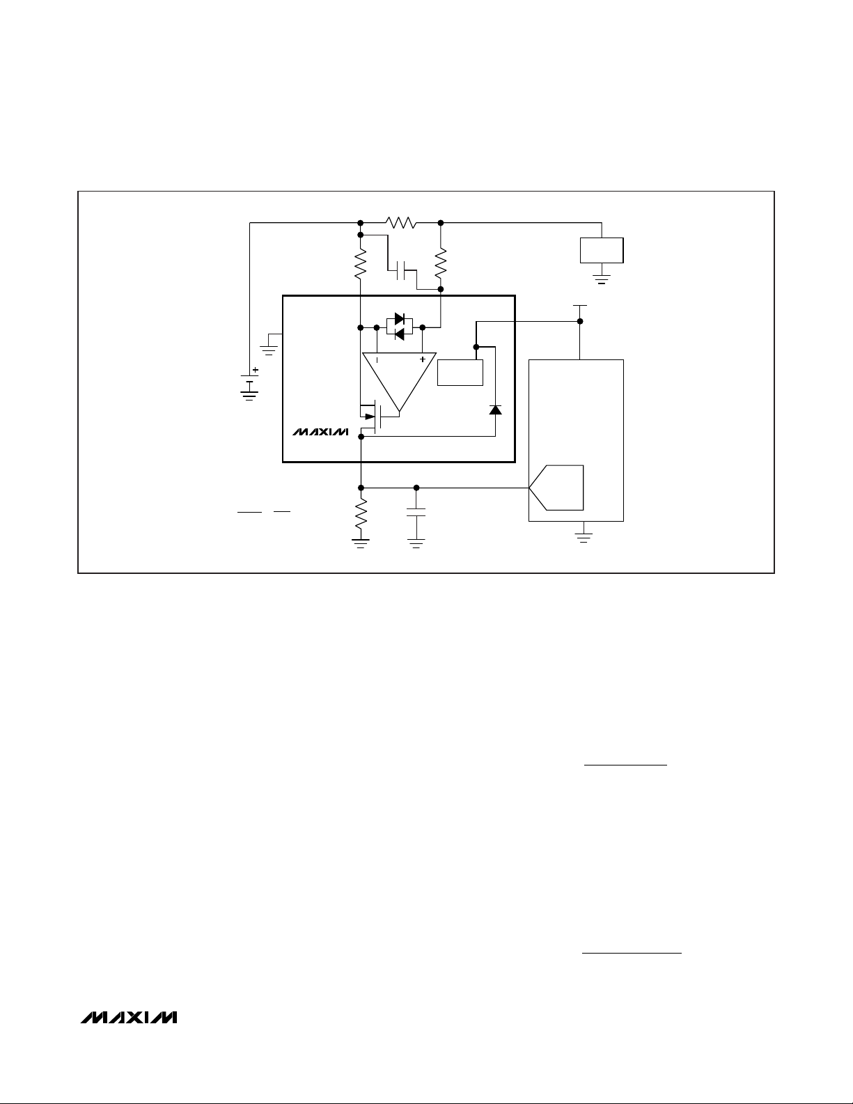
The MAX9937 allows two methods of filtering to help
improve performance in the presence of input commonmode voltage and input differential-voltage transients
(see Figure 1).
The capacitor CINbetween RS+ and RSN helps filter
against input differential voltages, and prevents them
from reaching the MAX9937. The corner frequency of
this filter is determined by the choice of R
RSN
and CIN.
Similarly, capacitor C
OUT
from OUT to ground helps filter the output voltage, thus providing not only differential filtering, but also filtering for input common-mode
transients that have made it past the MAX9937. The
corner frequency of this filter is similarly determined by
choice of R
OUT
and C
OUT
. Note: The MAX9937 is a
current-output device, and has the ability to drive an
infinite amount of load capacitance.
MAX9937
Automotive Current-Sense Amplifier
with Reverse-Battery Protection
_______________________________________________________________________________________ 9
Figure 1. Typical Application Circuit with Optional External Filtering
R
SENSE
RS+
CIN*
OUT
220nF
C
*
OUT
1nF
V
BAT
TO 28V
GAIN =
GND
= 4V
MAX9937
R
V
OUT
OUT
=
R
V
RSP
SENSE
*FILTER CAPACITORS ARE OPTIONAL.
R
RSP
499Ω
R
OUT
10kΩ
RSP
RS-
R
RSN
499Ω
RSN
BIAS
BLOCK
V
CC
MICROCONTROLLER
LOAD
5V
ADC
f
CIN
−
=
1
RC
2π
×
RSN IN
f
C OUT
−
=
2π
1
R COUT
×
OUT
Page 10

MAX9937
Automotive Current-Sense Amplifier
with Reverse-Battery Protection
10 ______________________________________________________________________________________
At frequencies below the output corner frequency, the
MAX9937 itself provides excellent 100dB (DC) common-mode rejection. At higher frequencies, as the
CMRR of the MAX9937 degrades, the output filter
formed by R
OUT
and C
OUT
helps boost the common-
mode rejection of the circuit.
Input Common-Mode Voltages
> 28V and < 0V
Short-duration overvoltages on the battery line are isolated from the RSP and RSN pins of the MAX9937 by
the use of input resistors R
RSP
and R
RSN
. The input
ESD clamp structure is designed so that the device can
withstand short-duration (< 1s) overvoltages up to 40V
when using resistors R
RSP
and R
RSN
of 500Ω or greater
as shown in the
Typical Application Circuit
.
Approximately 40mA flows out of each ESD diode during this condition (20V/500Ω). This current is less than
the 50mA absolute maximum specification for the RSN
and RSP pins.
Skewed Input Offset Voltage
for Production Calibration
Due to low temperature drift of input bias current and
input offset voltage in the MAX9937, the part can be
used to provide powerful application and system benefits not normally attainable from other current-sense
amplifiers on the market. For example, input resistors
R
RSP
and R
RSN
can be intentionally mismatched so as
to introduce an external, controlled input offset voltage
into the circuit. Doing so allows microcontroller firmware
to trim out input offset voltages completely by using
production-line calibration during the manufacturing
process or in system operation as long as a zero loadcurrent condition is forced. Only minimal temperaturedrift-based errors in the resistor and in the bias currents
then remain.
V
OS-FINAL
= VOS+ IB-x R
RSN
- IB+x R
RSP
while gain = R
OUT/RRSP
.
Since gain can be fixed by choosing R
OUT
and R
RSP
, a
positive offset voltage can be induced by varying the
value of R
RSN
compared to R
RSP
.
For example:
R
OUT
= 10kΩ, R
RSP
= 500Ω fixes gain = 20V/V. Now,
choosing R
RSN
= 2.5kΩ, and knowing ΔIB= ±12% of IB,
the additional VOSbecomes:
ΔVOS(max) = (5.6µA x 2500) ± (0.12 x 5.6µA x 2500) -
(5.6µA x 500) = 11.2mV ± 1.7mV
ΔVOS(min) = (0.8µA x 2500) ± (0.12 x 0.8µA x 2500) -
(0.8µA x 500) = 1.6mV ± 0.24mV
Since the minimum extra VOSintroduced into the part is
greater than the maximum V
OS
of the current-sense
amplifier (= 1mV), the output of the current-sense
amplifier is always greater than zero even at zero sense
voltage, thus allowing the current-sense amplifier to be
calibrated at zero input current.
Operation with VCC= 0V (Shutdown)
The input terminals go into a high-impedance mode
when VCC= 0, as shown by the input bias current in
shutdown 1µA specification. Due to the low 20µA supply current, this then becomes a convenient way to put
the amplifier in shutdown simply by using a digital I/O
port of a microcontroller to power up/down the currentsense amplifier. This can be especially useful in certain
battery-operated applications that need to implement
flexible power-management schemes.
GND
RSNOUT
1 5 RSPVCC
MAX9937
SC70
TOP VIEW
2
34
+
Pin Configuration
Chip Information
PROCESS: BiCMOS
Package Information
For the latest package outline information and land patterns, go
to www.maxim-ic.com/packages
.
PACKAGE TYPE PACKAGE CODE DOCUMENT NO.
5 SC70 X5+1
21-0076
Page 11

MAX9937
Automotive Current-Sense Amplifier
with Reverse-Battery Protection
Maxim cannot assume responsibility for use of any circuitry other than circuitry entirely embodied in a Maxim product. No circuit patent licenses are
implied. Maxim reserves the right to change the circuitry and specifications without notice at any time.
Maxim Integrated Products, 120 San Gabriel Drive, Sunnyvale, CA 94086 408-737-7600 ____________________
11
© 2008 Maxim Integrated Products is a registered trademark of Maxim Integrated Products, Inc.
Package Information (continued)
(The package drawing(s) in this data sheet may not reflect the most current specifications. For the latest package outline information
go to www.maxim-ic.com/packages
.)
SC70, 5L.EPS
PACKAGE OUTLINE, 5L SC70
21-0076
1
E
1
 Loading...