

Page 1
General Description
The MAX9918/MAX9919/MAX9920 are single-supply,
high-accuracy current-sense amplifiers with a high
input common-mode range that extends from -20V to
+75V. These amplifiers are well suited for current monitoring of inductive loads such as motors and solenoids,
where common-mode voltages can become negative
due to inductive kickback, reverse-battery conditions,
or transient events.
The MAX9918/MAX9920 feature adjustable gain set by
an external resistive-divider network. The MAX9919 features fixed gains of 45V/V (MAX9919F) and 90V/V
(MAX9919N). The MAX9918/MAX9919/MAX9920 operate as unidirectional amplifiers when V
REFIN
= GND
and as bidirectional amplifiers when V
REFIN
= VCC/2.
The MAX9920 attenuates the input signal by a factor of
4 at the input level-shifting stage allowing the device to
sense voltages up to 200mV (unidirectional operation)
or ±100mV (bidirectional operation).
The MAX9918/MAX9919/MAX9920 operate with a single 5V supply voltage, are fully specified over the -40°C
to +125°C automotive temperature range, and are
available in an 8-pin SOIC package.
Applications
H-Bridge Motor Current Sensing
Solenoid Current Sensing
Current Monitoring of Inductive Loads
High- and Low-Side Precision Current Sensing
4x4 Transmission Control
Electronic Throttle Control
Super-Capacitor Charge/Discharge Monitoring in
Hybrid Cars
Precision High-Voltage Current Monitoring
Features
♦ -20V to +75V Input Common-Mode Voltage Range
♦ 400µV (max) Input Offset Voltage
♦ 0.6% (max) Gain Accuracy Error
♦ Uni- or Bidirectional Current Sensing
♦ Reference Input for Bidirectional OUT
♦ 120kHz, -3dB Bandwidth (MAX9919N)
♦ Single-Supply Operation (4.5V to 5.5V)
♦ 1mA Supply Current
♦ 0.5µA (typ) Shutdown Current
♦ Rail-to-Rail Output
♦ -40°C to +125°C Automotive Temperature Range
MAX9918/MAX9919/MAX9920
-20V to +75V Input Range, Precision
Uni-/Bidirectional, Current-Sense Amplifiers
________________________________________________________________
Maxim Integrated Products
1
19-5015; Rev 1; 1/10
For pricing, delivery, and ordering information, please contact Maxim Direct at 1-888-629-4642,
or visit Maxim’s website at www.maxim-ic.com.
EVALUATION KIT
AVAILABLE
Typical Operating Circuit
Ordering Information/
Selector Guide
Note: All devices operate over the -40°C to +125°C temperature range.
+
Denotes a lead(Pb)-free/RoHS-compliant package.
*
EP = Exposed pad.
V
BATT
V
PART
MAX9918ASA+ ±50 Adjustable 8 SOIC-EP*
MAX9919FASA+ ±50 45 8 SOIC-EP*
MAX9919NASA+ ±50 90 8 SOIC-EP*
MAX9920ASA+ ±200 Adjustable 8 SOIC-EP*
SENSE
(mV)
GAIN
(V/V)
PIN-PACKAGE
V
V
CC
CC
φ1A
φ2B
R
SENSE
M
φ2B
RS+
RS-
φ1B
MAX9918
MAX9920
INPUT STAGE
LEVEL SHIFTER
SHDN
A
ADJUSTABLE GAIN
GND
OUT
R2
FB
R1
REFIN
REF
ADC
μC
GND
Page 2
MAX9918/MAX9919/MAX9920
-20V to +75V Input Range, Precision
Uni-/Bidirectional, Current-Sense Amplifiers
2 _______________________________________________________________________________________
ABSOLUTE MAXIMUM RATINGS
ELECTRICAL CHARACTERISTICS
(VCC= 5V, V
RS+
= V
RS-
= +14V, V
SENSE
= (V
RS+
- V
RS-
) = 0V, V
SHDN
= V
GND
= 0V, V
REFIN
= VCC/2, RL= 100kΩ; for MAX9918, AV=
90V/V, R2/R1 = 89kΩ/1kΩ; for MAX9920, A
V
= 20V/V, R2/R1 = 79kΩ/1kΩ; TA= -40°C to +125°C, unless otherwise noted. Typical val-
ues are at T
A
= +25°C.) (Note 1)
Stresses beyond those listed under “Absolute Maximum Ratings” may cause permanent damage to the device. These are stress ratings only, and functional
operation of the device at these or any other conditions beyond those indicated in the operational sections of the specifications is not implied. Exposure to
absolute maximum rating conditions for extended periods may affect device reliability.
VCCto GND..............................................................-0.3V to +6V
RS+, RS- to GND (V
CC
= 5V) ..................................-30V to +80V
RS+, RS- to GND (V
CC
= 0V) .............-15V to +80V (15 minutes)
Differential Input Voltage (V
RS+
- V
RS-
)
(MAX9918/MAX9919).................................±15V (Continuous)
Differential Input Voltage
(V
RS+
- V
RS-
) (MAX9920) .............................±5V (Continuous)
REFIN, FB, OUT to GND.............................-0.3V to (V
CC
+ 0.3V)
SHDN to GND.........................................................-0.3V to +20V
Output Short Circuit to V
CC
or GND...........................Continuous
Continuous Current into Any Pin
(Not to exceed package power dissipation) ................±20mA
Continuous Power Dissipation (T
A
= +70°C)
8-Pin SOIC-EP (derate 24.4mW/°C above +70°C) .1951.2mW**
SOIC Package Junction-to-Ambient
Thermal Resistance (θ
JA
) (Note 1)...............................41°C/W
Junction Temperature......................................................+150°C
Storage Temperature Range .............................-65°C to +150°C
Reflow Soldering Temperature ........................................+260°C
Lead Temperature (soldering, 10s) .................................+300°C
Note 1: Package thermal resistances were obtained using the method described in JEDEC specification JESD51-7, using a four-
layer board. For detailed information on package thermal considerations, refer to www.maxim-ic.com/thermal-tutorial
.
**
As per JEDEC51 Standard (multilayer board).
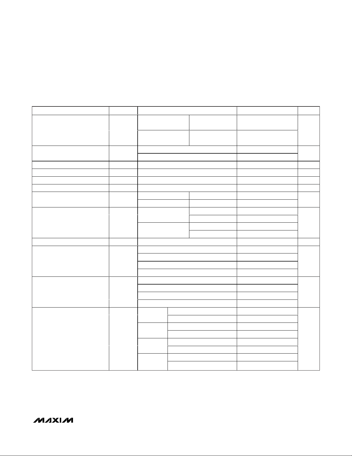
PARAMETER SYMBOL CONDITIONS MIN TYP MAX UNITS
MAX9918
Input Offset Voltage (Note 2) V
OS
MAX9919_
MAX9920
V
= V
RS+
+14V, V
= 0V
V
= V
RS+
-2V, V
0V
V
= V
RS+
+14V, V
= 0V
V
= V
RS+
-2V, V
0V
V
= V
RS+
+14V, V
= 0V
V
= V
RS+
-2V, V
0V
REFIN
REFIN
REFIN
RS-
REFIN
RS-
RS-
REFIN
RS-
RS-
REFIN
RS-
TA = +25°C ±0.14 ±0.4
=
T
A
= -40°C
to +125°C
TA = +25°C ±0.08 ±0.4
=
=
T
= -40°C
A
to +125°C
TA = +25°C ±0.18 ±0.4
=
= -40°C
T
A
to +125°C
TA = +25°C ±0.11 ±0.4
=
=
T
= -40°C
A
to +125°C
TA = +25°C ±0.48 ±1.2
=
= -40°C
T
A
to +125°C
TA = +25°C ±0.10 ±0.9
=
=
= -40°C
T
A
to +125°C
±0.7
±1.3
±0.9
±1.0
±3.0
±3.5
mV
Page 3
MAX9918/MAX9919/MAX9920
-20V to +75V Input Range, Precision
Uni-/Bidirectional, Current-Sense Amplifiers
_______________________________________________________________________________________ 3
ELECTRICAL CHARACTERISTICS (continued)
(VCC= 5V, V
RS+
= V
RS-
= +14V, V
SENSE
= (V
RS+
- V
RS-
) = 0V, V
SHDN
= V
GND
= 0V, V
REFIN
= VCC/2, RL= 100kΩ; for MAX9918, AV=
90V/V, R2/R1 = 89kΩ/1kΩ; for MAX9920, A
V
= 20V/V, R2/R1 = 79kΩ/1kΩ; TA= -40°C to +125°C, unless otherwise noted. Typical val-
ues are at T
A
= +25°C.) (Note 1)
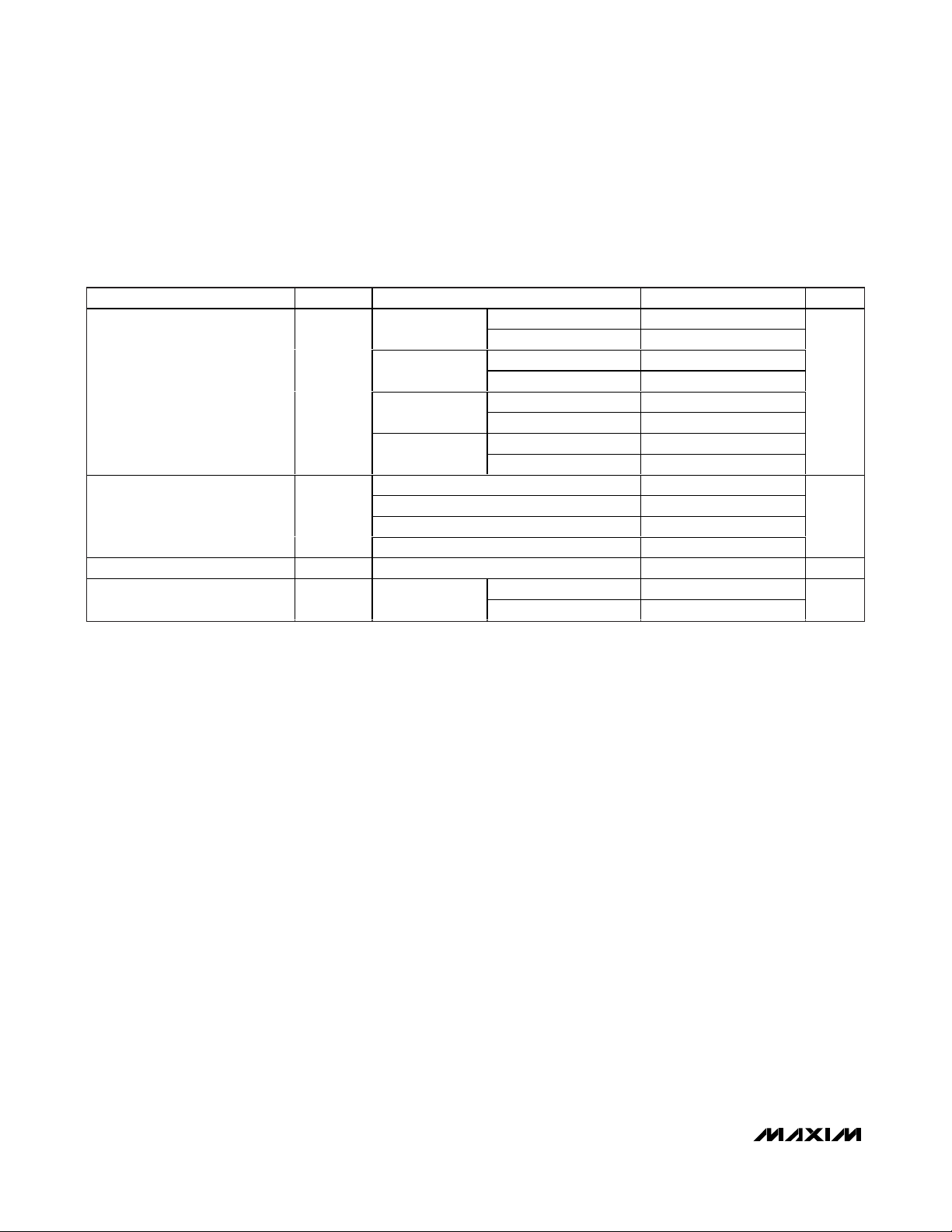
Input Offset Voltage Drift
(Note 3)
Common-Mode Range V
Common-Mode Rejection Ratio
(Note 3)
Input Bias Current I
Input Offset Current ( I
Input Leakage Current in
Shutdown
Input Leakage Current V
Input Resistance
Full-Scale Sense Voltage (Note 4) V
Minimum Adjustable Gain G
PARAMETERS SYMBOL CONDITIONS MIN TYP MAX UNITS
MAX9918
V
OSD
MAX9919_
MAX9920
CM
Inferred from CMRR tests -20 +75 V
M AX 9918, M AX 9919
CMRR
MAX9920
, I
RS+
RS +
-20V ≤ VCM ≤ +75V
RS-
- I
) 0 ±8 μA
RS -
-20V ≤ V
RS+
≤ +75V, V
CM
= V
= +14V, +75V, V
RS-
MAX9918,
MAX9919_
MAX9920
SENSE
Inferred from gain
error test
MAX9918, MAX9920 Adj
MAX9919F 45Gain (Notes 2, 4) G
MAX9919N 90
ADJ
MAX9918 30
MAX9920 7.5
V
V
V
V
V
V
RS+
RS+
RS+
RS+
RS+
RS+
= V
RS-
= V
RS-
= V
RS-
= V
RS-
= V
RS-
= V
RS-
= +14V ±1.2
= -2V ±3.3
= +14V ±1.8
= -2V ±1.8
= +14V ±2.4
= -2V ±8.8
-2V ≤ VCM ≤ +14V 80
-20V ≤ V
≤ +75V 96
CM
-2V ≤ VCM ≤ +14V 72
-20V ≤ V
≤ +75V 86
CM
TA = +25°C ±175
= -40°C to +125°C ±250
T
A
= V
SHDN
= 5V ±30 μA
CC
= 0V ±30 μA
CC
Common mode 300 kΩ
Differential 715 Ω
Common mode 330 kΩ
Differential 224 Ω
MAX9918, MAX9919_ 50
MAX9920 200
μV/°C
dB
μA
mV
V/V
V/V
Page 4
MAX9918/MAX9919/MAX9920
-20V to +75V Input Range, Precision
Uni-/Bidirectional, Current-Sense Amplifiers
4 _______________________________________________________________________________________
ELECTRICAL CHARACTERISTICS (continued)
(VCC= 5V, V
RS+
= V
RS-
= +14V, V
SENSE
= (V
RS+
- V
RS-
) = 0V, V
SHDN
= V
GND
= 0V, V
REFIN
= VCC/2, RL= 100kΩ; for MAX9918, AV=
90V/V, R2/R1 = 89kΩ/1kΩ; for MAX9920, A
V
= 20V/V, R2/R1 = 79kΩ/1kΩ; TA= -40°C to +125°C, unless otherwise noted. Typical val-
ues are at T
A
= +25°C.) (Note 1)
Gain Error
(Note 2)
FB Input Bias Current I
Output-Voltage High (Note 4) VCC - V
Output-Voltage Low (Note 4) V
Short-Circuit Current I
Output Resistance R
REFIN Voltage Range
PARAMETER SYMBOL CONDITIONS MIN TYP MAX UNITS
GE
FB
OL
SC
OUT
TA = +25°C,
V
= 0V
REFIN
=
= -40°C to
T
A
+125°C,
= 0V
V
REFIN
TA = +25°C ±0.02 ±0.6
=
=
T
= -40°C to
A
+125°C
TA = +25°C ±0.13 ±0.45
=
=
T
= -40°C to
A
+125°C
TA = +25°C ±0.10 ±0.45
=
=
= -40°C to
T
A
+125°C
TA = +25°C ±0.16 ±0.6
=
=
= -40°C to
T
A
+125°C
TA = +25°C ±0.11 ±0.6
=
=
T
= -40°C to
A
+125°C
TA = +25°C ±0.29 ±1.0
=
=
T
= -40°C to
A
+125°C
TA = +25°C ±0.24 ±1.0
=
=
= -40°C to
T
A
+125°C
MAX9918
MAX9919F
MAX9919N
MAX9920
V
= V
RS+
+14V
V
= V
RS+
-2V, V
0V
V
= V
RS+
+14V, V
0V
= V
V
RS+
-2V, V
0V
V
= V
RS+
+14V, V
0V
V
= V
RS+
-2V, V
0V
V
= V
RS+
+14V, V
0V
V
= V
RS+
-2V, V
0V
RS-
RS-
REFIN
RS-
REFIN
RS-
REFIN
RS-
REFIN
RS-
REFIN
RS-
REFIN
RS-
REFIN
MAX9918, MAX9920 5 15 nA
V
= 200mV for
SENSE
MAX9918, MAX9919_,
OH
V
= 400mV for
SENSE
MAX9920
V
= -200mV for
SENSE
MAX9918, MAX9919_,
V
= -400mV for
SENSE
MAX9920
OUT shorted to V
RL = 100kΩ to GND 3 10
R
= 10kΩ to GND 12 40
L
CC
RL = 100kΩ to V
R
= 10kΩ to V
L
CC
CC
OUT shorted to GND 41
M AX 9918, M AX9919_ 0
Inferred from REFIN
CMRR test
MAX9920 0
±0.08 ±0.6
310
10 40
44
0.1 Ω
V
CC
/2
V
CC
/2
±1.2
±1.0
±1.2
±0.9
±1.2
±1.0
±1.7
±1.7
V
CC
1.9
V
CC
2.4
%
mV
mV
mA
-
V
-
Page 5
MAX9918/MAX9919/MAX9920
-20V to +75V Input Range, Precision
Uni-/Bidirectional, Current-Sense Amplifiers
_______________________________________________________________________________________ 5
ELECTRICAL CHARACTERISTICS (continued)
(VCC= 5V, V
RS+
= V
RS-
= +14V, V
SENSE
= (V
RS+
- V
RS-
) = 0V, V
SHDN
= V
GND
= 0V, V
REFIN
= VCC/2, RL= 100kΩ; for MAX9918, AV=
90V/V, R2/R1 = 89kΩ/1kΩ; for MAX9920, A
V
= 20V/V, R2/R1 = 79kΩ/1kΩ; TA= -40°C to +125°C, unless otherwise noted. Typical val-
ues are at T
A
= +25°C.) (Note 1)
REFIN Common-Mode Rejection
Ratio
REFIN Current I
SHDN Logic-High V
SHDN Logic-Low V
SHDN Logic Input Current 0 ≤ V
Supply Voltage Range V
Power-Supply Rejection Ratio
(Note 3)
Supply Current I
Shutdown Supply Current I
Small Signal -3dB Bandwidth BW
Slew Rate SR
1% Settling Time from V
Step
PARAMETERS SYMBOL CONDITIONS MIN TYP MAX UNITS
MAX9918, MAX9919_
RE FIN
C M R R
MAX9920
REFIN
CC
PSRR
CC
CC_SHDNVSHDN
M AX 9918, M AX 9919_, V
MAX9920, V
IH
IL
SHDN
≤ V
RS+
= V
CC
Inferred from PSRR test 4.5 5.5 V
MAX9918, MAX9919_ 4.5V ≤ V
MAX9920 4.5V ≤ V
V
= V
= V
RS-
RS-
= +14V
= -2V
V
RS+
RS+
= VCC = 5V 0.5 10 μA
MAX9918, V
MAX9919F, V
MAX9919N, V
MAX9920, V
SENSE
SENSE
SENSE
SENSE
MAX9918 0.6
MAX9919F 0.9
MAX9919N 3.0
MAX9920 1.5
V
MAX9918
MAX9919F
SENSE
MAX9919N
MAX9920
SENSE
V
SENSE
V
SENSE
V
SENSE
V
SENSE
V
SENSE
V
S E N S E
V
S E N S E
0V ≤ V
REFIN
- 1.9V)
0V ≤ V
REFIN
- 2.4V)
= V
RS +
RS -
= ±200mV ±100
RS-
≤ (V
≤ (V
CC
CC
82 103
75 90
= ± 50m V ±100
2.0 V
≤ 5.5V 74 103
CC
≤ 5.5V 68 100
CC
TA = +25°C 0.7 1.2
T
= - 40°C to + 125°C 1.5
A
TA = +25°C 1.0 1.6
T
= - 40°C to + 125°C 2.2
A
= 50mV 75
= 50mV 250
= 50mV 120
= 200mV 230
= 5mV to 50mV step 12
= 50mV to 5mV step 7
= 5mV to 50mV step 3.5
= 50mV to 5mV step 2.5
= 5mV to 50mV step 3.5
= 50mV to 5mV step 3
= 20m V to 200m V step 5
= 200m V to 20m V ste p 3
dB
μA
0.8 V
5μA
dB
mA
kHz
V/μs
μs
Page 6
MAX9918/MAX9919/MAX9920
-20V to +75V Input Range, Precision
Uni-/Bidirectional, Current-Sense Amplifiers
6 _______________________________________________________________________________________
ELECTRICAL CHARACTERISTICS (continued)
(VCC= 5V, V
RS+
= V
RS-
= +14V, V
SENSE
= (V
RS+
- V
RS-
) = 0V, V
SHDN
= V
GND
= 0V, V
REFIN
= VCC/2, RL= 100kΩ; for MAX9918, AV=
90V/V, R2/R1 = 89kΩ/1kΩ; for MAX9920, A
V
= 20V/V, R2/R1 = 79kΩ/1kΩ; TA= -40°C to +125°C, unless otherwise noted. Typical val-
ues are at T
A
= +25°C.) (Note 1)
Note 1: All devices are 100% production tested at TA= +25°C. All temperature limits are guaranteed by design.
Note 2: V
OS
is extrapolated from two point gain error tests. Measurements are made at V
SENSE
= 5mV and 50mV for
MAX9918/MAX9919N/MAX9919F, and V
SENSE
= 20mV and 200mV for MAX9920.
Note 3: Extrapolated V
OS
as described above in Note 2 is used to calculate VOSdrift, CMRR, and PSRR.
Note 4: OUT should be 100mV away from either rail to achieve rated accuracy, or limited by a V
SENSE
of 50mV for the
MAX9918/MAX9919N/MAX9919F and 200mV for the MAX9920.
Note 5: Not production tested. Guaranteed by design.
1% Settling Time from VCM Step
Power-Up Time
Max Capacitive Load Stability No sustained oscillations (Note 5) 50 pF
Input Referred Noise Voltage
Density
PARAMETERS SYMBOL CONDITIONS MIN TYP MAX UNITS
e
n
MAX9918,
V
= 50mV
SENSE
MAX9919F,
V
= 50mV
SENSE
MAX9919N,
V
= 50mV
SENSE
MAX9920,
V
= 200mV
SENSE
MAX9918, V
MAX9919F, V
MAX9919N, V
MAX9920, V
10kHz
VCM = -2V to +14V step 2.5
V
VCM = -2V to +14V step 2.5
V
VCM = -2V to +14V step 3.5
V
VCM = -2V to +14V step 0.25
V
= 50mV, 1% settling 4.5
SENSE
= 50mV, 1% settling 5
SENSE
= 50mV, 1% settling 6
SENSE
= 200mV, 1% settling 5
SENSE
MAX9918, MAX9919_ 60
MAX9920 174
= +14V to -2V step 0.5
CM
= +14V to -2V step 0.5
CM
= +14V to -2V step 3.5
CM
= +14V to -2V step 2.5
CM
μs
μs
nV/√Hz
Page 7

MAX9918/MAX9919/MAX9920
-20V to +75V Input Range, Precision
Uni-/Bidirectional, Current-Sense Amplifiers
_______________________________________________________________________________________ 7
Typical Operating Characteristics
(VCC= 5V, TA= +25°C, unless otherwise noted.)
0 0.1 0.2 0.3-0.4 -0.3 -0.2 -0.1 0.4
GAIN ERROR (%)
MAX9918 toc08
N (%)
0.1
0.2
0.3
0.4
0.5
0.6
0.7
0.8
0
GAIN ERROR
(V
RS+
= +14V, MAX9919N, AV = +90V/V)
V
OS
(V
= +14V)
0.50
0.45
0.40
0.35
0.30
0.25
N (%)
0.20
0.15
0.10
0.05
0
-400 400
RS+
MAX9918 toc01
240 320-240-160 -80 0 80 160-320
OFFSET VOLTAGE (FV)
VOS DRIFT
(V
= -2V)
0.45
0.40
0.35
0.30
0.25
N (%)
0.20
0.15
0.10
0.05
0
-10 10
RS+
MAX9918 toc04
846-6 -4 -2 0 2-8
OFFSET VOLTAGE (FV/°C)
VOS DRIFT
(V
= +14V)
0.30
0.25
0.20
0.15
N (%)
0.10
0.05
0
-4 4
500
400
300
200
100
(uV)
0
OS
V
-100
-200
MAX9918ASA
-300
V
CC
-400
V
REF
-500
-20 80
RS+
OFFSET VOLTAGE (FV/°C)
VOS vs. V
TA = -40°C
TA = +25°C
TA = +125°C
= 5V
= GND
VCM (V)
CM
V
OS
(V
= -2V)
0.35
0.30
MAX9918 toc02
0.25
0.20
N (%)
0.15
0.10
0.05
3210-1-2-3
MAX9918 toc05
706040 500 10 20 30-10
0
-400 400
125
100
75
50
25
0
VOS (FV)
-25
-50
MAX9918ASA
VCC = 5V
-75
V
= GND
REF
-100
4.5 5.5
RS+
OFFSET VOLTAGE (FV)
VOS vs. V
CC
VCC (V)
MAX9918 toc03
320240160800-80-160-240-320
MAX9918 toc06
VCM = 14V
VCM = -2V
5.45.35.1 5.24.7 4.8 4.9 5.04.6
GAIN ERROR
N (%)
(V
RS+
0.6
0.5
0.4
0.3
0.2
0.1
0
(V
= +14V, MAX9919F, AV = +45V/V)
RS+
0.6
0.5
0.4
0.3
N (%)
0.2
0.1
0
GAIN ERROR (%)
0 0.1 0.2 0.3-0.4 -0.3 -0.2 -0.1
MAX9918 toc07
0.4
GAIN ERROR
= -2V, MAX9919F, AV = +45V/V)
MAX9918 toc09
0 0.1 0.2 0.3-0.4 -0.3 -0.2 -0.1 0.4
GAIN ERROR (%)
Page 8

MAX9918/MAX9919/MAX9920
-20V to +75V Input Range, Precision
Uni-/Bidirectional, Current-Sense Amplifiers
8 _______________________________________________________________________________________
Typical Operating Characteristics (continued)
(VCC= 5V, TA= +25°C, unless otherwise noted.)
0.6
0.5
0.4
0.3
N (%)
0.2
0.1
(V
GAIN ERROR
= -2V, MAX9919N, AV = +90V/V)
RS+
MAX9918 toc10
0
0 0.1 0.2 0.3-0.4 -0.3 -0.2 -0.1 0.4
GAIN ERROR (%)
2.0
1.6
1.2
0.8
0.4
0
GE (%)
-0.4
-0.8
-1.2
-1.6
-2.0
-20 80
GAIN ERROR vs. V
TA = +125NC
TA = +25NC
MAX9918ASA
VCC = 5V
V
= GND
REF
CM
MAX9918 toc11
TA = -40NC
706040 500 10 20 30-10
VCM (V)
0.5
GAIN ERROR vs. V
0.4
0.3
0.2
0.1
VCM = -2V
CC
0.25
0.20
MAX9918 toc12
0.15
0.10
0.05
0
-0.1
GAIN ERROR (%)
-0.2
-0.3
VCM = 14V
-0.4
-0.5
4.5 5.5
5.35.14.94.7
-0.05
LINEARITY (%)
-0.10
-0.15
-0.20
-0.25
VCC (V)
0.10
LINEARITY vs. V
0.08
0.06
0.04
0.02
0
-0.02
LINEARITY (%)
-0.04
-0.06
-0.08
-0.10
-30 30
T
A
TA = +125°C
V
= -40°CTA = +25°C
SENSE
(mV)
SENSE
VCM = +14V
VCC = 5V
V
= VCC/2
REFIN
AV = 90V/V
BIDIRECTIONAL
20100-10-20
MAX9918 toc14
0.10
0.08
0.06
0.04
0.02
-0.02
LINEARITY (%)
-0.04
-0.06
-0.08
-0.10
LINEARITY vs. V
= -40°C
T
A
0
TA = +125°C
-30 30
TA = +25°C
V
LINEARITY vs. V
T
TA = +25°C
0
A
TA = +125°C
V
SENSE
= -40°C
SENSE
SENSE
VCM = -2V
VCC = 5V
V
REFIN
AV = 90V/V
BIDIRECTIONAL
(mV)
SENSE
VCM = -2V
VCC = 5V
V
REFIN
AV = 90V/V
UNIDIRECTIONAL
(mV)
= VCC/2
20100-10-20
= GND
706040 5020 3010080
MAX9918 toc13
MAX9918 toc15
Page 9

MAX9918/MAX9919/MAX9920
-20V to +75V Input Range, Precision
Uni-/Bidirectional, Current-Sense Amplifiers
_______________________________________________________________________________________ 9
Typical Operating Characteristics (continued)
(VCC= 5V, TA= +25°C, unless otherwise noted.)
LINEARITY vs. V
0.20
0.18
0.16
0.14
0.12
0.10
0.08
0.06
0.04
0.02
LINEARITY (%)
-0.02
-0.04
-0.06
-0.08
-0.10
VCM = +14V
= 5V
V
CC
= GND
V
REFIN
= 90V/V
A
V
UNIDIRECTIONAL
TA = +25°C
0
TA = +125°C
5
070
V
SENSE
LINEARITY vs. V
0.10
0.08
0.06
0.04
0.02
-0.02
LINEARITY (%)
-0.04
-0.06
-0.08
-0.10
TA = -40°C
TA = +125°C
0
TA = +25°C
-20-80-100 100
-60
-40
V
30 35
SENSE
SENSE
TA = -40°C
40 45
(mV)
SENSE
(mV)
65
6055
5010 15 20 25
VCM = +14V
= 5V
V
CC
= VCC/2
V
REFIN
= 30V/V
A
V
BIDIRECTIONAL
806002040
MAX9918 toc16
MAX9918 toc18
LINEARITY vs. V
0.25
0.20
0.15
0.10
0.05
0
-0.05
LINEARITY (%)
-0.10
-0.15
-0.20
-0.25
6.0
5.5
5.0
4.5
4.0
3.5
(V)
3.0
REFIN
2.5
- V
2.0
OUT
V
1.5
1.0
0.5
0
-0.5
-1.0
TA = +25°C
TA = +125°C
-60
-40
V
OUT - VREFIN
-20-80
V
SENSE
-100 100
-2V VCM: SOLID LINE
: DASHED LINE
14V V
CM
-20 80
V
SENSE
SENSE
VCM = -2V
VCC = 5V
V
REFIN
= 30V/V
A
V
BIDIRECTIONAL
TA = -40°C
(mV)
vs. V
SENSE
MAX9918, V
UNIDIRECTIONAL,
REFIN
GAIN = 90V/V
(mV)
= VCC/2
= 0V
MAX9918 toc17
806002040
MAX9918 toc19
706040 500 10 20 30-10
V
- V
3.0
-2V VCM: SOLID LINE
2.5
14V V
2.0
OUT
: DASHED LINE
CM
REFIN
vs. V
SENSE
1.5
1.0
(V)
0.5
REFIN
0
- V
-0.5
OUT
V
-1.0
-1.5
-2.0
-2.5
MAX9918, V
BIDIRECTIONAL,
REFIN
GAIN = 90V/V
-3.0
-40 40
V
(mV)
SENSE
= VCC/2
30200 10-20 -10-30
MAX9918 toc20
350
VCM = +14V
300
250
(mV)
200
OL
150
AND V
OH
V
100
50
0
010
VOH/VOL vs. I
VCC - V
IOH (mA)
OH
MAX9918 toc21
OH
V
OL
987654321
Page 10

MAX9918/MAX9919/MAX9920
-20V to +75V Input Range, Precision
Uni-/Bidirectional, Current-Sense Amplifiers
10 ______________________________________________________________________________________
Typical Operating Characteristics (continued)
(VCC= 5V, TA= +25°C, unless otherwise noted.)
I
CC
vs.V
CM
MAX9918 toc23
VCM (V)
I
CC
(mA)
706040 500 10 20 30-10
0.5
0.6
0.7
0.8
0.9
1.0
1.1
1.2
1.3
1.4
1.5
1.6
0.4
-20 80
TA = +125NC
TA = +25NC
TA = -40NC
V
SENSE
= 0V (DASH)
V
SENSE
+ 50mV (SOLID)
PSRR vs. FREQUENCY
MAX9918 toc30
FREQUENCY (kHz)
PSRR (dB)
1k1001010.10.010.001
-120
-100
-80
-60
-40
-20
0
-140
0.0001 10k
MAX9918
V
CM
= 14V
V
SENSE
= 50mV
I
ICC vs. V
1.0
0.9
0.8
0.7
0.6
(mA)
0.5
CC
I
0.4
0.3
0.2
0.1
V
= 0V
SENSE
0
4.5 5.5
CC
VCM = -2V
VCM = 14V
VCC (V)
100
80
MAX9918 toc22
5.45.35.1 5.24.7 4.8 4.9 5.04.6
60
40
20
(FA)
0
BAIS
I
-20
-40
-60
-80
-100
-20 80
BIAS
MAX9918
VCC = 5V
vs. V
VCM (V)
CM
MAX9918 toc24
706040 500 10 20 30-10
INPUT LEAKAGE CURRENT vs. V
20
15
TA = +25NC
10
5
0
-5
-10
-15
-20
-25
-30
-35
INPUT LEAKAGE CURRENT (FA)
-40
-45
-50
-20 80
TA = +125NC
IN+ - IN- = 50mV
VCC = V
SHDN
V
= 0V
REFIN
GAIN vs. FREQUENCY
40
30
20
10
0
-10
GAIN (dB)
-20
-30
-40
-50
-60
MAX9920
= 14V
V
CM
GAIN = 20V/V
0.001 10
FREQUENCY (MHz)
= 0V
VCM (V)
TA = -40NC
10.10.01
CM
6040200
1000
MAX9918 toc25
(I)
IN
DIFFERENTIAL R
900
800
700
600
500
400
300
200
100
0
DIFFERENTIAL RIN vs. V
-20 70
VCM (V)
CM
55402510-5
GAIN vs. FREQUENCY
50
40
MAX9918 toc26
30
20
10
0
GAIN (dB)
-10
-20
MAX9918
VCM = 14V
-30
GAIN = 90V/V
-40
0.001 10
FREQUENCY (MHz)
MAX9918 toc27
10.10.01
GAIN vs. FREQUENCY
10
MAX9918
0
= 14V
V
CM
MAX9918 toc28
-10
GAIN = 90V/V
-20
-30
-40
-50
GAIN (dB)
-60
-70
-80
-90
-100
VCM = -2V
VCM = 14V
0.001 100
FREQUENCY (MHz)
1010.10.01
MAX9918 toc29
Page 11

MAX9918/MAX9919/MAX9920
-20V to +75V Input Range, Precision
Uni-/Bidirectional, Current-Sense Amplifiers
______________________________________________________________________________________ 11
Typical Operating Characteristics (continued)
(VCC= 5V, TA= +25°C, unless otherwise noted.)
SMALL-SIGNAL TRANSIENT
(GAIN = 45V/V)
5mV/div
50mV/div
MAX9918, VCM = 14V
V
= 10mV TO 15mV
SENSE
10Fs/div
LARGE-SIGNAL TRANSIENT
(GAIN = 45V/V)
50mV/div
SMALL-SIGNAL TRANSIENT
MAX9918 toc31
MAX9918 toc33
5mV/div
100mV/div
50mV/div
(GAIN = 90V/V)
MAX9918, VCM = 14V
V
= 10mV TO 15mV
SENSE
10Fs/div
LARGE-SIGNAL TRANSIENT
(GAIN = 90V/V)
MAX9918 toc32
MAX9918 toc34
500mV/div
MAX9918, VCM = 14V
V
= 0V TO 50mV
SENSE
10Fs/div
1V/div
MAX9918, VCM = 14V
V
= 0 TO 50mV
SENSE
10Fs/div
OUTPUT RESPONSE TO
10V/div
1V/div
COMMON-MODE STEP RESPONSE
MAX9918, VCM = 14V
S
10Fs/div
SENSE
MAX9918 toc35
= PS (50mV)
COMMON-MODE TRANSIENT
0
OUTPUT AC-COUPLED
FULL SCALE
AT THE INPUT
4µs/div
MAX9918 toc36
V
CM
50V/div
V
OUT
100mV/div
Page 12

MAX9918/MAX9919/MAX9920
-20V to +75V Input Range, Precision
Uni-/Bidirectional, Current-Sense Amplifiers
12 ______________________________________________________________________________________
Typical Operating Characteristics (continued)
(VCC= 5V, TA= +25°C, unless otherwise noted.)
5V/div
1V/div
SHUTDOWN ON/OFF DELAY
MAX9918, VCM = 14V
V
SENSE
4Fs/div
MAX9918 toc37
5V/div
2V/div
= PS (50mV)
OUTPUT OVERDRIVE
RECOVERY (30V/V)
MAX9918, VCM = 14V
V
200mV/div
SENSE
MAX9918 toc39
= 2 x PS
50mV/div
POWER-UP TIME
MAX9918, VCM = 14V
= PS (50mV)
V
SENSE
4Fs/div
OUTPUT OVERDRIVE
RECOVERY (90V/V)
MAX9918 toc38
MAX9918 toc40
2V/div
4Fs/div
2V/div
MAX9918, VCM = 14V
V
= 2 x PS
SENSE
4Fs/div
Page 13

Detailed Description
The MAX9918/MAX9919/MAX9920 are single-supply,
high-accuracy uni-/bidirectional current-sense amplifiers
with a high common-mode input range that extends from
-20V to +75V. The MAX9918/MAX9919/MAX9920’s input
stage utilizes a pair of level shifters allowing a wide
common-mode operating range when measuring the
voltage drop (V
SENSE
) across the current-sense resistor.
The first level shifter accommodates the upper commonmode operating range from +2V to +75V. When the
common-mode voltage falls below +2V, the second level
shifter is used to accommodate negative voltages down
to -20V.
The level shifters translate V
SENSE
to an internal reference voltage where it is then amplified with an instrumentation amplifier. The instrumentation amplifier
configuration provides high precision with input offset
voltages of 400μV (max). Indirect feedback of the
instrumentation amplifier allows the gain to be adjusted
with an external resistive-divider network on the
MAX9918/MAX9920. The MAX9919 is a fixed gain
device available with laser-trimmed resistors for gains
of 45V/V (MAX9919F) and 90V/V (MAX9919N).
The MAX9918/MAX9919 operate with a full-scale sense
voltage of 50mV. The input stage of the MAX9920 provides an attenuation factor of 4, enabling a full-scale
sense voltage of 200mV.
MAX9918/MAX9919/MAX9920
-20V to +75V Input Range, Precision
Uni-/Bidirectional, Current-Sense Amplifiers
______________________________________________________________________________________ 13
Pin Description
Pin Configuration
TOP VIEW
+
1
RS+
MAX9918
2RS-
MAX9919
3
4
MAX9920
8 SOIC-EP
SHDN
GND
*EXPOSED PAD. CONNECT EP TO SOLID GROUND FOR
PROPER THERMAL AND ELECTRICAL PERFORMANCE.
EP*
87V
6
5
CC
REFIN
FB
OUT
PIN NAME FUNCTION
1 RS+ Positive Current-Sensing Input. Power side connects to external sense resistor.
2 RS- Negative Current-Sensing Input. Load side connects to external sense resistor.
3 SHDN Active-High Shutdown Input. Connect to GND for normal operation.
4 GND Ground
5 OUT Current-Sense Output. V
Feedback Input. Connect FB to a resistive-divider network to set the gain for the MAX9918 and
6FB
MAX9920. See the Adjustable Gain (MAX9918/MAX9920) section for more information. Leave FB
unconnected for the MAX9919 for proper operation.
is proportional to V
OUT
SENSE
.
7 REFIN
8VCC5V Supply Voltage Input. Bypass VCC to GND with 0.1μF capacitor.
—EP
Reference Input. Set REFIN to V
operation.
Exposed Pad. Connect to a large-area contiguous ground plane for improved power dissipation. Do
not use as the only ground connection for the part.
/2 for bidirectional operation. Set REFIN to GND for unidirectional
CC
Page 14

Uni-/Bidirectional Operation
The MAX9918/MAX9919/MAX9920 support both unidirectional and bidirectional operation. The devices operate in unidirectional mode with V
REFIN
= GND. The
output is then referenced to ground and the output voltage V
OUT
is proportional to the positive voltage drop
(V
SENSE
) from RS+ to RS- (Figure 1).
The MAX9918/MAX9919 operate in bidirectional mode
by application of a low-source impedance reference
voltage in the 0V to V
CC
- 1.9V range, (typically VCC/2),
to REFIN. For the MAX9920, the reference voltage range
is 0V to V
CC
- 2.4V (typically VCC/2). The output voltage
V
OUT
relative to V
REFIN
is then proportional to the
±V
SENSE
voltage drop from RS+ to RS- (Figure 2).
MAX9918/MAX9919/MAX9920
-20V to +75V Input Range, Precision
Uni-/Bidirectional, Current-Sense Amplifiers
14 ______________________________________________________________________________________
Figure 1. Unidirectional Operation
Figure 2. Bidirectional Operation
I
DISCHARGE
5V
V
SHDN
RS+ RS-
MAX9919N
CC
R
SENSE
GND
OUT
REFIN
LOAD
TO ADC
V
OUT
3.6V
2.7V
1.8V
0.9V
0
G = 90V/V
DISCHARGE
CURRENT
20mV20mV
30mV10mV
V
SENSE
V
- V
OUT
REFIN
0
-0.9V
-1.8V
1.8V
0.9V
10mV
I
DISCHARGE
R
SENSE
RS+ RS-
MAX9919N
V
5V
CC
SHDN
GND
I
CHARGE
OUT
REFIN
TO ADC
2.5V
LOAD
-20mV
CHARGE
CURRENT
-10mV
G = 90V/V
DISCHARGE
CURRENT
20mV
V
SENSE
Page 15

Shutdown Mode
Drive SHDN high to enter low-power shutdown mode.
In shutdown mode, the MAX9918/MAX9919/MAX9920
draw 0.5μA (typ) of quiescent current.
Adjustable Gain (MAX9918/MAX9920)
The MAX9918/MAX9920 feature externally adjustable
gain set by a resistive-divider network circuit using
resistors R1 and R2 (see the
Functional Diagram
). The
gain frequency compensation is set for a minimum gain
of 30V/V for the MAX9918 and 7.5V/V for the MAX9920.
The gain G for the MAX9918/MAX9920 is given by the
following equation:
Applications Information
Component Selection
Ideally, the maximum load current develops the fullscale sense voltage across the current-sense resistor.
Choose the gain needed to yield the maximum output
voltage required for the application:
V
OUT
= V
SENSE
x G
where V
SENSE
is the full-scale sense voltage, 50mV for
the MAX9918/MAX9919, or 200mV for the MAX9920
and G is the gain of the device. G is externally
adjustable for the MAX9918/MAX9920. The MAX9919
has a fixed gain version of 45V/V (MAX9919F) or 90V/V
(MAX9919N).
In unidirectional applications (V
REFIN
= 0V), select the
gain of the MAX9918/MAX9920 to utilize the full output
range between GND and VCC. In bidirectional applications (V
REFIN
= VCC/2), select the gain to allow an output
voltage range of ±VCC/2. V
OUT
must be at least 100mV
from either rail to achieve the rated gain accuracy.
Sense Resistor, R
SENSE
Choose R
SENSE
based on the following criteria:
Accuracy: A high R
SENSE
value allows lower currents
to be measured more accurately. This is because offsets become less significant when the sense voltage is
larger. In the linear region (100mV < V
OUT
< V
CC
- 100mV), there are two components to accuracy: input
offset voltage (V
OS
) and gain error (GE). Use the linear
equation to calculate total error:
V
OUT
= (G ± GE) x (V
SENSE ±VOS
)
For best performance, select R
SENSE
to provide
approximately 50mV (MAX9918/MAX9919) or 200mV
(MAX9920) of sense voltage for the full-scale current in
each application. Sense resistors of 5mΩ to 100mΩ are
available with 1% accuracy or better.
Efficiency and Power Dissipation
At high current levels, the I2R losses in R
SENSE
can be
significant. Take this into consideration when choosing
the resistor value and its power dissipation (wattage)
rating. Also, the sense resistor’s value might drift if it is
allowed to heat up excessively. The precision V
OS
of
the MAX9918/MAX9919/MAX9920 allows the use of
small sense resistors to reduce power dissipation and
reduce hot spots.
Inductance: Keep inductance low if I
SENSE
has a large
high-frequency component by using resistors with low
inductance value.
Power-Supply Bypassing and Grounding
Bypass the MAX9918/MAX9919/MAX9920’s VCCto
ground with a 0.1μF capacitor. Grounding these
devices requires no special precautions; follow the
same cautionary steps that apply to the rest of the system. High-current systems can experience large voltage drops across a ground plane, and this drop may
add to or subtract from V
OUT
. Using a differential mea-
surement between V
OUT
and REFIN prevents this problem. For highest current-measurement accuracy, use a
single-point star ground. Connect the exposed pad to a
solid ground to ensure optimal thermal performance.
MAX9918/MAX9919/MAX9920
-20V to +75V Input Range, Precision
Uni-/Bidirectional, Current-Sense Amplifiers
______________________________________________________________________________________ 15
⎛
1
⎜
⎝
and
⎛
⎛
⎜
⎜
⎝
G
=
⎜
⎜
⎜
⎝
R
2
⎞
(G
f=+
oor MAX
⎟
⎠
R
1
R
2
⎞
⎞
++
⎟
⎟
⎠
R
1
for MAX
⎟
4
⎟
⎟
⎠
99181)
9920()
Page 16

MAX9918/MAX9919/MAX9920
-20V to +75V Input Range, Precision
Uni-/Bidirectional, Current-Sense Amplifiers
16 ______________________________________________________________________________________
Functional Diagram
Chip Information
PROCESS: BiCMOS
V
CC
MAX9919F
RS+
INPUT
50mV (typ)
MAX9918
50mV (typ)
MAX9920
200mV (typ)
R
R
SENSE
I
LOAD
SENSE
I
LOAD
RS-
RS+
RS-
INPUT STAGE/
LEVEL SHIFTER
SHDN
MAX9918
MAX9920
INPUT
INPUT STAGE/
LEVEL SHIFTER
SHDN
GAIN IS SET BY EXTERNAL RESISTORS, R1 AND R2
G = [1+(R2/R1)] FOR MAX9918
G = [1+(R2/R1)]/4 FOR MAX9920
GND
V
GND
CC
A
R2
R1
FIXED GAIN
G = 45V/V OR 90V/V
A
ADJUSTABLE GAIN
OUT
FB
REFIN
OUT
R2
FB
R1
REFIN
Page 17

MAX9918/MAX9919/MAX9920
-20V to +75V Input Range, Precision
Uni-/Bidirectional, Current-Sense Amplifiers
______________________________________________________________________________________ 17
PACKAGE TYPE PACKAGE CODE DOCUMENT NO.
8 SOIC-EP S8E+14
21-0111
Package Information
For the latest package outline information and land patterns, go to www.maxim-ic.com/packages. Note that a “+”, “#”, or “-” in the
package code indicates RoHS status only. Package drawings may show a different suffix character, but the drawing pertains to the
package regardless of RoHS status.
8L, SOIC EXP. PAD.EPS
Page 18

MAX9918/MAX9919/MAX9920
-20V to +75V Input Range, Precision
Uni-/Bidirectional, Current-Sense Amplifiers
Maxim cannot assume responsibility for use of any circuitry other than circuitry entirely embodied in a Maxim product. No circuit patent licenses are
implied. Maxim reserves the right to change the circuitry and specifications without notice at any time.
18
____________________Maxim Integrated Products, 120 San Gabriel Drive, Sunnyvale, CA 94086 408-737-7600
© 2010 Maxim Integrated Products Maxim is a registered trademark of Maxim Integrated Products, Inc.
Revision History
REVISION
NUMBER
0 10/09 Initial release —
1 1/10 Updated Functional Diagram 16
REVISION
DATE
DESCRIPTION
PAGES
CHANGED
 Loading...