

Page 1
General Description
The MAX9892 is an audio click-and-pop eliminator for
portable multimedia devices. Operating from a 1.7V to
3.6V supply, the MAX9892 connects to the output of the
existing system amplifier and provides a low-impedance path to ground during startup and shutdown. The
inputs INL and INR accept voltage swings from V
DD
to
5.5V below V
DD
. See the
Setting the Supply Voltage
section for more information. The power-up and powerdown transients are shunted to ground to prevent clicks
and pops from becoming audible.
The MAX9892 features two low-impedance analog
switches controlled by MUTE that opens and closes the
switches. The switches are open during normal operation and have no impact on the output signal. During
startup and shutdown of the amplifier, the MAX9892
can be activated to short the outputs to ground and
prevent clicks and pops from pulling current through
the headphones.
The MAX9892 is available in 6-bump UCSP (1mm x
1.52mm x 0.6mm) and 6-pin µDFN (2mm x 2mm x
0.75mm) packages. The MAX9892 is specified over the
-40°C to +85°C temperature range.
Applications
Mobile Phones
Smart Phones
Mobile Internet Devices
Portable Gaming Consoles
Portable Media Players
Notebook Computers
Features
♦ Distortion-Free, Click-and-Pop Elimination
♦ Less than 1µA Supply Current
♦ 1.7V to 3.6V Single-Supply Operation
♦ Tiny Packages
6-Bump UCSP (1mm x 1.52mm x 0.6mm)
6-Pin µDFN (2mm x 2mm x 0.75mm)
MAX9892
Shunt Mode Audio Click-and-Pop Eliminator
________________________________________________________________
Maxim Integrated Products
1
19-4295; Rev 0; 10/08
For pricing, delivery, and ordering information, please contact Maxim Direct at 1-888-629-4642,
or visit Maxim’s website at www.maxim-ic.com.
+
Denotes a lead-free/RoHS-compliant package.
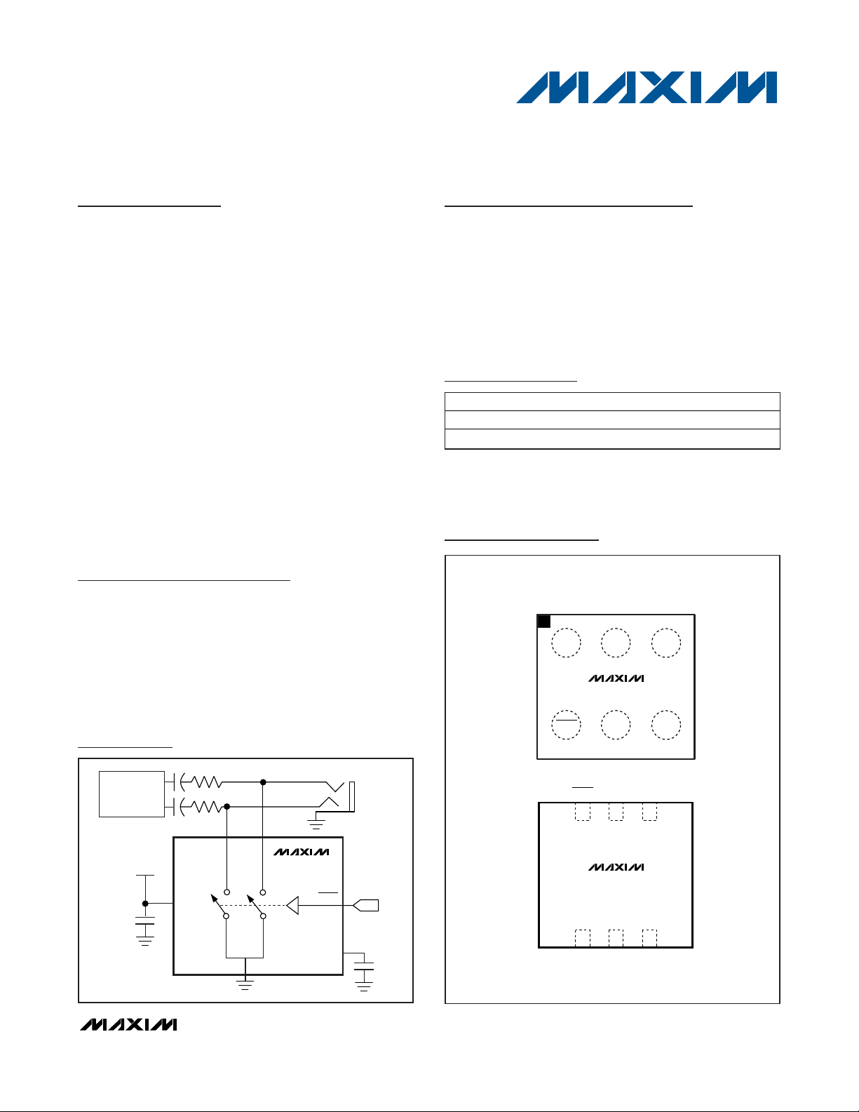
123
A
B
UCSP
TOP VIEW
(BUMPS ON BOTTOM)
INL
GND
INR
V
DD
SET
MUTE
4
3
INL
MUTE
5
2
GND
V
DD
6
1
INR
SET
μDFN
TOP VIEW
MAX9892
MAX9892
+
Pin Configurations
MAX9892
MUTE
SET
C
SET
V
DD
GND
1.7V TO 3.6V
HEADPHONE
AMPLIFIER
INL INR
R
SERIES
R
SERIES
0.1μF
Typical Operating Circuit
Ordering Information
PART TEMP RANGE PIN-PACKAGE
MAX9892ERT+ -40°C to +85°C 6 UCSP
MAX9892ELT+ -40°C to +85°C 6 µDFN
Page 2
MAX9892
Shunt Mode Audio Click-and-Pop Eliminator
2 _______________________________________________________________________________________
ABSOLUTE MAXIMUM RATINGS
ELECTRICAL CHARACTERISTICS
(VDD= 3.0V, V
GND
= 0, TA= T
MIN
to T
MAX
, unless otherwise noted. Typical values are at TA= +25°C.) (Note 1)
Stresses beyond those listed under “Absolute Maximum Ratings” may cause permanent damage to the device. These are stress ratings only, and functional
operation of the device at these or any other conditions beyond those indicated in the operational sections of the specifications is not implied. Exposure to
absolute maximum rating conditions for extended periods may affect device reliability.
VDD, MUTE, SET to GND..........................................-0.3V to +6V
INL, INR to GND.................................(V
DD
- 6V) to (VDD+ 0.3V)
Continuous Current In/Out of V
DD
......................................30mA
Continuous Current In/Out of MUTE ...................................30mA
Continuous Current In/Out of SET.......................................30mA
Continuous Current In/Out of INL, INR and GND .............390mA
Continuous Power Dissipation (T
A
= +70°C)
6-Bump UCSP (derate 3.9mW/°C above +70°C) .....308.3mW
6-Pin µDFN (derate 4.5mW/°C above +70°C) ..........357.8mW
Operating Temperature Range ...........................-40°C to +85°C
Junction Temperature......................................................+150°C
Storage Temperature Range .............................-65°C to +150°C
Lead Temperature (soldering, 10s) .................................+300°C
Bump Temperature (soldering)
Reflow ..........................................................................+235°C
Note 1: All devices are 100% production tested at TA= +25°C. All temperature limits are guaranteed by design.
Note 2: Operating within the recommended supply voltage range ensures that negative audio signals are not limited by the device.
Supply voltages above the recommended supply voltage range may limit the headphone amplifier’s maximum output voltage.
Note 3: Supply current is measured when switches are off.
Supply Voltage Range V
Recommended Supply Voltage
Range
Supply Current I
Input Voltage Range V
Turn-On Time (Figure 1) t
Turn-Off Time (Figure 1) t
Turn-On Time Resistor R
Click-and-Pop Reduction R
Input Leakage Current I
MUTE Leakage Current I
MUTE Input-Voltage High V
MUTE Input-Voltage Low V
PARAMETER SYMBOL CONDITIONS MIN TYP MAX UNITS
Guaranteed by RON test 1.7 5.5 V
(Note 2) 1.7 3.6 V
VDD = 5.5V, TA = +25°C (Note 3) 0.6 1 µA
Guaranteed by input leakage current test
IN
Measured from MUTE = GND and input
voltage settled to 90% of its final value
C
= 500pF 4 10 17
SET
C
= 50pF 1
SET
C
= 50nF 1000
SET
C
= 500pF 350 800 1300 kΩ
SET
V
OFF
DD
DD
DD
ON
SET
VDD = 3.0V 0.3
ON
VDD = 1.7V 2Switch On-Resistance R
VDD = 5.5V 1
= 30Ω, R
SERIES
IN
MUTE
TA = +25°C
VDD = 5.5V, V
IH
IL
V
-
DD
5.5V
V
DD
130 ns
= 16Ω 35 dB
LOAD
VIN = VDD - 5.5V, VDD = 1.7V ±1
V
= VDD, VDD = 5.5V ±1
IN
= 0 or 5.5V, TA = +25°C ±1 µA
MUTE
1.5 V
0.4 V
V
ms
Ω
µA
Page 3
MAX9892
Shunt Mode Audio Click-and-Pop Eliminator
_______________________________________________________________________________________ 3
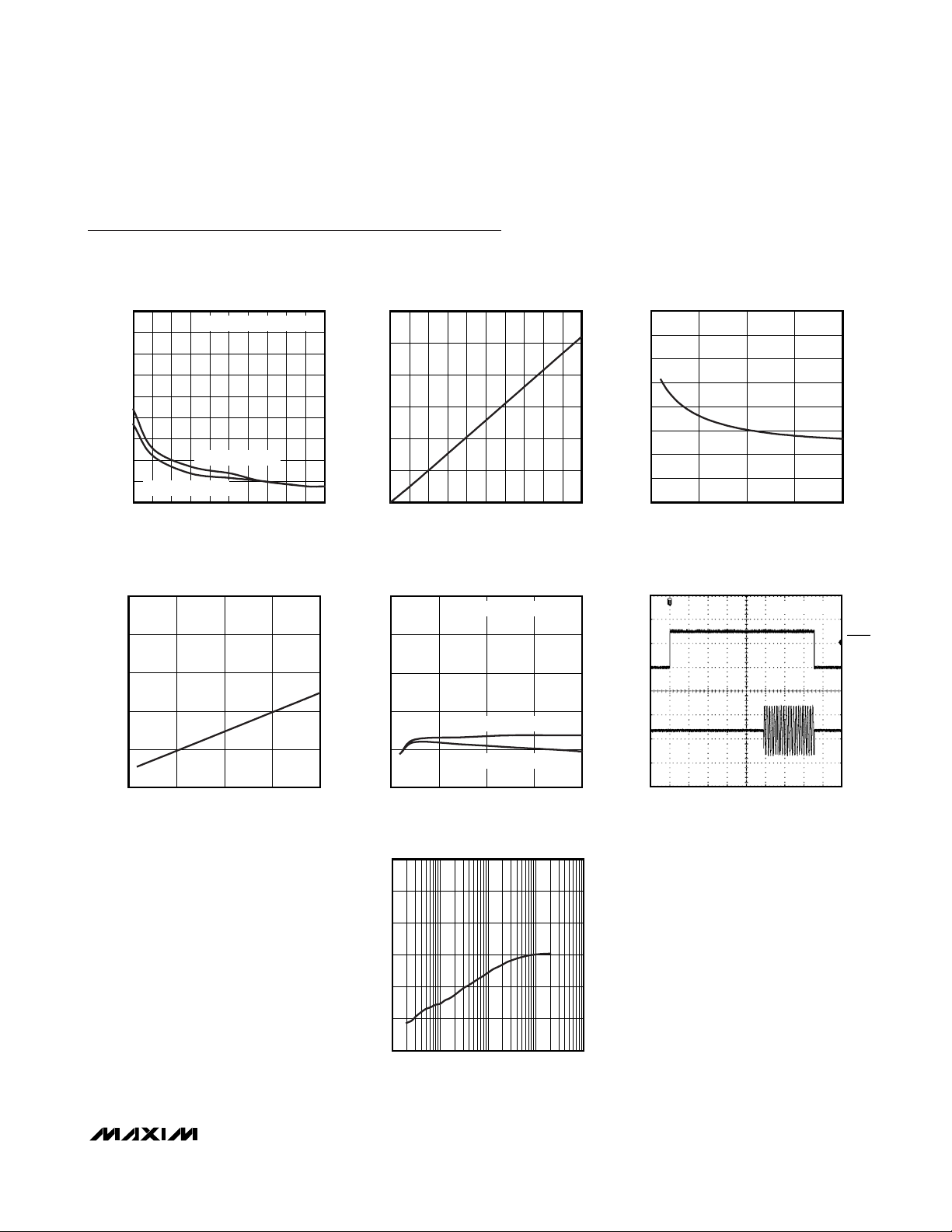
Typical Operating Characteristics
(VDD= 3.0V, V
GND
= 0, TA = +25°C, unless otherwise noted.)
0
-10
-20
-30
-40
-50
-60
CLICK AND POP (dBV)
-70
-80
INTO SHUTDOWN
-90
02010 4030 6050 8070 10090
1.0
0.8
0.6
(μA)
DD
I
0.4
0.2
CLICK AND POP vs. R
TESTED WITH THE MAX4338
OUT OF SHUTDOWN
R
SERIES
SERIES
MAX9892 toc01
(Ω)
SUPPLY CURRENT
vs. SUPPLY VOLTAGE
MAX9892 toc04
t
vs. C
OFF
1200
1000
800
(ms)
600
OFF
t
400
200
0
020155 10 253035404550
CLICK AND POP vs. V
0
-20
-40
-60
CLICK AND POP (dBV)
-80
SET
C
(nF)
SET
TESTED WITH THE MAX4338
OUT OF SHUTDOWN
INTO SHUTDOWN
RON vs. SUPPLY VOLTAGE
0.8
0.7
MAX9892 toc02
0.6
0.5
(Ω)
0.4
ON
R
0.3
0.2
0.1
0
1.5 2.5 3.5 4.5 5.5
VDD (V)
DD
MAX9892 toc05
SWITCH TURN-OFF/ON TIME
C
= 500pF
SET
MAX9892 toc06
MAX9892 toc03
MUTE
2V/div
IN_
2V/div
0
1.5 3.52.5 4.5 5.5
VDD (V)
-100
1.5 3.52.5 4.5 5.5
VDD (V)
CROSSTALK vs. FREQUENCY
0
-20
-40
-60
CROSSTALK (dB)
-80
-100
-120
0.01 100
FREQUENCY (kHz)
2ms/div
MAX9892 toc07
1010.1
Page 4

MAX9892
Shunt Mode Audio Click-and-Pop Eliminator
4 _______________________________________________________________________________________
Pin Description
Timing Diagram
Figure 1. Turn-On/Off Time
UCSP µDFN
BUMP PIN
NAME FUNCTION
A1 1 INL
A2 2 GND Ground
A3 3 INR
B1 6 MUTE Active-Low Enable
B2 5 V
B3 4 SET
MUTE
IN_
Left-Channel Input. Connect INL in between the output coupling capacitor and the headphone
jack.
Right-Channel Input. Connect INR in between the output coupling capacitor and the
headphone jack.
Power Supply
DD
Turn-Off Time Set. Connect an external capacitor in between SET and GND to set the switch
open delay; see the Setting the Turn-Off Time section for more information.
GND
V
DD
GND
VDD - 5.5V
t
R
ON
OFF
t
ON
0.5Ω
Page 5

Detailed Description
The MAX9892 is the second-generation click-and-pop
eliminator designed to be used with conventional headphone amplifiers. The MAX9892 works by adding a lowimpedance current path from the headphone side of
the DC-blocking capacitor to ground. Drive MUTE low
when turning off the amplifier, and high when enabling
the amplifier. A short turn-on time allows the switches in
the MAX9892 to close before the DC-blocking capacitors have significantly discharged, eliminating clicks
and pops at amplifier turn-off. An adjustable turn-off
time allows the delay to be set to mask all clicks and
pops during amplifier turn-on.
Setting the Turn-Off Time
The MAX9892 features a SET input that allows the turnoff time to be adjusted from 1ms to 1000ms to match
the click-and-pop profile of the amplifier startup. The
value of an external capacitor sets the switch open
delay, as shown in the following equation:
tON(ms) = 0.02 x C
SET
(pF)
When the headphone amplifier is enabled, the
MAX9892 automatically waits the set delay time before
opening the analog switches. This allows amplifier turnon click and pop to be eliminated.
Applications Information
Setting the Supply Voltage
The MAX9892 operates from 1.7V to 3.6V supply voltage. The inputs, INL and INR, accept voltage swings
from VDDto VDD- 5.5V. The audio signal applied to a
headphone is ground biased, meaning that the signal
swings just as much negative as positive. Since the
MAX9892 input voltage is limited to VDD- 5.5V on the
negative side, the voltage on VDDmust be set properly
to pass the audio signal when the switch is open
(Figure 2).
A voltage-divider can be used to scale down an available supply voltage as shown in Figure 3. The voltagedivider allows the creation of a supply voltage for the
MAX9892 that is low enough to allow the negative portion of the audio signal to pass. When using large resistances for the voltage-divider, the supply current
affects what resistors to use. Select R2between 10kΩ
to 1MΩ for a given supply voltage. Use the following
equation to calculate the R1:
where V
AMP
is the supply voltage of the amplifier, and
I2is the current through R2. For a signal of ±2V in reference to GND, the MAX9892 supply can be set from 2V
to 3.5V.
Selecting Series Resistors
A series resistor (R
SERIES
), as shown in the
Typical
Operating Circuit
, is necessary to achieve optimal click-
and-pop reduction. See the Click and Pop vs. R
SERIES
graph in the
Typical Operating Characteristics
for
details on how much click-and-pop reduction to expect
for a given series resistor.
Layout Considerations
Bypass VDDto GND with a 0.1µF capacitor. The 0.1µF
bypass capacitor should be positioned as close as
possible to VDD. Minimize trace length from GND to
solid system ground plane to ensure optimum performance.
Refer to the MAX9892 Evaluation Kit for a proven PCB
layout.
MAX9892
Shunt Mode Audio Click-and-Pop Eliminator
_______________________________________________________________________________________ 5
Figure 2. Proper Supply Selected for a Given Input Signal.
A: Supply Voltage with a Large Signal;
B: Supply Voltage with a Small Signal
VV
−
()
AMP DD
R
=
1
II
+
DD
2
A
V
DD
IN_
- 5.5V
V
DD
B
V
DD
IN_
V
- 5.5V
DD
GND
GND
Page 6

MAX9892
UCSP Applications Information
For the latest application details on UCSP construction,
dimensions, tape-carrier information, printed circuit
board techniques, bump-pad layout, and recommended reflow temperature profile, as well as the latest information on reliability testing results, refer to Application
Note 1891:
Understanding the Basics of the Wafer-
Level Chip-Scale Package (WL-CSP)
at www.maxim-
ic.com/ucsp. See Figure 4 for the recommended
MAX9892 PCB footprint.
Shunt Mode Audio Click-and-Pop Eliminator
6 _______________________________________________________________________________________
Figure 3. Scaling Down the Supply Voltage with a Voltage
Divider
Figure 4. PCB Footprint Recommendation Diagram
Chip Information
PROCESS: BiCMOS
HEADPHONE
AMP V
DD
R
1
V
DD
0.1μF
R
2
MAX9892
GND
45±5μm
250μm
Page 7

MAX9892
Shunt Mode Audio Click-and-Pop Eliminator
_______________________________________________________________________________________ 7
Package Information
For the latest package outline information and land patterns, go to www.maxim-ic.com/packages.
PACKAGE TYPE PACKAGE CODE DOCUMENT NO.
6 UCSP R6-1A1+1
21-0228
6 µDFN L622-1
21-0164
UCSP.EPS
Page 8

MAX9892
Shunt Mode Audio Click-and-Pop Eliminator
8 _______________________________________________________________________________________
Package Information (continued)
For the latest package outline information and land patterns, go to www.maxim-ic.com/packages.
D
AAA
AAA
PIN 1
INDEX AREA
SAMPLE
MARKING
7
A1
A
e
b
N
SOLDER
MASK
COVERAGE
6, 8, 10L UDFN.EPS
E
PIN 1
0.10x45∞
L
A A
1
L1
(N/2 -1) x e)
C
L
b
A
A2
L
e
EVEN TERMINAL
C
L
e
ODD TERMINAL
L
PACKAGE OUTLINE,
6, 8, 10L uDFN, 2x2x0.80 mm
21-0164
1
2
B
Page 9

MAX9892
Shunt Mode Audio Click-and-Pop Eliminator
Maxim cannot assume responsibility for use of any circuitry other than circuitry entirely embodied in a Maxim product. No circuit patent licenses are
implied. Maxim reserves the right to change the circuitry and specifications without notice at any time.
Maxim Integrated Products, 120 San Gabriel Drive, Sunnyvale, CA 94086 408-737-7600 _____________________
9
© 2008 Maxim Integrated Products is a registered trademark of Maxim Integrated Products, Inc.
Package Information (continued)
For the latest package outline information and land patterns, go to www.maxim-ic.com/packages.
COMMON DIMENSIONS
-
e b
0.65 BSC
0.40 BSC
MAX.
0.80
2.05
2.05
0.50
0.30±0.05
0.25±0.050.50 BSC8L822-1
0.20±0.03
(N/2 -1) x e
1.30 REF.
1.50 REF.
1.60 REF.
SYMBOL
A
A1
A2
D 1.95 2.00
E
L
L1
PACKAGE VARIATIONS
PKG. CODE
MIN.
0.70 0.75
0.15 0.20 0.25
0.020 0.025 0.035
1.95 2.00
0.30 0.40
0.10 REF.
N
6L622-1
10L1022-1
NOM.
PACKAGE OUTLINE,
6, 8, 10L uDFN, 2x2x0.80 mm
21-0164
2
2
B
 Loading...