

Page 1
General Description
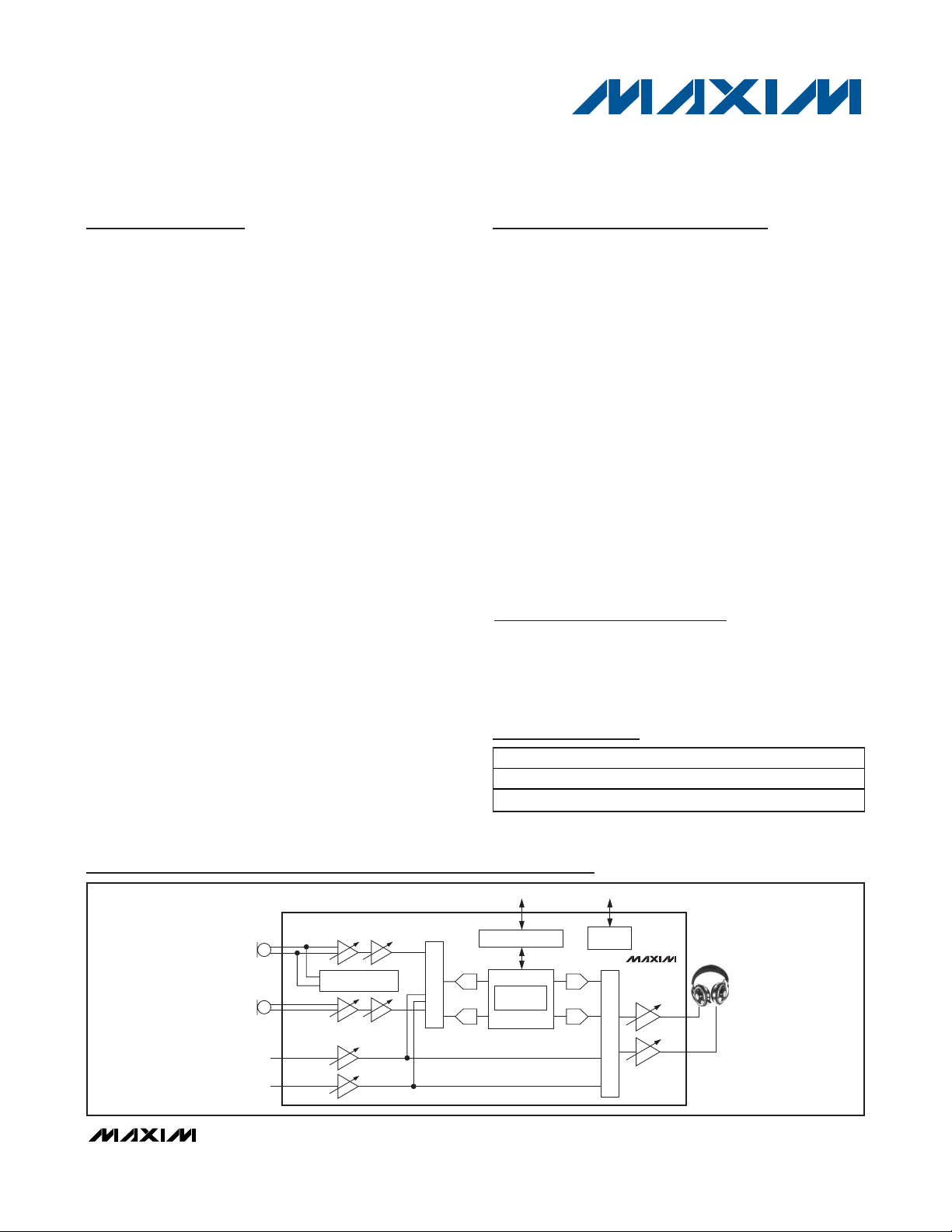
The MAX9867 is an ultra-low power stereo audio codec
designed for portable consumer devices such as
mobile phones and portable gaming consoles.
The device features stereo differential microphone inputs
that can be connected to either analog or digital microphones. The single-ended line inputs, with configurable
preamplifier, can be sent to the ADC for record or routed
directly to the headphone amplifier for playback. An auxiliary ADC path can be used to track any DC voltage.
The stereo headphone amplifiers support differential,
single-ended, and capacitorless output configurations.
Using the capacitorless output configuration, the
device can output 10mW into 32Ω headphones.
Comprehensive click-and-pop circuitry suppresses
audible clicks and pops during volume changes and
startup or shutdown.
Utilizing Maxim’s proprietary digital circuitry, the device
can accept any available 10MHz to 60MHz system
clock. This architecture eliminates the need for an
external PLL and multiple crystal oscillators. The stereo
ADC and DAC paths provide user-configurable voiceband or audioband digital filters. Voiceband filters provide extra attenuation at the GSM packet frequency
and greater than 70dB stopband attenuation at f
S/2
.
The MAX9867 operates from a single 1.8V supply, and
supports a 1.65V to 3.6V logic level. An I
2
C 2-wire serial interface provides control for volume levels, signal
mixing, and general operating modes.
The MAX9867 is available in a tiny 2.2mm x 2.7mm,
0.4mm-ball-pitch, WLP package. A 32-pin 5mm x 5mm
TQFN package is also available.
Features
o 1.8V Single-Supply Operation
o 6.7mW Playback Power Consumption
o 90dB Stereo DAC, 8kHz ≤ fs ≤ 48kHz
o 85dB Stereo ADC, 8kHz ≤ fs ≤ 48kHz
o Battery-Measurement Auxiliary ADC
o Support for Any Master Clock Between 10MHz to
60MHz
o Stereo Digital Microphone Input Support
o Stereo Analog Differential Microphone Inputs
o Stereo Headphone Amplifiers: Differential,
Single-Ended, or Capacitorless
o Stereo Line Inputs
o Voiceband Filter with a Stopband Attenuation
Greater than 70dB
o 1.65V to 3.6V Digital Interface Supply Voltage
o I2S/TDM-Compatible Digital Audio Bus
o 30-Bump, 2.2mm x 2.7mm 0.4mm-Pitch WLP
MAX9867
Ultra-Low Power Stereo Audio Codec
________________________________________________________________
Maxim Integrated Products
1
19-4573; Rev 0; 4/09
For pricing, delivery, and ordering information, please contact Maxim Direct at 1-888-629-4642,
or visit Maxim’s website at www.maxim-ic.com.
Ordering Information
+
Denotes lead(Pb)-free/RoHS-compliant package.
*EP = Exposed pad.
Applications
Cell Phones
Portable Gaming Devices
Portable Navigation Devices
Portable Multimedia Players
Wireless Headsets
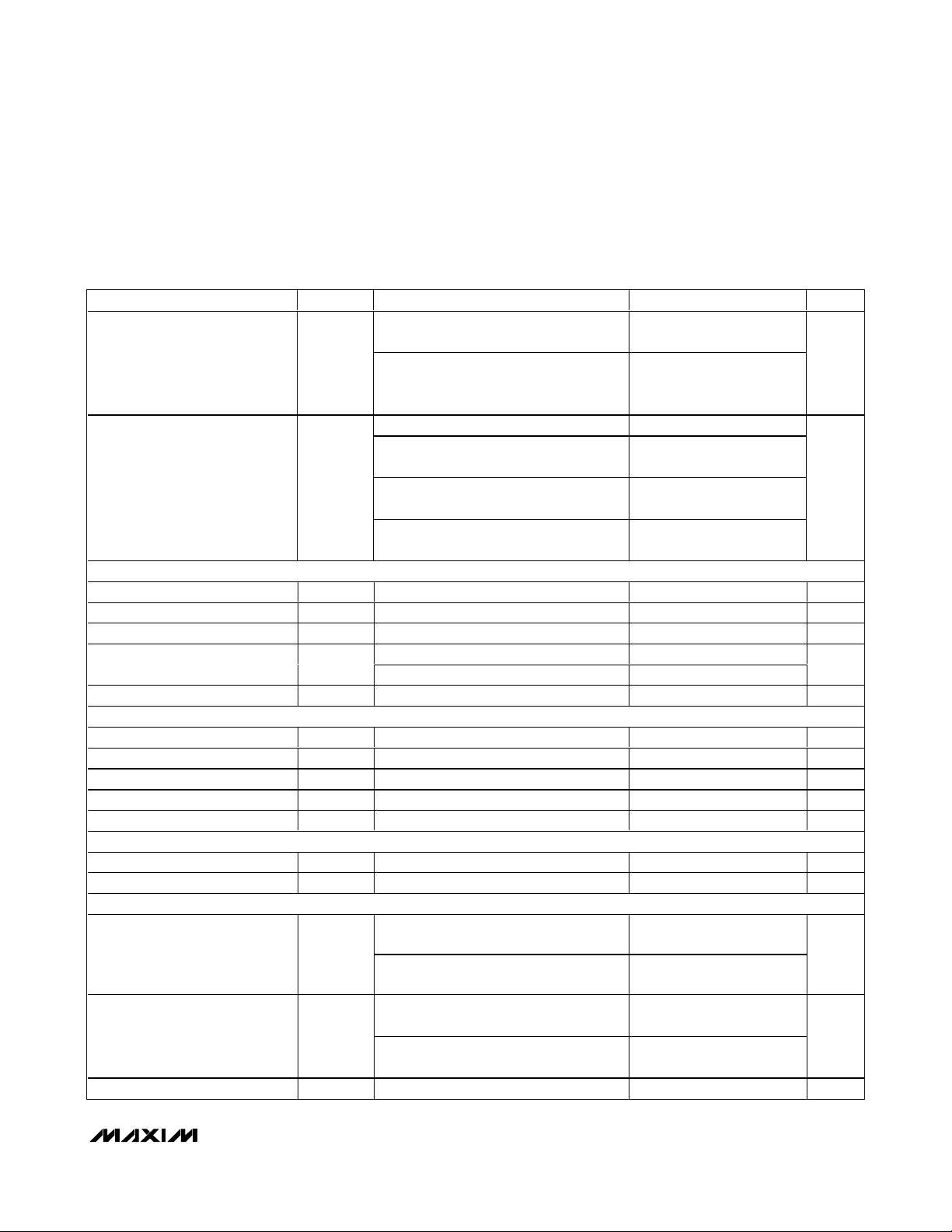
Simplified Block Diagram
PART TEMP RANGE PIN-PACKAGE
MAX9867EWV+ -40°C to +85°C 30 WLP
MAX9867ETJ+ -40°C to +85°C 32 TQFN-EP*
2
CI2S/PCM
I
DAC
DAC
CONTROL
INTERFACE
MIX
MAX9867
HEADPHONE
AMP
HEADPHONE
AMP
LEFT MIC AMP
DIGITAL MICROPHONE
INTERFACE
RIGHT MIC AMP
LINEIN 1
LINEIN 2
LEFT PREAMP
RIGHT PREAMP
MIX
DIGITAL AUDIO INTERFACE
ADC
AUDIO DIGITAL
ADC
FILTERS
Page 2
MAX9867
Ultra-Low Power Stereo Audio Codec
2 _______________________________________________________________________________________
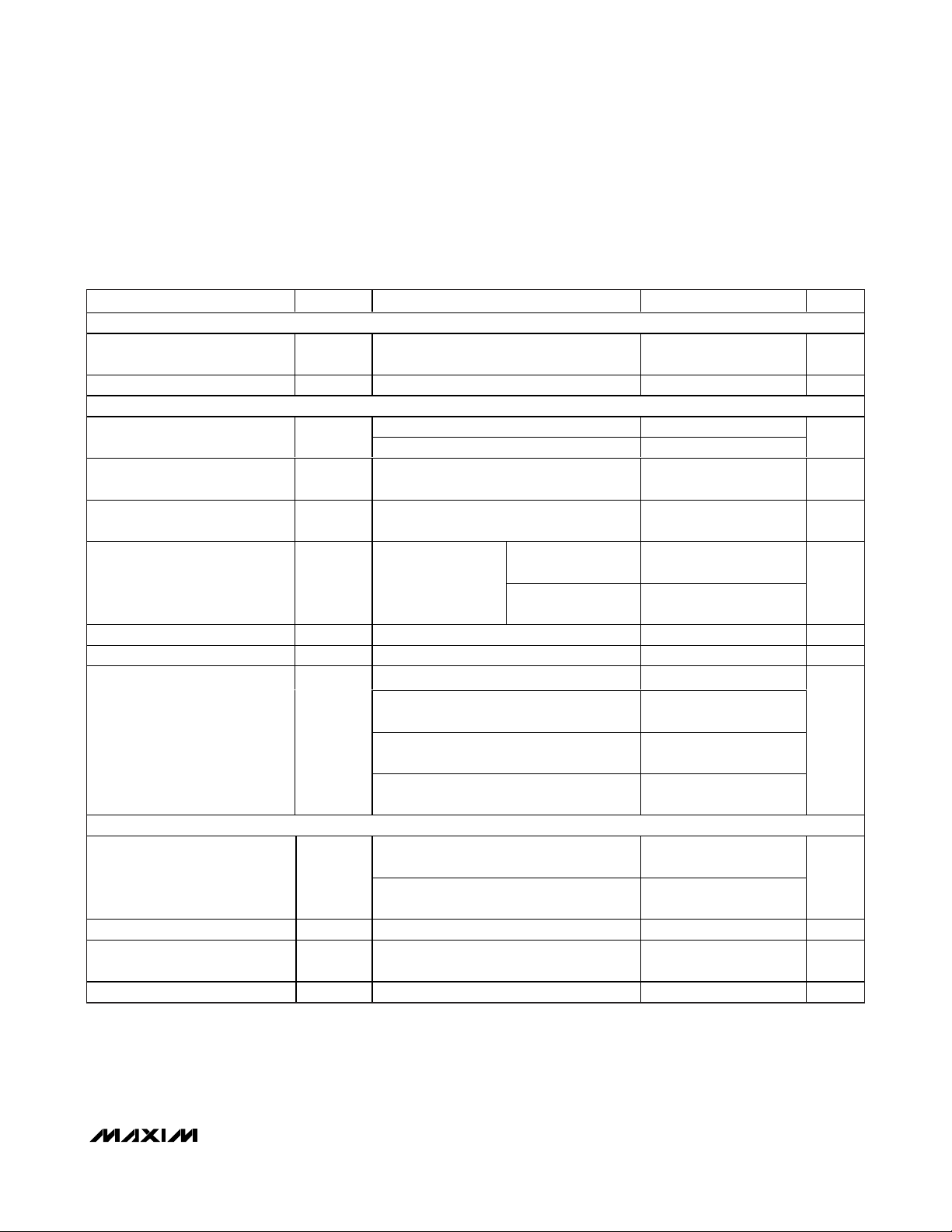
ABSOLUTE MAXIMUM RATINGS
ELECTRICAL CHARACTERISTICS
(V
AVDD
= V
PVDD
= V
DVDD
= V
DVDDIO
= +1.8V, RL= ∞, headphone load (RL) connected between _OUTP and _OUTN in differential
mode, C
REF
= 2.2μF, C
MICBIAS
= C
PREG
= C
REG
= 1μF, AV
PRE
= +20dB, AV
PGAM
= 0dB, AV
DAC
= 0dB, AV
LINE
= +20dB, AV
VOL
=
0dB, MCLK = 13MHz, T
A
= T
MIN
to T
MAX
, unless otherwise noted. Typical values are at TA= +25°C.) (Note 2)
Stresses beyond those listed under “Absolute Maximum Ratings” may cause permanent damage to the device. These are stress ratings only, and functional
operation of the device at these or any other conditions beyond those indicated in the operational sections of the specifications is not implied. Exposure to
absolute maximum rating conditions for extended periods may affect device reliability.
(Voltages with respect to AGND.)
DVDD, AVDD, and PVDD .........................................-0.3V to +2V
DVDDIO.................................................................-0.3V to +3.6V
DGND and PGND..................................................-0.1V to +0.1V
PREG, REF, REG, MICBIAS ....................-0.3V to (AVDD + 0.3V)
MCLK, LRCLK, BCLK
SDOUT, SDIN .................................-0.3V to (DVDDIO + 0.3V)
SDA, SCL, IRQ ......................................................-0.3V to +3.6V
LOUTP, LOUTN, ROUTP,
ROUTN .................................(PGND - 0.3V) to (PVDD + 0.3V)
LINL, LINR, JACKSNS/AUX, MICLP/DIGMICDATA,
MICLN/DIGMICCLK, MICRP, MICRN..-0.3V to (AVDD + 0.3V)
Continuous Power Dissipation (T
A
= +70°C)
30-Bump WLP (derate 12.5mW/°C above +70°C) ....1000mW
32-Pin TQFN-EP (derate 34.5mW/°C above +70°C) .2759mW
Junction-to-Ambient Thermal Resistance (θ
JA
) (Note 1)
30-Bump WLP .............................................................80°C/W
32-Pin TQFN-EP ..........................................................29°C/W
Operating Temp Range.......................................-40°C to +85°C
Storage Temp Range ........................................-65°C to +150°C
Note 1: Package thermal resistances were obtained using the method described in JEDEC specification JESD51-7, using a four-
layer board. For detailed information on package thermal considerations, refer to www.maxim-ic.com/thermal-tutorial
.
Supply Voltage Range
Total Supply Current I
Shutdown Supply Current TA = +25°C
PARAMETER SYMBOL CONDITIONS MIN TYP MAX UNITS
VDD
PVDD, DVDD, AVDD 1.65 1.8 1.95
DVDDIO 1.65 1.8 3.6
Full-duplex 8kHz
mono (voice mode)
(Note 3)
DAC playback 48kHz
stereo (audio mode)
(Note 3)
Full-duplex 48kHz
stereo (audio mode)
(Note 3)
Stereo line-in only
Analog (AVDD +
PVDD)
Digital (DVDD +
DVDDIO)
Analog (AVDD +
PVDD)
Digital (DVDD +
DVDDIO)
Analog (AVDD +
PVDD)
Digital (DVDD +
DVDDIO)
Analog (AVDD +
PVDD)
Digital (DVDD +
DVDDIO)
Analog (AVDD +
PVDD)
Digital (DVDD +
DVDDIO)
4.65 7
0.96 1.5
3.28 5
1.40 2
8.0 12
2.0 3
3.8 6
0.004 0.05
15
15
V
mA
μA
Page 3
MAX9867
Ultra-Low Power Stereo Audio Codec
_______________________________________________________________________________________ 3
ELECTRICAL CHARACTERISTICS (continued)
(V
AVDD
= V
PVDD
= V
DVDD
= V
DVDDIO
= +1.8V, RL= ∞, headphone load (RL) connected between _OUTP and _OUTN in differential
mode, C
REF
= 2.2μF, C
MICBIAS
= C
PREG
= C
REG
= 1μF, AV
PRE
= +20dB, AV
PGAM
= 0dB, AV
DAC
= 0dB, AV
LINE
= +20dB, AV
VOL
=
0dB, MCLK = 13MHz, T
A
= T
MIN
to T
MAX
, unless otherwise noted. Typical values are at TA= +25°C.) (Note 2)
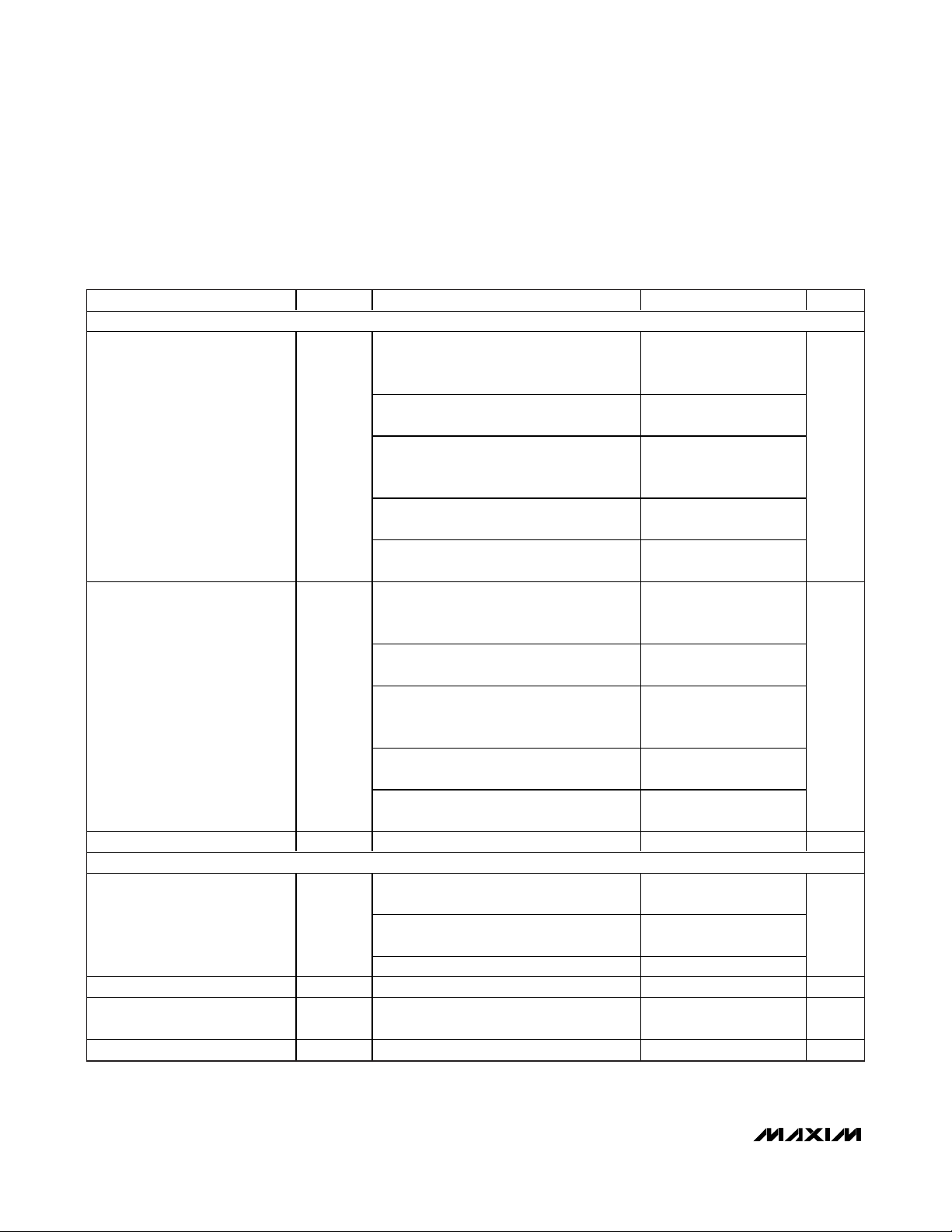
PARAMETER SYMBOL CONDITIONS MIN TYP MAX UNITS
Shutdown to Full Operation Excludes PLL lock time 10 ms
Soft-Start/-Stop Time 10 ms
DAC (Note 4)
Dynamic Range (Note 5) DR
f
= 48kHz, AV
S
+0dB, T
A
VOL
= +25°C
Master or slave
=
mode
Slave mode 84
90
Differential mode 1
Full-Scale Output V
Gain Error
Voice Path Phase Delay P
DLY
Total Harmonic Distortion THD
DAC Attenuation Range AV
DAC Gain Adjust AV
DAC
GAIN
Power-Supply Rejection Ratio PSRR
OLL/VOLR
DC accuracy, measured with respect to
full-scale output
f = 1kH z, 0d BFS , H P
fi l ter d i sab l ed , d i g i tal
i np ut to anal og outp ut
MCLK = 12.288MHz, f
measured at headphone outputs
DACA = 0xF to 0x0 -15 0 dB
DACG = 00 to 11 0 +18 dB
V
AVDD
f = 217Hz, V
AV
f = 1kHz, V
AV
f = 10kHz, V
AV
VOL
VOL
VOL
= 0 x 09
= V
PVDD
= 0dB
RIPPLE
= 0dB
= 0dB
Capacitorless and
single-ended modes
fS = 8kHz 1.2
= 16kHz 0.59
f
S
= 48kHz, 0dBFS,
S
= 1.65V to 1.95V 60 78
RIPPLE
RIPPLE
= 100mV
= 100mV
= 100mV
P-P
P-P
P-P
,
,
,
0.56
15%
-80 dB
78
75
62
DAC VOICE MODE DIGITAL IIR LOWPASS FILTER
With respect to fS within ripple; fS = 8kHz to
Passband Cutoff f
PLP
48kHz
-3dB cutoff
Passband Ripple f < f
Stopband Cutoff f
SLP
With respect to fS; fS = 8kHz to 48kHz
Stopband Attenuation f > f
PLP
, f = 20Hz to 20kHz 75 dB
SLP
0.448 x
f
S
0.451 x
f
S
±0.1 dB
0.476 x
f
S
V
dB
RMS
ms
dB
Hz
Hz
Page 4
MAX9867
Ultra-Low Power Stereo Audio Codec
4 _______________________________________________________________________________________
ELECTRICAL CHARACTERISTICS (continued)
(V
AVDD
= V
PVDD
= V
DVDD
= V
DVDDIO
= +1.8V, RL= ∞, headphone load (RL) connected between _OUTP and _OUTN in differential
mode, C
REF
= 2.2μF, C
MICBIAS
= C
PREG
= C
REG
= 1μF, AV
PRE
= +20dB, AV
PGAM
= 0dB, AV
DAC
= 0dB, AV
LINE
= +20dB, AV
VOL
=
0dB, MCLK = 13MHz, T
A
= T
MIN
to T
MAX
, unless otherwise noted. Typical values are at TA= +25°C.) (Note 2)
PARAMETER SYMBOL CONDITIONS MIN TYP MAX UNITS
DAC VOICE MODE DIGITAL 5th ORDER IIR HIGHPASS FILTER
DVFLT = 0x1
(elliptical tuned for 16kHz GSM + 217Hz
notch)
0.0161
x f
S
5th Order Passband Cutoff
(-3dB from Peak, I
2
C Register
Programmable)
5th Order Stopband Cutoff
(-30dB from Peak, I
2
C Register
Programmable)
DC Attenuation DC
f
DHPPB
f
DHPSB
ATTEN
DVFLT = 0x2
(500Hz Butterworth tuned for 16kHz)
DVFLT = 0x3
(elliptical tuned for 8kHz GSM + 217Hz
notch)
DVFLT = 0x4
(500Hz Butterworth tuned for 8kHz)
DVFLT = 0x5
/240 Butterworth)
(f
S
DVFLT = 0x1
(elliptical tuned for 16kHz GSM + 217Hz
notch)
DVFLT = 0x2
(500Hz Butterworth tuned for 16kHz)
DVFLT = 0x3
(elliptical tuned for 8kHz GSM + 217Hz
notch)
DVFLT = 0x4
(500Hz Butterworth tuned for 8kHz)
DVFLT = 0x5
/240 Butterworth)
(f
S
DVFLT ≠ 000 90 dB
0.0312
x f
S
0.0321
x f
S
0.0625
x f
S
0.0042
x f
S
0.0139
x f
S
0.0156
x f
S
0.0279
x f
S
0.0312
x f
S
0.0021
x f
S
Hz
Hz
DAC STEREO AUDIO MODE DIGITAL FIR LOWPASS FILTER
With respect to fS within ripple;
= 8kHz to 48kHz
f
S
Passband Cutoff f
PLP
-3dB cutoff
-6.02dB cutoff
Passband Ripple f < f
Stopband Cutoff f
SLP
With respect to fS; fS = 8kHz to 48kHz
PLP
0.43 x
f
S
0.47 x
f
S
0.50 x
f
S
±0.1 dB
0.58 x
f
S
Hz
Hz
Stopband Attenuation 60 dB
Page 5
MAX9867
Ultra-Low Power Stereo Audio Codec
_______________________________________________________________________________________ 5
ELECTRICAL CHARACTERISTICS (continued)
(V
AVDD
= V
PVDD
= V
DVDD
= V
DVDDIO
= +1.8V, RL= ∞, headphone load (RL) connected between _OUTP and _OUTN in differential
mode, C
REF
= 2.2μF, C
MICBIAS
= C
PREG
= C
REG
= 1μF, AV
PRE
= +20dB, AV
PGAM
= 0dB, AV
DAC
= 0dB, AV
LINE
= +20dB, AV
VOL
=
0dB, MCLK = 13MHz, T
A
= T
MIN
to T
MAX
, unless otherwise noted. Typical values are at TA= +25°C.) (Note 2)
PARAMETER SYMBOL CONDITIONS MIN TYP MAX UNITS
DAC STEREO AUDIO MODE DIGITAL DC BLOCKING HIGHPASS FILTER
Passband Cutoff
(-3dB from Peak)
DC Attenuation DC
f
DHPPB
ATTEN
DVFLT = 0x1
DVFLT = 0x1 90 dB
0.000625
x f
S
ADC (Note 6)
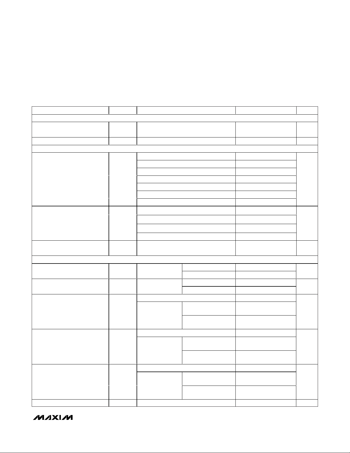
Dynamic Range (Note 5) DR
Full-Scale Input
Gain Error (Note 7)
Voice Path Phase Delay P
DLY
fS = 8kHz, MODE = 0 (IIR voice) 75 84
= 8kHz to 48kHz, MODE = 1 (FIR audio) 85
f
S
Differential MIC input or stereo-line inputs,
AVPRE = 0dB, AVPGA = 0dB
DC accuracy, measured with respect to
80% of full-scale output
f = 1kHz, 0dBFS, HP
fS = 8kHz 1.2
filter disabled,
analog input to
digital output
f
= 16kHz 0.61
S
1V
15%
Total Harmonic Distortion THD f = 1kHz, fS = 8kHz, TA = +25°C, 0dBFs -81 -70 dB
ADC Level Adjust Range AV
ADC
Power-Supply Rejection Ratio PSRR
AVL/VR = 0xF to 0x0 -12 +3 dB
V
= 1.65V to 1.95V, input referred 60 85
AVDD
f = 217Hz, V
input referred
f = 1kHz, V
input referred
f = 10kHz, V
input referred
RIPPLE
RIPPLE
RIPPLE
= 100mV, AV
= 100mV, AV
= 100mV, AV
ADC
ADC
ADC
= 0dB,
= 0dB,
= 0dB,
85
80
80
ADC VOICE MODE DIGITAL IIR LOWPASS FILTER
With respect to fS within ripple;
f
= 8kHz to 48kHz
Passband Cutoff f
PLP
S
-3dB cutoff
Passband Ripple f < f
Stopband Cutoff f
SLP
With respect to fS; fS = 8kHz to 48kHz
Stopband Attenuation f > f
PLP
, f = 20Hz to 20kHz 74 dB
SLP
0.445 x
f
S
0.449 x
f
S
±0.1 dB
0.469 x
f
S
Hz
dB
P-P
ms
dB
Hz
Hz
Page 6
MAX9867
Ultra-Low Power Stereo Audio Codec
6 _______________________________________________________________________________________
ELECTRICAL CHARACTERISTICS (continued)
(V
AVDD
= V
PVDD
= V
DVDD
= V
DVDDIO
= +1.8V, RL= ∞, headphone load (RL) connected between _OUTP and _OUTN in differential
mode, C
REF
= 2.2μF, C
MICBIAS
= C
PREG
= C
REG
= 1μF, AV
PRE
= +20dB, AV
PGAM
= 0dB, AV
DAC
= 0dB, AV
LINE
= +20dB, AV
VOL
=
0dB, MCLK = 13MHz, T
A
= T
MIN
to T
MAX
, unless otherwise noted. Typical values are at TA= +25°C.) (Note 2)
PARAMETER SYMBOL CONDITIONS MIN TYP MAX UNITS
ADC VOICE MODE DIGITAL 5th ORDER IIR HIGHPASS FILTER
AVFLT = 0x1
(elliptical tuned for 16kHz GSM + 217Hz
notch)
0.0161
x f
S
AVFLT = 0x2
(500Hz Butterworth tuned for 16kHz)
5th Order Passband Cutoff
(-3dB from Peak, I
2
C Register
Programmable)
f
AHPPB
AVFLT = 0x3
(elliptical tuned for 8kHz GSM + 217Hz
notch)
AVFLT = 0x4
(500Hz Butterworth tuned for 8kHz)
AVFLT = 0x5
/240 Butterworth)
(f
S
AVFLT = 0x1
(elliptical tuned for 16kHz GSM + 217Hz
notch)
AVFLT = 0x2
(500Hz Butterworth tuned for 16kHz)
Stopband Cutoff (-30dB from
Peak)
f
AHPSB
AVFLT = 0x3
(elliptical tuned for 8kHz GSM + 217Hz
notch)
AVFLT = 0x4
(500Hz Butterworth tuned for 8kHz)
AVFLT = 0x5
/240 Butterworth)
(f
S
DC Attenuation DC
ATTEN
AVFLT ≠ 000 90 dB
ADC STEREO AUDIO MODE DIGITAL FIR LOWPASS FILTER
With respect to fS within ripple;
= 8kHz to 48kHz
f
S
Passband Cutoff f
PLP
-3dB cutoff
-6.02dB cutoff 0.5 x f
Passband Ripple f < f
Stopband Cutoff f
SLP
Stopband Attenuation f > f
PLP
With respect to fS; fS = 8kHz to 48kHz
, f = 20Hz to 20kHz 60 dB
SLP
0.0312
x f
S
0.0321
x f
S
0.0625
x f
S
0.0042
x f
S
0.0139
x f
S
0.0156
x f
S
0.0279
x f
S
0.0312
x f
S
0.0021
x f
S
0.43 x
f
S
0.48 x
f
S
S
±0.1 dB
0.58 x
f
S
Hz
Hz
Hz
Hz
Page 7
MAX9867
Ultra-Low Power Stereo Audio Codec
_______________________________________________________________________________________ 7
ELECTRICAL CHARACTERISTICS (continued)
(V
AVDD
= V
PVDD
= V
DVDD
= V
DVDDIO
= +1.8V, RL= ∞, headphone load (RL) connected between _OUTP and _OUTN in differential
mode, C
REF
= 2.2μF, C
MICBIAS
= C
PREG
= C
REG
= 1μF, AV
PRE
= +20dB, AV
PGAM
= 0dB, AV
DAC
= 0dB, AV
LINE
= +20dB, AV
VOL
=
0dB, MCLK = 13MHz, T
A
= T
MIN
to T
MAX
, unless otherwise noted. Typical values are at TA= +25°C.) (Note 2)
PARAMETER SYMBOL CONDITIONS MIN TYP MAX UNITS
ADC STEREO AUDIO MODE DIGITAL DC BLOCKING HIGHPASS FILTER
Passband Cutoff
(-3dB from Peak)
DC Attenuation DC
f
AHPPB
ATTEN
AVFLT = 0x1
AVFLT = 0x1 90 dB
OUTPUT VOLUME CONTROL
VOLL/VOLR = 0x00 14.55 14.9 15.15
VOLL/VOLR = 0x01 14.1 14.4 14.6
VOLL/VOLR = 0x02 13.6 13.9 14.1
Line Input to Output Volume
Control
AV
VOL
VOLL/VOLR = 0x04 12.6 12.9 13.1
VOLL/VOLR = 0x08 9.35 9.9 10.35
VOLL/VOLR = 0x10 0.35 0.9 1.35
VOLL/VOLR = 0x20 -50.15 -49.2 -48.15
VOLL/VOLR = 0x00 to 0x06 (+6dB to +3dB) 0.5
Output Volume Control Step Size
VOLL/VOLR = 0x06 to 0x0F (+3dB to -6dB) 1
VOLL/VOLR = 0x0F to 0x17 (-6dB to -22dB) 2
V O LL/V O LR = 0x17 to 0x3F ( - 22d B to m ute) 4
Output Volume Control Mute
Attenuation
f = 1kHz 100 dB
HEADPHONE AMPLIFIER (Note 8)
Output Power per Channel
(Differential Mode)
Output Power per Channel
(Capacitorless Mode)
Total Harmonic Distortion + Noise
(Differential Mode)
Total Harmonic Distortion + Noise
(Capacitorless Mode)
Total Harmonic Distortion + Noise
(SE Mode)
P
OUT
P
OUT
THD+N
THD+N
THD+N
Dynamic Range DR AV
f = 1kHz, THD <
1%, T
= +25°C
A
f = 1kHz, THD <
1%, T
= +25°C
A
RL = 16Ω, P
R
= 32Ω, P
L
= 25mW, f = 1kHz -76
OUT
=
OUT
25mW, f = 1kHz
RL = 16Ω, P
R
= 32Ω, P
L
= 6.25mW, f = 1kHz -72
OUT
=
OUT
6.25mW, f = 1kHz
RL = 16Ω, P
R
= 32Ω, P
L
= 6.25mW, f = 1kHz -74
OUT
=
OUT
6.25mW, f = 1kHz
= +6dB (Notes 5, 7) 76 90 dB
VOL
0.000625
x f
S
RL = 16Ω 30 52
R
= 32Ω 32
L
RL = 16Ω 19
R
= 32Ω 810
L
MCLK = 13MHz,
= 8kHz
f
S
MCLK = 12.288MHz,
= 48kHz
f
S
MCLK = 13MHz,
= 8kHz
f
S
MCLK = 12.288MHz,
= 48kHz
f
S
MCLK = 13MHz,
= 8kHz
f
S
MCLK = 12.288MHz,
f
= 48kHz
S
-77 -70
-80
-74 -65
-74
-74 -65
-76
Hz
dB
dB
mW
mW
dB
dB
dB
Page 8
MAX9867
Ultra-Low Power Stereo Audio Codec
8 _______________________________________________________________________________________
ELECTRICAL CHARACTERISTICS (continued)
(V
AVDD
= V
PVDD
= V
DVDD
= V
DVDDIO
= +1.8V, RL= ∞, headphone load (RL) connected between _OUTP and _OUTN in differential
mode, C
REF
= 2.2μF, C
MICBIAS
= C
PREG
= C
REG
= 1μF, AV
PRE
= +20dB, AV
PGAM
= 0dB, AV
DAC
= 0dB, AV
LINE
= +20dB, AV
VOL
=
0dB, MCLK = 13MHz, T
A
= T
MIN
to T
MAX
, unless otherwise noted. Typical values are at TA= +25°C.) (Note 2)
PARAMETER SYMBOL CONDITIONS MIN TYP MAX UNITS
V
= V
AVDD
f = 217Hz, V
= 0dB
AV
Power-Supply Rejection Ratio
(Note 7)
PSRR
VOL
f = 1kHz, V
= 0dB
AV
VOL
f = 10kHz, V
AV
= 0dB
VOL
AV
= -84dB
VOL
differential mode
Output Offset Voltage V
OS
AV
VOL
= -84dB
capacitorless
mode
Differential mode, P
Capacitorless
Crosstalk X
TALK
mode,
P
OUT
= 5mW,
f = 1kHz
Capacitive Drive
Click-and-Pop Level
(Differential, Capacitorless
Modes)
No sustained
oscillations
Peak voltage,
A-weighted, 32
samples per
second
Peak voltage,
Click-and-Pop Level
(SE Mode)
A-weighted, 32
samples per
second
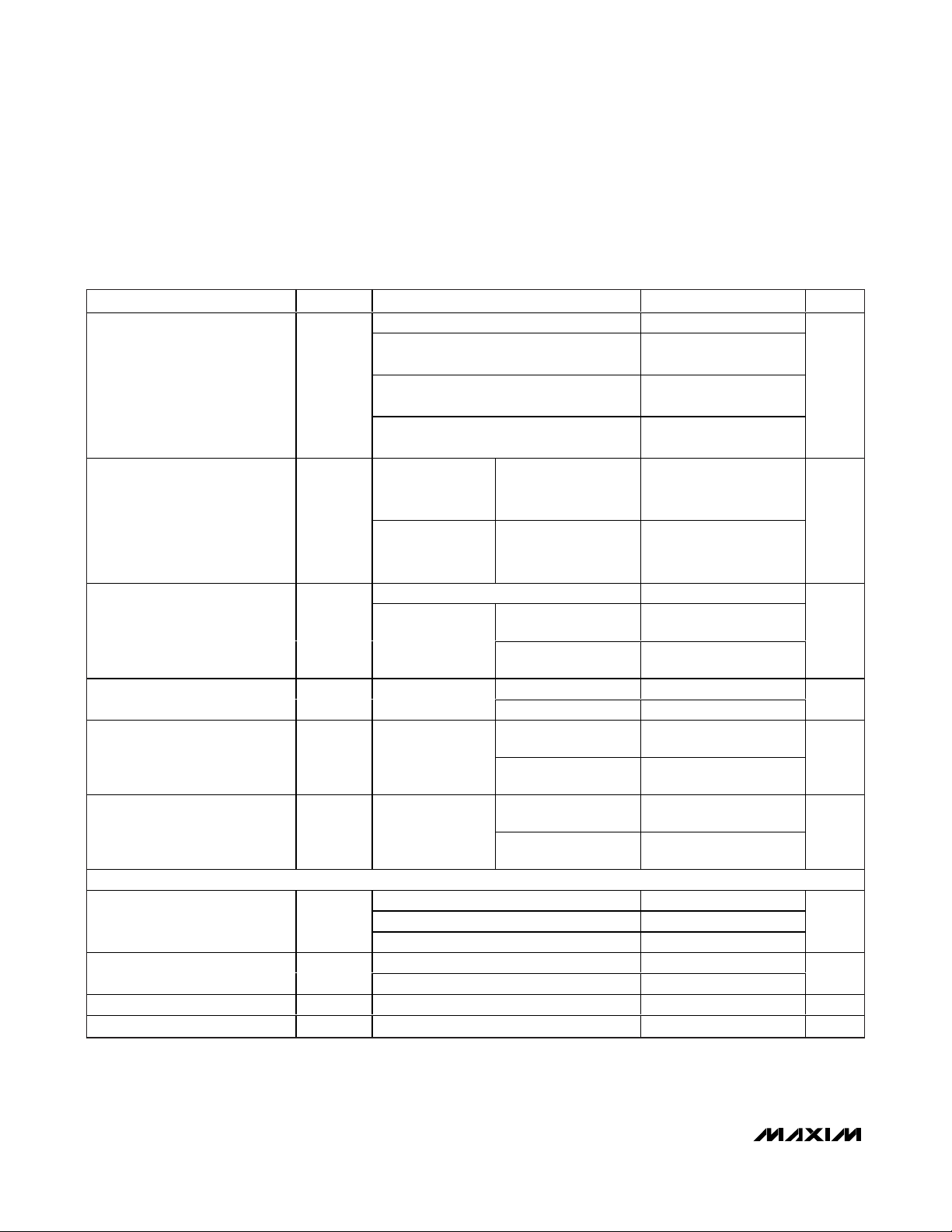
MICROPHONE AMPLIFIER
PALEN/PAREN = 01 -0.5 0 +0.5
Preamplifier Gain AV
PALEN/PAREN = 10 19.5 20 20.5
PRE
PALEN/PAREN = 11 29.5 30 30.5
MIC PGA Gain AV
PGAM
PGAML/PGAMR = 0x1F -0.6 -0.1 +0.4
PGAML/PGAMR = 0x00 19.3 19.75 20.3
Common-Mode Rejection Ratio CMRR VIN = 100mV
MIC Input Resistance R
IN_MIC
All gain settings 30 50 kΩ
= 1.65V to 1.95V 60 78
PVDD
= 100mV
RIPPLE
= 100mV
RIPPLE
= 100mV
RIPPLE
P-P
,
P-P
P-P
,
,
(LOUTP–LOUTN,
ROUTP–ROUTN),
T
= +25°C
A
(LOUTP–LOUTN,
ROUTP–LOUTN),
T
= +25°C
A
= 5mW, f = 1kHz 87
OUT
TQFN 55
WLP 60
RL = 32Ω 500
R
= ∞ 100
L
Into shutdown -80
Out of shutdown -69
Into shutdown -75
Out of shutdown -75
, f = 217Hz 50 dB
P-P
78
75
62
±0.2 ±1.3
±0.8 ±3
dB
mV
dB
pF
dBV
dBV
dB
dB
Page 9
MAX9867
Ultra-Low Power Stereo Audio Codec
_______________________________________________________________________________________ 9
ELECTRICAL CHARACTERISTICS (continued)
(V
AVDD
= V
PVDD
= V
DVDD
= V
DVDDIO
= +1.8V, RL= ∞, headphone load (RL) connected between _OUTP and _OUTN in differential
mode, C
REF
= 2.2μF, C
MICBIAS
= C
PREG
= C
REG
= 1μF, AV
PRE
= +20dB, AV
PGAM
= 0dB, AV
DAC
= 0dB, AV
LINE
= +20dB, AV
VOL
=
0dB, MCLK = 13MHz, T
A
= T
MIN
to T
MAX
, unless otherwise noted. Typical values are at TA= +25°C.) (Note 2)
PARAMETER SYMBOL CONDITIONS MIN TYP MAX UNITS
AV
= 0dB,
Total Harmonic Distortion + Noise THD+N
Power-Supply Rejection Ratio PSRR
PRE
V
= 1V
IN
AV
PRE
V
= 32mV
IN
(1V
P-P
V
AVDD
f = 217Hz, V
AV
ADC
f = 1kHz, V
AV
ADC
f = 10kHz, V
AV
ADC
, f = 1kHz
P-P
= +30dB,
, f = 1kHz,
P-P
at ADC input)
= 1.65V to 1.95V, input referred 60 85
= 100mV,
RIPPLE
= 0dB, input referred
= 100mV,
RIPPLE
= 0dB, input referred
= 100mV,
RIPPLE
= 0dB, input referred
-80
-67
85
80
80
MICROPHONE BIAS
Output Voltage V
MICBIASVAVDD
Load Regulation I
Line Regulation V
Power-Supply Rejection Ratio PSRR
= 1.8V, I
= 1mA to 2mA 0.2 10 V/A
LOAD
= 1.65V to 1.95V 10 μV/V
AVDD
f = 217Hz, V
f = 10kHz, V
RIPPLE
RIPPLE
= 1mA 1.5 1.525 1.55 V
LOAD
= 100mV
= 100mV
P-P
P-P
85
81
Noise Voltage A-weighted 9.1 μV
LINE INPUT
Full-Scale Input V
Line Input Level Adjust Range AV
LINE
AV
IN
= 0dB 1.0 V
LINE
LIGL/LIGR = 0xF to 0x0 -6.5 +24.5 dB
Line Input Mute Attenuation f = 1kHz 100 dB
Input Resistance R
IN_LINE
Total Harmonic Distortion + Noise THD+N VIN = 0.1V
AV
= +24dB 20 kΩ
LINE
, f = 1kHz, differential output -83 dB
P-P
AUXIN INPUT
Input DC Voltage Range AUXEN = 1 0 0.738 V
AUXIN Input Resistance RIN AUXEN = 1, 0V ≤ AUXIN ≤ 0.738 10 40 MΩ
JACK SENSE OPERATION
Threshold VTH
JDETEN = 1, SHDN = 1, JACKSNS
JDETEN = 1, SHDN = 0, JACKSNS,
LOUTP
JDETEN = 1, SHDN = 1,
JACKSNS = GND
0.92 x
MICBIAS
AVDD -
0.8
0.95 x
MICBIAS
AVDD -
0.4
4
0.98 x
MICBIAS
AVDD -
0.15
Pullup Current IPU
JDETEN = 1, SHDN = 0,
JACKSNS = LOUTP = GND
420
Pullup Voltage JDETEN = 1, JACKSNS, LOUTP AVDD V
dB
dB
dB
RMS
P-P
V
μA
Page 10
MAX9867
Ultra-Low Power Stereo Audio Codec
10 ______________________________________________________________________________________
ELECTRICAL CHARACTERISTICS (continued)
(V
AVDD
= V
PVDD
= V
DVDD
= V
DVDDIO
= +1.8V, RL= ∞, headphone load (RL) connected between _OUTP and _OUTN in differential
mode, C
REF
= 2.2μF, C
MICBIAS
= C
PREG
= C
REG
= 1μF, AV
PRE
= +20dB, AV
PGAM
= 0dB, AV
DAC
= 0dB, AV
LINE
= +20dB, AV
VOL
=
0dB, MCLK = 13MHz, T
A
= T
MIN
to T
MAX
, unless otherwise noted. Typical values are at TA= +25°C.) (Note 2)
PARAMETER SYMBOL CONDITIONS MIN TYP MAX UNITS
DIGITAL SIDETONE
Sidetone Gain Adjust Range AV
Voice Path Phase Delay P
STGA
DLY
Differential output mode,
DVST = 0x1F to 0x01
MIC input to headphone output, f = 1kHz,
HP filter disabled, f
= 8kHz
S
-60 0 dB
2.2 ms
INPUT CLOCK CHARACTERISTICS
MCLK Input Frequency f
MCLK Input Duty Cycle
Maximum MCLK Input Jitter
MCLK
For any LRCLK sample rate 10 60 MHz
Prescaler = /1 mode 40 60
/2 or /4 modes 30 70
Maximum allowable RMS for performance
limits
100 ps
LRCLK Sample Rate Range 8 48 kHz
Rapid lock mode 2 7
Nonrapid lock
mode
12 25
LRCLK PLL Lock Time
LRCLK Acceptable Jitter for
Maintaining PLL Lock
Any allowable LRCLK
and PCLK rate, slave
mode
Allowable LRCLK period change from
nominal for slave PLL mode at any
allowable LRCLK and PCLK rates
FREQ = 0x8 through 0xF 0 0 %
LRCLK Average Frequency Error
(Master and Slave Modes)
(Note 9)
PCLK = 192xfS, 256xfS, 384xfS, 512xfS,
768xf
, and 1024xf
S
S
00
All other modes -0.025 +0.025
DIGITAL INPUT (MCLK)
Input High Voltage V
Input Low Voltage V
Input Leakage Current IIH, I
IH
IL
TA = +25°C ±1 μA
IL
1.2 V
Input Capacitance 10 pF
DIGITAL INPUTS (SDIN, BCLK, LRCLK)
Input High Voltage V
Input Low Voltage V
IH
IL
0.7 x
DVDDIO
0.3 x
DVDDIO
Input Hysteresis 200 mV
Input Leakage Current IIH, I
TA = +25°C ±1 μA
IL
Input Capacitance 10 pF
%
ms
±100 ns
0.6 V
RMS
V
V
Page 11
MAX9867
Ultra-Low Power Stereo Audio Codec
______________________________________________________________________________________ 11
ELECTRICAL CHARACTERISTICS (continued)
(V
AVDD
= V
PVDD
= V
DVDD
= V
DVDDIO
= +1.8V, RL= ∞, headphone load (RL) connected between _OUTP and _OUTN in differential
mode, C
REF
= 2.2μF, C
MICBIAS
= C
PREG
= C
REG
= 1μF, AV
PRE
= +20dB, AV
PGAM
= 0dB, AV
DAC
= 0dB, AV
LINE
= +20dB, AV
VOL
=
0dB, MCLK = 13MHz, T
A
= T
MIN
to T
MAX
, unless otherwise noted. Typical values are at TA= +25°C.) (Note 2)
PARAMETER SYMBOL CONDITIONS MIN TYP MAX UNITS
DIGITAL INPUTS (SDA, SCL)
Input High Voltage V
Input Low Voltage V
IH
IL
0.7 x
DVDD
0.3 x
DVDD
Input Hysteresis 200 mV
Input Leakage Current IIH, I
TA = +25°C ±1 μA
IL
Input Capacitance 10 pF
DIGITAL INPUT (DIGMICDATA)
Input High Voltage V
Input Low Voltage V
IH
IL
0.65 x
DVDD
0.35 x
DVDD
Input Hysteresis 100 mV
Input Leakage Current IIH, I
TA = +25°C ±35 μA
IL
Input Capacitance 10 pF
CMOS DIGITAL OUTPUTS (BCLK, LRCLK, SDOUT)
Output Low Voltage V
Output High Voltage V
OL
OH
IOL = 3mA 0.4 V
IOH = 3mA
DVDDIO
- 0.4
CMOS DIGITAL OUTPUT (DIGMICCLK)
Output Low Voltage V
Output High Voltage V
OL
OH
IOL = 1mA 0.4 V
IOH = 1mA
DVDD -
0.4
OPEN-DRAIN DIGITAL OUTPUTS (SDA, IRQ)
Output High Current I
Output Low Voltage V
OH
OL
DIGITAL MICROPHONE TIMING CHARACTERISTICS (V
DIGMICCLK Divide Ratio f
DIGMICDATA to DIGMICCLK
Setup Time
DIGMICDATA to DIGMICCLK
Hold Time
MICCLK
t
SU,MIC
t
HD,MIC
DIGITAL AUDIO INTERFACE TIMING CHARACTERISTICS (V
t
Minimum BCLK Cycle Time
BCLKS
t
BCLKM
V
= DVDD, TA = +25°C 1 μA
OUT
IOL = 3mA
DVDD
= 1.65V)
0.2 x
DVDD
MICCLK = 00 PCLK/8
MICCLK = 01 PCLK/6
Either clock edge 20 ns
Either clock edge 0 ns
= 1.65V)
DVDD
Slave operation 75 ns
Master operation 325 ns
V
V
V
V
V
V
V
MHz
Page 12
MAX9867
Ultra-Low Power Stereo Audio Codec
12 ______________________________________________________________________________________
Note 2: The MAX9867 is 100% production tested at TA= +25°C. Specifications over temperature limits are guaranteed by design.
Note 3: Clocking all zeros into the DAC, master mode, and differential headphone mode.
Note 4: DAC performance measured at the headphone outputs.
Note 5: Dynamic range measured using the EIAJ method. -60dBFS 1kHz output signal, A-weighted, and normalized to 0dBFS.
f = 20Hz to 20kHz.
Note 6: Performance measured using microphone inputs, unless otherwise stated.
Note 7: Performance measured using line inputs.
Note 8: Performance measured using DAC, unless otherwise stated. LRCLK = 8kHz, unless otherwise stated.
Note 9: In master-mode operation, the accuracy of the MCLK input proportionally determines the accuracy of the sample clock rate.
Note 10: C
B
is in pF.
ELECTRICAL CHARACTERISTICS (continued)
(V
AVDD
= V
PVDD
= V
DVDD
= V
DVDDIO
= +1.8V, RL= ∞, headphone load (RL) connected between _OUTP and _OUTN in differential
mode, C
REF
= 2.2μF, C
MICBIAS
= C
PREG
= C
REG
= 1μF, AV
PRE
= +20dB, AV
PGAM
= 0dB, AV
DAC
= 0dB, AV
LINE
= +20dB, AV
VOL
=
0dB, MCLK = 13MHz, T
A
= T
MIN
to T
MAX
, unless otherwise noted. Typical values are at TA= +25°C.) (Note 2)
PARAMETER SYMBOL CONDITIONS MIN TYP MAX UNITS
Minimum BCLK High Time t
Minimum BCLK Low Time t
BCLK or LRCLK Rise and Fall
BCLKH
BCLKL
t
SDIN or LRCLK to BCLK Setup
Time
SDIN or LRCLK to BCLK Hold
Time
SDOUT Delay Time from BCLK
Rising Edge
I2C TIMING CHARACTERISTICS (V
t
DVDD
Serial-Clock Frequency f
Bus Free Time Between STOP
and START Conditions
Hold Time (REPEATED) START
Condition
t
t
HD,STA
SCL Pulse-Width Low t
SCL Pulse-Width High t
Setup Time for a REPEATED
START Condition
Data Hold Time t
Data Setup Time t
HIGH
t
SU,STA
HD,DATRPU,SDA
SU,DAT
SDA and SCL Receiving Rise
Time
SDA and SCL Receiving Fall
Time
SDA Transmitting Fall Time t
Setup Time for STOP Condition t
SU,STO
Bus Capacitance C
Pulse Width of Suppressed Spike t
, t
R
F
t
SU
t
HD
DLY
= 1.65V)
SCL
BUF
LOW
t
R
t
F
F
B
SP
Slave operation 30 ns
Slave operation 30 ns
Master operation, CL = 15pF 7 ns
CL = 30pF 0 40 ns
= 475Ω 0 900 ns
(Note 10)
(Note 10)
R
PU,SDA
= 475Ω
(Note 10)
20 ns
0ns
0 400 kHz
1.3 μs
0.6 μs
1.3 μs
0.6 μs
0.6 μs
100 ns
20 +
0.1C
20 +
0.1C
20 +
0.1C
B
B
B
300 ns
300 ns
250 ns
0.6 μs
400 pF
050ns
Page 13
MAX9867
Ultra-Low Power Stereo Audio Codec
______________________________________________________________________________________ 13
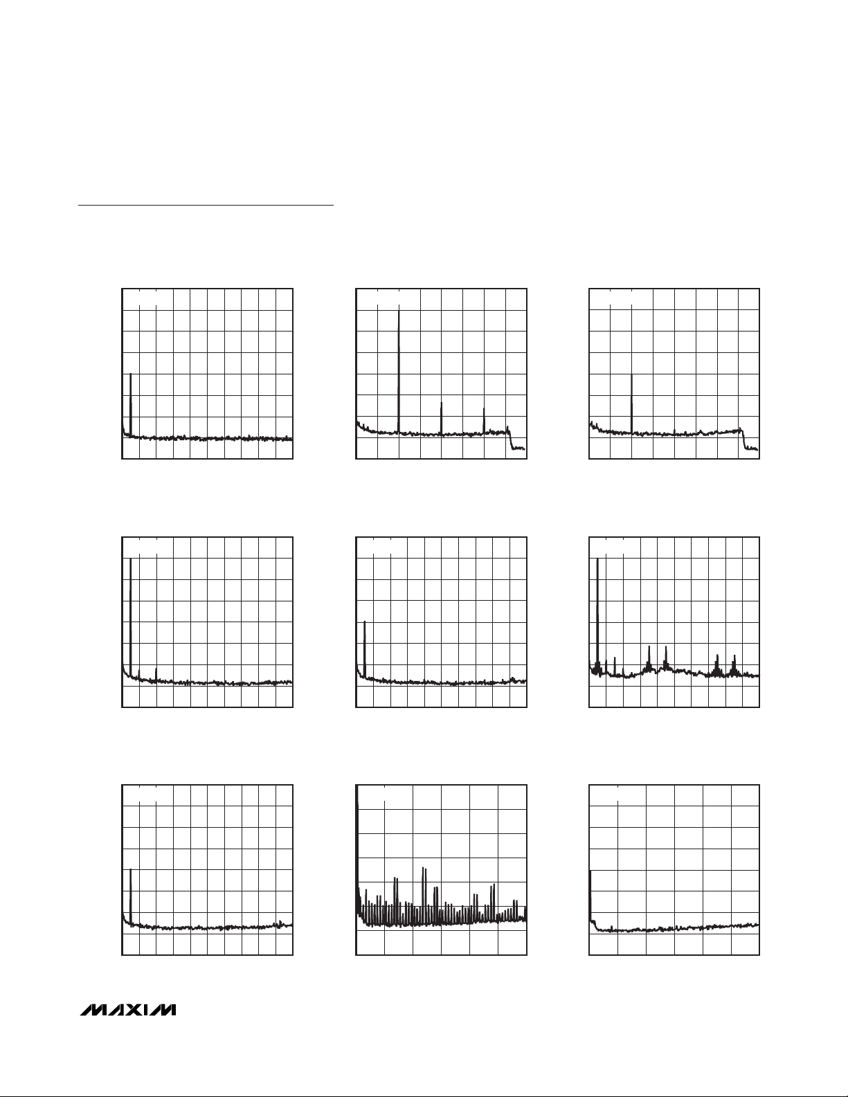
Typical Operating Characteristics
(V
AVDD
= V
DVDD
= V
PVDD
= +1.8V, C
REF
= 2.2µF, C
MICBIAS
= C
PREG
= C
REG
= 1µF, AV
MICPGA
= 0dB, MCLK = 13MHz, LRCLK =
8kHz, BW = 20Hz to fS/2, TA= +25°C, unless otherwise noted.)
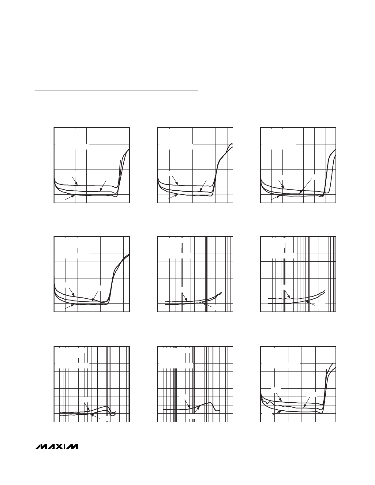
TOTAL HARMONIC DISTORTION + NOISE
vs. POWER OUT (DAC TO HEADPHONE)
0
MCLK = 13MHz
-10
LRCLK = 8kHz
= 32Ω
R
LOAD
-20
DIFFERENTIAL MODE
-30
-40
-50
THD+N (dB)
-60
-70
-80
-90
3kHz
20Hz
035
1510 3052520
POWER OUT (mW)
1kHz
MAX9867 toc01
TOTAL HARMONIC DISTORTION + NOISE
vs. POWER OUT (DAC TO HEADPHONE)
0
MCLK = 12.288MHz
-10
LRCLK = 48kHz
= 16Ω
-20
-30
-40
-50
THD+N (dB)
-60
-70
-80
-90
0
R
LOAD
DIFFERENTIAL MODE
6kHz
20Hz
POWER OUT (mW)
1kHz
50402010 30 60
MAX9867 toc04
TOTAL HARMONIC DISTORTION + NOISE
vs. POWER OUT (DAC TO HEADPHONE)
0
MCLK = 13MHz
-10
LRCLK = 8kHz
= 16Ω
R
LOAD
-20
DIFFERENTIAL MODE
-30
-40
-50
THD+N (dB)
-60
-70
-80
-90
3kHz
20Hz
0
TOTAL HARMONIC DISTORTION + NOISE
vs. FREQUENCY (DAC TO HEADPHONE)
0
MCLK = 13MHz
-10
LRCLK = 8kHz
= 32Ω
R
LOAD
-20
DIFFERENTIAL MODE
-30
-40
-50
THD+N (%)
-60
-70
-80
-90
10 10,000
POWER OUT (mW)
5mW
FREQUENCY (Hz)
1kHz
1000100
50402010 30 60
20mW
MAX9867 toc02
MAX9867 toc05
TOTAL HARMONIC DISTORTION + NOISE
vs. POWER OUT (DAC TO HEADPHONE)
0
MCLK = 12.288MHz
-10
LRCLK = 48kHz
= 32Ω
R
LOAD
-20
DIFFERENTIAL MODE
-30
-40
-50
THD+N (dB)
-60
-70
-80
-90
6kHz
20Hz
035
1510 3052520
POWER OUT (mW)
1kHz
TOTAL HARMONIC DISTORTION + NOISE
vs. FREQUENCY (DAC TO HEADPHONE)
0
MCLK = 13MHz
-10
LRCLK = 8kHz
= 16Ω
R
LOAD
-20
DIFFERENTIAL MODE
-30
-40
-50
THD+N (%)
-60
-70
-80
-90
10 10,000
5mW
20mW
1000100
FREQUENCY (Hz)
MAX9867 toc03
MAX9867 toc06
TOTAL HARMONIC DISTORTION + NOISE
vs. FREQUENCY (DAC TO HEADPHONE)
0
MCLK = 12.288MHz
-10
LRCLK = 48kHz
= 32Ω
R
LOAD
-20
DIFFERENTIAL MODE
-30
-40
-50
THD+N (%)
-60
-70
-80
-90
10 1000 100,000
5mW
20mW
100 10,000
FREQUENCY (Hz)
MAX9867 toc07
TOTAL HARMONIC DISTORTION + NOISE
vs. FREQUENCY (DAC TO HEADPHONE)
0
MCLK = 12.288MHz
-10
LRCLK = 48kHz
= 16Ω
R
LOAD
-20
DIFFERENTIAL MODE
-30
-40
-50
THD+N (%)
-60
-70
-80
-90
10 1000 100,000
5mW
20mW
100 10,000
FREQUENCY (Hz)
MAX9867 toc08
TOTAL HARMONIC DISTORTION + NOISE
vs. POWER OUT (DAC TO HEADPHONE)
0
MCLK = 13MHz
-10
LRCLK = 8kHz
= 32Ω
R
LOAD
-20
CAPACITORLESS MODE
-30
-40
-50
THD+N (dB)
-60
-70
-80
-90
3kHz
20Hz
0
410682
POWER OUT (mW)
MAX9867 toc09
1kHz
Page 14
MAX9867
Ultra-Low Power Stereo Audio Codec
14 ______________________________________________________________________________________
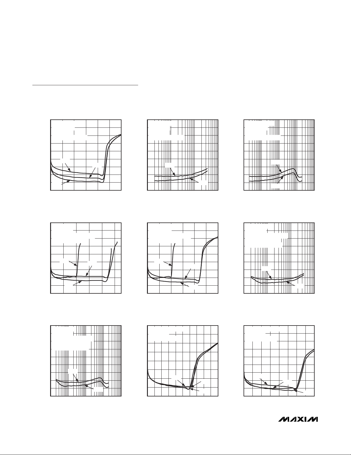
Typical Operating Characteristics (continued)
(V
AVDD
= V
DVDD
= V
PVDD
= +1.8V, C
REF
= 2.2μF, C
MICBIAS
= C
PREG
= C
REG
= 1μF, AV
MICPGA
= 0dB, MCLK = 13MHz, LRCLK =
8kHz, BW = 20Hz to f
S
/2, TA= +25°C, unless otherwise noted.)
TOTAL HARMONIC DISTORTION + NOISE
vs. POWER OUT (DAC TO HEADPHONE)
0
MCLK = 12.288MHz
-10
LRCLK = 48kHz
= 32
R
Ω
LOAD
-20
CAPACITORLESS MODE
-30
-40
-50
THD+N (dB)
-60
-70
-80
-90
6kHz
20Hz
0
POWER OUT (mW)
1kHz
81042126
MAX9867 toc10
TOTAL HARMONIC DISTORTION + NOISE
vs. FREQUENCY (DAC TO HEADPHONE)
0
MCLK = 13MHz
-10
LRCLK = 8kHz
= 32
R
Ω
LOAD
-20
CAPACITORLESS MODE
-30
-40
-50
THD+N (%)
-60
-70
-80
-90
10 10,000
1mW
1000100
FREQUENCY (Hz)
5mW
MAX9867 toc11
TOTAL HARMONIC DISTORTION + NOISE
vs. FREQUENCY (DAC TO HEADPHONE)
0
MCLK = 12.288MHz
-10
LRCLK = 48kHz
= 32
R
Ω
LOAD
-20
CAPACITORLESS MODE
-30
-40
-50
THD+N (%)
-60
-70
-80
-90
10 1000 100,000
1mW
5mW
100 10,000
FREQUENCY (Hz)
MAX9867 toc12
TOTAL HARMONIC DISTORTION + NOISE
vs. POWER OUT (DAC TO HEADPHONE)
0
MCLK = 13MHz
-10
LRCLK = 8kHz
-20
-30
-40
-50
THD+N (dB)
-60
-70
-80
-90
0
= 32Ω, C
R
LOAD
SINGLE-ENDED MODE
20Hz
OUT
1kHz
410682
POWER OUT (mW)
= 220μF
3kHz
TOTAL HARMONIC DISTORTION + NOISE
vs. FREQUENCY (DAC TO HEADPHONE)
0
MCLK = 13MHz
-10
LRCLK = 8kHz
= 32Ω, C
R
LOAD
-20
SINGLE-ENDED MODE
SPECIFIED AT 1kHz
P
OUT
-30
-40
-50
THD+N (%)
-60
-70
-80
-90
10 1000 100,000
= 220μF
OUT
1mW
5mW
100 10,000
FREQUENCY (Hz)
MAX9867 toc13
MAX9867 toc16
TOTAL HARMONIC DISTORTION + NOISE
vs. POWER OUT (DAC TO HEADPHONE)
0
MCLK = 12.288MHz
-10
LRCLK = 48kHz
-20
-30
-40
-50
THD+N (dB)
-60
-70
-80
-90
0
= 32Ω, C
R
LOAD
SINGLE-ENDED MODE
20Hz
= 220μF
OUT
6kHz
1kHz
POWER OUT (mW)
MAX9867 toc14
810426 12
TOTAL HARMONIC DISTORTION + NOISE
vs. POWER OUT (LINE IN TO HEADPHONE)
0
LINE IN PREAMP = +18dB
= 32
R
-10
-20
-30
-40
THD+N (dB)
-50
-60
-70
-80
050
Ω
LOAD
DIFFERENTIAL MODE
20Hz
POWER OUT (mW)
MAX9867 toc17
1kHz
6kHz
402515 2010 4535305
TOTAL HARMONIC DISTORTION + NOISE
vs. FREQUENCY (DAC TO HEADPHONE)
0
MCLK = 13MHz
-10
LRCLK = 8kHz
= 32Ω, C
R
LOAD
-20
SINGLE-ENDED MODE
SPECIFIED AT 1kHz
P
OUT
-30
-40
-50
THD+N (%)
-60
-70
-80
-90
10 10,000
TOTAL HARMONIC DISTORTION + NOISE
vs. POWER OUT (LINE IN TO HEADPHONE)
0
LINE IN PREAMP = 0dB
-10
-20
-30
-40
-50
THD+N (dB)
-60
-70
-80
-90
= 32
R
LOAD
DIFFERENTIAL MODE
6kHz
040
= 220μF
OUT
1mW
FREQUENCY (Hz)
Ω
POWER OUT (mW)
MAX9867 toc15
5mW
1000100
MAX9867 toc18
20Hz
1kHz
2510 20 3530155
Page 15
MAX9867
Ultra-Low Power Stereo Audio Codec
______________________________________________________________________________________ 15
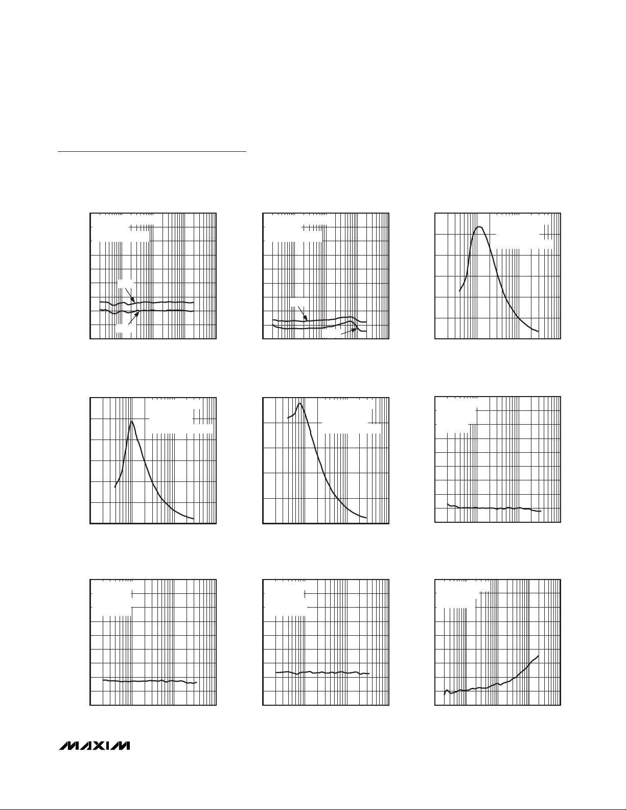
Typical Operating Characteristics (continued)
(V
AVDD
= V
DVDD
= V
PVDD
= +1.8V, C
REF
= 2.2μF, C
MICBIAS
= C
PREG
= C
REG
= 1μF, AV
MICPGA
= 0dB, MCLK = 13MHz, LRCLK =
8kHz, BW = 20Hz to f
S
/2, TA= +25°C, unless otherwise noted.)
TOTAL HARMONIC DISTORTION + NOISE
vs. FREQUENCY (LINE IN TO HEADPHONE)
0
LINE IN PREAMP = +18dB
-10
-20
-30
-40
-50
THD+N (dB)
-60
-70
-80
-90
= 32
R
Ω
LOAD
DIFFERENTIAL MODE
5mW
20mW
100 10,000
10 1000 100,000
POWER OUT vs. HEADPHONE LOAD
30
25
20
15
POWER OUT (mW)
10
5
0
1 100 1000
HEADPHONE LOAD (Ω)
FREQUENCY (Hz)
MCLK = 12.288MHz
LRCLK = 48kHz
THD+N = < 0.1%
CAPACITORLESS MODE
10
MAX9867 toc19
MAX9867 toc22
TOTAL HARMONIC DISTORTION + NOISE
vs. FREQUENCY (LINE IN TO HEADPHONE)
0
-10
-20
-30
-40
-50
THD+N (dB)
-60
-70
-80
-90
10 1000 100,000
25
20
15
10
POWER OUT (mW)
5
0
1 100 1000
LINE IN PREAMP = +18dB
= 32
R
Ω
LOAD
DIFFERENTIAL MODE
5mW
100 10,000
20mW
FREQUENCY (Hz)
POWER OUT vs. HEADPHONE LOAD
MCLK = 12.288MHz
LRCLK = 48kHz
THD+N = < 0.1%
SINGLE-ENDED MODE
10
HEADPHONE LOAD (Ω)
MAX9867 toc20
MAX9867 toc23
POWER OUT vs. HEADPHONE LOAD
60
50
40
30
POWER OUT (mW)
20
10
0
1 100 1000
MCLK = 12.288MHz
LRCLK = 48kHz
THD+N = < 0.1%
DIFFERENTIAL MODE
10
HEADPHONE LOAD (Ω)
TOTAL HARMONIC DISTORTION + NOISE
vs. FREQUENCY (MICROPHONE TO ADC)
0
MCLK = 13MHz
-10
LRCLK = 8kHz
MICPRE = 0dB
-20
= 1V
V
IN
-30
-40
-50
THD+N (%)
-60
-70
-80
-90
P-P
10 10,000
FREQUENCY (Hz)
1000100
MAX9867 toc21
MAX9867 toc24
TOTAL HARMONIC DISTORTION + NOISE
vs. FREQUENCY (MICROPHONE TO ADC)
0
MCLK = 13MHz
-10
LRCLK = 8kHz
MICPRE = 20dB
-20
= 0.11V
V
IN
-30
-40
-50
THD+N (%)
-60
-70
-80
-90
10 10,000
P-P
1000100
FREQUENCY (Hz)
MAX9867 toc25
TOTAL HARMONIC DISTORTION + NOISE
vs. FREQUENCY (MICROPHONE TO ADC)
0
MCLK = 13MHz
-10
LRCLK = 8kHz
MICPRE = 30dB
-20
= 0.032V
V
IN
-30
-40
-50
THD+N (%)
-60
-70
-80
-90
10 10,000
P-P
1000100
FREQUENCY (Hz)
MAX9867 toc26
POWER-SUPPLY REJECTION RATIO
vs. FREQUENCY (DAC TO HEADPHONE)
0
V
= 100mV
RIPPLE
-10
MCLK = 13MHz
LRCLK = 8kHz
-20
-30
-40
-50
PSRR (dB)
-60
-70
-80
-90
10 1000 100,000
P-P
100 10,000
FREQUENCY (Hz)
MAX9867 toc27
Page 16
MAX9867
Ultra-Low Power Stereo Audio Codec
16 ______________________________________________________________________________________
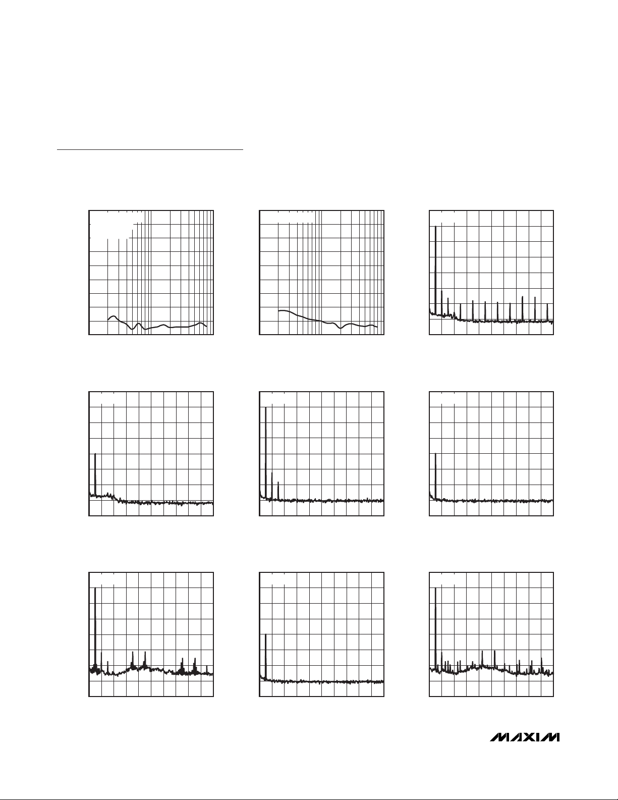
Typical Operating Characteristics (continued)
(V
AVDD
= V
DVDD
= V
PVDD
= +1.8V, C
REF
= 2.2μF, C
MICBIAS
= C
PREG
= C
REG
= 1μF, AV
MICPGA
= 0dB, MCLK = 13MHz, LRCLK =
8kHz, BW = 20Hz to f
S
/2, TA= +25°C, unless otherwise noted.)
POWER-SUPPLY REJECTION RATIO
vs. FREQUENCY (MIC TO ADC)
0
V
= 100mV
RIPPLE
-10
MCLK = 13MHz
LRCLK = 8kHz
-20
-30
-40
-50
PSRR (dB)
-60
-70
-80
-90
10 100 1000
P-P
FREQUENCY (Hz)
MAX9867 toc28
POWER-SUPPLY REJECTION RATIO
vs. FREQUENCY (MICBIAS)
0
V
= 100mV
RIPPLE
-10
-20
-30
-40
-50
PSRR (dB)
-60
-70
-80
-90
10 100 1000
P-P
FREQUENCY (Hz)
MAX9867 toc29
FFT, DAC TO HEADPHONE,
0dBFS, MCLK = 13MHz, LRCLK = 8kHz
20
FREQ = 0xA
0
-20
-40
-60
-80
AMPLITUDE (dB)
-100
-120
-140
061218
FREQUENCY (kHz)
MAX9867 toc30
20281016414
FFT, DAC TO HEADPHONE,
-60dBFS, MCLK = 13MHz, LRCLK = 8kHz
20
FREQ = 0xA
0
-20
-40
-60
-80
AMPLITUDE (dB)
-100
-120
-140
0 6 12 18
FREQUENCY (kHz)
FFT, DAC TO HEADPHONE,
0dBFS, MCLK = 13MHz, LRCLK = 48kHz
20
PLL MODE
0
-20
-40
-60
-80
AMPLITUDE (dB)
-100
-120
-140
0 6 12 18
FREQUENCY (kHz)
MAX9867 toc31
202 8 10 16414
MAX9867 toc34
202 8 10 16414
FFT, DAC TO HEADPHONE,
0dBFS, MCLK = 12.288MHz, LRCLK = 48kHz
20
NI = 6000
0
-20
-40
-60
-80
AMPLITUDE (dB)
-100
-120
-140
0 6 12 18
FREQUENCY (kHz)
FFT, DAC TO HEADPHONE,
-60dBFS, MCLK = 13MHz, LRCLK = 48kHz
20
PLL MODE
0
-20
-40
-60
-80
AMPLITUDE (dB)
-100
-120
-140
0 6 12 18
FREQUENCY (kHz)
MAX9867 toc32
202 8 10 16414
MAX9867 toc35
202 8 10 16414
-60dBFS, MCLK = 12.288MHz, LRCLK = 48kHz
FFT, DAC TO HEADPHONE,
20
NI = 6000
0
-20
-40
-60
-80
AMPLITUDE (dB)
-100
-120
-140
061218
FREQUENCY (kHz)
FFT, DAC TO HEADPHONE,
0dBFS, MCLK = 13MHz, LRCLK = 44.1kHz
20
PLL MODE
0
-20
-40
-60
-80
AMPLITUDE (dB)
-100
-120
-140
061218
FREQUENCY (kHz)
MAX9867 toc33
20281016414
MAX9867 toc36
20281016414
Page 17
MAX9867
Ultra-Low Power Stereo Audio Codec
______________________________________________________________________________________ 17
Typical Operating Characteristics (continued)
(V
AVDD
= V
DVDD
= V
PVDD
= +1.8V, C
REF
= 2.2μF, C
MICBIAS
= C
PREG
= C
REG
= 1μF, AV
MICPGA
= 0dB, MCLK = 13MHz, LRCLK =
8kHz, BW = 20Hz to f
S
/2, TA= +25°C, unless otherwise noted.)
FFT, DAC TO HEADPHONE, -60dBFS,
MCLK = 13MHz, LRCLK = 44.1kHz
20
PLL MODE
0
-20
-40
-60
-80
AMPLITUDE (dB)
-100
-120
-140
0 6 12 18
FREQUENCY (kHz)
FFT, MICROPHONE TO ADC,
0dBFS, MCLK = 12.288MHz, LRCLK = 48kHz
20
NI = 6000
0
-20
-40
-60
-80
AMPLITUDE (dB)
-100
-120
-140
0 6 12 18
FREQUENCY (kHz)
202 8 10 16414
202 8 10 16414
FFT, MICROPHONE TO ADC,
0dBFS, MCLK = 13MHz, LRCLK = 8kHz
20
FREQ = 0xA
MAX9867 toc37
0
-20
-40
-60
-80
AMPLITUDE (dB)
-100
-120
-140
1000 3000
0 2000 4000500 25001500 3500
FFT, MICROPHONE TO ADC,
-60dBFS, MCLK = 12.288MHz, LRCLK = 48kHz
20
NI = 6000
MAX9867 toc40
0
-20
-40
-60
-80
AMPLITUDE (dB)
-100
-120
-140
0 6 12 18
FREQUENCY (Hz)
FREQUENCY (kHz)
202 8 10 16414
MAX9867 toc38
MAX9867 toc41
FFT, MICROPHONE TO ADC,
-60dBFS, MCLK = 13MHz, LRCLK = 8kHz
20
FREQ = 0xA
0
-20
-40
-60
-80
AMPLITUDE (dB)
-100
-120
-140
1000 3000
0 2000 4000500 25001500 3500
FREQUENCY (Hz)
FFT, MICROPHONE TO ADC,
0dBFS, MCLK = 13MHz, LRCLK = 48kHz
20
PLL MODE
0
-20
-40
-60
-80
AMPLITUDE (dB)
-100
-120
-140
061218
FREQUENCY (kHz)
MAX9867 toc39
MAX9867 toc42
20281016414
FFT, MICROPHONE TO ADC,
-60dBFS, MCLK = 13MHz, LRCLK = 48kHz
20
PLL MODE
0
-20
-40
-60
-80
AMPLITUDE (dB)
-100
-120
-140
0 6 12 18
FREQUENCY (kHz)
MAX9867 toc43
202 8 10 16414
WIDEBAND FFT, DAC TO HEADPHONE,
0dBFS, MCLK = 13MHz, LRCLK = 8kHz
0
FREQ = 0xA
-20
-40
-60
-80
AMPLITUDE (dB)
-100
-120
-140
0 60 12020 80
40 100
FREQUENCY (kHz)
MAX9867 toc44
WIDEBAND FFT, DAC TO HEADPHONE,
-60dBFS, MCLK = 13MHz, LRCLK = 8kHz
20
FREQ = 0xA
0
-20
-40
-60
-80
AMPLITUDE (dB)
-100
-120
-140
06012020 80
40 100
FREQUENCY (kHz)
MAX9867 toc45
Page 18

MAX9867
Ultra-Low Power Stereo Audio Codec
18 ______________________________________________________________________________________
Typical Operating Characteristics (continued)
(V
AVDD
= V
DVDD
= V
PVDD
= +1.8V, C
REF
= 2.2μF, C
MICBIAS
= C
PREG
= C
REG
= 1μF, AV
MICPGA
= 0dB, MCLK = 13MHz, LRCLK =
8kHz, BW = 20Hz to f
S
/2, TA= +25°C, unless otherwise noted.)
20
0
-20
-40
AMPLITUDE (dB)
-60
-80
-100
20
DAC IIR HIGHPASS FILTER
FREQUENCY RESPONSE, MODE = 0
DVFLT = 0
DVFLT = 3
DVFLT = 4
220 520320 420120
FREQUENCY (Hz)
LRCLK = 8kHz
MODE = 0
MAX9867 toc46
DAC IIR HIGHPASS FILTER
FREQUENCY RESPONSE, MODE = 0
20
AVFLT = 0
0
AVFLT = 3
-20
-40
AMPLITUDE (dB)
-60
-80
-100
20
AVFLT = 4
220 520320 420120
FREQUENCY (Hz)
LRCLK = 8kHz
MAX9867 toc47
DAC IIR/FIR LOWPASS FILTER
FREQUENCY RESPONSE (8kHz)
20
10
0
-10
-20
-30
-40
AMPLITUDE (dB)
-50
-60
-70
-80
3.0 3.3 3.6 3.9
MODE = 0
FREQUENCY (kHz)
MODE = 1
MAX9867 toc48
4.03.1 3.4 3.5 3.83.2 3.7
ADC IIR/FIR LOWPASS FILTER
FREQUENCY RESPONSE (8kHz)
20
10
-20
-40
AMPLITUDE (dB)
-60
-80
-100
3.0 3.3 3.6 3.9
MODE = 1
MODE = 0
FREQUENCY (kHz)
SHUTDOWN TO DAC FULL OPERATION
(CLICKLESS SINGLE-ENDED MODE)
4.03.1 3.4 3.5 3.83.2 3.7
MAX9867 toc49
MAX9867 toc51
SHUTDOWN TO DAC FULL OPERATION
(CAPACITORLESS OR DIFFERENTIAL MODE)
MAX9867 toc50
LOUTP (500mV/div) SCL (2V/div)
TIME (4ms/div)
SHUTDOWN TO DAC FULL OPERATION
(FAST TURN-ON SINGLE-ENDED MODE)
MAX9867 toc52
LOUTP (500mV/div) SCL (2V/div)
TIME (40ms/div)
LOUTP (500mV/div) SCL (2V/div)
TIME (4ms/div)
Page 19

MAX9867
Ultra-Low Power Stereo Audio Codec
______________________________________________________________________________________ 19
Typical Operating Characteristics (continued)
(V
AVDD
= V
DVDD
= V
PVDD
= +1.8V, C
REF
= 2.2μF, C
MICBIAS
= C
PREG
= C
REG
= 1μF, AV
MICPGA
= 0dB, MCLK = 13MHz, LRCLK =
8kHz, BW = 20Hz to f
S
/2, TA= +25°C, unless otherwise noted.)
FULL OPERATION TO SHUTDOWN (DAC)
LOUTP (500mV/div) SCL (2V/div)
TOTAL HARMONIC DISTORTION + NOISE
vs. MCLK FREQUENCY, 0dBFS
0
LRCLK = 48kHz
-10
PLL MODE
-20
-30
-40
-50
THD+N (dB)
-60
-70
-80
-90
-100
2015 40 5025 5545
10 6030 35
MCLK FREQUENCY (MHz)
TIME (1ms/div)
MAX9867 toc53
MAX9867 toc55
ADC SOFT-START
ADC OUT (500mV/div) SCL (2V/div)
TIME (4ms/div)
DYNAMIC RANGE vs. MCLK FREQUENCY
120
VIN = -60dBFS
LRCLK = 48kHz
110
PLL MODE
A-WEIGHTED
100
90
80
DYNAMIC RANGE (dB)
70
60
10 100
MCLK FREQUENCY (MHz)
MAX9867 toc54
MAX9867 toc56
LINE INPUT RESISTANCE vs. GAIN SETTING
270
220
170
120
INPUT RESISTANCE (kΩ)
70
20
-6 4 14 24-1 9 19
GAIN SETTING (dB)
MAX9867 toc57
30,000
25,000
20,000
15,000
10,000
5000
AUX CODE (SIGNED DECIMAL)
-5000
AUX CODE vs. INPUT VOLTAGE
MAX9867 toc58
0
-0.4 0.80.2 1.20.60.401.0-0.2
INPUT VOLTAGE (V)
Page 20

MAX9867
Ultra-Low Power Stereo Audio Codec
20 ______________________________________________________________________________________
Pin Description
PIN/BUMP
TQFN-EP WLP
1 A2 DGND Digital Ground
2 B3 SCL I2C Serial-Clock Input. Connect a pullup resistor to a 1.7V to 3.3V supply.
3 A3 SDA I2C Serial-Data Input/Output. Connect a pullup resistor to a 1.7V to 3.3V supply.
4C3 IRQ
5 A4 AVDD Analog Power Supply. Bypass to AGND with a 1μF capacitor.
6 B4 REF Converter Reference. Bypass to AGND with a 2.2μF capacitor (1.23V nominal).
7 A5 PREG
8 B5 REG PREG/2 Voltage Reference. Bypass to AGND with a 1μF capacitor (0.8V nominal).
9 A6 AGND Analog Ground
10 B6 MICBIAS
11 C5
12 C6
13 C4 MICRP
14 D6 MICRN
15 D5 LINL Left-Line Input. AC-couple analog audio signal to LINL with a 1μF capacitor.
16 E6 LINR Right-Line Input. AC-couple analog audio signal to LINR with a 1μF capacitor.
17 D4 JACKSNS/AUX
18 E5 PGND Headphone Power Ground
19 D3 ROUTP
20 E4 ROUTN
21 D2 LOUTN
NAME FUNCTION
Hardware Interrupt Output. IRQ can be programmed to pull low when bits in
status register 0x00 are set. Read status register 0x00 to clear IRQ once set.
Repeat faults have no effect on IRQ until it is cleared by reading register 0x00.
Connect a 10kΩ pullup resistor to a 1.7V to 3.3V supply.
Positive Internal Regulated Supply. Bypass to AGND with a 1μF capacitor (1.6V
nominal).
Low-Noise Microphone Bias. Connect a 2.2kΩ to 470Ω resistor to the positive
output of a microphone (1.525V nominal). Bypass to AGND with a 1μF capacitor.
Left Negative Differential Microphone Input or Digital Microphone Clock Output.
MICLN/
DIGMICCLK
MICLP/
DIGMICDATA
For analog microphones, AC-couple to the negative output of a microphone with a
1μF capacitor. For digital microphones, connect to the clock input of the
microphone.
Left Positive Differential Microphone Input or Digital Microphone Data Input. For
analog microphones, AC-couple to the positive output of a microphone with a 1μF
capacitor. For digital microphones, connect to the data output of the
microphone(s). Up to two digital microphones can be connected.
Right Positive Differential Microphone Input. AC-couple to the positive output of a
microphone with a 1μF capacitor.
Right Negative Differential Microphone Input. AC-couple to the negative output of
a microphone with a 1μF capacitor.
Jack Sense or Auxiliary ADC Input. When configured for jack detection, JACKSNS
detects the presence or absence of a jack. See the Mode Configuration section
for details. When configured as an auxiliary ADC input, AUX is used to measure
DC voltages.
Positive Right-Channel Headphone Output. Connect directly to the load in
differential and capacitorless mode. AC-couple to the load in single-ended mode.
Negative Right-Channel Headphone Output. Inverting output in differential mode.
Leave unconnected in capacitorless and fast turn-on single-ended mode. Bypass
with a 1μF capacitor to AGND in clickless, single-ended mode.
Negative Left-Channel Headphone Output. Noninverting output in differential
mode. Common headphone return in capacitorless mode. Leave unconnected in
fast turn-on single-ended mode. Bypass with a 1μF capacitor to AGND in clickless
single-ended mode.
Page 21

Detailed Description
The MAX9867 is a low-power stereo audio codec
designed for portable applications requiring minimum
power consumption.
The stereo playback path accepts digital audio through
a flexible interface compatible with I2S, TDM, and leftjustified signals. An oversampling sigma-delta DAC
converts the incoming digital data stream to analog
audio and outputs the audio through the stereo headphone amplifier. The headphone amplifier can be configured in differential, single-ended, and capacitorless
output modes.
The stereo record path has two analog microphone
inputs with selectable gain. An integrated microphone
bias can be used to power the microphones. The left
analog microphone inputs can also accept data from
up to two digital microphones. An oversampling sigmadelta ADC converts the microphone signals and outputs the digital bit stream over the digital audio
interface.
Integrated digital filtering provides a range of notch and
highpass filters for both the playback and record paths
to limit undesirable low-frequency signals and GSM
transmission noise. The digital filtering provides attenuation
of out-of-band energy by over 70dB, eliminating audible aliasing. A digital sidetone function allows audio
from the record path to be summed into the playback
path after digital filtering.
The MAX9867 also includes two stereo, single-ended
line inputs with gain adjustment, which can be recorded by the ADCs and/or output by the headphone amplifiers. An auxiliary ADC accurately measures a DC
voltage by utilizing the right audio ADC and reporting
the DC voltage through the I
2
C interface. A jack detection function allows the detection of headphone, microphone, and headset jacks. Insertion and removal
events can be programmed to trigger a hardware interrupt and flag an I2C register bit.
The MAX9867’s flexible clock circuitry utilizes a programmable clock divider and a digital PLL, allowing the DAC
and ADC to operate at maximum dynamic range for all
combinations of master clock (MCLK) and sample rate
(LRCLK) without consuming extra supply current. Any
master clock between 10MHz and 60MHz is supported
as are all sample rates from 8kHz to 48kHz. Master and
slave modes are supported for maximum flexibility.
MAX9867
Ultra-Low Power Stereo Audio Codec
______________________________________________________________________________________ 21
Pin Description (continued)
PIN/BUMP
TQFN-EP WLP
22 E3 LOUTP
23 E2 PVDD Headphone Power Supply. Bypass to PGND with a 1μF capacitor.
24, 25 — N.C. No Connection
26 E1 DVDDIO Digital Audio Interface Power Supply. Bypass to DGND with a 1μF capacitor.
27 D1 SDOUT Digital Audio Serial-Data ADC Output
28 C2 SDIN Digital Audio Serial-Data DAC Input
29 C1 LRCLK
30 B1 BCLK
31 B2 MCLK Master Clock Input. Acceptable input frequency range: 10MHz to 60MHz.
32 A1 DVDD
— — EP Exposed Pad. Connect the exposed thermal pad to AGND.
NAME FUNCTION
Positive Left-Channel Headphone Output. Connect directly to the load in
differential and capacitorless mode. AC-couple to the load in single-ended mode.
Digital Audio Left-Right Clock Input/Output. LRCLK is the audio sample rate clock
and determines whether the audio data on SDIN is routed to the left or right
channel. In TDM mode, LRCLK is a frame synchronization pulse. LRCLK is an
input when the MAX9867 is in slave mode and an output when in master mode.
Digital Audio Bit Clock Input/Output. BCLK is an input when the MAX9867 is in
slave mode and an output when in master mode.
Digital Power Supply. Supply for the digital circuitry and I
DGND with a 1μF capacitor.
2
C interface. Bypass to
Page 22

MAX9867
I2C Registers
The MAX9867 audio codec is completely controlled
through software using an I2C interface. The power-on
default setting is complete shutdown, requiring that the
internal registers be programmed to activate the device.
See Table 1 for the device’s complete register map.
I2C Slave Address
The MAX9867 responds to the slave address 0x30 for
all write commands and 0x31 for all read operations.
Ultra-Low Power Stereo Audio Codec
22 ______________________________________________________________________________________
Table 1. I2C Register Map
REGISTER B7 B6 B5 B4 B3 B2 B1 B0
STATUS
Status (Read Only) CLD SLD ULK 0 0 0 JDET 0 0x00 —
Jack Sense (Read Only) LSNS JKSNS JKMIC 0 0 0 0 0 0x01 —
AUX High (Read Only) AUX[15:8] 0x02 —
AUX Low (Read Only) AUX[7:0] 0x03 —
Interrupt Enable ICLD ISLD IULK 0 0 SDODLY IJDET 0 0x04 0x00
CLOCK CONTROL
System Clock 0 0 PSCLK FREQ 0x05 0x00
Stereo Audio Clock
Control High
Stereo Audio Clock
Control Low
DIGITAL AUDIO INTERFACE
Interface Mode MAS WCI BCI DLY HIZOFF TDM 0 0 0x08 0x00
Interface Mode 0 0 0 LVOLFIX DMONO BSEL 0x09 0x00
DIGITAL FILTERING
Codec Filters MODE AVFLT 0 DVFLT 0x0A 0x00
LEVEL CONTROL
Sidetone DSTS 0 DVST 0x0B 0x00
DAC Level 0 DACM DACG DACA 0x0C 0x00
ADC Level AVL AVR 0x0D 0x00
Left-Line Input Level 0 LILM 0 0 LIGL 0x0E 0x00
Right-Line Input Level 0 LIRM 0 0 LIGR 0x0F 0x00
Left Volume Control 0 VOLLM VOLL 0x10 0x00
Right Volume Control 0 VOLRM VOLR 0x11 0x00
Left Microphone Gain 0 PALEN PGAML 0x12 0x00
Right Microphone Gain 0 PAREN PGAMR 0x13 0x00
CONFIGURATION
ADC Input MXINL MXINR AUXCAP AUXGAIN AUXCAL AUXEN 0x14 0x00
Microphone MICCLK DIGMICL DIGMICR 0 0 0 0 0x15 0x00
Mode DSLEW VSEN ZDEN 0 JDETEN HPMODE 0x16 0x00
POWER MANAGEMENT
System Shutdown SHDN LNLEN LNREN 0 DALEN DAREN ADLEN ADREN 0x17 0x00
Revision REV 0xFF 0x42
PLL NI[14:8] 0x06 0x00
NI[7:1]
RLK/
NI[0]
REGISTER
ADDRESS
0x07 0x00
POWER-
ON RESET
STATE
Page 23

Device Status
Status registers 0x00 and 0x01 are read-only registers
that report the status of various device functions. The
status register bits are cleared upon reading the status
register and are set the next time the event occurs.
Registers 0x02 and 0x03 report the DC level applied to
AUX. See the
ADC
section for more details and Table 2.
MAX9867
Ultra-Low Power Stereo Audio Codec
______________________________________________________________________________________ 23
Table 2. Status Registers
REGISTER B7 B6 B5 B4 B3 B2 B1 B0
Status (Read Only) CLD SLD ULK 0 0 0 JDET 0 0x00
Jack S ense ( Read O nl y) LSNS JKSNS JKMIC 0 0 0 0 0 0x01
AUX High (Read Only) AUX[15:8] 0x02
AUX Low (Read Only) AUX[7:0] 0x03
BITS FUNCTION
CLD
SLD
ULK
JDET
LSNS
JKSNS
JKMIC
AUX
Clip Detect Flag
Indicates that a signal has reached or exceeded full scale in the ADC or DAC.
Slew Level Detect Flag
When volume or gain changes are made, the slewing circuitry smoothly steps through all intermediate
settings. When SLD is set high, all slewing has completed and the volume or gain is at its final value. SLD
is also set when soft-start or stop is complete.
Digital PLL Unlock Flag
Indicates that the digital audio PLL has become unlocked and digital signal data is not reliable.
Headset Configuration Change Flag
JDET is set whenever there is a change in register 0x01, indicating that the headset configuration has
changed.
LOUTP State (Valid if SHDN = 0, JDETEN = 1)
LSNS is set when the voltage at LOUTP exceeds AVDD - 0.4V. An internal pullup from AVDD to LOUTP
causes this condition whenever there is no load on LOUTP. LSNS is only valid in differential and
capacitorless output modes.
JACKSNS State (Valid if JDETEN = 1)
JKSNS is set when the voltage at JACKSNS exceeds AVDD - 0.4V. An internal pullup from AVDD to
JACKSNS causes this condition whenever there is no load on JACKSNS.
Microphone Detection (Valid if PALEN or PAREN ≠ 00 and JDETEN = 1)
JKMIC is set when JACKSNS exceeds 0.95 x V
Auxiliary Input Measurement
AUX is a 16-bit signed two’s complement number representing the voltage measured at JACKSNS/AUX.
Before reading a value from AUX, set AUXCAP to 1 to ensure a stable reading. After reading the value,
set AUXCAP to 0.
Use the following formula to convert the AUX value into an equivalent JACKSNS/AUX voltage:
AUX
⎛
Voltage V
K = AUX value when AUXGAIN = 1. See the ADC section for complete details.
=×
0 738.
⎞
⎜
⎟
⎝
⎠
K
MICBIAS
.
REGISTER
ADDRESS
Page 24

MAX9867
Hardware Interrupts
Hardware interrupts are reported on the open-drain IRQ
pin. When an interrupt occurs, IRQ remains low until the
interrupt is serviced by reading the status register 0x00.
If a flag is set, it is reported as a hardware interrupt only
if the corresponding interrupt enable is set. Each bit
enables interrupts for the status flag in the respective
bit location in register 0x00. See Table 3.
SDODLY is used to control the SDOUT timing. See the
Digital Audio Interface
section for a detailed description.
Clock Control
The MAX9867 can work with a master clock (MCLK)
supplied from any system clock within the 10MHz-to60MHz range. Internally, the MAX9867 requires a
10MHz-to-20MHz clock. A prescaler divides MCLK by
1, 2, or 4 to create the internal clock (PCLK). PCLK is
used to clock all portions of the MAX9867. See Table 4.
The MAX9867 is capable of supporting any sample rate
from 8kHz to 48kHz, including all common sample rates
(8kHz, 16kHz, 24kHz, 32kHz, 44.1kHz, and 48kHz). To
accommodate a wide range of system architectures,
the MAX9867 supports three main clocking modes:
• Normal: This mode uses a 15-bit clock divider coeffi-
cient to set the sample rate relative to the prescaled
MCLK input (PCLK). This allows high flexibility in both
the MCLK and LRCLK frequencies and can be used
in either master or slave mode.
• Exact Integer: In both master and slave mode, com-
mon MCLK frequencies (12MHz, 13MHz, 16MHz,
and 19.2MHz) can be programmed to operate in
exact integer mode for both 8kHz and 16kHz sample
rates. In these modes, the MCLK and LRCLK rates
are selected by using the FREQ bits instead of the NI
and PLL control bits.
• PLL: When operating in slave mode, a PLL can be
enabled to lock onto externally generated LRCLK
signals that are not integer related to PCLK. Prior to
enabling the interface, program NI to the nearest
desired ratio and set the NI[0] = 1 to enable the
PLL’s rapid lock mode. If NI[0] = 0, then NI is ignored
and PLL lock time is slower.
Ultra-Low Power Stereo Audio Codec
24 ______________________________________________________________________________________
Table 3. Interrupt Registers
Table 4. Clock Control Registers
REGISTER B7 B6 B5 B4 B3 B2 B1 B0
Interrupt Enable ICLD ISLD IULK 0 0 SDODLY IJDET 0 0x04
REGISTER
ADDRESS
REGISTER B7 B6 B5 B4 B3 B2 B1 B0
System Clock 0 0 PSCLK FREQ 0x05
Stereo Audio Clock
Control High
Stereo Audio Clock
Control Low
BITS FUNCTION
MCLK Prescaler
Divides MCLK to generate a PCLK between 10MHz and 20MHz.
PSCLK
00 = Disable clock for low-power shutdown.
01 = Select if MCLK is between 10MHz and 20MHz.
10 = Select if MCLK is between 20MHz and 40MHz.
11 = Select if MCLK is between 40MHz and 60MHz.
PLL NI[14:8] 0x06
NI[7:1] NI[0] 0x07
REGISTER
Page 25

MAX9867
Ultra-Low Power Stereo Audio Codec
______________________________________________________________________________________ 25
Table 4. Clock Control Registers (continued)
Note: Bolded values are exact integers that provide maximum full-scale performance.
Table 5. Common NI Values
BITS FUNCTION
Exact Integer Modes
Allows integer sampling for specific PCLK (prescaled MCLK) frequencies and 8kHz or 16kHz sample rates.
FREQ[3:0] PCLK (MHz) LRCLK (kHz) PCLK/LRCLK
0x00 Normal or PLL mode
0x1–0x7 Reserved Reserved Reserved
FREQ
PLL
0x8
0x9
0xA
0xB
0xC
0xD
0xE
0xF
Modes 0x8–0xF are available in either master or slave mode. In slave mode, if the indicated PCLK/LRCLK ratio
cannot be guaranteed, use PLL mode instead.
PLL Mode Enable
0 = Valid for slave and master mode. The frequency of LRCLK is set by the NI divider bits. In master mode, the
MAX9867 generates LRCLK using the specified divide ratio. In slave mode, the MAX9867 expects an
LRCLK as specified by the divide ratio.
1 = Valid for slave mode only. A digital PLL locks on to any externally supplied LRCLK signal.
Rapid Lock Mode
To enable rapid lock mode, set NI to the nearest desired ratio and set NI[0] = 1 before enabling the interface.
Normal Mode LRCLK Divider
When PLL = 0, the frequency of LRCLK is determined by NI. See Table 5 for common NI values.
12
12
13
13
16
16
19.2
19.2
16
16
16
16
8
8
8
8
1500
750
1625
812.5
2000
1000
2400
1200
LRCLK
)/f
PCLK
NI
NI = (65536 x 96 x f
f
= LRCLK frequency
LRCLK
f
= Prescaled MCLK internal clock frequency (PCLK)
PCLK
LRCLK > 24kHz is only valid for MODE = 0 (stereo audio mode). MODE = 1 (voice mode) requires LRCLK ≤
24kHz.
MCLK (MHz)
11.2896 01 0x116A 0x22D4 0x343F 0x45A9 0x6000 0x687D
12 01 0x1062 0x20C5 0x3127 0x4189 0x5A51 0x624E
12.288 01 0x1000 0x2000 0x3000 0x4000 0x5833 0x6000
13 01 0x0F20 0x1E3F 0x2D5F 0x3C7F 0x535F 0x5ABE
19.2 01 0x0A3D 0x147B 0x1EB8 0x28F6 0x3873 0x3D71
24 10 0x1062 0x20C5 0x1893 0x4189 0x5A51 0x624E
26 10 0x0F20 0x1E3F 0x16AF 0x3C7F 0x535F 0x5ABE
27 10 0x0E90 0x1D21 0x15D8 0x3A41 0x5048 0x5762
PSCLK 8 16 24 32 44.1 48
LRCLK (kHz)
Page 26

MAX9867
Ultra-Low Power Stereo Audio Codec
26 ______________________________________________________________________________________
Table 6. Digital Audio Interface Registers
Digital Audio Interface
The MAX9867’s digital audio interface supports a wide
range of operating modes to ensure maximum compatibility. See Figures 1–4 for timing diagrams. In master
mode, the MAX9867 outputs LRCLK and BCLK, while in
slave mode they are inputs. When operating in master
mode, BCLK can be configured in a number of ways to
ensure compatiblity with other audio devices.
LVOLFIX is used to fix the line input playback volume to
0dB regardless of VOLL and VOLR. See the
Line Inputs
section for complete details and Table 6.
REGISTER B7 B6 B5 B4 B3 B2 B1 B0
Interface Mode MAS WCI BCI DLY HIZOFF TDM 0 0 0x08
Interface Mode 0 0 0 LVOLFIX DMONO BSEL 0x09
BITS FUNCTION
Master Mode
MAS
WCI
BCI
SDODLY
DLY
HIZOFF
LVOLFIX See the Line Inputs section.
0 = The MAX9867 operates in slave mode with LRCLK and BCLK configured as inputs.
1 = The MAX9867 operates in master mode with LRCLK and BCLK configured as outputs.
LRCLK Invert
0 = Left-channel data is input and output while LRCLK is low.
1 = Right-channel data is input and output while LRCLK is low.
Note: WCI is ignored when TDM = 1.
BCLK Invert
In master and slave modes:
0 = SDIN is latched into the part on the rising edge of BCLK.
SDOUT transitions after the rising edge of BCLK as determined by SDODLY.
1 = SDIN is latched into the part on the falling edge of BCLK.
SDOUT transitions after the falling edge of BCLK as determined by SDODLY.
In master mode:
0 = LRCLK changes state immediately after the rising edge of BCLK.
1 = LRCLK changes state immediately after the falling edge of BCLK.
SDOUT Delay
0 = SDOUT transitions one half BCLK cycle after SDIN is latched into the part.
1 = SDOUT transitions on the same BCLK edge as SDIN is latched into the part.
See Figures 1–4 for complete details. See Register 0x04 (interrupt registers).
Delay Mode
0 = SDIN/SDOUT data is latched on the first BCLK edge following an LRCLK edge.
1 = SDIN/SDOUT data is assumed to be delayed one BCLK cycle so that it is latched on the 2nd BCLK edge
following an LRCLK edge (I
Note: DLY is ignored when TDM = 1.
SDOUT High-Impedance Mode
0 = SDOUT goes to a high-impedance state after all data bits have been transferred out of the MAX9867,
allowing SDOUT to be shared by other devices.
1 = SDOUT is set either high or low after all data bits have been transferred out of the MAX9867.
Note: High-impedance mode is intended for use when TDM = 1.
2
S-compatible mode).
REGISTER
ADDRESS
Page 27

MAX9867
Ultra-Low Power Stereo Audio Codec
______________________________________________________________________________________ 27
Table 6. Digital Audio Interface Registers (continued)
BITS FUNCTION
TDM Mode Select
0 = LRCLK signal polarity indicates left and right audio.
TDM
DMONO
BSEL
1 = LRCLK is a framing pulse that transitions polarity to indicate the start of a frame of audio data consisting
of multiple channels.
When operating in TDM mode, the left channel is output immediately following the frame sync pulse. If rightchannel data is being transmitted, the 2nd channel of data immediately follows the 1st channel data.
Mono Playback Mode
0 = Stereo data input on SDIN is processed separately.
1 = Stereo data input on SDIN is mixed to a single channel and routed to both the left and right DAC.
BCLK Select
Configures BCLK when operating in master mode. BSEL has no effect in slave mode. Set BSEL = 010, unless
sharing the bus with multiple devices:
000 = Off
001 = 64x LRCLK (192x internal clock divided by 3)
010 = 48x LRCLK (192x internal clock divided by 4)
011 = Reserved for future use.
100 = PCLK/2
101 = PCLK/4
110 = PCLK/8
111 = PCLK/16
Page 28

Figure 1. Digital Audio Interface Audio Master Mode Example (Sheet 1 of 2)
MAX9867
Ultra-Low Power Stereo Audio Codec
28 ______________________________________________________________________________________
AUDIO MASTER MODES:
LEFT JUSTIFIED: WCI = 0, BCI = 0, DLY = 0, SDODLY = 0
LRCLK
SDOUT
BCLK
25ns (min)
SDIN
LRCLK
SDOUT
BCLK
25ns (min)
7ns (typ)
RELATIVE TO PCLK (SEE NOTE)
D14 D13 D12 D11 D10 D9 D8 D7 D6 D5 D4 D3 D2 D1 D0
D15
D15 D14 D13 D12 D11 D10 D9 D8 D7 D6 D5 D4 D3 D2 D1 D0D15
D14 D13 D12 D11 D10 D9 D8 D7 D6 D5 D4 D3 D2 D1 D0
LEFT JUSTIFIED + LRCLK INVERT: WCI = 1, BCI = 0, DLY = 0, SDODLY = 0
RELATIVE TO PCLK (SEE NOTE)
D14 D13 D12 D11 D10 D9 D8 D7 D6 D5 D4 D3 D2 D1 D0 D14 D13 D12 D11 D10 D9 D8 D7 D6 D5 D4 D3 D2 D1 D0
D15
40ns (max)
0ns (min)
40ns (max)
0ns (min)
0ns (min)
0ns (min)
7ns (typ)
7ns (typ)
LEFT
7ns (typ)
CONFIGURED BY BSEL
LEFT
7ns (typ)
CONFIGURED BY BSEL
7ns (typ)
1/f
S
D15
D15
D14 D13 D12 D11 D10 D9 D8 D7 D6 D5 D4 D3 D2 D1 D0
7ns (typ)7ns (typ)
1/f
S
RIGHT
RIGHT
SDIN
LRCLK
SDOUT
BCLK
25ns (min) 0ns (min)
SDIN
NOTE: THE DELAY FROM A BCLK EDGE AND AN LRCLK EDGE IS DETERMINED BY LENGTH OF TIME THAT PCLK (THE INTERNALLY DIVIDED DOWN VERSION OF MCLK AS DEFINED BY THE PSCLK BITS) IS HIGH DURING ONE PERIOD OF
MCLK PLUS THE INTERNAL DELAY. FOR EXAMPLE: IF PCLK = 12.288MHZ, THEN THE DELAY BETWEEN BCLK AND LRCLK IS TYPICALLY 45ns.
D14 D13 D12 D11 D10 D9 D8 D7 D6 D5 D4 D3 D2 D1 D0D15 D14 D13 D12 D11 D10 D9 D8 D7 D6 D5 D4 D3 D2 D1 D0D15
LEFT JUSTIFIED + BCLK INVERT: WCI = 0, BCI = 1, DLY = 0, SDODLY = 0
RELATIVE TO PCLK (SEE NOTE)
D14 D13 D12 D11 D10 D9 D8 D7 D6 D5 D4 D3 D2 D1 D0 D14 D13 D12 D11 D10 D9 D8 D7 D6 D5 D4 D3 D2 D1 D0
D15
40ns (max)
0ns (min)
D14 D13 D12 D11 D10 D9 D8 D7 D6 D5 D4 D3 D2 D1 D0D15 D14 D13 D12 D11 D10 D9 D8 D7 D6 D5 D4 D3 D2 D1 D0D15
7ns (typ) 7ns (typ)
CONFIGURED BY BSEL
7ns (typ)7ns (typ)
1/f
S
D15
RIGHTLEFT
Page 29

MAX9867
Ultra-Low Power Stereo Audio Codec
______________________________________________________________________________________ 29
I2S: WCI = 0, BCI = 0, DLY = 1, SDODLY = 0
Figure 1. Digital Audio Interface Audio Master Mode Example (Sheet 2 of 2)
LRCLK
RELATIVE TO PCLK (SEE NOTE)
SDOUT
BCLK
25ns (min)
7ns (typ)7ns (typ)
1/f
S
D14 D13 D12 D11 D10 D9 D8 D7 D6 D5 D4 D3 D2 D1 D0D15 D14 D13 D12 D11 D10 D9 D8 D7 D6 D5 D4 D3 D2 D1 D0D15
40ns (max)
0ns (min)
0ns (min)
7ns (typ)
7ns (typ)
CONFIGURED BY BSEL
RIGHTLEFT
SDIN
LEFT JUSTIFIED: WCI = 0, BCI = 0, DLY = 0, SDODLY = 1
LRCLK
D15
SDOUT
BCLK
25ns (min)
SDIN
NOTE: THE DELAY FROM A BCLK EDGE AND AN LRCLK EDGE IS DETERMINED BY LENGTH OF TIME THAT PCLK (THE INTERNALLY DIVIDED DOWN VERSION OF MCLK AS DEFINED BY THE PSCLK BITS) IS HIGH DURING ONE PERIOD OF
MCLK PLUS THE INTERNAL DELAY. FOR EXAMPLE: IF PCLK = 12.288MHZ, THEN THE DELAY BETWEEN BCLK AND LRCLK IS TYPICALLY 45ns.
D14 D13 D12 D11 D10 D9 D8 D7 D6 D5 D4 D3 D2 D1 D0D15 D14 D13 D12 D11 D10 D9 D8 D7 D6 D5 D4 D3 D2 D1 D0D15
7ns (typ)7ns (typ)
1/f
RELATIVE TO PCLK (SEE NOTE)
D14 D13 D12 D11 D10 D9 D8 D7 D6 D5 D4 D3 D2 D1 D0 D14 D13 D12 D11 D10 D9 D8 D7 D6 D5 D4 D3 D2 D1 D0
40ns (max)
0ns (min)
0ns (min)
D14 D13 D12 D11 D10 D9 D8 D7 D6 D5 D4 D3 D2 D1 D0D15 D14 D13 D12 D11 D10 D9 D8 D7 D6 D5 D4 D3 D2 D1 D0D15
7ns (typ)
7ns (typ)
CONFIGURED BY BSEL
S
D15
RIGHTLEFT
Page 30

MAX9867
Ultra-Low Power Stereo Audio Codec
30 ______________________________________________________________________________________
Figure 2. Digital Audio Interface Voice Master Mode Examples
VOICE (TDM, PCM) MASTER MODES:
BCI = 0, HIZOFF = 0, SDODLY = 0
LRCLK
SDOUT
BCLK
25ns (min) 0ns (min)
7ns (typ)
RELATIVE TO PCLK (SEE NOTE)
L14 L13 L12 L11 L10 L9 L8 L7 L6 L5 L4 L3 L2 L1 L0
L15
40ns (max)
0ns (min)
7ns (typ) 7ns (typ)
CONFIGURED BY BSEL
1/f
S
R14 R13 R12 R11 R10 R9 R8 R7 R6 R5 R4 R3 R2 R1 R0R15
7ns (typ)
SDIN
BCI = 1, HIZOFF = 0, SDODLY = 0
LRCLK
SDOUT
BCLK
25ns (min) 0ns (min)
SDIN
BCI = 0, HIZOFF = 1, SDODLY = 0
LRCLK
SDOUT
BCLK
25ns (min) 0ns (min)
SDIN
L14 L13 L12 L11 L10 L9 L8 L7 L6 L5 L4 L3 L2 L1 L0L15 R14 R13 R12 R11 R10 R9 R8 R7 R6 R5 R4 R3 R2 R1 R0R15
7ns (typ)
RELATIVE TO PCLK (SEE NOTE)
L14 L13 L12 L11 L10 L9 L8 L7 L6 L5 L4 L3 L2 L1 L0
L15
L14 L13 L12 L11 L10 L9 L8 L7 L6 L5 L4 L3 L2 L1 L0L15 R14 R13 R12 R11 R10 R9 R8 R7 R6 R5 R4 R3 R2 R1 R0R15
7ns (typ)
RELATIVE TO PCLK (SEE NOTE)
L14 L13 L12 L11 L10 L9 L8 L7 L6 L5 L4 L3 L2 L1 L0
L15
L14 L13 L12 L11 L10 L9 L8 L7 L6 L5 L4 L3 L2 L1 L0L15 R14 R13 R12 R11 R10 R9 R8 R7 R6 R5 R4 R3 R2 R1 R0R15
40ns (max)
0ns (min)
40ns (max)
0ns (min)
7ns (typ) 7ns (typ)
CONFIGURED BY BSEL
7ns (typ) 7ns (typ)
CONFIGURED BY BSEL
7ns (typ)
1/f
S
R14 R13 R12 R11 R10 R9 R8 R7 R6 R5 R4 R3 R2 R1 R0R15
7ns (typ)
1/f
S
R14 R13 R12 R11 R10 R9 R8 R7 R6 R5 R4 R3 R2 R1 R0R15
BCI = 0, HIZOFF = 0, SDODLY = 1
LRCLK
SDOUT
BCLK
25ns (min) 0ns (min)
SDIN
7ns (typ) 7ns (typ)
1/f
RELATIVE TO PCLK (SEE NOTE)
L14 L13 L12 L11 L10 L9 L8 L7 L6 L5 L4 L3 L2 L1 L0
L15 R14 R13 R12 R11 R10 R9 R8 R7 R6 R5 R4 R3 R2 R1 R0R15
40ns (max)
0ns (min)
L14 L13 L12 L11 L10 L9 L8 L7 L6 L5 L4 L3 L2 L1 L0L15 R14 R13 R12 R11 R10 R9 R8 R7 R6 R5 R4 R3 R2 R1 R0R15
7ns (typ) 7ns (typ)
CONFIGURED BY BSEL
S
Page 31

MAX9867
Ultra-Low Power Stereo Audio Codec
______________________________________________________________________________________ 31
Figure 3. Digital Audio Interface Audio Slave Mode Examples (Sheet 1 of 2)
AUDIO SLAVE MODES:
LEFT JUSTIFIED: WCI = 0, BCI = 0, DLY = 0, SDODLY = 0
LRCLK
25ns (min)
D14 D13 D12 D11 D10 D9 D8 D7 D6 D5 D4 D3 D2 D1 D0
SDOUT
BCLK
SDIN
LRCLK
SDOUT
BCLK
D15
25ns (min)
LEFT JUSTIFIED + LRCLK INVERT: WCI = 1, BCI = 0, DLY = 0, SDODLY = 0
D15
25ns (min) 0ns (min)
40ns (max)
0ns (min)
0ns (min)
D15 D14 D13 D12 D11 D10 D9 D8 D7 D6 D5 D4 D3 D2 D1 D0D15
D14 D13 D12 D11 D10 D9 D8 D7 D6 D5 D4 D3 D2 D1 D0
25ns (min)
D14 D13 D12 D11 D10 D9 D8 D7 D6 D5 D4 D3 D2 D1 D0 D14 D13 D12 D11 D10 D9 D8 D7 D6 D5 D4 D3 D2 D1 D0
40ns (max)
0ns (min)
LEFT
30ns (min)
LEFT
30ns (min)
75ns (min)
30ns (min)
30ns (min)75ns (min)
1/f
S
D15
D15
D14 D13 D12 D11 D10 D9 D8 D7 D6 D5 D4 D3 D2 D1 D0
1/f
S
RIGHT
0ns (min)
RIGHT
0ns (min)
SDIN
LRCLK
SDOUT
BCLK
25ns (min) 0ns (min)
SDIN
D14 D13 D12 D11 D10 D9 D8 D7 D6 D5 D4 D3 D2 D1 D0D15 D14 D13 D12 D11 D10 D9 D8 D7 D6 D5 D4 D3 D2 D1 D0D15
LEFT JUSTIFIED + BCLK INVERT: WCI = 0, BCI = 1, DLY = 0, SDODLY = 0
LEFT
25ns (min)
D14 D13 D12 D11 D10 D9 D8 D7 D6 D5 D4 D3 D2 D1 D0 D14 D13 D12 D11 D10 D9 D8 D7 D6 D5 D4 D3 D2 D1 D0
D15
40ns (max)
0ns (min)
D14 D13 D12 D11 D10 D9 D8 D7 D6 D5 D4 D3 D2 D1 D0D15 D14 D13 D12 D11 D10 D9 D8 D7 D6 D5 D4 D3 D2 D1 D0D15
30ns (min)
1/f
S
D15
30ns (min)75ns (min)
RIGHT
0ns (min)
Page 32

MAX9867
Ultra-Low Power Stereo Audio Codec
32 ______________________________________________________________________________________
Figure 3. Digital Audio Interface Audio Slave Mode Examples (Sheet 2 of 2)
I2S: WCI = 0, BCI = 0, DLY = 1, SDODLY = 0
LRCLK
SDOUT
BCLK
25ns (min) 0ns (min)
25ns (min)
D14 D13 D12 D11 D10 D9 D8 D7 D6 D5 D4 D3 D2 D1 D0D15 D14 D13 D12 D11 D10 D9 D8 D7 D6 D5 D4 D3 D2 D1 D0D15
40ns (max)
0ns (min)
30ns (min)
1/f
S
30ns (min)75ns (min)
0ns (min)
RIGHTLEFT
SDIN
LEFT JUSTIFIED: WCI = 0, BCI = 0, DLY = 0, SDODLY = 1
LRCLK
D15
SDOUT
BCLK
25ns (min) 0ns (min)
SDIN
D14 D13 D12 D11 D10 D9 D8 D7 D6 D5 D4 D3 D2 D1 D0D15 D14 D13 D12 D11 D10 D9 D8 D7 D6 D5 D4 D3 D2 D1 D0D15
1/f
25ns (min)
D14 D13 D12 D11 D10 D9 D8 D7 D6 D5 D4 D3 D2 D1 D0 D14 D13 D12 D11 D10 D9 D8 D7 D6 D5 D4 D3 D2 D1 D0
40ns (max)
0ns (min)
D14 D13 D12 D11 D10 D9 D8 D7 D6 D5 D4 D3 D2 D1 D0D15 D14 D13 D12 D11 D10 D9 D8 D7 D6 D5 D4 D3 D2 D1 D0D15
30ns (min)
30ns (min)75ns (min)
S
D15
RIGHTLEFT
0ns (min)
Page 33

MAX9867
Ultra-Low Power Stereo Audio Codec
______________________________________________________________________________________ 33
VOICE (TDM, PCM) SLAVE MODES:
Figure 4. Digital Audio Interface Voice Slave Mode Examples
BCI = 0, HIZOFF = 0, SDODLY = 0
LRCLK
25ns (min)
SDOUT
BCLK
25ns (min) 0ns (min)
L14 L13 L12 L11 L10 L9 L8 L7 L6 L5 L4 L3 L2 L1 L0
L15
40ns (max)
0ns (min)
1/f
30ns (min)
75ns (min)
S
R14 R13 R12 R11 R10 R9 R8 R7 R6 R5 R4 R3 R2 R1 R0R15
30ns (min)
0ns (min)
0ns (min)
SDIN
BCI = 1, HIZOFF = 0, SDODLY = 0
LRCLK
SDOUT
BCLK
25ns (min) 0ns (min)
SDIN
BCI = 0, HIZOFF = 1, SDODLY = 0
LRCLK
SDOUT
BCLK
25ns (min) 0ns (min)
SDIN
BCI = 0, HIZOFF = 0, SDODLY = 1
LRCLK
SDOUT
BCLK
25ns (min) 0ns (min)
L14 L13 L12 L11 L10 L9 L8 L7 L6 L5 L4 L3 L2 L1 L0L15 R14 R13 R12 R11 R10 R9 R8 R7 R6 R5 R4 R3 R2 R1 R0R15
25ns (min)
L14 L13 L12 L11 L10 L9 L8 L7 L6 L5 L4 L3 L2 L1 L0L15 R14 R13 R12 R11 R10 R9 R8 R7 R6 R5 R4 R3 R2 R1 R0R15
40ns (max)
0ns (min)
L14 L13 L12 L11 L10 L9 L8 L7 L6 L5 L4 L3 L2 L1 L0L15 R14 R13 R12 R11 R10 R9 R8 R7 R6 R5 R4 R3 R2 R1 R0R15
25ns (min)
L14 L13 L12 L11 L10 L9 L8 L7 L6 L5 L4 L3 L2 L1 L0L15 R14 R13 R12 R11 R10 R9 R8 R7 R6 R5 R4 R3 R2 R1 R0R15
40ns (max)
0ns (min)
L14 L13 L12 L11 L10 L9 L8 L7 L6 L5 L4 L3 L2 L1 L0L15 R14 R13 R12 R11 R10 R9 R8 R7 R6 R5 R4 R3 R2 R1 R0R15
25ns (min)
L14 L13 L12 L11 L10 L9 L8 L7 L6 L5 L4 L3 L2 L1 L0L15 R14 R13 R12 R11 R10 R9 R8 R7 R6 R5 R4 R3 R2 R1 R0R15
40ns (max)
0ns (min)
30ns (min)
75ns (min)
30ns (min)
75ns (min) 30ns (min)
30ns (min)
75ns (min)
1/f
30ns (min)
1/f
1/f
30ns (min)
S
S
S
0ns (min)
0ns (min)
0ns (min)
0ns (min)
0ns (min)
0ns (min)
SDIN
L14 L13 L12 L11 L10 L9 L8 L7 L6 L5 L4 L3 L2 L1 L0L15 R14 R13 R12 R11 R10 R9 R8 R7 R6 R5 R4 R3 R2 R1 R0R15
Page 34

MAX9867
Ultra-Low Power Stereo Audio Codec
34 ______________________________________________________________________________________
Digital Filtering
The MAX9867 incorporates both IIR (voice) and FIR
(audio) digital filters to accomodate a wide range of
audio sources. The IIR fiilters provide over 70dB of
stopband attenuation as well as selectable highpass filters. The FIR filters provide low-power consumption and
are linear phase to maintain stereo imaging. Table 7 is
the digital filtering register.
Table 7. Digital Filtering Register
Table 8. IIR Highpass Digital Filters
REGISTER B7 B6 B5 B4 B3 B2 B1 B0
Codec Filters MODE AVFLT 0 DVFLT 0x0A
BITS FUNCTION
Digital Audio Filter Mode
MODE
AVFLT
DVFLT
0 = IIR Voice Filters
1 = FIR Audio Filters
ADC Digital Audio Filter
MODE = 0
Select the desired digital filter response from Table 8. See the Frequency Response graph in the Typical
Operating Characteristics section for details on each filter.
MODE = 1
0x0 = DC-blocking filter is disabled. Any other setting = DC-blocking filter is enabled.
DAC Digital Audio Filter
MODE = 0
Select the desired digital filter response from Table 8. See the Frequency Response graph in the Typical
Operating Characteristics section for details on each filter.
MODE = 1
0x0 = DC-blocking filter is disabled. Any other setting = DC-blocking filter is enabled.
REGISTER
ADDRESS
CODE FILTER TYPE
0x0 Disabled
0x1 Elliptical 16 256 Yes
0x2 Butterworth 16 500 No
0x3 Elliptical 8 256 Yes
0x4 Butterworth 8 500 No
0x5 Butterworth 8 to 24 fS/240 No
0x6 to 0x7 Reserved
INTENDED SAMPLE
RATE (kHz)
HIGHPASS CORNER
FREQUENCY (Hz)
217Hz NOTCH
Page 35

MAX9867
Ultra-Low Power Stereo Audio Codec
______________________________________________________________________________________ 35
Digital Gain Control
The MAX9867 includes digital gain adjustment for the
playback and record paths. Independent gain adjustment is provided for the two record channels. Sidetone
gain adjustment is also provided to set the sidetone
level relative to the playback level. Table 9 is the digital
gain registers.
Table 9. Digital Gain Registers
REGISTER B7 B6 B5 B4 B3 B2 B1 B0
Sidetone DSTS 0 DVST 0x0B
DAC Level 0 DACM DACG DACA 0x0C
ADC Level AVL AVR 0x0D
BITS FUNCTION
Digital Sidetone Source Mixer
00 = No sidetone is selected.
DSTS
DVST
DACM
01 = Left ADC
10 = Right ADC
11 = Left + right ADC
Digital Sidetone Level Control
All gain settings are relative to the ADC input voltage.
Differential Headphone Output Mode
SETTING GAIN (dB) SETTING GAIN (dB) SETTING GAIN (dB)
0x00 Off 0x0B -20 0x16 -42
0x01 0 0x0C -22 0x17 -44
0x02 -2 0x0D -24 0x18 -46
0x03 -4 0x0E -26 0x19 -48
0x04 -6 0x0F -28 0x1A -50
0x05 -8 0x10 -30 0x1B -52
0x06 -10 0x11 -32 0x1C -54
0x07 -12 0x12 -34 0x1D -56
0x08 -14 0x13 -36 0x1E -58
0x09 -16 0x14 -38 0x1F -60
0x0A -18 0x15 -40 — —
Capacitorless and Single-Ended Headphone Output Mode
SETTING GAIN (dB) SETTING GAIN (dB) SETTING GAIN (dB)
0x00 Off 0x0B -25 0x16 -47
0x01 -5 0x0C -27 0x17 -49
0x02 -7 0x0D -29 0x18 -51
0x03 -9 0x0E -31 0x19 -53
0x04 -11 0x0F -33 0x1A -55
0x05 -13 0x10 -35 0x1B -57
0x06 -15 0x11 -37 0x1C -59
0x07 -17 0x12 -39 0x1D -61
0x08 -19 0x13 -41 0x1E -63
0x09 -21 0x14 -43 0x1F -65
0x0A -23 0x15 -45 — —
DAC Mute Enable
0 = No mute
1 = Mute
REGISTER
ADDRESS
Page 36

MAX9867
Ultra-Low Power Stereo Audio Codec
36 ______________________________________________________________________________________
Table 9. Digital Gain Registers (continued)
Line Inputs
The MAX9867 includes one pair of single-ended line
inputs. When enabled, the line inputs connect directly
to the headphone amplifier and can be optionally connected to the ADC for recording. Table 10 lists the line
input registers.
Table 10. Line Input Registers
BITS FUNCTION
DAC Gain
00 = 0dB
DACG
DACA
AVL/AVR
01 = +6dB
10 = +12dB
11 = +18dB
Note: DACG is only used when MODE = 0. If MODE = 1, the DAC level is only set by DACA.
DAC Level Control
DACA works in all modes.
SETTING GAIN (dB) SETTING GAIN (dB)
0x0 0 0x8 -8
0x1 -1 0x9 -9
0x2 -2 0xA -10
0x3 -3 0xB -11
0x4 -4 0xC -12
0x5 -5 0xD -13
0x6 -6 0xE -14
0x7 -7 0xF -15
ADC Left/Right Level Control
SETTING GAIN (dB) SETTING GAIN (dB)
0x0 +3 0x8 -5
0x1 +2 0x9 -6
0x2 +1 0xA -7
0x3 0 0xB -8
0x4 -1 0xC -9
0x5 -2 0xD -10
0x6 -3 0xE -11
0x7 -4 0xF -12
REGISTER B7 B6 B5 B4 B3 B2 B1 B0
Left-Line Input Level 0 LILM 0 0 LIGL 0x0E
Right-Line Input Level 0 LIRM 0 0 LIGR 0x0F
REGISTER
ADDRESS
Page 37

MAX9867
Ultra-Low Power Stereo Audio Codec
______________________________________________________________________________________ 37
Table 10. Line Input Registers (continued)
Playback Volume
The MAX9867 incorporates volume and mute control to
allow level control for the playback audio path. Program
registers 0x10 and 0x11 to set the desired volume. See
Table 11.
Table 11. Playback Volume Registers
BITS FUNCTION
Line-Input Left/Right Playback Mute
LILM/LIRM
LIGL/LIGR
LVOLFIX
0 = Line input is connected to the headphone amplifiers.
1 = Line input is disconnected from the headphone amplifiers.
Line-Input Left/Right Gain
SETTING GAIN (dB) SETTING GAIN (dB)
0x0 +24 0x8 +8
0x1 +22 0x9 +6
0x2 +20 0xA +4
0x3 +18 0xB +2
0x4 +16 0xC 0
0x5 +14 0xD -2
0x6 +12 0xE -4
0x7 +10 0xF -6
Fix Line Input Volume
0 = Line input to headphone output volume tracks VOLL and VOLR bits.
1 = Line input to headphone output volume fixed at VOLL and VOLR bits.
See the Digital Audio Interface section.
REGISTER B7 B6 B5 B4 B3 B2 B1 B0
Left Volume Control 0 VOLLM VOLL 0x10
Right Volume Control 0 VOLRM VOLR 0x11
REGISTER
ADDRESS
Page 38

MAX9867
Ultra-Low Power Stereo Audio Codec
38 ______________________________________________________________________________________
Table 11. Playback Volume Registers (continued)
Microphone Inputs
Two differential microphone inputs and a low-noise microphone bias for powering the microphones are provided
by the MAX9867. In typical applications, the left microphone records a voice signal and the right microphone
records a background noise signal. In applications that
require only one microphone, use the left microphone
input and disable the right ADC. The microphone signals
are amplified by two stages of gain and then routed to
the ADCs. The first stage offers selectable 0dB, 20dB,
or 30dB settings. The second stage is a programmable
gain amplifier (PGA) adjustable from 0dB to 20dB in
1dB steps. Zero-crossing detection is included on the
PGA to minimize zipper noise while making gain
changes. See Figure 5 for a detailed diagram of the
microphone input structure. Table 12 is the microphone
input register.
Table 12. Microphone Input Register
BITS FUNCTION
Left/Right Playback Mute
VOLLM and VOLRM mute both the DAC and line input audio signals.
VOLLM/VOLRM
VOLL/VOLR
0 = Audio playback is unmuted.
1 = Audio playback is muted
Note: VSEN has no effect on the mute function. When VOLLM or VOLRM is set, the output is muted
immediately (ZDEN = 1) or at the next zero-crossing (ZDEN = 0).
Left/Right Playback Volume
VOLL and VOLR control the playback volume for both the DAC and line input audio signals.
SETTING GAIN (dB) SETTING GAIN (dB) SETTING GAIN (dB)
0x00 +6 0x0E -5 0x1C -42
0x01 +5.5 0x0F -6 0x1D -46
0x02 +5 0x10 -8 0x1E -50
0x03 +4.5 0x11 -10 0x1F -54
0x04 +4 0x12 -12 0x20 -58
0x05 +3.5 0x13 -14 0x21 -62
0x06 +3 0x14 -16 0x22 -66
0x07 +2 0x15 -18 0x23 -70
0x08 +1 0x16 -20 0x24 -74
0x09 0 0x17 -22 0x25 -78
0x0A -1 0x18 -26 0x26 -82
0x0B -2 0x19 -30 0x27 -84
0x0C -3 0x1A -34
0x0D -4 0x1B -38
Note: Gain settings apply when the headphone amplifier is configured in differential mode. In the singleended and capacitorless modes, the actual gain is 5dB lower for each setting.
0x28 to 0x3F MUTE
REGISTER B7 B6 B5 B4 B3 B2 B1 B0
Left Microphone Gain 0 PALEN PGAML 0x12
Right Microphone Gain 0 PAREN PGAMR 0x13
REGISTER
ADDRESS
Page 39

MAX9867
Ultra-Low Power Stereo Audio Codec
______________________________________________________________________________________ 39
Figure 5. Microphone Input Signal Path
Table 12. Microphone Input Register (continued)
BITS FUNCTION
Left/Right Microphone Preamplifier Gain
Enables the microphone circuitry and sets the preamplifier gain.
PALEN/PAREN
PGAML/PGAMR
00 = Disabled
01 = 0dB
10 = +20dB
11 = +30dB
Left/Right Microphone Programmable Gain Amplifier
SETTING GAIN (dB) SETTING GAIN (dB)
0x00 +20 0x0B +9
0x01 +19 0x0C +8
0x02 +18 0x0D +7
0x03 +17 0x0E +6
0x04 +16 0x0F +5
0x05 +15 0x10 +4
0x06 +14 0x11 +3
0x07 +13 0x12 +2
0x08 +12 0x13 +1
0x09 +10
0x0A +11
0x14
to 0x1F
0
MICBIAS
MICLP
MICLN
MICRP
MICRN
1.5V
MAX9867
0/20/30dB
PREAMP
0/20/30dB
PREAMP
V
REG
0dB TO +20dB
PGA
-
V
REG
0dB TO +20dB
PGA
ADC
ADC
L
R
Page 40

MAX9867
Ultra-Low Power Stereo Audio Codec
40 ______________________________________________________________________________________
ADC
The MAX9867 includes two 16-bit ADCs. The first ADC
is used to record left-channel microphone and line-input
audio signals. The second ADC can be used to record
right-channel microphone and line-input signals, or it
can be configured to accurately measure DC voltages.
When measuring DC voltages, both the left and right
ADCs must be enabled by setting ADLEN and ADREN
in register 0x17. The input to the second ADC is JACKSNS/AUX and the output is reported in AUX (registers
0x02 and 0x03). Since the audio ADC is used to perform the measurement, the digital audio interface must
be properly configured. If the left ADC is being used to
convert audio, the DC measurement is performed at the
same sample rate. When not using the left ADC, configure the digital interface for a 48kHz sample rate to
ensure the fastest possible settling time.
To ensure accurate results, the MAX9867 includes two
calibration routines. Calibrate the ADC each time the
MAX9867 is powered on. Calibration settings are not
lost if the MAX9867 is placed in shutdown. When making a measurement, set AUXCAP to 1 to prevent AUX
from changing while reading the registers.
Setup Procedure
1) Ensure a valid MCLK signal is provided and configure PSCLK appropriately.
2) Choose a clocking mode. The following options are
possible:
• Slave mode with LRCLK and BCLK signals pro-
vided. The measurement sample rate is determined by the external clocks.
• Slave mode with no LRCLK and BCLK signals
provided. Configure the device for normal clock
mode using the NI ratio. Select fS= 48kHz to allow
for the fastest settling times.
• Master mode with audio. Configure the device in
normal mode using the NI ratio or exact integer
mode using FREQ as required by the audio signal.
• Master mode without audio. Configure the
device in normal mode using the NI ratio. Select f
S
= 48kHz to allow for the fastest settling times.
3) Ensure JACKSNS is disabled.
4) Enable the left and right ADC; take the MAX9867 out
of shutdown.
Offset Calibration Procedure
Perform the following steps before the first DC measurement is taken after applying power to the
MAX9867:
1) Enable the AUX input (AUXEN = 1).
2) Enable the offset calibration (AUXCAL = 1).
3) Wait the appropriate time (see Table 13).
4) Complete calibration (AUXCAL = 0).
Gain Calibration Procedure
Perform the following steps the first time a DC measurement is taken after applying power to the MAX9867 or if
the temperature changes significantly:
1) Enable the AUX input (AUXEN = 1).
2) Start gain calibration (AUXGAIN = 1).
3) Wait the appropriate time (see Table 13).
4) Freeze the measurement results (AUXCAP = 1).
5) Read AUX and store the value in memory to correct
all future measurements (k = (AUX[15:0], k is typically 19500).
6) Complete calibration (AUXGAIN = AUXCAP = 0).
DC Measurement Procedure
Perform the following steps after offset and gain calibration are complete:
1) Enable the AUX input (AUXEN = 1).
2) Wait the appropriate time (see Table 13).
3) Freeze the measurement results (AUXCAP = 1).
4) Read AUX and correct with the gain calibration
value:
5) Complete measurement (AUXCAP = 0).
Table 13. AUX ADC Wait Times
WAIT TIMES
LRCLK (kHz) WAIT TIME (ms)
48 40
44.1 44
32 60
24 80
22.05 90
16 120
12 160
11.025 175
8 240
15 0
[:]
AUX
⎛
0 738
V
AUX
.
=
⎜
⎝
⎞
⎟
⎠
k
Page 41

MAX9867
Ultra-Low Power Stereo Audio Codec
______________________________________________________________________________________ 41
Complete DC Measurement Example
MCLK = 13MHz, slave mode, BCLK and LRCLK not
externally supplied:
1) Configure the digital audio interface for f
S
= 48kHz
(PSCLK = 01, FREQ = 0x0, PLL = 0, NI = 0x5ABE,
MAS = 0).
2) Disable JACKSNS (JDETEN = 0).
3) Enable the left and right ADC; take the MAX9867 out
of shutdown (ADLEN = ADREN = SHDN = 1).
4) Calibrate the offset:
a. Enable the AUX input (AUXEN = 1).
b. Enable the offset calibration (AUXCAL = 1).
c. Wait 40ms.
d. Complete calibration (AUXCAL = 0).
5) Calibrate the gain:
a. Start gain calibration (AUXGAIN = 1).
b. Wait 40ms.
c. Freeze the measurement results (AUXCAP = 1).
d. Read AUX and store the value in memory to cor-
rect all future measurements (k = (AUX[15:0]).
e. Complete calibration (AUXGAIN = AUXCAP =
AUXEN = 0).
6) Measure the voltage on JACKSNS/AUX:
a. Enable the AUX input (AUXEN = 1).
b. Wait 40ms.
c. Freeze the measurement results (AUXCAP = 1).
d. Read AUX and correct with the gain calibration
value.
e. Complete measurement (AUXCAP = 0).
7) DC measurement complete.
Table 14. ADC Input Register
REGISTER B7 B6 B5 B4 B3 B2 B1 B0
ADC Input MXINL MXINR AUXCAP AU X GAIN AUXCAL AUXEN 0x14
REGISTER
ADDRESS
BITS FUNCTION
Left/Right ADC Audio Input Mixer
00 = No input is selected.
01 = Left/right analog microphone
MXINL/MXINR
AUXCAP
AUXGAIN
AUXCAL
AUXEN
10 = Left/right line input
11 = Left/right analog microphone + line input
Note: If the right-line input is disabled, then the left-line input is connected to both mixers. Enabling the
left and right digital microphones disables the left and right audio mixers, respectively. See DIGMICL/
DIGMICR in Table 15 for more details.
Auxiliary Input Capture
0 = Update AUX with the voltage at JACKSNS/AUX.
1 = Hold AUX for reading.
Auxiliary Input Gain Calibration
0 = Normal operation
1 = The input buffer is disconnected from JACKSNS/AUX and connected to an internal voltage reference.
While in this mode, read the AUX register and store the value. Use the stored value as a gain
calibration factor, K, on subsequent readings.
Auxiliary Input Offset Calibration
0 = Normal operation
1 = JACKSNS/AUX is disconnected from the input and the ADC automatically calibrates out any internal
offsets.
Auxiliary Input Enable
0 = Use JACKSNS/AUX for jack detection.
1 = Use JACKSNS/AUX for DC measurements.
Note: For AUXEN = 1, set MXINR = 00, ADLEN = 1, and ADREN = 1.
Page 42

MAX9867
Ultra-Low Power Stereo Audio Codec
42 ______________________________________________________________________________________
Digital Microphone Input
The MAX9867 can accept audio from up to two digital
microphones. When using digital microphones, the left
analog microphone input is retasked as a digital micro-
phone input. The right analog microphone input is still
available to allow a combination of analog and digital
microphones to be used. Figure 6 shows the digital
microphone interface timing diagram. See Table 15.
Table 15. Digital Microphone Input Register
Figure 6. Digital Microphone Timing Diagram
REGISTER B7 B6 B5 B4 B3 B2 B1 B0
Microphone MICCLK DIGMICL DIGMICR 0 0 0 0 0x15
BITS FUNCTION
Digital Microphone Clock
00 = PCLK/8
MICCLK
DIGMICL/DIGMICR
01 = PCLK/6
10 = Reserved
11 = Reserved
Digital Left/Right Microphone Enable
DIGMICL DIGMICR Left ADC Input Right ADC Input
0 0 ADC input mixer ADC input mixer
01
1 0 Left digital microphone ADC input mixer
1 1 Left digital microphone Right digital microphone
Note: The left analog microphone input is never available when DIGMICL or DIGMICR = 1.
Line input (left analog
microphone unavailable)
Right digital microphone
REGISTER
ADDRESS
1/f
MICCLK
DIGMICCLK
t
HD, MIC
DIGMICDATA
LEFT RIGHT LEFT RIGHT
t
SU, MIC
t
HD, MIC
t
SU, MIC
Page 43

MAX9867
Ultra-Low Power Stereo Audio Codec
______________________________________________________________________________________ 43
Mode Configuration
The MAX9867 includes circuitry to minimize click-andpop during volume changes, detect headsets, and configure the headphone amplifier mode. Both volume
slewing and zero-crossing detection are included to
ensure click-and-pop free volume transitions. Table 16
is the mode configuration register.
Headset Detection Overview
The MAX9867 features headset detection that can detect
the insertion and removal of a jack as well as the load
type. When a jack is detected, an interrupt on IRQ can be
triggered to alert the microcontroller of the event. Figure 7
shows the typical configuration for jack detection.
Sleep-Mode Headset Detection
When the MAX9867 is in shutdown and the power supply
is available, sleep-mode headset detection can be
enabled to detect jack insertion. Sleep mode applies a
4μA pullup current to JACKSNS/AUX and LOUTP that
forces the voltage on JACKSNS/AUX and LOUTP to
AVDD when no load is applied. When a jack is inserted,
either JACKSNS, LOUTP (assuming the headphone
amplifier is not configured in single-ended mode), or both
are loaded sufficiently to reduce the output voltage to
nearly 0V and clear the JKSNS or LSNS bits, respectively.
The change in the LSNS and JKSNS bits sets JDET and
triggers an interrupt on IRQ if IJDET is set. The interrupt
signals the microcontroller that a jack has been inserted,
allowing the microcontroller to respond as desired.
Powered-On Headset Detection
When the MAX9867 is in normal operation and the microphone interface is enabled, jack insertion and removal can
be detected through the JACKSNS/AUX pin. As shown in
Figure 7, V
MIC
is pulled up by MICBIAS. When a micro-
phone is connected, V
MIC
is assumed to be between 0V
and 95% of V
MICBIAS
. If the jack is removed, V
MIC
increas-
es to V
MICBIAS
. This event causes JKMIC to be set, alerting the system that the headset has been removed.
Alternatively, if the jack is inserted, V
MIC
decreases to
below 95% of V
MICBIAS
and JKMIC is cleared, alerting the
system that a jack has been inserted. The JKMIC bit can
be configured to create a hardware interrupt that alerts the
microcontroller of jack removal and insertion events.
Headphone Modes
The headphone amplifier supports differential, singleended, and capacitorless output modes, as shown in
Figure 8. In each mode, the amplifier can be configured
for stereo or mono operation. The differential and
capacitorless modes are inherently click and pop free.
The single-ended mode optionally includes click-andpop reduction to eliminate the click and pop that would
normally be caused by the output coupling capacitor.
When click-and-pop reduction is not required in the single-ended configuration, leave LOUTN and ROUTN
unconnected.
Figure 7. Typical Configuration for Headset Detection
Figure 8. Headphone Amplifier Modes
GND MIC HPR HPL
LOUTN
LOUTP
MICBIAS
ROUTP
JACKSNS/AUX
MICLP
DIFFERENTIAL
LOUTP
LOUTN
ROUTP
ROUTN
OPTIONAL COMPONENTS REQUIRED FOR CLICK AND POP SUPPRESSION ONLY
CAPACITORLESS
LOUTP
LOUTN
ROUTP
ROUTN
SINGLE ENDED
220μF
LOUTP
LOUTN
1μF
220μF
ROUTP
ROUTN
1μF
Page 44

MAX9867
Ultra-Low Power Stereo Audio Codec
44 ______________________________________________________________________________________
Table 16. Mode Configuration Register
REGISTER B7 B6 B5 B4 B3 B2 B1 B0
Mode DSLEW VSEN ZDEN 0 JDETEN HPMODE 0x16
BITS FUNCTION
Digital Volume Slew Speed
DSLEW
VSEN
ZDEN
JDETEN
HPMODE
0 = Digital volume changes are slewed over 10ms.
1 = Digital volume changes are slewed over 80ms.
Volume Change Smoothing
0 = Volume changes slew through all intermediate values.
1 = Volume changes occur in one step.
Line Input Zero-Crossing Detection
0 = Line input volume changes occur at zero crossings in the audio waveform or after 62ms if no zero
crossing occurs.
1 = Line-input volume changes occur immediately.
Jack Detection Enable
SHDN = 0: Sleep Mode
Enables pullups on LOUTP and JACKSNS/AUX to detect jack insertion. LSNS and JKSNS are valid.
LOUTP detection is only valid in differential and capacitorless output modes.
SHDN = 1: Normal Mode
Enables the comparator circuitry on JACKSNS/AUX to detect voltage changes. JKMIC is valid if the
microphone circuitry is enabled.
Note: AUXEN must be set to 0 for jack detection to function.
Headphone Amplifier Mode
HPMODE Mode
000 Stereo differential (clickless)
001 Mono (left) differential (clickless)
010 Stereo capacitorless (clickless)
011 Mono (left) capacitorless (clickless)
100 Stereo single-ended (clickless)
101 Mono (left) single-ended (clickless)
110 Stereo single-ended (fast turn-on)
111 Mono (left) single-ended (fast turn-on)
Note: In mono operation, the right amplifier is disabled.
REGISTER
ADDRESS
Page 45

MAX9867
Ultra-Low Power Stereo Audio Codec
______________________________________________________________________________________ 45
Power Management
The MAX9867 includes complete power management
control to minimize power usage. The DAC and both
ADC can be independently enabled so that only the
required circuitry is active. Toggle the SHDN bit whenever a configuration change is made. Table 17 is the
power-management register.
Table 17. Power-Management Register
Revision Code
The MAX9867 includes a revision code to allow easy
identification of the device revision. The revision code is
0x42. See Table 18 for the revision code register.
Table 18. Revision Code Register
REGISTER B7 B6 B5 B4 B3 B2 B1 B0
System Shutdown SHDN LNLEN LNREN 0 DALEN DAREN ADLEN ADREN 0x17
BITS FUNCTION
SHDN
LNLEN
LNREN
DALEN
DAREN
ADLEN Left ADC Enable
ADREN
Shutdown
Places the device in low-power shutdown mode.
Left-Line Input Enable
Enables the left-line input preamp and automatically enables the left and right headphone amplifiers.
If LNREN = 0, the left-line input signal is also routed to the right ADC input mixer and right headphone
amplifier.
Note: Control of the right headphone amplifier can be overridden by HPMODE.
Right-Line Input Enable
Enables the right-line input preamp and automatically enables the right headphone amplifier.
Note: Control of the right headphone amplifier can be overridden by HPMODE.
Left DAC Enable
E nab l es the l eft D AC and autom ati cal l y enab l es the l eft and r i g ht head p hone am p l i fi er s. If D ARE N = 0, the
l eft D AC si g nal i s al so r outed to the r i g ht head p hone am p l i fi er .
Note: Control of the right headphone amplifier can be overridden by HPMODE.
Right DAC Enable
Enabling the right DAC must be done in the same I
DAC operation requires DALEN = 1.
Right ADC Enable
Enabling the right ADC must be done in the same I
ADC can be enabled while the left ADC is running if used for DC measurements. SHDN must be toggled
to disable the right ADC in this case. Right ADC operation requires ADLEN = 1.
2
C write operation that enables the left DAC. Right
2
C write operation that enables the left ADC. The right
REGISTER
ADDRESS
REGISTER B7 B6 B5 B4 B3 B2 B1 B0
Revision REV 0xFF
REGISTER
ADDRESS
Page 46

MAX9867
Ultra-Low Power Stereo Audio Codec
46 ______________________________________________________________________________________
I2C Serial Interface
The MAX9867 features an I2C/SMBus-compatible,
2-wire serial interface consisting of a serial-data line
(SDA) and a serial-clock line (SCL). SDA and SCL facilitate communication between the MAX9867 and the master at clock rates up to 400kHz. Figure 9 shows the
2-wire interface timing diagram. The master generates
SCL and initiates data transfer on the bus. The master
device writes data to the MAX9867 by transmitting the
proper slave address followed by the register address
and then the data word. Each transmit sequence is
framed by a START (S) or REPEATED START (Sr) condition and a STOP (P) condition. Each word transmitted to
the MAX9867 is 8 bits long and is followed by an
acknowledge clock pulse. A master reading data from
the MAX9867 transmits the proper slave address
followed by a series of nine SCL pulses. The MAX9867
transmits data on SDA in sync with the master-generated
SCL pulses. The master acknowledges receipt of each
byte of data. Each read sequence is framed by a START
or REPEATED START condition, a not acknowledge, and
a STOP condition. SDA operates as both an input and an
open-drain output. A pullup resistor, typically greater
than 500Ω is required on SDA. SCL operates only as an
input. A pullup resistor, typically greater than 500Ω, is
required on SCL if there are multiple masters on the bus,
or if the single master has an open-drain SCL output.
Series resistors in line with SDA and SCL are optional.
Series resistors protect the digital inputs of the
MAX9867 from high-voltage spikes on the bus lines, and
minimize crosstalk, and undershoot of the bus signals.
Bit Transfer
One data bit is transferred during each SCL cycle. The
data on SDA must remain stable during the high period
of the SCL pulse. Changes in SDA while SCL is high
are control signals. See the
START and STOP
Conditions
section.
START and STOP Conditions
SDA and SCL idle high when the bus is not in use. A
master initiates communication by issuing a START condition. A START condition is a high-to-low transition on
SDA with SCL high. A STOP condition is a low-to-high
transition on SDA while SCL is high (Figure 10). A START
condition from the master signals the beginning of a
transmission to the MAX9867. The master terminates
transmission, and frees the bus, by issuing a STOP condition. The bus remains active if a REPEATED START
condition is generated instead of a STOP condition.
Figure 9. 2-Wire Interface Timing Diagram
Figure 10. START, STOP, and REPEATED START Conditions
SDA
t
t
SU,DAT
t
LOW
SCL
SDA
t
HIGH
t
R
SCL
t
HD,STA
START CONDITION
t
HD,DAT
t
F
SSrP
SU,STA
REPEATED START CONDITION
t
HD,STA
t
SP
t
SU,STO
STOP
CONDITION
t
BUF
START
CONDITION
Page 47

MAX9867
Ultra-Low Power Stereo Audio Codec
______________________________________________________________________________________ 47
Early STOP Conditions
The MAX9867 recognizes a STOP condition at any
point during data transmission except if the STOP condition occurs in the same high pulse as a START condition. For proper operation, do not send a STOP
condition during the same SCL high pulse as the
START condition.
Slave Address
The slave address is defined as the 7 most significant
bits (MSBs) followed by the read/write bit. For the
MAX9867, the 7 most significant bits are 0011000.
Setting the read/write bit to 1 (slave address = 0x31)
configures the MAX9867 for read mode. Setting the
read/write bit to 0 (slave address = 0x30) configures
the MAX9867 for write mode. The address is the first
byte of information sent to the MAX9867 after the
START condition.
Acknowledge
The acknowledge bit (ACK) is a clocked 9th bit that the
MAX9867 uses to handshake receipt each byte of data
when in write mode (see Figure 11). The MAX9867 pulls
down SDA during the entire master-generated 9th clock
pulse if the previous byte is successfully received.
Monitoring ACK allows for detection of unsuccessful
data transfers. An unsuccessful data transfer occurs if
a receiving device is busy or if a system fault has
occurred. In the event of an unsuccessful data transfer,
the bus master retries communication. The master pulls
down SDA during the 9th clock cycle to acknowledge
receipt of data when the MAX9867 is in read mode. An
acknowledge is sent by the master after each read byte
to allow data transfer to continue. A not acknowledge is
sent when the master reads the final byte of data from
the MAX9867, followed by a STOP condition.
Write Data Format
A write to the MAX9867 includes transmission of a
START condition, the slave address with the R/W bit set
to 0, 1 byte of data to configure the internal register
address pointer, 1 or more bytes of data, and a STOP
condition. Figure 12 illustrates the proper frame format
for writing 1 byte of data to the MAX9867. Figure 10
illustrates the frame format for writing n bytes of data to
the MAX9867.
Figure 12. Writing 1 Byte of Data to the MAX9867
Figure 11. Acknowledge
START
CONDITION
SCL
1
28 9
CLOCK PULSE FOR
ACKNOWLEDGMENT
SDA
ACKNOWLEDGE FROM MAX9867
S AA
0SLAVE ADDRESS REGISTER ADDRESS
R/W
NOT ACKNOWLEDGE
ACKNOWLEDGE
ACKNOWLEDGE FROM MAX9867
ACKNOWLEDGE FROM MAX9867
B1 B0B3 B2B5 B4B7 B6
DATA BYTE
1 BYTE
AUTOINCREMENT INTERNAL
REGISTER ADDRESS POINTER
P
A
Page 48

MAX9867
Ultra-Low Power Stereo Audio Codec
48 ______________________________________________________________________________________
The slave address with the R/W bit set to 0 indicates
that the master intends to write data to the MAX9867.
The MAX9867 acknowledges receipt of the address
byte during the master-generated 9th SCL pulse.
The second byte transmitted from the master configures the MAX9867’s internal register address pointer.
The pointer tells the MAX9867 where to write the next
byte of data. An acknowledge pulse is sent by the
MAX9867 upon receipt of the address pointer data.
The third byte sent to the MAX9867 contains the data
that is written to the chosen register. An acknowledge
pulse from the MAX9867 signals receipt of the data byte.
The address pointer autoincrements to the next register
address after each received data byte. This autoincrement feature allows a master to write to sequential registers within one continuous frame. Figure 13 illustrates
how to write to multiple registers with one frame. The
master signals the end of transmission by issuing a
STOP (P) condition. Register addresses greater than
0x17 are reserved. Do not write to these addresses.
Read Data Format
Send the slave address with the R/W bit set to 1 to initiate a read operation. The MAX9867 acknowledges
receipt of its slave address by pulling SDA low during
the 9th SCL clock pulse. A START (S) command followed by a read command resets the address pointer
to register 0x00.
The first byte transmitted from the MAX9867 is the content of register 0x00. Transmitted data is valid on the
rising edge of SCL. The address pointer autoincrements after each read data byte. This autoincrement
feature allows all registers to be read sequentially within
one continuous frame. A STOP condition can be issued
after any number of read data bytes. If a STOP condition is issued followed by another read operation, the
first data byte to be read is from register 0x00.
The address pointer can be preset to a specific register
before a read command is issued. The master presets
the address pointer by first sending the MAX9867’s
slave address with the R/W bit set to 0 followed by the
register address. A REPEATED START (Sr) condition is
then sent followed by the slave address with the R/W bit
set to 1. The MAX9867 then transmits the contents of
the specified register. The address pointer autoincrements after transmitting the first byte.
The master acknowledges receipt of each read byte
during the acknowledge clock pulse. The master must
acknowledge all correctly received bytes except the
last byte. The final byte must be followed by a not
acknowledge from the master and then a STOP condition. Figure 14 illustrates the frame format for reading 1
byte from the MAX9867. Figure 15 illustrates the frame
format for reading multiple bytes from the MAX9867.
Figure 13. Writing n Bytes of Data to the MAX9867
Figure 14. Reading 1 Byte of Data from the MAX9867
ACKNOWLEDGE FROM MAX9867
ACKNOWLEDGE FROM MAX9867
S
SLAVE ADDRESS
R/W
ACKNOWLEDGE FROM MAX9867
S
R/W
ACKNOWLEDGE FROM MAX9867
A
REGISTER ADDRESS
ACKNOWLEDGE FROM MAX9867
0
A
DATA BYTE 1
1 BYTE
ACKNOWLEDGE FROM MAX9867
Sr 1SLAVE ADDRESS REGISTER ADDRESS SLAVE ADDRESS DATA BYTE
B1 B0B3 B2B5 B4B7 B6
AUTOINCREMENT INTERNAL
REGISTER ADDRESS POINTER
R/WREPEATED START
ACKNOWLEDGE FROM MAX9867
A0
NOT ACKNOWLEDGE FROM MASTER
AA
DATA BYTE n
1 BYTE
1 BYTE
AUTOINCREMENT INTERNAL
REGISTER ADDRESS POINTER
B1 B0B3 B2B5 B4B7 B6
A
P
A
P
Page 49

MAX9867
Ultra-Low Power Stereo Audio Codec
______________________________________________________________________________________ 49
ACKNOWLEDGE FROM MAX9867
Figure 15. Reading n Bytes of Data from the MAX9867
Applications Information
Proper layout and grounding are essential for optimum
performance. When designing a PCB for the MAX9867,
partition the circuitry so that the analog sections of the
MAX9867 are separated from the digital sections. This
ensures that the analog audio traces are not routed
near digital traces.
Use a large continuous ground plane on a dedicated
layer of the PCB to minimize loop areas. Connect
AGND and DGND directly to the ground plane using
the shortest trace length possible. Proper grounding
improves audio performance, minimizes crosstalk
between channels, and prevents any digital noise from
coupling into the analog audio signals.
Ground the bypass capacitors on MICBIAS, REG,
PREG, and REF directly to the ground plane with minimum trace length. Also be sure to minimize the path
length to AGND. Bypass AVDD directly to AGND.
Connect all digital I/O termination to the ground plane
with minimum path length to DGND. Bypass DVDD and
DVDDIO directly to DGND.
Route microphone signals from the microphone to the
MAX9867 as a differential pair, ensuring that the positive and negative signals follow the same path as closely as possible with equal trace length. When using
single-ended microphones or other single-ended audio
sources, ground the negative microphone input as near
as possible to the audio source and then treat the positive and negative traces as differential pairs.
The MAX9867 TQFN package features an exposed
thermal pad on its underside. Connect the exposed
thermal pad to AGND.
An evaluation kit (EV Kit) is available to provide an
example layout for the MAX9867. The EV kit allows
quick setup of the MAX9867 and includes easy-to-use
software, allowing all internal registers to be controlled.
ACKNOWLEDGE FROM MAX9867
ACKNOWLEDGE FROM MAX9867
R/W
0
REPEATED START
S
Sr 1SLAVE ADDRESS REGISTER ADDRESS SLAVE ADDRESS DATA BYTE
R/W
AA
1 BYTE
AUTOINCREMENT INTERNAL
REGISTER ADDRESS POINTER
AP
Page 50

MAX9867
Ultra-Low Power Stereo Audio Codec
50 ______________________________________________________________________________________
Functional Diagram/Typical Operating Circuit
6
2.2μF
(B4)
REF
8
1μF
(B5)
0.22μF
0.22μF
0.22μF
0.22μF
0.47μF
0.47μF
(B6)
(C6)
(C5)
(C4)
(D6)
(D5)
(E6)
10
12
11
13
14
15
16
REG
MICBIAS
MICLP/
DIGMICDATA
MICLN/
DIGMICCLK
MICRP
MICRN
LINL
LINR
1μF
2.2kΩ
2.2kΩ
2.2kΩ
2.2kΩ
() WLP PACKAGE
1.7V–3.6V
26
(E1)
DVDDIO
REF
PALEN:
0/20/30dB
PAREN:
0/20/30dB
LIGL:
+24dB TO -6dB
LIGR:
+24dB TO -6dB
1μF
VCM PREG
PGAML:
+20dB TO 0dB
PGAMR:
+20dB TO 0dB
(C3)
MXINL
MXINR
DACA:
0dB TO -15dB
DACA:
0dB TO -15dB
1.8V
32
(A1)
DVDD
AGND
SYSTEM
CLOCK
31
2
3
4
(A3)
SDA
IRQ
MIX
MIX
(B2)
(B3)
MCLK
SCL
ADCL
ADCR
DIGITAL
FILTERING
DIGITAL
FILTERING
CLOCK
GEN
I2C
30
(B1)
BCLK
AVL:
+3dB TO -12dB
AVR:
+3dB TO -12dB
TO PROCESSORTO PROCESSOR
29
(C1)
LRCLK
DIGITAL AUDIO
INTERFACE
DGND
27
(D1)28(C2)
SDOUT
SDIN
MIX
MIX
DACG:
0/6/12/18dB
DACG:
0/6/12/18dB
DVST:
0dB TO -60dB
DSTS
DMONO
1
(A2)
1μF
VOLL:
+6dB TO -84dB
VOLR:
+6dB TO -84dB
VOLL, LVOLFIX:
+6dB TO -84dB
VOLR, LVOLFIX:
+6dB TO -84dB
9
(A6)
AVDD
1.8V
1μF
1μF
LINEAR
REG
7
(A5)
PREG
5
(A4)
MAX9867
DIGITAL
DACL
FILTERING
DIGITAL
DACR
FILTERING
PGND
1.8V
1μF
23
(E2)
PVDD
22
LOUTP
(E3)
MIX
LOUTN
21
(D2)
19
(D3)
ROUTP
MIX
JACK
DETECT
18
(E5)
ROUTN
JACKSNS/
20
(E4)
17
(D4)
AUX
Page 51

MAX9867
Ultra-Low Power Stereo Audio Codec
______________________________________________________________________________________ 51
Pin Configurations
TOP VIEW
N.C.
25
DVDDIO
26
27
SDOUT
28
SDIN
29
LRCLK
30
BCLK
31
MCLK
32
DVDD
*EP = EXPOSED PAD
PVDD
LOUTP
21
MAX9867
LOUTN
N.C.
2324 22 20 19 18
+
12
DGND
4567
3
IRQ
SCL
SDA
THIN QFN
(5mm ×× 5mm)
ROUTN
AVDD
ROUTP
*EP
REF
PGND
JACKSNS/AUX
17
8
PREG
16
LINR
LINL
15
14
MICRN
MICRP
13
12
MICLP/DIGMICDATA
MICLN/DIGMICCLK
11
10
MICBIAS
9
AGND
REG
TOP VIEW
(BUMP SIDE DOWN)
A
B
C
D
E
MAX9867
1
234
DGND SDA AVDDDVDD
MCLK SCL REFBCLK REG MICBIAS
SDIN IRQ MICRPLRCLK MICLN MICLP
LOUTN ROUTP JACKSNSSDOUT LINL MICRN
PVDD LOUTP ROUTNDVDDIO PGND LINR
WLP
(2.2mm x 2.7mm)
56
PREG AGND
Page 52

MAX9867
Ultra-Low Power Stereo Audio Codec
52 ______________________________________________________________________________________
PACKAGE TYPE PACKAGE CODE DOCUMENT NO.
30 WLP W302A2+3
21-0211
32 TQFN-EP T3255+4
21-0140
Package Information
For the latest package outline information and land patterns, go to www.maxim-ic.com/packages.
WLP PKG.EPS
Page 53

MAX9867
Ultra-Low Power Stereo Audio Codec
______________________________________________________________________________________ 53
Package Information (continued)
For the latest package outline information and land patterns, go to www.maxim-ic.com/packages.
QFN THIN.EPS
Page 54

MAX9867
Ultra-Low Power Stereo Audio Codec
Maxim cannot assume responsibility for use of any circuitry other than circuitry entirely embodied in a Maxim product. No circuit patent licenses are
implied. Maxim reserves the right to change the circuitry and specifications without notice at any time.
54
____________________Maxim Integrated Products, 120 San Gabriel Drive, Sunnyvale, CA 94086 408-737-7600
© 2009 Maxim Integrated Products Maxim is a registered trademark of Maxim Integrated Products, Inc.
Package Information (continued)
For the latest package outline information and land patterns, go to www.maxim-ic.com/packages.
 Loading...