

Page 1
General Description
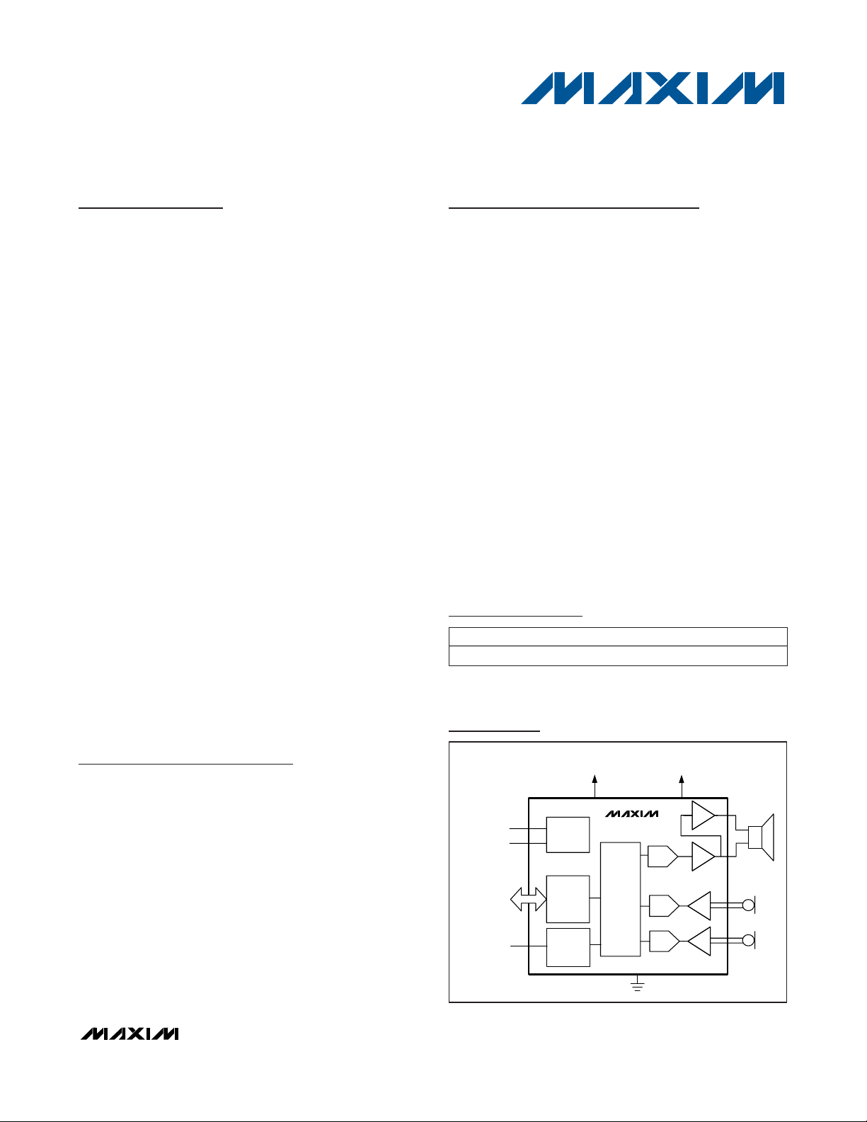
The MAX9860 is a low-power, voiceband, mono audio
codec designed to provide a complete audio solution
for wireless voice headsets and other mono voice audio
devices. Using an on-chip bridge-tied load mono headphone amplifier, the MAX9860 can output 30mW into a
32Ω earpiece while operating from a single 1.8V power
supply. Very low power consumption makes it an ideal
choice for battery-powered applications.
The MAX9860’s flexible clocking circuitry utilizes common system clock frequencies ranging from 10MHz to
60MHz, eliminating the need for an external PLL and
multiple crystal oscillators. Both the ADC and DAC support sample rates of 8kHz to 48kHz in either synchronous or asynchronous operation. Both master and slave
timing modes are supported.
Two differential microphone inputs are available with a
user-programmable preamplifier and programmable
gain amplifier. Automatic gain control with selectable
attack/release times and signal threshold allows maximum dynamic range. A noise gate with selectable
threshold provides a means to quiet the channel when
no signal is present. Both the DAC and ADC digital filters
provide full attenuation for out-of-band signals as well as
a 5th order GSM-compliant digital highpass filter. A digital side tone mixer provides loopback of the microphones/ADC signal to the DAC/headphone output.
Serial DAC and ADC data is transferred over a flexible
digital I2S-compatible interface that also supports TDM
mode. Mode settings, volume control, and shutdown are
programmed through a 2-wire, I
2
C-compatible interface.
The MAX9860 is fully specified over the -40°C to +85°C
extended temperature range and is available in a lowprofile, 4mm x 4mm, 24-pin thin QFN package.
Applications
Audio Headsets
Portable Navigation Device
Mobile Phones
Smart Phones
VoIP Phones
Audio Accessories
Features
♦ 1.8V Single-Supply Operation
♦ Digital Highpass Elliptical Filters with Notch for
217Hz (GSM)
♦ Mono 30mW BTL Headphone Amplifier
♦ Dual Low-Noise Microphone Inputs
♦ Automatic Microphone Gain Control and Noise
Gate
♦ 90dB DAC DR (f
S
= 48kHz)
♦ 81dB ADC DR (f
S
= 48kHz)
♦ Supports Master Clock Frequencies from 10MHz
to 60MHz
♦ Supports Sample Rates from 8kHz to 48kHz
♦ Flexible Digital Audio Interface
♦ Clickless/Popless Operation
♦ 2-Wire, I
2
C-Compatible Control Interface
♦ Available in 24-Pin, Thin QFN, 4mm x 4mm x
0.8mm Package
MAX9860
16-Bit Mono Audio Voice Codec
________________________________________________________________
Maxim Integrated Products
1
19-4349; Rev 0; 10/08
For pricing, delivery, and ordering information, please contact Maxim Direct at 1-888-629-4642,
or visit Maxim’s website at www.maxim-ic.com.
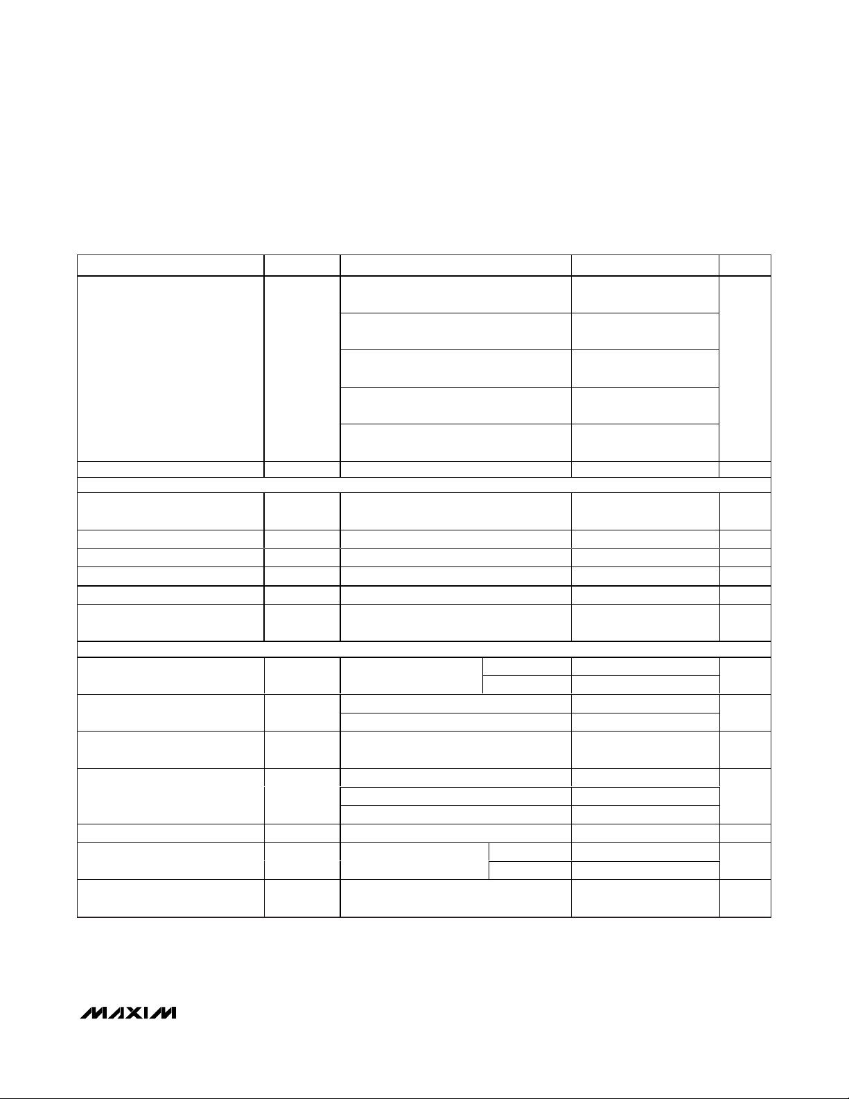
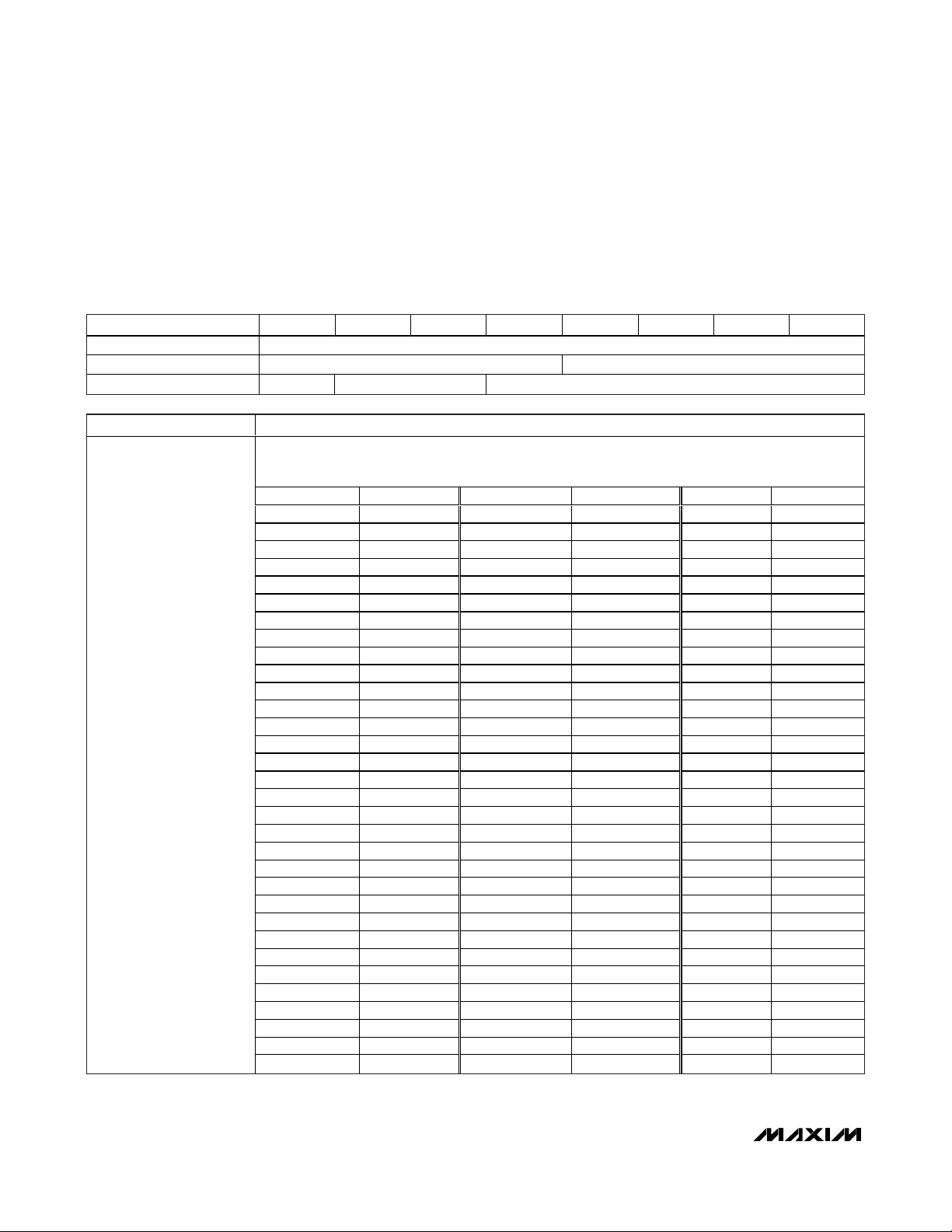
Ordering Information
+
Denotes a lead-free/RoHS-compliant package.
*
EP = Exposed pad.
ADC
ADC
DIGITAL
AUDIO
INTERFACE
DIGITAL
FILTERING
AND
MIXERS
DIFF
MIC
DIFF
MIC
DAC
AVDD AND DVDD
1.7V TO 1.9V
DVDDIO
1.7V TO 3.6V
CLOCK
CONTROL
DIGITAL AUDIO
INPUT/OUTPUT
I
2
C
INTERFACE
MAX9860
Simplified Block Diagram
Pin Configuration and Typical Operating Circuit appear at
end of data sheet.
PART TEMP RANGE PIN-PACKAGE
MAX9860ETG+ -40°C to +85°C 24 TQFN-EP*
Page 2
MAX9860
16-Bit Mono Audio Voice Codec
2 _______________________________________________________________________________________
ABSOLUTE MAXIMUM RATINGS
ELECTRICAL CHARACTERISTICS
(V
AVDD
= V
DVDD
= V
DVDDIO
= +1.8V, RL= ∞, headphone load (RL) connected between OUTP and OUTN, C
REF
= 2.2µF, C
MICBIAS
=
C
PREG
= C
REG
= 1µF, A
VPRE
= +20dB, A
VMICPGA
= 0dB, MCLK = 13MHz, LRCLK = 8kHz, TA= T
MIN
to T
MAX
, unless otherwise noted.
Typical values are at T
A
= +25°C.) (Note 2)
Stresses beyond those listed under “Absolute Maximum Ratings” may cause permanent damage to the device. These are stress ratings only, and functional
operation of the device at these or any other conditions beyond those indicated in the operational sections of the specifications is not implied. Exposure to
absolute maximum rating conditions for extended periods may affect device reliability.
(Voltages referenced to AGND.)
DVDDIO, SDA, SCL, IRQ.......................................-0.3V to +3.6V
AVDD, DVDD............................................................-0.3V to +2V
AGND, DGND, MICGND .......................................-0.3V to +0.3V
OUTP, OUTN, PREG, REF, MICBIAS ......-0.3V to (AVDD + 0.3V)
MICLP, MICLN, MICRP, MICRN, REG ....-0.3V to (PREG + 0.3V)
MCLK, LRCLK, BCLK,
SDOUT, SDIN..................................-0.3V to (DVDDIO + 0.3V)
Continuous Power Dissipation (T
A
= +70°C)
24-Pin TQFN (derate 27.8mW/°C above +70°C,
multilayer board) ......................................................2222mW
Junction-to-Ambient Thermal Resistance (θ
JA
) (Note 1)
24-Pin TQFN (derate 27.8mW/°C above +70°C,
multilayer board) ........................................................36°C/W
Operating Temperature Range ...........................-40°C to +85°C
Storage Temperature Range .............................-65°C to +150°C
Lead Temperature (soldering, 10s) .................................+300°C
Note 1: Package thermal resistances were obtained using the method described in JEDEC specification JESD51-7, using a four-layer
board. For detailed information on package thermal considerations, refer to www.maxim-ic.com/thermal-tutorial
.
Supply Voltage Range
Total Supply Current
(Note 3)
Shutdown Supply Current I
Shutdown to Full Operation 10 ms
DAC (Note 4)
Gain Error ±1 ±5 %
Dynamic Range (Note 5) DR
DAC Full-Scale Output 1V
DAC Path Phase Delay
Total Harmonic Distortion + Noise THD+N
PARAMETER SYMBOL CONDITIONS MIN TYP MAX UNITS
I
AVDD+DVDD
SHDN
AVDD (inferred from HP output PSRR) 1.7 1.8 1.9
DVDD (inferred from codec performance
tests)
DVDDIO 1.7 1.8 3.6
DAC playback mode
(48kHz)
Full operation
8kHz mono ADC + DAC
Full operation
8kHz stereo ADC + DAC
Stereo ADC only (48kHz)
TA = +25°C
+0dB volume setting, f
measured at headphone output,
T
= +25°C
A
f = 1kHz, 0dBFS, HP
filter disabled, digital
input to analog output
f = 1kHz, MCLK = 12.288MHz,
LRCLK = 48kHz
AVDD 1.46 2.2
DVDD 1.05 1.6
AVDD 4.08 5.7
DVDD 0.78 1.0
AVDD 6.17 9.0
DVDD 0.8 1.2
AVDD 5.38 8.0
DVDD 1.68 2.2
AVDD 0.56 5
DVDD +
DVDDIO
= 8kHz,
S
fS = 8kHz 1.2
f
= 16kHz 0.59
S
1.7 1.8 1.9
84 90 dB
V
mA
1.65 5
-87 dB
µA
RMS
ms
Page 3
MAX9860
16-Bit Mono Audio Voice Codec
_______________________________________________________________________________________ 3
ELECTRICAL CHARACTERISTICS (continued)
(V
AVDD
= V
DVDD
= V
DVDDIO
= +1.8V, RL= ∞, headphone load (RL) connected between OUTP and OUTN, C
REF
= 2.2µF, C
MICBIAS
=
C
PREG
= C
REG
= 1µF, A
VPRE
= +20dB, A
VMICPGA
= 0dB, MCLK = 13MHz, LRCLK = 8kHz, TA= T
MIN
to T
MAX
, unless otherwise noted.
Typical values are at T
A
= +25°C.) (Note 2)
PARAMETER SYMBOL CONDITIONS MIN TYP MAX UNITS
Power-Supply Rejection Ratio PSRR
f = 1kHz, V
A
= 0dB
VPGA
f = 10kHz, V
A
= 0dB
VPGA
RIPPLE
RIPPLE
= 100mV
= 100mV
P-P
P-P
,
,
94
71
DAC LOWPASS DIGITAL FILTER
Passband Cutoff f
PLP
With respect to fS within ripple; fS = 8kHz
to 48kHz
0.448 x
f
S
-3dB cutoff 0.451 f
Passband Ripple f < f
Stopband Cutoff f
SLP
With respect to fS; fS = 8kHz to 48kHz
Stopband Attenuation f > f
PLP
, f = 20Hz to 20kHz 75 dB
SLP
±0.1 dB
0.476 x
f
S
DAC HIGHPASS DIGITAL FILTER
5th Order Passband Cutoff
(-3dB from Peak, I
2
C Register
f
DHPPB
Programmable) (Note 6)
5th Order Stopband Cutoff
(-30dB from Peak, I
C Register
f
DHPSB
2
Programmable) (Note 6)
DC Blocking DC
Atten
DVFLT = 0x1
(elliptical for 16kHz GSM)
DVFLT = 0x2
(500Hz Butterworth for 16kHz)
DVFLT = 0x3
(elliptical for 8kHz GSM)
DVFLT = 0x4
(500Hz Butterworth for 8kHz)
DVFLT = 0x5
(200Hz Butterworth for 48kHz)
DVFLT = 0x1
(elliptical for 16kHz GSM)
DVFLT = 0x2
(500Hz Butterworth for 16kHz)
DVFLT = 0x3
(elliptical for 8kHz GSM)
DVFLT = 0x4
(500Hz Butterworth for 8kHz)
DVFLT = 0x5
(200Hz Butterworth for 48kHz)
DVFLT ≠ 0x0 90 dB
0.0161
x f
S
0.0312
x f
S
0.0321
x f
S
0.0625
x f
S
0.0042
x f
S
0.0139
x f
S
0.0156
x f
S
0.0279
x f
S
0.0312
x f
S
0.0021
x f
S
ADC
Full-Scale Input Voltage 0dBFS
Differential MIC Input, A
A
= 0dB
VPGA
VPRE
= 0dB,
1V
Channel Gain Mismatch ±0.3 %
dB
Hz
S
Hz
Hz
Hz
P-P
Page 4
MAX9860
16-Bit Mono Audio Voice Codec
4 _______________________________________________________________________________________
ELECTRICAL CHARACTERISTICS (continued)
(V
AVDD
= V
DVDD
= V
DVDDIO
= +1.8V, RL= ∞, headphone load (RL) connected between OUTP and OUTN, C
REF
= 2.2µF, C
MICBIAS
=
C
PREG
= C
REG
= 1µF, A
VPRE
= +20dB, A
VMICPGA
= 0dB, MCLK = 13MHz, LRCLK = 8kHz, TA= T
MIN
to T
MAX
, unless otherwise noted.
Typical values are at T
A
= +25°C.) (Note 2)
PARAMETER SYMBOL CONDITIONS MIN TYP MAX UNITS
Dynamic Range (Note 5) DR
ADC Phase Delay
fS = 8kHz, A
A-weighted from 20Hz to f
= 48kHz, A
f
S
f = 1kHz, 0dBFS, HP filter
disabled, analog input to
digital output
= 0dB,
VPRE
= 0dB, TA = +25°C 75 83
VPRE
/2
S
fS = 8kHz 1.2
f
= 16kHz 0.61
S
81
Total Harmonic Distortion THD f = 1kHz, fS = 48kHz, TA = +25°C -70 -75 dB
Power-Supply Rejection Ratio PSRR
f = 1kHz, V
A
= 0dB
VPGA
f = 10kHz, V
A
= 0dB
VPGA
RIPPLE
RIPPLE
= 100mV
= 100mV
P-P
P-P
,
,
82
76
Channel Crosstalk Driven channel at -1dBFS, f = 1kHz -92 dB
ADC LOWPASS DIGITAL FILTER
Passband Cutoff f
PLP
With respect to fS within ripple;
f
= 8kHz to 48kHz
S
0.445 x
f
S
-3dB cutoff 0.449 f
Passband Ripple f < f
Stopband Cutoff f
SLP
With respect to fS; fS = 8kHz to 48kHz
Stopband Attenuation f > f
PLP
SLP
±0.1 dB
0.469 x
f
S
74 dB
ADC HIGHPASS DIGITAL FILTER
0.0161
x f
S
0.0312
x f
S
0.0321
x f
S
0.0625
x f
S
0.0042
x f
S
5th Order Passband Cutoff
2
(-3dB from Peak, I
C Register
Programmable) (Note 6)
f
AHPPB
AVFLT = 0x1 (elliptical for 16kHz GSM)
AVFLT = 0x2 (500Hz Butterworth for
16kHz)
AVFLT = 0x3 (elliptical for 8kHz GSM)
AVFLT = 0x4
(500Hz Butterworth for 8kHz)
AVFLT = 0x5
(200Hz Butterworth for 48kHz)
dB
ms
dB
Hz
Hz
Hz
S
Page 5
MAX9860
16-Bit Mono Audio Voice Codec
_______________________________________________________________________________________ 5
ELECTRICAL CHARACTERISTICS (continued)
(V
AVDD
= V
DVDD
= V
DVDDIO
= +1.8V, RL= ∞, headphone load (RL) connected between OUTP and OUTN, C
REF
= 2.2µF, C
MICBIAS
=
C
PREG
= C
REG
= 1µF, A
VPRE
= +20dB, A
VMICPGA
= 0dB, MCLK = 13MHz, LRCLK = 8kHz, TA= T
MIN
to T
MAX
, unless otherwise noted.
Typical values are at T
A
= +25°C.) (Note 2)
PARAMETER SYMBOL CONDITIONS MIN TYP MAX UNITS
5th Order Stopband Cutoff
(-30dB from peak, I
2
C Register
Programmable) (Note 6)
DC Blocking DC
f
AHPSB
ATTEN
AVFLT = 0x1
(elliptical for 16kHz GSM)
AVFLT = 0x2
(500Hz Butterworth for 16kHz)
AVFLT = 0x3
(elliptical for 8kHz GSM)
AVFLT = 0x4
(500Hz Butterworth for 8kHz)
AVFLT = 0x5
(200Hz Butterworth for 48kHz)
AVFLT ≠ 0x0 90 dB
0.0139
x f
S
0.0156
x f
S
0.0279
x f
S
0.0312
x f
S
0.0021
x f
S
CLOCKING
MCLK Input Frequency
MCLK is not required to be synchronous
or related to the desired LRCLK data rate
10 60 MHz
MCLK Duty Cycle 40 50 60 %
Maximum MCLK Input Jitter For guaranteed performance limits 100 ps
LRCLK Data Rate Frequency 8 48 kHz
LRCLK PLL Lock Time 12 25 ms
LRCLK Acceptable Jitter for
Maintaining PLL Lock
±20 ns
MONO HEADPHONE AMPLIFIER
Output Power P
OUT
Total Harmonic Distortion + Noise THD+N
Dynamic Range (Note 5) DR
f = 1kHz, THD+N ≤ 1%
T
= +25°C
A
RL = 32Ω, P
= 16Ω, P
R
L
= 25mW, f = 1kHz 0.05
OUT
= 25mW, f = 1kHz 0.08
OUT
+0dB volume setting, DAC input at
= 8kHz to 48kHz
f
S
RL = 16Ω 30 50
R
= 32Ω 33
L
90 dB
AVDD = 1.7V to 1.9V 60 84
V
= 100mV
RIPPLE
= 100mV
V
RIPPLE
Output Offset Voltage V
OS
V
OUTP
- V
OUTN, TA
Capacitive Drive Capability No sustained oscillations
Click-and-Pop Level
Peak voltage into/out of shutdown, 32sps,
A-weighted
, f = 217Hz 86Power-Supply Rejection Ratio PSRR
P-P
, f = 20kHz 71
P-P
=+25°C ± 0.25 ± 1 mV
RL = 32Ω 500
R
= ∞ 100
L
-70 dBV
Hz
RMS
mW
%
dB
pF
Page 6
MAX9860
16-Bit Mono Audio Voice Codec
6 _______________________________________________________________________________________
ELECTRICAL CHARACTERISTICS (continued)
(V
AVDD
= V
DVDD
= V
DVDDIO
= +1.8V, RL= ∞, headphone load (RL) connected between OUTP and OUTN, C
REF
= 2.2µF, C
MICBIAS
=
C
PREG
= C
REG
= 1µF, A
VPRE
= +20dB, A
VMICPGA
= 0dB, MCLK = 13MHz, LRCLK = 8kHz, TA= T
MIN
to T
MAX
, unless otherwise noted.
Typical values are at T
A
= +25°C.) (Note 2)
PARAMETER SYMBOL CONDITIONS MIN TYP MAX UNITS
MICROPHONE AMPLIFIER
PAM = 00 Off
Preamplifier Gain A
VPRE
TA = +25°C
PAM = 01 -0.5 0 +0.5
PAM = 10 19 20 21
dB
PAM = 11 29 30 31
MIC PGA Gain A
VMICPGA
PGAM = 0x14–0x1F 0
PGAM = 0x00 +20
dB
MIC PGA Gain Step Size 1dB
Common-Mode Rejection Ratio CMRR VIN = 100mV
MIC Input Resistance R
IN_MIC
All gain settings, measured at
MICLN/MICRN
at 217Hz 50 dB
P-P
30 50 kΩ
MIC Input Bias Voltage 0.7 0.8 0.9 V
A
Total Harmonic Distortion + Noise THD+N
MIC Power-Supply Rejection
Ratio
PSRR
= 0dB, A
V
A
V
VPRE
IN
VPRE
IN
= 1V
= 31mV
= +30dB, A
, f = 1kHz
P-P
P-P
VMICPGA
, f = 1kHz
AVDD = 1.7V to 1.9V 60 95 dB
V
= 100mV at 1kHz, input referred 82 dB
RIPPLE
V
= 100mV at 10kHz, input referred 76 dB
RIPPLE
= 0dB,
VMICPGA
= 0dB,
-75 dB
-66 dB
MICROPHONE BIAS
MICBIAS Output Voltage V
MICBIASILOAD
Load Regulation I
MICBIAS Line Ripple Rejection LRR
MICBIAS Noise Voltage A-weighted 9.5 µV
= 1mA, TA = +25°C 1.5 1.55 1.6 V
= 1mA to 2mA 0.2 10 mV
LOAD
V
RIPPLE
V
RIPPLE
= 100mV
= 100mV
at 217Hz 82 dB
P-P
at 10kHz 81 dB
P-P
RMS
AUTOMATIC GAIN CONTROL
AGC Hold Duration AGCHLD[1:0] setting range, FREQ ≠ 0 50 400 ms
AGC Attack Time AGCATK[1:0] setting range, FREQ ≠ 0 3 200 ms
AGC Release Time AGCRLS[2:0] setting range, FREQ ≠ 0 0.078 10 s
AGC Threshold Level AGCSTH[3:0] setting range, FREQ ≠ 0 -3 -18 dB
NOISE GATE
NG Attack and Release Time 0.5 s
NG Threshold Level -72 -16 dB
Noise Gate Threshold Step Size 4dB
NG Attenuation 012dB
DIGITAL SIDETONE
Sidetone Gain Adjust DVST 2dB steps -60 0 dB
Sidetone Phase Delay PDLY
MIC input to headphone
output, f = 1kHz, HP filter
disabled
8kHz 2.2
ms
16kHz 1.1
Page 7
MAX9860
16-Bit Mono Audio Voice Codec
_______________________________________________________________________________________ 7
DIGITAL AUDIO INTERFACE ELECTRICAL CHARACTERISTICS
(V
DVDD
= V
DVDDIO
= 1.8V, unless otherwise noted.) (Note 2)
I2C INTERFACE ELECTRICAL CHARACTERISTICS
(V
DVDD
= V
DVDDIO
= 1.8V, unless otherwise noted.) (Note 2)
PARAMETER SYMBOL CONDITIONS MIN TYP MAX UNITS
BCLK Cycle Time t
BCLK High Time t
BCLK Low Time t
BCLK or LRCLK Rise and Fall
Time
SDIN or LRCLK to BCLK Rising
Setup Time
SDIN or LRCLK to BCLK Falling
Setup Time
SDIN or LRCLK to BCLK Rising
Hold Time
SDIN or LRCLK to BCLK Falling
Hold Time
SDOUT Delay Time from BCLK
Rising Edge
BCLKS
BCLKH
BCLKL
t
, t
R
F
t
SU
t
SU
t
HD
t
HD
t
DLY
Slave operation 75 ns
Slave operation 30 ns
Slave operation 30 ns
Master operation 7 ns
ABCI = DBCI = 0 25 ns
ABCI = DBCI = 1 25 ns
ABCI = DBCI = 0 0 ns
ABCI = DBCI = 1 0 ns
ABCI = DBCI = 0, CL = 30pF 0 40 ns
PARAMETER SYMBOL CONDITIONS MIN TYP MAX UNITS
Serial-Clock Frequency f
Bus Free Time Between STOP
and START Conditions
Hold Time (Repeated) START
Condition
t
SCL Pulse Width Low t
SCL Pulse Width High t
Setup Time for a Repeated
START Condition
t
Data Hold Time t
Data Setup Time t
SDA and SCL Receiving
Rise Time
SDA and SCL Receiving
Fall Time
SCL
t
BUF
HD,STA
LOW
HIGH
SU,STA
HD,DAT
SU,DAT
t
R
t
F
CB is in pF 20 + 0.1C
CB is in pF 20 + 0.1C
0 400 kHz
1.3 µs
0.6 µs
1.3 µs
0.6 µs
0.6 µs
0 900 ns
100 ns
B
B
300 ns
300 ns
Page 8
MAX9860
16-Bit Mono Audio Voice Codec
8 _______________________________________________________________________________________
Note 2: All devices are 100% production tested at room temperature. All temperature limits are guaranteed by design.
Note 3: Supply current measurements taken with no applied signal at microphone inputs. A digital zero audio signal used for all dig-
ital serial audio inputs. Headphone outputs are loaded as stated in the global conditions.
Note 4: DAC performance is measured at headphone outputs.
Note 5: ADC, DAC, and headphone amplifier dynamic ranges are measured using the EIAJ method. -60dBV 1kHz input signal, A-weight-
ed and normalized to 0dBFS.
Note 6: Notch for GSM filters occurs at 217Hz.
I2C INTERFACE ELECTRICAL CHARACTERISTICS (continued)
(V
DVDD
= V
DVDDIO
= 1.8V, unless otherwise noted.) (Note 2)
SDA Transmitting
Fall Time
Setup Time for STOP Condition t
Bus Capacitance C
Pulse Width of Suppressed Spike t
DIGITAL INPUTS (LRCLK, BCLK, SDIN, MCLK)
Input Voltage High V
Input Voltage Low V
MCLK Input Voltage High 1.4 V
MCLK Input Voltage Low 0.4 V
Input Leakage Current IIH, I
Input Capacitance 3pF
DIGITAL INPUTS (SCL, SDA)
Input Voltage High V
Input Voltage Low V
Input Hysteresis 200 mV
Input Leakage Current IIH, I
Input Capacitance 3pF
CMOS DIGITAL OUTPUTS (BCLK, LRCLK, SDOUT)
Output Low Voltage V
Output High Voltage V
OPEN-DRAIN DIGITAL OUTPUTS (SDA, IRQ)
Output High Leakage Current I
Output Low Voltage V
PARAMETER SYMBOL CONDITIONS MIN TYP MAX UNITS
t
SU,STO
SP
OL
OH
OH
OL
CB is in pF 20 + 0.1C
F
B
IH
IL
TA = +25°C -1 +1 µA
IL
IH
IL
TA = +25oC-1+1µA
IL
IOL = 3mA 0.4 V
IOL = 3mA
V
= DVDDIO, TA = +25°C -1 +1 µA
OUT
IOL = 3mA 0.4 V
x DVDDIO
x DVDD
DVDDIO
B
0.6 µs
050ns
0.7
0.7
- 0.4
250 ns
400 pF
0.3
x DVDDIO
0.3
x DVDD
V
V
V
V
V
Page 9
MAX9860
16-Bit Mono Audio Voice Codec
_______________________________________________________________________________________
9
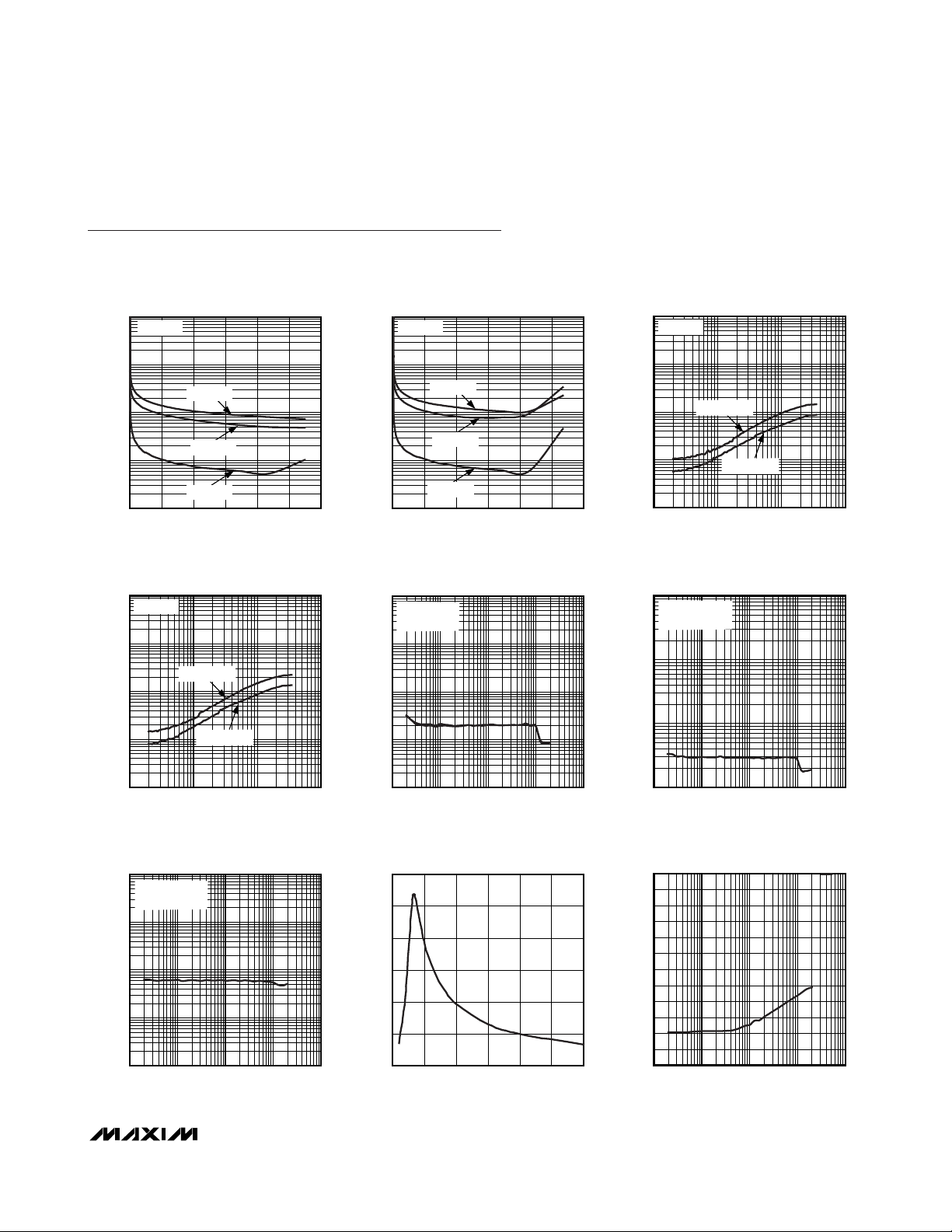
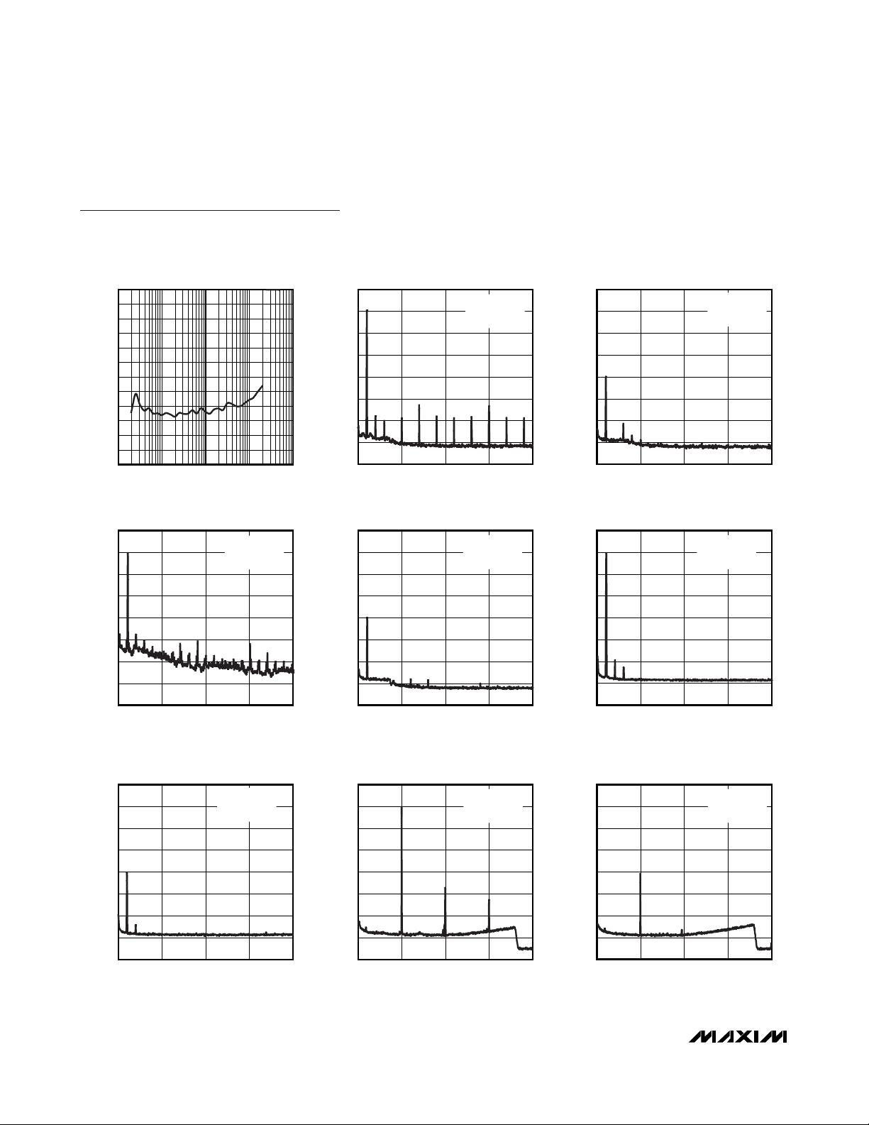
Typical Operating Characteristics
(V
AVDD
= +1.8V, V
DVDD
= V
DVDDIO
= +1.8V, RL= ∞, headphone load (RL) connected between OUTP and OUTN, C
REF
= 2.2µF,
C
PREG
= C
REG
= 1µF, C
MICBIAS
= 1µF A
VMICPGA
= 0dB, A
VPRE
= +20dB, MCLK = 13MHz, TA= +25°C, unless otherwise noted.)
TOTAL HARMONIC DISTORTION + NOISE
TOTAL HARMONIC DISTORTION + NOISE
vs. OUTPUT POWER (DAC TO HP)
10
RL = 32Ω
1
f = 3.5kHz
0.1
THD+N (%)
0.01
0.001
030
f = 1kHz
f = 20kHz
252015105
OUTPUT POWER (mW)
TOTAL HARMONIC DISTORTION + NOISE
MAX9860 toc01
10
RL = 16Ω
1
0.1
THD+N (%)
0.01
0.001
060
TOTAL HARMONIC DISTORTION + NOISE
vs. FREQUENCY (DAC TO HP)
10
1
0.1
THD+N (%)
0.01
RL = 16Ω
P
= 5mW
OUT
P
= 20mW
OUT
MAX9860 toc04
10
1
0.1
THD+N (%)
0.01
MICPRE = 0dB
V
IN
vs. OUTPUT POWER (DAC TO HP)
f = 3.5kHz
f = 1kHz
f = 20kHz
5040302010
OUTPUT POWER (mW)
vs. FREQUENCY (MICL TO ADC)
= 1V
P-P
MAX9860 toc02
MAX9860 toc05
TOTAL HARMONIC DISTORTION + NOISE
vs. FREQUENCY (DAC TO HP)
10
RL = 32Ω
1
P
= 5mW
0.1
THD+N (%)
0.01
0.001
0.01 10
OUT
P
= 20mW
OUT
FREQUENCY (kHz)
10.1
TOTAL HARMONIC DISTORTION + NOISE
vs. FREQUENCY (MICL TO ADC)
10
MICPRE = +20dB
= 100mV
V
IN
P-P
1
THD+N (%)
0.1
MAX9860 toc03
MAX9860 toc06
0.001
0.01 10
FREQUENCY (kHz)
10.1
TOTAL HARMONIC DISTORTION + NOISE
vs. FREQUENCY (MICL TO ADC)
10
MICPRE = +30dB
= 31V
V
IN
P-P
1
0.1
THD+N (%)
0.01
0.001
0.01 100
FREQUENCY (kHz)
MAX9860 toc08
0.01
0.01 100
FREQUENCY (kHz)
POWER-SUPPLY REJECTION RATIO
vs. FREQUENCY (DAC TO HP)
0
-10
-20
-30
-40
-50
-60
PSRR (dB)
-70
-80
-90
-100
-110
-120
0.01 100
FREQUENCY (kHz)
1010.1
MAX9860 toc09
1010.1
0.001
0.01 100
FREQUENCY (kHz)
1010.1
HEADPHONE OUTPUT POWER
vs. LOAD RESISTANCE
60
50
MAX9860 toc07
40
30
20
OUTPUT POWER (mW)
10
0
1010.1
0 150
LOAD RESISTANCE (Ω)
125100755025
Page 10
MAX9860
16-Bit Mono Audio Voice Codec
10 ______________________________________________________________________________________
Typical Operating Characteristics (continued)
(V
AVDD
= +1.8V, V
DVDD
= V
DVDDIO
= +1.8V, RL= ∞, headphone load (RL) connected between OUTP and OUTN, C
REF
= 2.2µF,
C
PREG
= C
REG
= 1µF, C
MICBIAS
= 1µF A
VMICPGA
= 0dB, A
VPRE
= +20dB, MCLK = 13MHz, TA= +25°C, unless otherwise noted.)
POWER-SUPPLY REJECTION RATIO
vs. FREQUENCY (MIC TO ADC)
0
-10
-20
-30
-40
-50
-60
PSRR (dB)
-70
-80
-90
-100
-110
-120
0.01 100
FREQUENCY (kHz)
0dBFS FFT (DAC TO HP)
20
MAX9860 toc10
1010.1
0
-20
-40
-60
-80
OUTPUT AMPLITUDE (dB)
-100
-120
-140
020
FREQUENCY (kHz)
MCLK = 13MHz
LRCLK = 8kHz
PLL DISABLED
15105
20
MAX9860 toc11
0
-20
-40
-60
-80
OUTPUT AMPLITUDE (dB)
-100
-120
-140
-60dBFS FFT (DAC TO HP)
MCLK = 13MHz
LRCLK = 8kHz
PLL DISABLED
020
FREQUENCY (kHz)
15105
MAX9860 toc12
20
0
-20
-40
-60
-80
OUTPUT AMPLITUDE (dB)
-100
-120
-140
020
FREQUENCY (kHz)
MCLK = 13MHz
LRCLK = 8kHz
PLL ENABLED
15105
20
MAX9860 toc13
0
-20
-40
-60
-80
OUTPUT AMPLITUDE (dB)
-100
-120
-140
-60dBFS FFT (DAC TO HP AMP)
0dBFS FFT (DAC TO HP)
20
0
-20
-40
-60
-80
OUTPUT AMPLITUDE (dB)
-100
-120
-140
020
FREQUENCY (kHz)
MCLK = 12.288MHz
LRCLK = 48kHz
PLL DISABLED
15105
20
MAX9860 toc16
0
-20
-40
-60
-80
OUTPUT AMPLITUDE (dB)
-100
-120
-140
-60dBFS FFT (DAC TO HP)
020
0dBFS FFT (MICL TO ADC)
04
FREQUENCY (kHz)
FREQUENCY (kHz)
MCLK = 13MHz
LRCLK = 8kHz
PLL ENABLED
15105
MCLK = 13MHz
LRCLK = 8kHz
PLL DISABLED
321
20
MAX9860 toc14
MAX9860 toc17
0
-20
-40
-60
-80
OUTPUT AMPLITUDE (dB)
-100
-120
-140
20
0
-20
-40
-60
-80
OUTPUT AMPLITUDE (dB)
-100
-120
-140
0dBFS FFT (DAC TO HP AMP)
MCLK = 12.288MHz
LRCLK = 48kHz
PLL DISABLED
020
FREQUENCY (kHz)
15105
MAX9860 toc15
-60dBFS FFT (MICL TO ADC)
MCLK = 13MHz
LRCLK = 8kHz
PLL DISABLED
04
FREQUENCY (kHz)
321
MAX9860 toc18
Page 11
MAX9860
16-Bit Mono Audio Voice Codec
______________________________________________________________________________________ 11
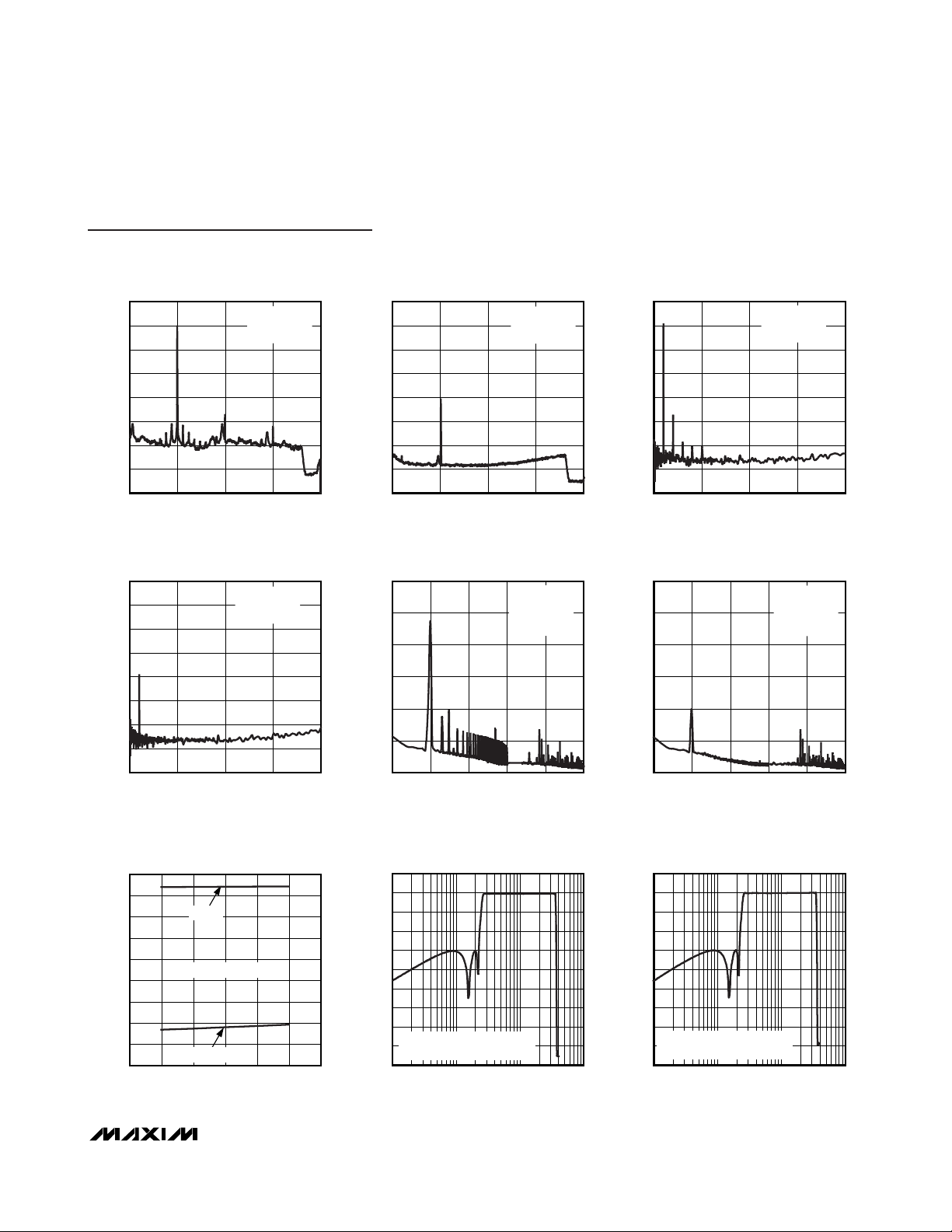
Typical Operating Characteristics (continued)
(V
AVDD
= +1.8V, V
DVDD
= V
DVDDIO
= +1.8V, RL= ∞, headphone load (RL) connected between OUTP and OUTN, C
REF
= 2.2µF,
C
PREG
= C
REG
= 1µF, C
MICBIAS
= 1µF A
VMICPGA
= 0dB, A
VPRE
= +20dB, MCLK = 13MHz, TA= +25°C, unless otherwise noted.)
0dBFS FFT (MICL TO ADC)
20
0
-20
-40
-60
-80
OUTPUT AMPLITUDE (dB)
-100
-120
-140
04
-60dBFS FFT (MICL TO ADC)
20
0
-20
-40
-60
-80
OUTPUT AMPLITUDE (dB)
-100
-120
-140
020
FREQUENCY (kHz)
MCLK = 12.288MHz
LRCLK = 48kHz
PLL DISABLED
FREQUENCY (kHz)
MCLK = 13MHz
LRCLK = 8kHz
PLL ENABLED
321
20
MAX9860 toc19
0
-20
-40
-60
-80
OUTPUT AMPLITUDE (dB)
-100
-120
-140
04
-5dBFS WIDEBAND FFT (DAC TO HP)
20
MAX9860 toc22
15105
0
-20
-40
-60
OUTPUT AMPLITUDE (dB)
-80
-100
0.1 10,000
-60dBFS FFT (MICL TO ADC)
MCLK = 13MHz
LRCLK = 8kHz
PLL ENABLED
321
FREQUENCY (kHz)
20
MAX9860 toc20
-20
-40
-60
-80
OUTPUT AMPLITUDE (dB)
-100
-120
-140
0dBFS FFT (MICL TO ADC)
0
020
FREQUENCY (kHz)
-60dBFS WIDEBAND FFT (DAC TO HP)
20
MAX9860 toc23
0
-20
-40
-60
OUTPUT AMPLITUDE (dB)
-80
-100
0.1 10,000
FREQUENCY (kHz)
FREQUENCY (kHz)
MCLK = 13MHz
LRCLK = 8kHz
PLL DISABLED
= 32Ω
R
L
1000100101
MCLK = 12.288MHz
LRCLK = 48kHz
PLL DISABLED
15105
MCLK = 13MHz
LRCLK = 8kHz
PLL DISABLED
= 32Ω
R
L
1000100101
MAX9860 toc21
MAX9860 toc24
SUPPLY CURRENT
vs. SUPPLY VOLTAGE
4.5
4.0
I
3.5
3.0
2.5
2.0
1.5
SUPPLY CURRENT (mA)
1.0
0.5
0
1.65 1.95
AVDD
FULL-DUPLEX 8kHz MODE
I
+ I
DVDD
DVDDIO
SUPPLY VOLTAGE (V)
DAC DIGITAL FILTER
FREQUENCY RESPONSE, 8kHz
10
0
MAX9860 toc25
-10
-20
-30
-40
-50
-60
OUTPUT AMPLITUDE (dBFS)
-70
ELLIPTICAL FOR 8kHz GSM WITH
-80
NOTCH AT 217Hz
-90
1.901.851.801.751.70
0.01 10
FREQUENCY (kHz)
10.1
10
0
MAX9860 toc26
-10
-20
-30
-40
-50
-60
OUTPUT AMPLITUDE (dBFS)
-70
-80
-90
0.01 10
ADC DIGITAL FILTER
FREQUENCY RESPONSE, 8kHz
ELLIPTICAL FOR 8kHz GSM WITH
NOTCH AT 217Hz
10.1
FREQUENCY (kHz)
MAX9860 toc27
Page 12
MAX9860
16-Bit Mono Audio Voice Codec
12 ______________________________________________________________________________________
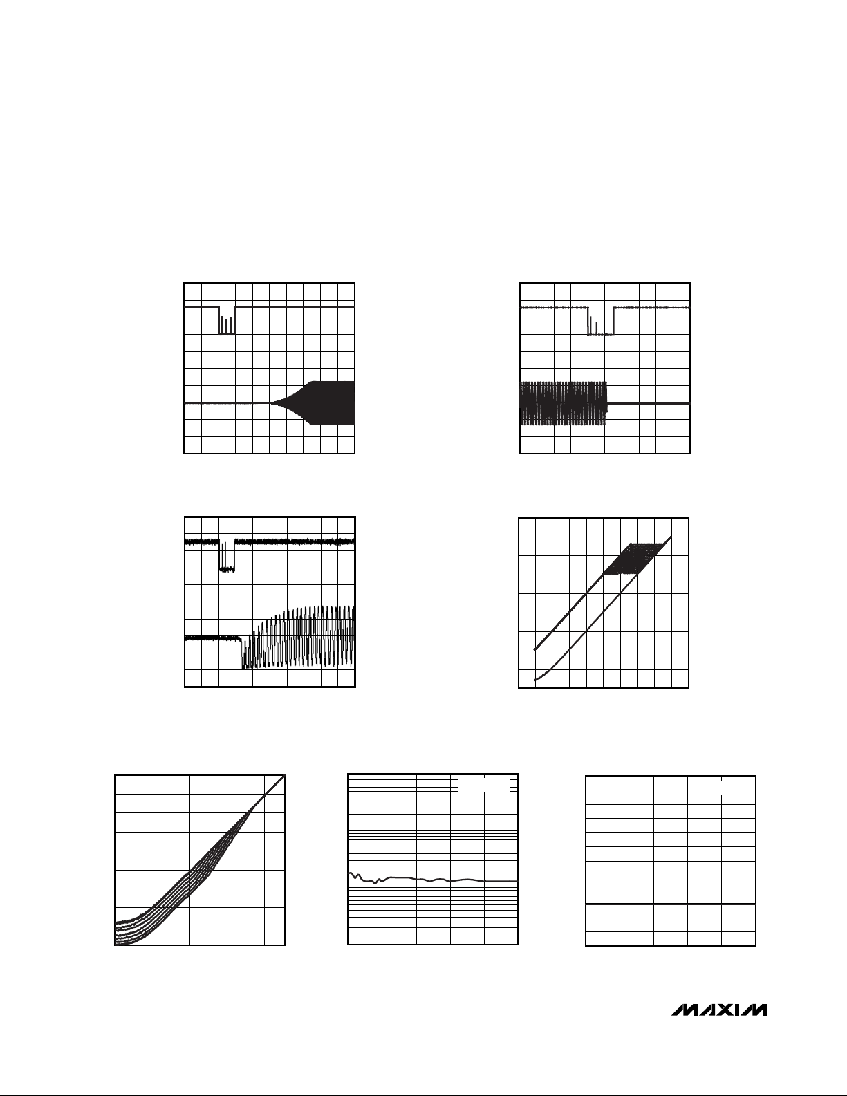
Typical Operating Characteristics (continued)
(V
AVDD
= +1.8V, V
DVDD
= V
DVDDIO
= +1.8V, RL= ∞, headphone load (RL) connected between OUTP and OUTN, C
REF
= 2.2µF,
C
PREG
= C
REG
= 1µF, C
MICBIAS
= 1µF A
VMICPGA
= 0dB, A
VPRE
= +20dB, MCLK = 13MHz, TA= +25°C, unless otherwise noted.)
HEADPHONE STARTUP WAVEFORM
MAX9860 toc28
TIME (4ms/div)
SPK+ -SPK-
(1V/div)
SDA
(2V/div)
HEADPHONE SHUTDOWN WAVEFORM
MAX9860 toc29
TIME (2ms/div)
SPK+ -SPK-
(1V/div)
SDA
(2V/div)
ADC OUTPUT
(500mV/div)
SDA
(2V/div)
SOFT-START ADC
MAX9860 toc30
TIME (4ms/div)
-80
-60
-70
-40
-50
-30
-20
0
-10
10
-100 -80-90 -60-70 -40-50 -20-30 0-10
AUTOMATIC GAIN CONTROL THRESHOLDS
MAX9860 toc31
INPUT AMPLITUDE (dBV)
OUTPUT AMPLITUDE (dBFS)
-90
-70
-80
-50
-60
-40
-30
-10
-20
0
-100 -80 -60 -40 -20
NOISE GATE THRESHOLDS
MAX9860 toc32
INPUT AMPLITUDE (dBV)
OUTPUT AMPLITUDE (dBFS)
TOTAL HARMONIC DISTORTION + NOISE
vs. MCLK FREQUENCY, 0dBFS (DAC to HP)
MAX9860 toc33
MCLK FREQUENCY (MHz)
THD+N (%)
50403020
0.01
0.1
1
0.001
10 60
LRCLK = 8kHz
DYNAMIC RANGE
vs. MCLK FREQUENCY, -60dBFS (DAC to HP)
MAX9860 toc34
MCLK FREQUENCY (MHz)
DYNAMIC RANGE (dB)
50403020
-110
-100
-90
-80
-70
-60
-50
-40
-30
-20
-10
0
-120
10 60
LRCLK = 8kHz
Page 13

MAX9860
16-Bit Mono Audio Voice Codec
______________________________________________________________________________________ 13
Pin Description
PIN NAME FUNCTION
1 MICBIAS
2 REG Internal Bias. PREG/2 voltage reference. Bypass to AGND with a 1µF capacitor (+0.8V).
3 PREG Positive Internal Regulated Supply. Bypass to AGND with a 1µF capacitor (+1.6V).
4 REF Converter Reference (1.23V). Bypass to AGND with a 2.2µF capacitor.
5 AGND Analog Ground
6 AVDD Analog Power Supply. Bypass to AGND with 10µF and 0.1µF capacitors.
7 OUTP Positive Headphone Output
8 OUTN Negative Headphone Output
9 SDA I2C Serial-Data Input/Output
10 SCL I2C Serial-Data Clock
11 DVDDIO Digital Interface Power Supply. Supply for digital audio interface. Bypass to DGND with a 1µF capacitor.
12 DGND Digital Ground
13 DVDD Digital Core Power Supply. Bypass to DGND with a 1µF capacitor.
14 MCLK Master Clock Input
15 SDOUT Serial Audio Interface ADC Data Output
16 SDIN Serial Audio Interface DAC Data Input
17 LRCLK Serial Audio Interface Left/Right Clock
18 BCLK Serial Audio Interface Bit Clock
19 IRQ Interrupt Request. IRQ is an active-low open drain output. Pull up to DVDDIO with a 10kΩ resistor.
20 MICRN
21 MICRP
22 MICLN
23 MICLP
24 MICGND MICBIAS Ground. Connect to AGND.
— EP Exposed Pad. Connect to AGND.
Microphone Bias. +1.55V microphone bias for internal and/or external microphone. An external resistor from
2.2kΩ to 470Ω should be used to set the microphone current. Bypass to MICGND with a 1µF capacitor.
Negative Right Microphone Input. AC-couple to low-side of microphone or connect to negative signal.
AC-couple to ground for single-ended operation.
Positive Right Microphone Input. AC-couple to high-side of microphone or connect to positive signal.
AC-couple the signal for single-ended operation.
Negative Left Microphone Input. AC-couple to low-side of microphone or connect to negative signal.
AC-couple to ground for single-ended operation.
Positive Left Microphone Input. AC-couple to high-side of microphone or connect to positive signal.
AC-couple the signal for single-ended operation.
Page 14

MAX9860
Detailed Description
The MAX9860 is a low-power, voiceband, mono audio
codec designed to provide a complete audio solution
for wireless voice headsets and other mono audio
devices.
The mono playback path accepts digital audio over a
flexible digital audio interface compatible with I
2
S, TDM,
and left-justified audio signals. An oversampling sigmadelta DAC converts an incoming digital data stream to
analog audio and outputs through the mono bridge-tied
load headphone amplifier.
The stereo record path has two microphone inputs with
selectable gain. The microphones are powered by an
integrated microphone bias. An oversampling sigmadelta ADC converts the microphone signals and outputs the digital bit stream over the digital audio
interface.
The record path includes automatic gain control (AGC)
to optimize the signal level and a noise gate to reduce
idle noise. The automatic gain control monitors the outputs of the ADC and makes constant adjustments to the
input gain to reduce the dynamic range of the incoming
microphone signal by up to 20dB. The noise gate corrects for the increase in noise typically associated with
AGC by lowering the gain when there is no audio signal.
Integrated digital filtering provides a range of notch and
highpass filters for both the playback and record paths
to limit undesirable low-frequency signals and GSM
transmission noise. The digital filtering provides attenuation of out-of-band energy by up to 76dB, eliminating
audible aliasing. A digital sidetone function allows
audio from the record path to be summed into the playback path after digital filtering.
The MAX9860’s flexible clock circuitry utilizes a programmable clock divider and a digital PLL to allow the
DAC and ADC to operate at maximum dynamic range
for all combinations of master clock (MCLK) and sample rate (LRCLK). Any master clock between 10MHz to
60MHz is supported as are all sample rates from 8kHz
to 48kHz. Master and slave mode are supported for
maximum flexibility.
I
2
C Registers
The MAX9860 audio codec is completely controlled
through software using an I2C interface. The power-on
default setting is software shutdown, requiring that the
internal registers be programmed to activate the device.
See Table 1 for the device’s complete register map.
I2C Slave Address
The MAX9860 responds to the slave address 0x20 for
all write commands and 0x21 for all read operations.
16-Bit Mono Audio Voice Codec
14 ______________________________________________________________________________________
Page 15

MAX9860
16-Bit Mono Audio Voice Codec
______________________________________________________________________________________ 15
Table 1. I2C Register Map
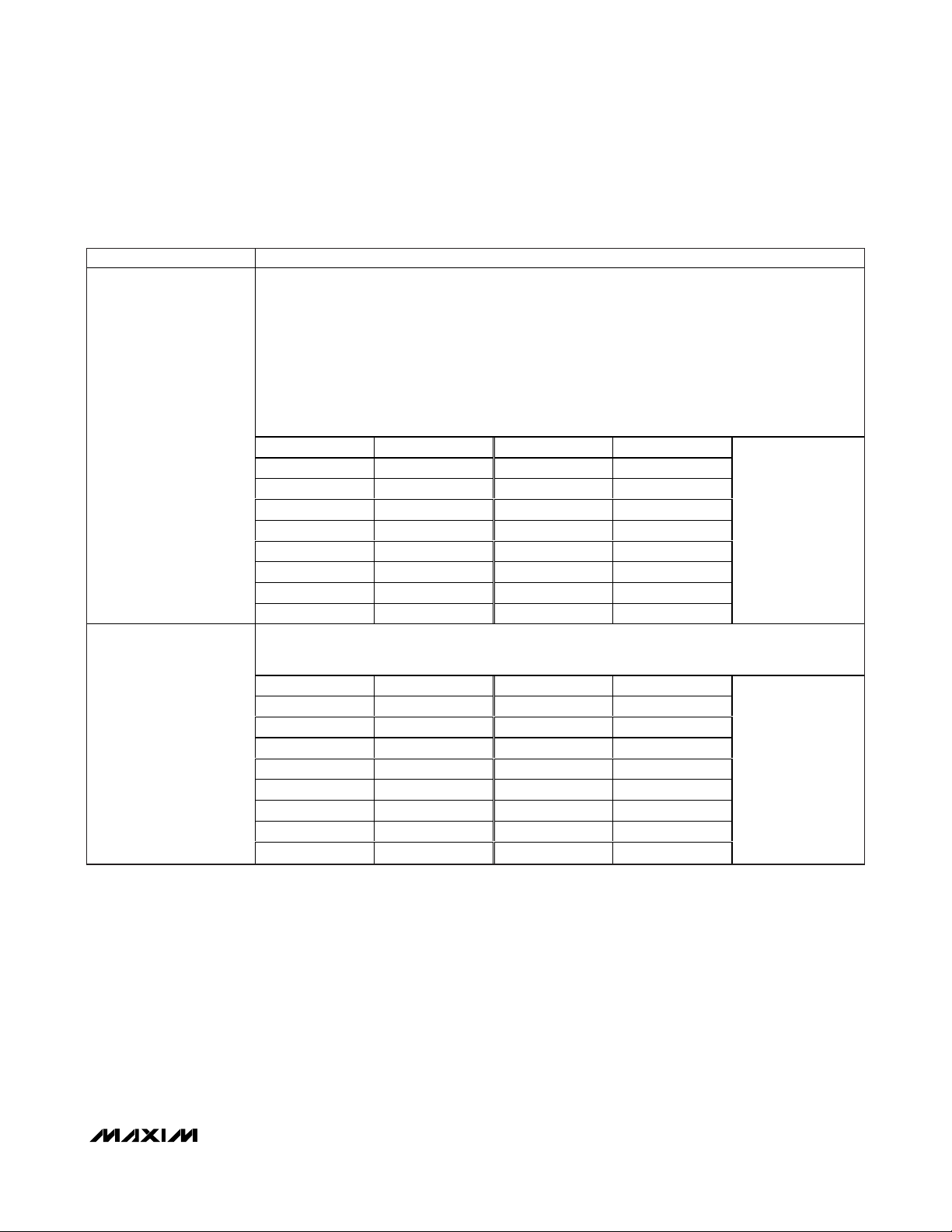
REGISTER B7 B6 B5 B4 B3 B2 B1 B0
STATUS/INTERRUPT
Interrupt Status CLD SLD ULK 0 0 0 0 0 0x00 — R
Microphone NG/AGC
Readback
Interrupt Enable ICLD ISLD IULK 0 0 0 0 0 0x02 0x00 R/W
CLOCK CONTROL
System Clock 0 0 PSCLK 0 FREQ 16KHZ 0x03 0x00 R/W
Stereo Audio Clock
Control High
Stereo Audio Clock
Control Low
DIGITAL AUDIO INTERFACE
Interface MAS WCI DBCI DDLY HIZ TDM 0 0 0x06 0x00 R/W
Interface 0 0 ABCI ADLY ST BSEL 0x07 0x00 R/W
DIGITAL FILTERING
Voice Filter AVFLT DVFLT 0x08 0x00 R/W
DIGITAL LEVEL CONTROL
DAC Attenuation DVA 0x09 0x00 R/W
ADC Output Levels ADCRL ADCLL 0x0A 0x00 R/W
DAC Gain and
Sidetone
MICROPHONE LEVEL CONTROL
Microphone Gain 0 PAM PGAM 0x0C 0x00 R/W
RESERVED
Reserved 0 0 0 0 0 0 0 0 0x0D 0x00
MICROPHONE AUTOMATIC GAIN CONTROL
Microphone AGC AGCSRC AGCRLS AGCATK AGCHLD 0x0E 0x00 R/W
Noise Gate,
Microphone AGC
POWER MANAGEMENT
System Shutdown SHDN 0 0 0 DACEN 0 ADCLEN ADCREN 0x10 0x00 R/W
PLL NHI 0x04 0x00 R/W
NG AGC 0x01 — R
NLO 0x05 0x00 R/W
0 DVG DVST 0x0B 0x00 R/W
ANTH AGCTH 0x0F 0x00 R/W
REGISTER
ADDRESS
POR R/W
Page 16

MAX9860
Status/Interrupt
Status registers 0x00 and 0x01 are read-only registers
that report the status of various device functions. The
status register bits are cleared upon a read operation of
the status register and are set the next time the event
occurs. Register 0x02 determines whether or not the status flags in register 0x00 simultaneously sets IRQ high.
16-Bit Mono Audio Voice Codec
16 ______________________________________________________________________________________
Table 2. Status/Interrupt Registers
REGISTER ADDRESS B7 B6 B5 B4 B3 B2 B1 B0
0x00 CLD SLD ULK 0 0 0 0 0
0x01 NG AGC
0x02 ICLD ISLD IULK 0 0 0 0 0
BITS FUNCTION
Clip Detect Flag. Indicates that a signal has become clipped in the ADC or DAC digital signal paths. CLD also
CLD
indicates that the AGC function, when enabled, has set the microphone PGA to 0dB and no further gain reduction
is possible.
SLD
ULK
NG
AGC
Slew Level Detect Flag. When volume or gain changes are made, the slewing circuitry smoothly steps through all
intermediate settings. When SLD is set high, all slewing has completed and the volume or gain is at its final value.
Digital PLL Unlock Flag. Indicates that the digital audio PLL for the ADC or DAC has become unlocked and digital
signal data is not reliable. When beginning operation in master mode, this flag goes high and can be cleared by
reading the status register.
Noise Gate Attenuation. When the noise gate is enabled these bits indicate the current noise gate attenuation.
Code Attenuation
000 0dB
001 1dB
010 2dB
011 3dB
100 6dB
101 8dB
110 10dB
111 12dB
AGC Gain. When the AGC is enabled these bits indicate the AGC controlled level to the MIC preamp. The levels
indicated by these bits correspond to the levels defined for the PGAM bits described in register 0x0C.
Page 17

Clock Control
The MAX9860 can work with a master clock (MCLK)
supplied from any system clock within the range of
10MHz to 60MHz. Internally, the MAX9860 requires a
10MHz to 20MHz clock so a prescaler divides by 1, 2,
or 4 to create the internal clock (PCLK). PCLK is used
to clock all portions of the MAX9860.
The MAX9860 is capable of supporting any sample rate
from 8kHz to 48kHz, including all common sample rates
(8kHz, 16kHz, 24kHz, 32kHz, 44.1kHz, 48kHz). To
accommodate a wide range of system architectures,
the MAX9860 supports three main clocking modes:
Normal Mode: This mode uses a 15-bit clock divider
coefficient to set the sample rate relative to the
prescaled MCLK input (PCLK). This allows high flexibility in both the MCLK and LRCLK frequencies and can
be used in either master or slave mode.
Exact Integer Mode: Common MCLK frequencies
(12MHz, 13MHz, and 19.2MHz) can be programmed to
operate in exact integer mode for both 8kHz and 16kHz
sample rates. In these modes, the MCLK and LRCLK
rates are selected by using the FREQ and 16KHZ bits
instead of the NHI, NLO, and PLL control bits.
PLL Mode: When operating in slave mode, a PLL can
be enabled to lock onto externally generated LRCLK
signals that are asynchronously related to PCLK.
MAX9860
16-Bit Mono Audio Voice Codec
______________________________________________________________________________________ 17
Table 3. Clock Control Registers
REGISTER ADDRESS B7 B6 B5 B4 B3 B2 B1 B0
0x03 0 0 PSCLK 0 FREQ 16KHZ
0x04 PLL NHI
0x05 NLO
BITS FUNCTION
MCLK Prescaler
Divides MCLK down to generate a PCLK between 10MHz and 20MHz.
PSCLK[1:0]
FREQ[1:0]
16KHZ
00 = Disable clock for low-power shutdown.
01 = Select if MCLK is between 10MHz and 20MHz.
10 = Select if MCLK is between 20MHz and 40MHz.
11 = Select if MCLK is greater than 40MHz.
Integer Clock Mode
Enables exact integer mode for three predefined PCLK frequencies. Exact integer mode is normally
intended for master mode, but can be enabled in slave mode if the externally supplied LRCLK exactly
matches the frequency specified in each mode.
00 = Normal operation (configure clocking with the PLL, NHI, and NLO bits).
01 = Select when PCLK is 12MHz (LRCLK = PCLK/1500 or PCLK/750).
10 = Select when PCLK is 13MHz (LRCLK = PCLK/1625 or PCLK/812.5).
11 = Select when PCLK is 19.2MHz (LRCLK = PCLK/2400 or PCLK/1200).
When FREQ ≠ 00, the PLL, NHI, and NLO bits are unused.
16kHz Mode
When FREQ ≠ 00:
0 = LRCLK is exactly 8kHz.
1 = LRCLK is exactly 16kHz.
When FREQ = 00, 16KHZ is used to set the AGC clock rate:
0 = Use when LRCLK ≤ 24kHz.
1 = Use when LRCLK > 24kHz.
Page 18

MAX9860
16-Bit Mono Audio Voice Codec
18 ______________________________________________________________________________________
Table 3. Clock Control Registers (continued)
Table 4. Common N Values
Note: Values in bold italics are exact integers that provide
maximum full-scale performance.
BITS FUNCTION
PLL Enable
0 = (Valid for slave and master mode)—The frequency of LRCLK is set by the NHI and NLO divider
bits. Set PLL = 0 in slave mode only if the externally generated LRCLK can be exactly selected
using the LRCLK divider.
PLL
NHI and NLO
1 = (Valid for slave mode only)—Used when the audio master generates an LRCLK not selectable
using the LRCLK divider. A digital PLL locks on to the externally supplied LRCLK signal
regardless of the MCLK frequency.
Rapid Lock Mode
To enable rapid lock mode set NHI and NLO to the nearest desired ratio and set NLO[0] = 1 (Register
0x05, bit 0) before setting the PLL mode bit.
LRCLK Divider
NHI and NLO control a 15-bit clock divider (N). When the PLL = 0 and FREQ = 00, the frequency of
LRCLK is determined by the clock divider. See Table 4 for common N values.
N = (65,536 x 96 x f
f
= LRCLK frequency
LRCLK
f
= prescaled MCLK internal clock frequency (PCLK)
PCLK
LRCLK
MCLK
(MHz)
11.2896 01 116A 22D4 45A9 6000 687D
12 01 1062 20C5 4189 5A51 624E
12.288 01 1000 2000 4000 5833 6000
13 01 F20 1E3F 3C7F 535F 5ABE
19.2 01 A3D 147B 28F6 3873 3D71
24 10 1062 20C5 4189 5A51 624E
26 10 F20 1E3F 3C7F 535F 5ABE
27 10 E90 1D21 3A41 5048 5762
PSCLK 8 16 32 44.1 48
LRCLK (kHz)
)/f
PCLK
Page 19

Digital Audio Interface
The MAX9860’s digital audio interface supports a wide
range of operating modes to ensure maximum compatibility. See Figures 1 through 4 for timing diagrams. In
master mode, the MAX9860 outputs LRCLK and BCLK,
while in slave mode, they are inputs. When operating in
master mode, BCLK can be configured in a number of
ways to ensure compatiblity with other audio devices.
MAX9860
16-Bit Mono Audio Voice Codec
______________________________________________________________________________________ 19
Table 5. Digital Audio Interface Registers
REGISTER ADDRESS B7 B6 B5 B4 B3 B2 B1 B0
0x06 MAS WCI DBCI DDLY HIZ TDM 0 0
0x07 0 0 ABCI ADLY ST BSEL
BITS FUNCTION
Master Mode
MAS
WCI
DBCI
DDLY
0 = The MAX9860 operates in slave mode with LRCLK and BCLK configured as inputs.
1 = The MAX9860 operates in master mode with LRCLK and BCLK configured as outputs.
LRCLK Invert
0 = Left-channel data is input and output while LRCLK is low.
1 = Right-channel data is input and output while LRCLK is low.
WCI is ignored when TDM = 1.
DAC BCLK Invert (must be set to ABCI)
In master and slave mode:
0 = SDIN is latched into the part on the rising edge of BCLK.
1 = SDIN is latched into the part on the falling edge of BCLK.
In master mode:
0 = LRCLK changes state following the rising edge of BCLK.
1 = LRCLK changes state following the falling edge of BCLK.
DAC Delay Mode
0 = SDIN data is latched on the first BCLK edge following an LRCLK edge.
1 = SDIN data is assumed to be delayed one BCLK cycle so that it is latched on the 2nd BCLK edge
following an LRCLK edge (I
2
S-compatible mode).
HIZ
TDM
ABCI
DDLY is ignored when TDM = 1.
SDOUT High-Impedance Mode
0 = SDOUT is set either high or low after all data bits have been transferred out of the part.
1 = SDOUT goes to a high-impedance state after all data bits have been transferred out of the part,
allowing SDOUT to be shared by other devices.
Use HIZ only when TDM = 1.
TDM Mode Select
0 = LRCLK signal polarity indicates left and right audio.
1 = LRCLK is a framing pulse which transitions polarity to indicate the start of a frame of audio data
consisting of multiple channels.
W hen op er ati ng i n TD M m od e the l eft channel i s outp ut i m m ed i atel y fol l ow i ng the fr am e sync p ul se. If r i g htchannel d ata i s b ei ng tr ansm i tted , the 2nd channel of d ata i m m ed i atel y fol l ow s the 1st channel d ata.
ADC BCLK Invert (must be set to DBCI)
0 = SDOUT is valid on the rising edge of BCLK and transitions immediately after the rising edge.
1 = SDOUT is valid on the falling edge of BCLK and transitions immediately after the falling edge.
Page 20

MAX9860
16-Bit Mono Audio Voice Codec
20 ______________________________________________________________________________________
Table 5. Digital Audio Interface Registers (continued)
BITS FUNCTION
ADC Delay Mode
0 = SDOUT data is valid on the first BCLK edge following an LRCLK edge.
ADLY
ST
BSEL
1 = SDOUT data is delayed one BCLK cycle so that it is valid on the 2nd BCLK edge following an
LRCLK edge (I
ADLY is ignored when TDM = 1.
Stereo Enable
0 = The interface transmits and receives only one channel of data. If right record path is enabled, no
data from this channel is transmitted.
1 = The interface operates in stereo. The left and right incoming data are summed to mono and then
routed to the DAC. The summed data is divided by 2 to prevent overload. Both the left and right
record signals are transmitted.
BCLK Select
Configures BCLK when operating in master mode. BSEL has no effect in slave mode. Set BSEL = 010,
unless sharing the bus with multiple devices.
000 = Off
001 = 64x LRCLK (192x internal clock divided by 3)
010 = 48x LRCLK (192x internal clock divided by 4)
011 = Reserved for future use.
100 = PCLK/2
101 = PCLK/4
110 = PCLK/8
111 = PCLK/16
2
S-compatible mode).
Page 21

MAX9860
16-Bit Mono Audio Voice Codec
______________________________________________________________________________________ 21
Figure 1. Digital Audio Interface Audio Master Mode Examples
AUDIO MASTER MODES (ST = 1):
LEFT JUSTIFIED : WCI = 0, _BCI = 0, _DLY = 0
LRCLK
SDOUT
BCLK
25ns (min)
SDIN
LEFT JUSTIFIED + LRCLK INVERT: WCI = 1, _BCI = 0, _DLY = 0
LRCLK
SDOUT
BCLK
25ns (min)
SDIN
LEFT JUSTIFIED + BCLK INVERT: WCI = 0, _BCI = 1, _DLY = 0
LRCLK
SDOUT
BCLK
25ns (min)
7ns (typ)
RELATIVE TO PCLK (NOTE 7)
D15
D14 D13 D12 D11 D10 D9 D8 D7 D6 D5 D4 D3 D2 D1 D0 D14 D13 D12 D11 D10 D9 D8 D7 D6 D5 D4 D3 D2 D1 D0
40ns (max)
0ns (min)
0ns (min)
D14 D13 D12 D11 D10 D9 D8 D7 D6 D5 D4 D3 D2 D1 D0 D14 D13 D12 D11 D10 D9 D8 D7 D6 D5 D4 D3 D2 D1 D0D15D15
7ns (typ)
RELATIVE TO PCLK (NOTE 7)
D14 D13 D12 D11 D10 D9 D8 D7 D6 D5 D4 D3 D2 D1 D0 D14 D13 D12 D11 D10 D9 D8 D7 D6 D5 D4 D3 D2 D1 D0
D15
40ns (max)
0ns (min)
0ns (min)
D14 D13 D12 D11 D10 D9 D8 D7 D6 D5 D4 D3 D2 D1 D0 D14 D13 D12 D11 D10 D9 D8 D7 D6 D5 D4 D3 D2 D1 D0D15D15
7ns (typ)
RELATIVE TO PCLK (NOTE 7)
D15
D14 D13 D12 D11 D10 D9 D8 D7 D6 D5 D4 D3 D2 D1 D0 D14 D13 D12 D11 D10 D9 D8 D7 D6 D5 D4 D3 D2 D1 D0
40ns (max)
0ns (min)
0ns (min)
LEFT
7ns (typ)
RIGHT
7ns (typ)
LEFT
7ns (typ)
7ns (typ)
CONFIGURED BY BSEL
7ns (typ)
CONFIGURED BY BSEL
7ns (typ)
CONFIGURED BY BSEL
7ns (typ)
1/f
S
D15
7ns (typ)
1/f
S
D15
7ns (typ)
1/f
S
D15
RIGHT
LEFT
RIGHT
SDIN
2
I
S: WCI = 0, _BCI = 0, _DLY = 1
LRCLK
SDOUT
BCLK
25ns (min)
SDIN
NOTE 7: THE DELAY FROM A BCLK EDGE AND AN LRCLK EDGE IS DETERMINED BY LENGTH OF TIME THAT PCLK (THE INTERNALLY DIVIDED DOWN VERSION OF MCLK AS DEFINED BY THE PSCLK BITS) IS HIGH DURING
ONE PERIOD OF MCLK PLUS THE INTERNAL DELAY. FOR EXAMPLE: IF PCLK = 12.288MHz, THE DELAY BETWEEN BCLK AND LRCLK IS TYPICALLY 45ns.
D14 D13 D12 D11 D10 D9 D8 D7 D6 D5 D4 D3 D2 D1 D0 D14 D13 D12 D11 D10 D9 D8 D7 D6 D5 D4 D3 D2 D1 D0D15D15
7ns (typ)
RELATIVE TO PCLK (NOTE 7)
D14 D13 D12 D11 D10 D9 D8 D7 D6 D5 D4 D3 D2 D1
D15 D0
40ns (max)
0ns (min)
0ns (min)
D14 D13 D12 D11 D10 D9 D8 D7 D6 D5 D4 D3 D2 D1 D0 D14 D13 D12 D11 D10 D9 D8 D7 D6 D5 D4 D3 D2 D1 D0D15D15
LEFT
7ns (typ)
D0
7ns (typ)
CONFIGURED BY BSEL
7ns (typ)
1/f
S
D14 D13 D12 D11 D10 D9 D8 D7 D6 D5 D4 D3 D2 D1
D15
RIGHT
Page 22

MAX9860
16-Bit Mono Audio Voice Codec
22 ______________________________________________________________________________________
Figure 2. Digital Audio Interface Voice Master Mode Examples
VOICE (TDM) MASTER MODES:
_BCI = 0, HIZ = 1, ST = 0
LRCLK
SDOUT
BCLK
25ns (min)
SDIN
LRCLK
SDOUT
BCLK
25ns (min)
7ns (typ)
RELATIVE TO PCLK (NOTE 8)
L15
L14 L13 L12 L11 L10 L9 L8 L7 L6 L5 L4 L3 L2 L1 L0
40ns (max)
0ns (min)
0ns (min)
L14 L13 L12 L11 L10 L9 L8 L7 L6 L5 L4 L3 L2 L1 L0L15
_BCI = 1, HIZ = 1, ST = 0
7ns (typ)
RELATIVE TO PCLK (NOTE 8)
L14 L13 L12 L11 L10 L9 L8 L7 L6 L5 L4 L3 L2 L1 L0
L15
40ns (max)
0ns (min)
0ns (min)
7ns (typ)
CONFIGURED BY BSEL
7ns (typ)
CONFIGURED BY BSEL
7ns (typ)
7ns (typ)
1/f
S
1/f
S
7ns (typ)
7ns (typ)
SDIN
LRCLK
SDOUT
BCLK
25ns (min)
SDIN
LRCLK
SDOUT
BCLK
25ns (min)
SDIN
NOTE 8: THE DELAY FROM A BCLK EDGE AND AN LRCLK EDGE IS DETERMINED BY LENGTH OF TIME THAT PCLK (THE INTERNALLY DIVIDED DOWN VERSION OF MCLK AS DEFINED BY THE PSCLK BITS) IS HIGH DURING
ONE PERIOD OF MCLK PLUS THE INTERNAL DELAY. FOR EXAMPLE: IF PCLK = 12.288MHz, THE DELAY BETWEEN BCLK AND LRCLK IS TYPICALLY 45ns.
L14 L13 L12 L11 L10 L9 L8 L7 L6 L5 L4 L3 L2 L1 L0L15
_BCI = 0, HIZ = 0, ST = 0
7ns (typ)
RELATIVE TO PCLK (NOTE 8)
L15
L14 L13 L12 L11 L10 L9 L8 L7 L6 L5 L4 L3 L2 L1 L0
40ns (max)
0ns (min)
0ns (min)
L14 L13 L12 L11 L10 L9 L8 L7 L6 L5 L4 L3 L2 L1 L0L15
_BCI = 0, HIZ = 1, ST = 1
7ns (typ)
RELATIVE TO PCLK (NOTE 8)
L14 L13 L12 L11 L10 L9 L8 L7 L6 L5 L4 L3 L2 L1 L0
L15
40ns (max)
0ns (min)
0ns (min)
L14 L13 L12 L11 L10 L9 L8 L7 L6 L5 L4 L3 L2 L1 L0L15
7ns (typ)
CONFIGURED BY BSEL
7ns (typ)
CONFIGURED BY BSEL
7ns (typ)
7ns (typ)
7ns (typ)
1/f
S
7ns (typ)
1/f
S
R14 R13 R12 R11 R10 R9 R8 R7 R6 R5 R4 R3 R2 R1 R0R15
R14 R13 R12 R11 R10 R9 R8 R7 R6 R5 R4 R3 R2 R1 R0R15
Page 23

MAX9860
16-Bit Mono Audio Voice Codec
______________________________________________________________________________________ 23
Figure 3. Digital Audio Interface Audio Slave Mode Examples
AUDIO SLAVE MODES (ST = 1):
LEFT JUSTIFIED: WCI = 0, _BCI = 0, _DLY = 0
LRCLK
25ns (min)
SDOUT
BCLK
25ns (min)
SDIN
LEFT JUSTIFIED + LRCLK INVERT: WCI = 1, _BCI = 0, _DLY = 0
LRCLK
SDOUT
BCLK
25ns (min)
SDIN
LEFT JUSTIFIED + BCLK INVERT: WCI = 0, _BCI = 1, _DLY = 0
LRCLK
SDOUT
BCLK
25ns (min)
D14 D13 D12 D11 D10 D9 D8 D7 D6 D5 D4 D3 D2 D1 D0 D14 D13 D12 D11 D10 D9 D8 D7 D6 D5 D4 D3 D2 D1 D0
40ns (max)
0ns (min)
0ns (min)
D13
D14
D15
25ns (min)
D15
D14 D13 D12 D11 D10 D9 D8 D7 D6 D5 D4 D3 D2 D1 D0
40ns (max)
0ns (min)
D14 D13 D12 D11 D10
D15
25ns (min)
D14 D13 D12 D11 D10
D15
40ns (max)
0ns (min)
D10 D9 D8 D7 D6 D5 D4 D3 D2 D1 D0 D14 D13 D12 D11 D10 D9 D8 D7 D6 D5 D4 D3 D2 D1 D0D15
D12 D11
0ns (min)
0ns (min)
LEFT
1/f
D15D15
30ns (min)
75ns (min)
RIGHT
30ns (min)
75ns (min)
D9 D8 D7 D6 D5 D4 D3 D2 D1 D0 D14 D13 D12 D11 D10 D9 D8 D7 D6 D5 D4 D3 D2 D1 D0D15
LEFT
D9 D8 D7 D6 D5 D4 D3 D2 D1 D0
30ns (min)
75ns (min)
30ns (min)
1/f
D15
1/f
D15
RIGHT
S
S
D14 D13 D12 D11 D10 D9 D8 D7 D6 D5 D4 D3 D2 D1 D0
S
D14 D13 D12 D11 D10
D9 D8 D7 D6 D5 D4 D3 D2 D1 D0
0ns (min)
LEFT
0ns (min)
RIGHT
0ns (min)
SDIN
2
S: WCI = 0, _BCI = 0, _DLY = 1
I
LRCLK
SDOUT
BCLK
25ns (min)
SDIN
D14 D13 D12 D11 D10
25ns (min)
D15
D15
D14 D13 D12 D11 D10
40ns (max)
0ns (min)
0ns (min)
D14 D13 D12 D11 D10
D9 D8 D7 D6 D5 D4 D3 D2 D1 D0
LEFT
D9 D8 D7 D6 D5 D4 D3 D2 D1
30ns (min)
75ns (min)
D9 D8 D7 D6 D5 D4 D3 D2 D1 D0
D0
D14 D13 D12 D11 D10
D15D15
1/f
S
D15 D0
D14 D13 D12 D11 D10
D14 D13 D12 D11 D10 D9 D8 D7 D6 D5 D4 D3 D2 D1 D0D15
D9 D8 D7 D6 D5 D4 D3 D2 D1 D0
RIGHT
0ns (min)
D9 D8 D7 D6 D5 D4 D3 D2 D1
Page 24

MAX9860
16-Bit Mono Audio Voice Codec
24 ______________________________________________________________________________________
Figure 4. Digital Audio Interface Voice Slave Mode Examples
VOICE (TDM) SLAVE MODES: _BCI = 0, HIZ =1, ST = 0
LRCLK
1/f
25ns (min)
SDOUT
BCLK
25ns (min)
L15
L14 L13 L12 L11 L10 L9 L8 L7 L6 L5 L4 L3 L2 L1 L0
40ns (max)
0ns (min)
0ns (min)
30ns (min)
75ns (min)
S
0ns (min)
0ns (min)
SDIN
LRCLK
SDOUT
BCLK
25ns (min) 0ns (min)
SDIN
LRCLK
SDOUT
BCLK
25ns (min) 0ns (min)
SDIN
LRCLK
SDOUT
BCLK
25ns (min)
SDIN
L14 L13 L12 L11 L10 L9 L8 L7 L6 L5 L4 L3 L2 L1 L0L15
_BCI = 1, HIZ = 1, ST = 0
25ns (min)
L14 L13 L12 L11 L10 L9 L8 L7 L6 L5 L4 L3 L2 L1 L0
L15
40ns (max)
0ns (min)
L14 L13 L12 L11 L10 L9 L8 L7 L6 L5 L4 L3 L2 L1 L0L15
_BCI = 0, HIZ = 0, ST = 0
25ns (min)
L14 L13 L12 L11 L10 L9 L8 L7 L6 L5 L4 L3 L2 L1 L0
L15
40ns (max)
0ns (min)
L14 L13 L12 L11 L10 L9 L8 L7 L6 L5 L4 L3 L2 L1 L0L15
_BCI = 0, HIZ = 1, ST = 1
25ns (min)
L15
L14 L13 L12 L11 L10 L9 L8 L7 L6 L5 L4 L3 L2 L1 L0
40ns (max)
0ns (min)
L14 L13 L12 L11 L10 L9 L8 L7 L6 L5 L4 L3 L2 L1 L0L15
0ns (min)
30ns (min)
30ns (min)
30ns (min)
75ns (min)
75ns (min)
75ns (min)
1/f
S
1/f
S
1/f
S
R14 R13 R12 R11 R10 R9 R8 R7 R6 R5 R4 R3 R2 R1 R0R15
R14 R13 R12 R11 R10 R9 R8 R7 R6 R5 R4 R3 R2 R1 R0R15
0ns (min)
0ns (min)
0ns (min)
0ns (min)
0ns (min)
0ns (min)
Page 25

Digital Filtering
The MAX9860 incorporates selecable highpass and
notch filters for both the playback and record paths.
Each filter is valid for a specific sample rate.
MAX9860
16-Bit Mono Audio Voice Codec
______________________________________________________________________________________ 25
Table 6. Digital Filter Registers
Table 7. Digital Filters
REGISTER ADDRESS B7 B6 B5 B4 B3 B2 B1 B0
0x08 AVFLT DVFLT
BITS FUNCTION
AVFLT ADC Voice Filter Frequency Select. See Table 7.
DVFLT DAC Voice Filter Frequency Select. See Table 7.
CODE FILTER TYPE SAMPLE RATE DESCRIPTION
0x0 — — Disabled
0x1 Elliptical 16kHz Elliptical highpass with 217Hz notch
0x2 Butterworth 16kHz 500Hz Butterworth highpass
0x3 Elliptical 8kHz Elliptical highpass with 217Hz notch
0x4 Butterworth 8kHz 500Hz Butterworth highpass
0x5 Butterworth 48kHz 200Hz Butterworth highpass
0x6 to 0xF — — Reserved
Page 26
MAX9860
Digital Level Control
The MAX9860 includes digital gain adjustment for the
playback and record paths. Independent gain
adjustment is provided for the two record channels.
Sidetone gain adjustment is also provided to set the
sidetone level relative to the playback level.
16-Bit Mono Audio Voice Codec
26 ______________________________________________________________________________________
Table 8. Digital Level Control Registers
REGISTER ADDRESS B7 B6 B5 B4 B3 B2 B1 B0
0x09 DVA
0x0A ADCRL ADCLL
0x0B 0 DVG DVST
BITS FUNCTION
DAC Level Adjust
Adjusts the digital audio level before being converted by the DAC. The least significant bit of DVA is
always 0.
CODE GAIN CODE GAIN CODE GAIN
0x00 +3 0x40 -29 0x80 -61
0x02 +2 0x42 -30 0x82 -62
0x04 +1 0x44 -31 0x84 -63
0x06 0 0x46 -32 0x86 -64
0x08 -1 0x48 -33 0x88 -65
0x0A -2 0x4A -34 0x8A -66
0x0C -3 0x4C -35 0x8C -67
0x0E -4 0x4E -36 0x8E -68
0x10 -5 0x50 -37 0x90 -69
0x12 -6 0x52 -38 0x92 -70
0x14 -7 0x54 -39 0x94 -71
0x16 -8 0x56 -40 0x96 -72
0x18 -9 0x58 -41 0x98 -73
DVA
0x1A -10 0x5A -42 0x9A -74
0x1C -11 0x5C -43 0x9C -75
0x1E -12 0x5E -44 0x9E -76
0x20 -13 0x60 -45 0xA0 -77
0x22 -14 0x62 -46 0xA2 -78
0x24 -15 0x64 -47 0xA4 -79
0x26 -16 0x66 -48 0xA6 -80
0x28 -17 0x68 -49 0xA8 -81
0x2A -18 0x6A -50 0xAA -82
0x2C -19 0x6C -51 0xAC -83
0x2E -20 0x6E -52 0xAE -84
0x30 -21 0x70 -53 0xB0 -85
0x32 -22 0x72 -54 0xB2 -86
0x34 -23 0x74 -55 0xB4 -87
0x36 -24 0x76 -56 0xB6 -88
0x38 -25 0x78 -57 0xB8 -89
0x3A -26 0x7A -58 0xBA -90
0x3C -27 0x7C -59 ≥ 0xBC MUTE
0x3E -28 0x7E -60 — —
Page 27

MAX9860
16-Bit Mono Audio Voice Codec
______________________________________________________________________________________ 27
Table 8. Digital Level Control Registers (continued)
BITS FUNCTION
Left and Right ADC Output Level
Adjusts the digital audio level output by the ADCs.
CODE GAIN
0x0 +3
0x1 +2
0x2 +1
0x3 0
0x4 -1
0x5 -2
ADCRL/ADCLL
DVG
DVST
0x6 -3
0x7 -4
0x8 -5
0x9 -6
0xA -7
0xB -8
0xC -8
0xD -10
0xE -11
0xF -12
DAC Gain
The gain set by DVG adds to the level set by DVA.
CODE GAIN
00 0
01 +6
10 +12
11 +18
Sidetone
Sets the level of left ADC output mixed into the DAC.
CODE GAIN CODE GAIN
0x00 Disabled 0x10 -30
0x01 0 0x11 -32
0x02 -2 0x12 -34
0x03 -4 0x13 -36
0x04 -6 0x14 -38
0x05 -8 0x15 -40
0x06 -10 0x16 -42
0x07 -12 0x17 -44
0x08 -14 0x18 -46
0x09 -16 0x19 -48
0x0A -18 0x1A -50
0x0B -20 0x1B -52
0x0C -22 0x1C -54
0x0D -24 0x1D -56
0x0E -26 0x1E -58
0x0F -28 0x1F -60
Page 28

MAX9860
Microphone Inputs
The MAX9860 provides two differential microphone
inputs and a low-noise 1.55V microphone bias for powering the microphones. In typical applications, the left
microphone is used to record a voice signal and the
right microphone is used to record a background noise
signal. In applications that require only one microphone,
use the left microphone input and disable the right ADC.
The microphone signals are amplified by two stages of
gain and then routed to the ADCs. The first stage offers
selectable 0dB, 20dB, or 30dB settings. The second
stage is a programmable gain amplifier (PGA) adjustable
from 0dB to 20dB in 1dB steps. Zero-crossing detection
is included on the PGA to minimize zipper noise while
making gain changes. See Figure 5 for a detailed diagram of the microphone input structure.
16-Bit Mono Audio Voice Codec
28 ______________________________________________________________________________________
Figure 5. Microphone Input Block Diagram
MICBIAS
MICGND
1.55V
MICLP
MICLN
MICRP
MICRN
REG
MAX9860
0/20/30dB
PREAMP
0/20/30dB
PREAMP
V
CM
-
V
CM
0dB to +20dB
PGA
AGC
PGA
0dB to +20dB
ADC
ADC
L
R
Page 29

MAX9860
16-Bit Mono Audio Voice Codec
______________________________________________________________________________________ 29
Table 9. Microphone Input Register
REGISTER ADDRESS B7 B6 B5 B4 B3 B2 B1 B0
0x0C 0 PAM PGAM
BITS FUNCTION
Left and Right Microphone Preamp Gain
CODE GAIN (dB)
00 Disabled
PAM
Note: Selecting 00 disables the microphone inputs and microphone bias automatically.
Left and Right Microphone PGA
PGAM
Note: When AGC is enabled, the AGC controller overrides these settings.
01 0
10 +20
11 +30
CODE GAIN (dB) CODE GAIN (dB)
0x00 +20 0x0B +9
0x01 +19 0x0C +8
0x02 +18 0x0D +7
0x03 +17 0x0E +6
0x04 +16 0x0F +5
0x05 +15 0x10 +4
0x06 +14 0x11 +3
0x07 +13 0x12 +2
0x08 +12 0x13 +1
0x09 +11 ≥ 0x14 0
0x0A +10 — —
Page 30

MAX9860
Automatic Gain Control (AGC)
and Noise Gate
The MAX9860 includes AGC on both microphone
inputs. AGC is enabled by setting the hold time through
AGCHLD. AGC dynamically controls the analog PGA
microphone input gain to hold the level constant over a
20dB input range, enhancing the voice path operation
for various use conditions. When AGC is enabled, it
monitors the signal level at the output of the ADC and
then makes gain adjustments by controlling the analog
microphone PGA. When AGC is enabled, PGAM is not
user programmable.
Since AGC increases the level of all signals below a
user-defined threshold, the noise floor effectively is
increased by 20dB. To counteract this, a noise gate is
included to reduce the gain at low levels. Unlike typical
noise gates that completely silence the output below a
threshold, the noise gate in the MAX9860 reduces the
gain for signals below the defined level. As the signal
level becomes further below the threshold, the gain is
further reduced. The Automatic Gain Control
Thresholds and Noise Gate Thresholds graphs in the
Typical Operating Characteristics
show the resulting
steady-state transfer curves when AGC and the noise
gate are enabled.
16-Bit Mono Audio Voice Codec
30 ______________________________________________________________________________________
Table 10. AGC and Noise Gate Registers
REGISTER ADDRESS B7 B6 B5 B4 B3 B2 B1 B0
0x0E AGCSRC AGCRLS AGCATK AGCHLD
0x0F ANTH AGCTH
BITS FUNCTION
AGC/Noise Gate Signal Source Select
AGCSRC
AGCRLS
AGCATK
AGCHLD
0 = The left ADC output is used by the AGC and noise gate.
1 = The sum of the left and right ADC outputs is used by the AGC and noise gate.
AGC Release Time
Time taken by the AGC circuit to increase the gain from minimum to maximum.
CODE TIME
000 78ms
001 156ms
010 312ms
011 625ms
100 1.25s
101 2.5s
110 5s
111 10s
AGC Attack Time
The time constant of the AGC gain reduction curve.
CODE TIME (ms)
00 3
01 12
10 50
11 200
AGC Hold Time
Time the AGC circuit waits before beginning to increase gain when a signal below the threshold is
detected.
CODE TIME (ms)
00 AGC disabled
01 50
10 100
11 400
Page 31
MAX9860
16-Bit Mono Audio Voice Codec
______________________________________________________________________________________ 31
Table 10. AGC and Noise Gate Registers (continued)
BITS FUNCTION
Noise Gate Threshold
The signal level at which the noise gate begins reducing the gain. When the signal level is above the
threshold the noise gate has no effect. When the signal level is below the threshold, the noise gate
decreases the gain by 1dB for every 2dB the signal is below the threshold.
The noise gate can be enabled independently from AGC. When AGC is enabled, PGAM must be set to
+20dB (indicating a small signal is present) for the noise gate to attenuate.
For microphone signals, use the noise gate and AGC simultaneously with ANTH set between -16dB
and -28dB.
ANTH
AGCTH
ANTH[3:0] LEVEL (dBFS) ANTH[3:0] LEVEL (dBFS)
0x0 Disabled 0x8 -44
0x1 -72 0x9 -40
0x2 -68 0xA -36
0x3 -64 0xB -32
0x4 -60 0xC -28
0x5 -56 0xD -24
0x6 -52 0xE -20
0x7 -48 0xF -16
AGC Signal Threshold
The target output signal level. When the signal level is below the threshold, the AGC increases the
gain. The signal level is measured after ADCRL and ADCLL are applied to the ADC output.
ANTH[3:0] LEVEL (dBFS) ANTH[3:0] LEVEL (dBFS)
0x0 -3 0x8 -11
0x1 -4 0x9 -12
0x2 -5 0xA -13
0x3 -6 0xB -14
0x4 -7 0xC -15
0x5 -8 0xD -16
0x6 -9 0xE -17
0x7 -10 0xF -18
Page 32

MAX9860
Power Management
The MAX9860 includes complete power management
control to minimize power usage. The DAC and both
ADCs can be independently enabled so that only the
required circuitry is active.
16-Bit Mono Audio Voice Codec
32 ______________________________________________________________________________________
Table 11. Power Management Register
Revision Code
The MAX9860 includes a revision code to allow easy
identification of the device revision. The current revision
code is 0x40.
Table 12. Revision Code Register
I2C Serial Interface
The MAX9860 features an I2C/SMBus™-compatible,
2-wire serial interface consisting of a serial-data line
(SDA) and a serial-clock line (SCL). SDA and SCL facilitate communication between the MAX9860 and the
master at clock rates up to 400kHz. Figure 6 shows the
2-wire interface timing diagram. The master generates
SCL and initiates data transfer on the bus. The master
device writes data to the MAX9860 by transmitting the
proper slave address followed by the register address
and then the data word. Each transmit sequence is
framed by a START (S) or REPEATED START (Sr) condition and a STOP (P) condition. Each word transmitted
to the MAX9860 is 8 bits long and is followed by an
acknowledge clock pulse. A master reading data from
the MAX9860 transmits the proper slave address followed by a series of nine SCL pulses. The MAX9860
transmits data on SDA in sync with the master-generated SCL pulses. The master acknowledges receipt of
each byte of data. Each read sequence is framed by a
START or REPEATED START condition, a not acknowledge, and a STOP condition. SDA operates as both an
input and an open-drain output. A pullup resistor, typically greater than 500Ω, is required on SDA. SCL operates only as an input. A pullup resistor, typically greater
than 500Ω, is required on SCL if there are multiple masters on the bus, or if the single master has an opendrain SCL output. Series resistors in line with SDA and
SCL are optional. Series resistors protect the digital
inputs of the MAX9860 from high voltage spikes on the
bus lines, and minimize crosstalk and undershoot of the
bus signals.
SMBus is a trademark of Intel Corp.
REGISTER ADDRESS B7 B6 B5 B4 B3 B2 B1 B0
0x10 SHDN 0 0 0 DACEN 0 ADCLEN ADCREN
BITS FUNCTION
Active-Low Software Shutdown
0 = MAX9860 is in full shutdown.
SHDN
DACEN
ADCLEN/ADCREN
1 = MAX9860 is powered on.
When SHDN = 0. All register settings are preserved and the I
DAC Enable
0 = DAC disabled.
1 = DAC enabled.
ADC Left/Right Enable
0 = Left/right ADC enabled.
1 = Left/right ADC disabled.
The left ADC must be enabled when using the right ADC.
2
C interface remains active.
ADDR B7 B6 B5 B4 B3 B2 B1 B0
0xFF REV
Page 33

Bit Transfer
One data bit is transferred during each SCL cycle. The
data on SDA must remain stable during the high period
of the SCL pulse. Changes in SDA while SCL is high
are control signals (see the
START and STOP
Conditions
section).
START and STOP Conditions
SDA and SCL idle high when the bus is not in use.
A master initiates communication by issuing a START (S)
condition. A START condition is a high-to-low transition
on SDA with SCL high. A STOP (P) condition is a low-tohigh transition on SDA while SCL is high (Figure 7). A
START condition from the master signals the beginning
of a transmission to the MAX9860. The master terminates
transmission, and frees the bus, by issuing a STOP condition. The bus remains active if a REPEATED START
(Sr) condition is generated instead of a STOP condition.
Early STOP Conditions
The MAX9860 recognizes a STOP condition at any
point during data transmission except if the STOP condition occurs in the same high pulse as a START condition. For proper operation, do not send a STOP
condition during the same SCL high pulse as the
START condition.
Slave Address
The slave address is defined as the seven most significant bits (MSBs) followed by the read/write bit. For the
MAX9860, the seven most significant bits are 0010000.
Setting the read/write bit to 1 (slave address = 0x21)
configures the MAX9860 for read mode. Setting the
read/write bit to 0 (slave address = 0x20) configures
the MAX9860 for write mode. The address is the first
byte of information sent to the MAX9860 after the
START condition.
Acknowledge
The acknowledge bit (ACK) is a clocked 9th bit that the
MAX9860 uses to handshake receipt each byte of data
when in write mode (see Figure 7). The MAX9860 pulls
down SDA during the entire master-generated 9th clock
pulse if the previous byte is successfully received.
Monitoring ACK allows for detection of unsuccessful
data transfers. An unsuccessful data transfer occurs if
a receiving device is busy or if a system fault has
occurred. In the event of an unsuccessful data transfer,
the bus master retries communication. The master pulls
down SDA during the 9th clock cycle to acknowledge
receipt of data when the MAX9860 is in read mode. An
acknowledge is sent by the master after each read byte
to allow data transfer to continue. A not acknowledge is
sent when the master reads the final byte of data from
the MAX9860, followed by a STOP condition.
Write Data Format
A write to the MAX9860 includes transmission of a
START condition, the slave address with the R/W bit set
to 0, one byte of data to configure the internal register
address pointer, one or more bytes of data, and a
STOP condition. Figure 9 illustrates the proper frame
format for writing one byte of data to the MAX9860.
Figure 10 illustrates the frame format for writing n bytes
of data to the MAX9860.
The slave address with the R/W bit set to 0 indicates
that the master intends to write data to the MAX9860.
The MAX9860 acknowledges receipt of the address
byte during the master-generated 9th SCL pulse.
The second byte transmitted from the master configures the MAX9860’s internal register address pointer.
The pointer tells the MAX9860 where to write the next
byte of data. An acknowledge pulse is sent by the
MAX9860 upon receipt of the address pointer data.
MAX9860
16-Bit Mono Audio Voice Codec
______________________________________________________________________________________ 33
SDA
Figure 6. 2-Wire Interface Timing Diagram
t
SU,DAT
t
LOW
SCL
t
HD,STA
START CONDITION
t
HIGH
t
R
t
STOP
CONDITION
BUF
START
CONDITION
t
t
HD,DAT
t
F
SU,STA
REPEATED START CONDITION
t
HD,STA
t
SP
t
SU,STO
Page 34

MAX9860
The third byte sent to the MAX9860 contains the data
that is written to the chosen register. An acknowledge
pulse from the MAX9860 signals receipt of the data byte.
The address pointer autoincrements to the next register
address after each received data byte. This autoincrement feature allows a master to write to sequential registers within one continuous frame. Figure 10 illustrates
how to write to multiple registers with one frame. The
master signals the end of transmission by issuing a
STOP condition. Register addresses greater than 0x10
are reserved. Do not write to these addresses.
Read Data Format
Send the slave address with the R/W bit set to 1 to initiate a read operation. The MAX9860 acknowledges
receipt of its slave address by pulling SDA low during
the 9th SCL clock pulse. A START command followed
by a read command resets the address pointer to register 0x00.
The first byte transmitted from the MAX9860 is the contents of register 0x00. Transmitted data is valid on the
rising edge of SCL. The address pointer autoincrements after each read data byte. This autoincrement
16-Bit Mono Audio Voice Codec
34 ______________________________________________________________________________________
Figure 7. START (S), STOP (P), and REPEATED START (Sr) Conditions
Figure 8. Acknowledge
Figure 9. Writing One Byte of Data to the MAX9860
SSrP
SCL
SDA
START
CONDITION
SCL
SDA
1
28 9
NOT ACKNOWLEDGE
CLOCK PULSE FOR
ACKNOWLEDGMENT
ACKNOWLEDGE FROM MAX9860
S AA
0SLAVE ADDRESS REGISTER ADDRESS DATA BYTE
R/W
ACKNOWLEDGE FROM MAX9860
ACKNOWLEDGE
ACKNOWLEDGE FROM MAX9860
B1 B0B3 B2B5 B4B7 B6
A
P
1 BYTE
AUTOINCREMENT INTERNAL
REGISTER ADDRESS POINTER
Page 35

feature allows all registers to be read sequentially within
one continuous frame. A STOP (P) condition can be
issued after any number of read data bytes. If a STOP
condition is issued followed by another read operation,
the first data byte to be read is from register 0x00.
The address pointer can be preset to a specific register
before a read command is issued. The master presets
the address pointer by first sending the MAX9860’s
slave address with the R/W bit set to 0 followed by the
register address. A REPEATED START (Sr) condition is
then sent followed by the slave address with the R/W bit
set to 1. The MAX9860 then transmits the contents of
the specified register. The address pointer autoincrements after transmitting the first byte.
The master acknowledges receipt of each read byte
during the acknowledge clock pulse. The master must
acknowledge all correctly received bytes except the
last byte. The final byte must be followed by a not
acknowledge from the master and then a STOP condition. Figure 11 illustrates the frame format for reading
one byte from the MAX9860. Figure 12 illustrates the
frame format for reading multiple bytes from the
MAX9860.
MAX9860
16-Bit Mono Audio Voice Codec
______________________________________________________________________________________ 35
Figure 10. Writing N Bytes of Data to the MAX9860
Figure 11. Reading One Byte of Data from the MAX9860
Figure 12. Reading N Bytes of Data from the MAX9860
ACKNOWLEDGE FROM MAX9860
S
SLAVE ADDRESS
R/W
ACKNOWLEDGE FROM MAX9860
A
REGISTER ADDRESS
ACKNOWLEDGE FROM MAX9860
SA
R/W
ACKNOWLEDGE FROM MAX9860
0
ACKNOWLEDGE FROM MAX9860
ACKNOWLEDGE FROM MAX9860
ACKNOWLEDGE FROM MAX9860
B1 B0B3 B2B5 B4B7 B6
A
ACKNOWLEDGE FROM MAX9860
DATA BYTE 1
1 BYTE
AUTOINCREMENT INTERNAL
REGISTER ADDRESS POINTER
ACKNOWLEDGE FROM MAX9860
Sr 1SLAVE ADDRESS REGISTER ADDRESS SLAVE ADDRESS DATA BYTE
R/WREPEATED START
ACKNOWLEDGE FROM MAX9860
A0
NOT ACKNOWLEDGE FROM MASTER
AA
B1 B0B3 B2B5 B4B7 B6
DATA BYTE n
1 BYTE
A
1 BYTE
AUTOINCREMENT INTERNAL
REGISTER ADDRESS POINTER
A
P
P
R/W
0
REPEATED START
SA
Sr 1SLAVE ADDRESS REGISTER ADDRESS SLAVE ADDRESS DATA BYTE
R/W
AA
1 BYTE
AUTOINCREMENT INTERNAL
REGISTER ADDRESS POINTER
AP
Page 36

Applications Information
Proper layout and grounding are essential for optimum
performance. When designing a PCB for the MAX9860,
partition the circuitry so that the analog sections of the
MAX9860 are separated from the digital sections. This
ensures that the analog audio traces do not need to be
routed near digital traces.
Use a large continuous ground plane on a dedicated
layer of the PCB to minimize loop areas. Connect
AGND, DGND, and MICGND directly to the ground
plane using the shortest trace length possible. Proper
grounding improves audio performance, minimizes
crosstalk between channels, and prevents any digital
noise from coupling into the analog audio signal.
Ground the bypass capacitors on REG, PREG, and REF
directly to the ground plane with minimum trace length.
Also be sure to minimize the path length to AGND and
MICGND. Bypass AVDD directly to AGND. Bypass
MICBIAS directly to MICGND.
Connect all digital I/O termination to the ground plane
with minimum path length to DGND. Bypass DVDD and
DVDDIO directly to DGND.
Route microphone signals from the microphone to the
MAX9860 as a differential pair, ensuring that the positive
and negative signals follow the same path as closely as
possible with equal trace length. When using singleended microphones or other single-ended audio
sources, AC ground the negative microphone input signal as near to the audio source as possible and then treat
the positive and negative traces as differential pairs.
The MAX9860 thin QFN package features an exposed
thermal pad on its underside. This pad lowers the package’s thermal resistance by providing a direct heat
conduction path from the die to the PCB. Connect the
exposed thermal pad to AGND.
An evaluation kit (EV kit) is available to provide an
example layout for the MAX9860. The EV kit allows
quick setup of the MAX9860 and includes easy-to-use
software allowing all internal registers to be controlled.
MAX9860
16-Bit Mono Audio Voice Codec
36 ______________________________________________________________________________________
Pin Configuration
TOP VIEW
MICLP
MICBIAS
REG
MICGND
1
2
MICLN
MICRP
MICRN
IRQ
2324
+
21
20
22
19
18
BCLK
17
LRCLK
3
PREG
REF
4
AGND
5
6
AVDD
*EP = EXPOSED PAD
MAX9860
879
OUTP
OUTN
THIN QFN
4mm x 4mm
SDA
*EP
11
10
SCL
DVDDIO
12
DGND
SDIN
16
15
SDOUT
14
MCLK
DVDD
13
Page 37

MAX9860
16-Bit Mono Audio Voice Codec
______________________________________________________________________________________ 37
Functional Diagram/Typical Operating Circuit
1.5kΩ
15
SDOUT
16
SDIN
17
LRCLK
18
BCLK
DVDDIO
10kΩ
19
IRQ
MCLK
DVDDIO
1.5kΩ
14
SCL
10
SDA
9
INDICATES USER PROGRAMMABLE I
P
DIGITAL AUDIO
INTERFACE
P
P
TIMING AND
CONTROL LOGIC
2
I
C SERIAL
PORT
+12dB, +24dB
MONO
P
P
P
STATUS
USERPROGRAMMABLE
MODE CONTROL
2
C CONTROL BITS.
0, +6dB,
DVG
DVST
-60dB TO 0dB
(2dB STEPS)
P
1.7V TO 3.6V
11
DVDDIO
Σ
-12dB TO +3dB
LOW-LEVEL
AUDIO
QUIETING
CONTROL
P
-90dB TO 0
P
ADCLL/
ADCRL
DVA
1μF
P
INTERPOLATION
FILTER
P
MAX9860
P
1.7V TO 1.9V 1.7V TO 1.9V
13
DVDD
P
DECIMATION
FILTER
P
AUTOMATIC
GAIN
CONTROL
P
DGND
12
1μF
DIGITAL ANALOG
DAC
LEFT
ADC
RIGHT
ADC
AGND
5
6
AVDD
0 TO +20dB
(1dB STEPS)
MICGND
24
0.1μF
PGAM
0 TO +20dB
(1dB STEPS)
PGAM
1μF1μF
10μF
0,
20dB,
30dB
PAM
0,
P
20dB,
30dB
PAM
P
INTERNAL REGULATORS
REG2PREG
3
2.2μF
P
P
MICBIAS
MICBIAS
REF
4
7
OUTP
8
OUTN
1μF
MICLP
23
MICLN
22
1μF
1μF
21
MICRP
MICRN
20
1μF
1
2.2μF
Page 38

MAX9860
16-Bit Mono Audio Voice Codec
38 ______________________________________________________________________________________
Package Information
For the latest package outline information and land patterns, go to www.maxim-ic.com/packages.
PACKAGE TYPE PACKAGE CODE DOCUMENT NO.
24 TQFN-EP T2444+4
21-0139
24L QFN THIN.EPS
Page 39

MAX9860
16-Bit Mono Audio Voice Codec
Maxim cannot assume responsibility for use of any circuitry other than circuitry entirely embodied in a Maxim product. No circuit patent licenses are
implied. Maxim reserves the right to change the circuitry and specifications without notice at any time.
Maxim Integrated Products, 120 San Gabriel Drive, Sunnyvale, CA 94086 408-737-7600 ____________________
39
© 2008 Maxim Integrated Products is a registered trademark of Maxim Integrated Products, Inc.
Package Information (continued)
For the latest package outline information and land patterns, go to www.maxim-ic.com/packages.
 Loading...