

Page 1
19-5189; Rev 0; 5/10
Boosted 2.2W Class D Amplifier
with Automatic Level Control
General Description
The MAX98500 is a high-efficiency, Class D audio amplifier that features an integrated boost converter to deliver
a constant output power over a wide range of battery
supply voltages.
The boost converter operates at 2MHz, requiring only a
small (2.2FH) external inductor and capacitor.
The automatic level control has a battery tracking function that reduces the output swing as the supply voltage
drops, preventing collapse of battery voltage.
The amplifier has differential inputs and an internal fully
differential design. The MAX98500 also features three
gain settings (6dB, 15.5dB, and 20dB) that are selectable with a logic input.
The MAX98500 is available in a small, 0.5mm pitch
16-bump WLP package (2.1mm x 2.1mm). It is specified
over the extended -40NC to +85NC temperature range.
Features
S Boosted Class D Output
S
Integrated Automatic Level Control
S
Output Power
2.2W into 8I, 10% THD+N
1.7W into 8I, 1% THD+N
Wide 2.5V to 5.5V Supply Voltage Range
S
S
Undervoltage Lockout Protection
S
High Total Efficiency of 87%
S
High Step-Up Switching Frequency (2MHz)
S
Active Emission Limiting for Low EMI
MAX98500
Applications
Cell Phones
Smartphones
GPS Devices
Ordering Information
PART TEMP RANGE PIN-PACKAGE
MAX98500EWE+
+Denotes a lead(Pb)-free/RoHS-compliant package.
-40NC to +85NC
16 WLP
Mobile Internet Devices
Active Speaker Accessories
Typical Application Circuit appears at end of data sheet.
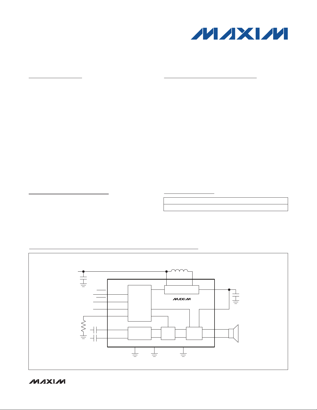
Simplified Block Diagram
BATTERY
LXV
OUTPUT
STAGE
V
CCOUT
A2
A1
PVDD
B1
SPKP
C1
SPKN
SDBST
SDSPK
GAIN
RKNEE B3
INP D2
INN
BAT
B4 A3
D4
C3
B2
D3
CONTROL
DIFFERENTIAL
INPUT
C4 A4 D1, C2
AGND SPKPGNDBSTPGND
BOOST CONVERTER
MAX98500
GAIN
_______________________________________________________________ Maxim Integrated Products 1
For pricing, delivery, and ordering information, please contact Maxim Direct at 1-888-629-4642,
or visit Maxim’s website at www.maxim-ic.com.
Page 2
Boosted 2.2W Class D Amplifier
with Automatic Level Control
ABSOLUTE MAXIMUM RATINGS
V
to AGND .........................................................-0.3V to +6V
BAT
V
to BSTPGND, AGND .................................-0.3V to +6V
CCOUT
PVDD to SPKPGND .................................................-0.3V to +6V
BSTPGND, SPKPGND to AGND ......................... -0.3V to +0.3V
GAIN to AGND ........................................-0.3V to (V
SDBST, SDSPK to AGND ...................................... -0.3V to V
BAT
+ 0.3V)
BAT
All Other Pins (excluding LX) to AGND ..................-0.3V to +6V
Current Into/Out of LX, V
Continuous Current Into/Out of SPK_, PVDD,
MAX98500
, BSTPGND ..................... Q3.9A
CCOUT
SPKPGND .................................................................. Q800mA
Continuous Input Current (all other pins) ........................ Q20mA
Duration of Short Circuit Between V
CCOUT
and BSTPGND ...................................................... Continuous
Note 1: Package thermal resistances were obtained using the method described in JEDEC specification JESD51-7, using a four-
layer board. For detailed information on package thermal considerations, refer to www.maxim-ic.com/thermal-tutorial.
Stresses beyond those listed under “Absolute Maximum Ratings” may cause permanent damage to the device. These are stress ratings only, and functional
operation of the device at these or any other conditions beyond those indicated in the operational sections of the specifications is not implied. Exposure to absolute
maximum rating conditions for extended periods may affect device reliability.
ELECTRICAL CHARACTERISTICS
(V
= 3.6V, RL = J between SPKP and SPKN, AV = +6dB, CIN = 1FF, 20Hz to 22kHz AC measurement bandwidth, TA = T
BAT
T
, unless otherwise noted. Typical values are at TA = +25NC.) (Note 2)
MAX
PARAMETER SYMBOL CONDITIONS MIN TYP MAX UNITS
Power-Supply Rejection Ratio
(Note 3)
Quiescent Current
Combined Efficiency
Shutdown Current I
Turn-On Time t
BOOST CONVERTER
Battery Supply Voltage Range V
Soft-Start Interval t
Undervoltage Lockout UVLO V
Boost Converter Output Voltage V
Output Current Limit I
Input Current Limit I
nMOS Current Limit I
pMOS Turn-Off Current Limit 10 mA
Switching Frequency f
Efficiency
Startup Short-Circuit Time Converter latch off 50 ms
Thermal Shutdown 165
LX Leakage Current
PSRR
I
VBAT
I
PVDD
SHDN
ON
BAT
ON
VCCOUTILOAD
MAX
LIMIT
LX,MAX
T
= +25NC, V
A
TA = +25NC, SDSPK = SDBST = V
T
= +25NC, V
A
TA = +25NC, PVDD = 5.55V, SDSPK =
SDBST = V
E P
OUT
V
SDSPK
Time from power-on to full operation 10 12 ms
BAT
V
BAT
Startup, V
S
E 0.1A P I
= 0V or 5.5V,
V
LX
V
CCOUT
BAT
= 1.7W, f = 1kHz, Z
= V
SDBST
falling 2.1 2.2 2.3 V
= 0mA 5.45 5.5 5.65 V
R = 3.6V
CCOUT
P 0.75A
OUT
= 5.5V
Duration of SPK_ Short Circuit to PVDD or
SPKPGND .............................................................. Continuous
Duration of Short Circuit Between SPKP
and SPKN ..............................................................Continuous
Continuous Power Dissipation, Multilayer Board (T
WLP (derate 20.4mW/NC above +70NC)........................1.33W
θ
(Note 1).................................................................49NC/W
JA
= +70NC)
A
Junction Temperature .....................................................+150NC
Operating Temperature Range .......................... -40NC to +85NC
Storage Temperature Range ............................ -65NC to +150NC
Soldering Temperature (reflow) ......................................+260NC
= 2.5V to 5.5V
BAT
= 0V, SDBST = V
SDSPK
BAT
BAT
95 dB
3.05
0.09 0.15
1.7 2.7
= 8I + 68FH
SPK
= 0V, TA = +25NC
87 %
0.04 1.5
2.5 5.5 V
5.6 ms
1.5 A
= 0V 0.3 0.5 A
3.3 A
1.8 2.0 2.2 MHz
93 %
= +25NC
T
A
-40NC P T
P +85NC
A
-1.0 +0.1 +1.0
0.1
MIN
mA
FA
NC
FA
to
2 ______________________________________________________________________________________
Page 3
Boosted 2.2W Class D Amplifier
with Automatic Level Control
ELECTRICAL CHARACTERISTICS (continued)
(V
= 3.6V, RL = J between SPKP and SPKN, AV = +6dB, CIN = 1FF, 20Hz to 22kHz AC measurement bandwidth, TA = T
BAT
T
, unless otherwise noted. Typical values are at TA = +25NC.) (Note 2)
MAX
PARAMETER SYMBOL CONDITIONS MIN TYP MAX UNITS
SPEAKER AMPLIFIER
Output Offset Voltage V
Click-and-Pop Level K
Output Power (Note 5) P
Total Harmonic Distortion Plus
Noise
Output Switching Frequency 300 kHz
Gain A
Output Current Limit 2 A
Efficiency
Output Noise A-weighted 43
Input Resistance R
Common-Mode Rejection Ratio CMRR f = 1kHz 60 dB
Bias Voltage V
ALC
Attack Time 20
Release Time 1.6 s/dB
Maximum Attenuation 8 dB
Attenuation Resolution 0.5 dB
Knee Voltage V
OUT
THD+N
BIAS
KNEE
TA = +25NC
OS
Peak voltage, TA =
+25NC, A-weighted, 32
samples per second,
CP
Z
= 8I + 68FH,
SPK
(Notes 3, 4)
Z
= 8I + 68FH
SPK
f = 1kHz, P
Z
= 8I + 68FH
SPK
GAIN = AGND 5.5 6 6.5
V
GAIN = V
E P
IN
= 1.7W, f = 1kHz, Z
OUT
SDBST = SDSPK =
V
BAT
V
SDBST
TA = +25NC
= 850mW, TA = +25NC,
OUT
BAT
= V
SDSPK
Into shutdown -56
Out of shutdown -56
THD+N P 1%
THD+N P 10%
= 8I + 68FH
SPK
AV = 6dB
(GAIN = AGND)
= 15.5dB
A
V
(GAIN =
unconnected)
A
= 20dB
V
= 0V
(GAIN = V
All gain settings 110
R
= 154kI
KNEE
= 40.5kI
R
KNEE
R
= 13kI
KNEE
BAT
)
19.5 20 20.5
36 54 72
12 18 26
6.5 11 16
1.3 1.4 1.5 V
2.19 2.3 2.42
3.14 3.3 3.47
3.71 3.9 4.10
1 3 mV
1.7
2.2
0.05 %
92 %
MIN
dBV
W
dBGAIN = unconnected 15 15.5 16
FV
RMS
kI
Fs/dB
V
MAX98500
to
_______________________________________________________________________________________ 3
Page 4
Boosted 2.2W Class D Amplifier
with Automatic Level Control
ELECTRICAL CHARACTERISTICS (continued)
(V
= 3.6V, RL = J between SPKP and SPKN, AV = +6dB, CIN = 1FF, 20Hz to 22kHz AC measurement bandwidth, TA = T
BAT
T
, unless otherwise noted. Typical values are at TA = +25NC.) (Note 2)
MAX
PARAMETER SYMBOL CONDITIONS MIN TYP MAX UNITS
= 3.25V 43.2
V
KNEE
V
= 3.35V 37.4
KNEE
= 3.45V 32.4
V
KNEE
= 3.55V 27.4
V
KNEE
= 3.65V 23.2
V
KNEE
= 3.75V 18.7
V
KNEE
= 3.85V 15.0
V
KNEE
Knee Resistor R
KNEE
MAX98500
DIGITAL INPUTS (SDBST, SDSPK)
Input Voltage High V
Input Voltage Low V
Input Capacitance C
Input Leakage Current I
Note 2: 100% production tested at T
Note 3: Amplifier inputs are AC-coupled to AGND.
Note 4: Mode transitions are controlled by SDSPK.
IN
= +25NC. Specifications over temperature limits are guaranteed by design.
A
iH
IL
IN
TA = +25NC,
A
= 15.5dB
V
TA = +25NC
1.4 V
0.4 V
10 pF
-1.0 +1.0
MIN
kI
FA
to
4 ______________________________________________________________________________________
Page 5
Boosted 2.2W Class D Amplifier
with Automatic Level Control
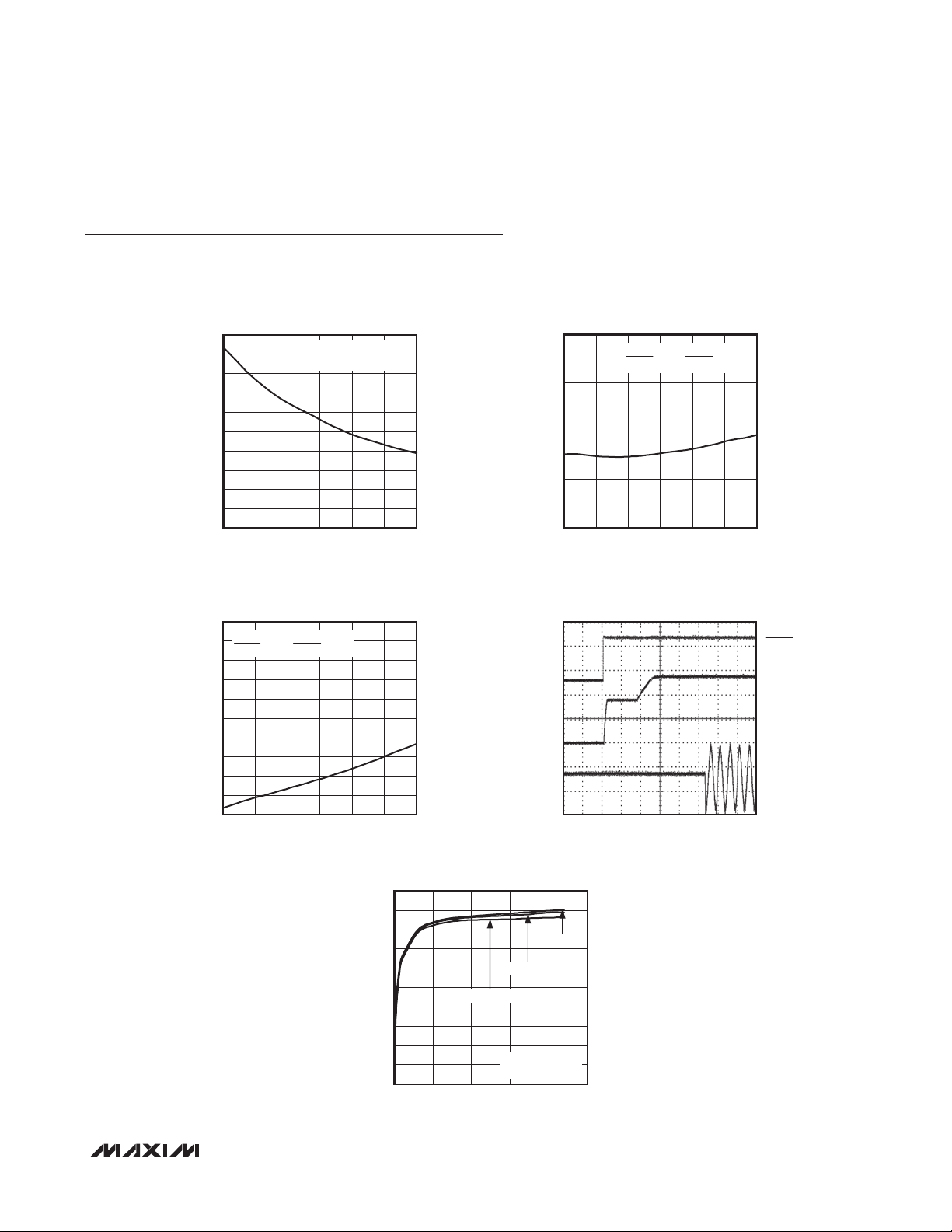
Typical Operating Characteristics
(V
= 3.6V, RL = ∞ between SPKP and SPKN, AV = +15.5dB, RKNEE = V
BAT
otherwise noted.)
General
BATTERY CURRENT
vs. BATTERY VOLTAGE
5.0
4.5
4.0
3.5
3.0
2.5
2.0
1.5
BATTERY CURRENT (mA)
1.0
0.5
0
2.5 5.5
INPUTS AC-COUPLED TO AGND
SDSPK = SDBST = V
BATTERY VOLTAGE (V)
BAT
MAX98500 toc01
5.04.54.03.53.0
, 20Hz to 22kHz AC measurement bandwidth, unless
BAT
BATTERY CURRENT
vs. BATTERY VOLTAGE
140
120
100
BATTERY CURRENT (µA)
80
60
2.5 5.5
INPUTS AC-COUPLED TO AGND
SDSPK = GND, SDBST = V
BATTERY VOLTAGE (V)
BAT
MAX98500 toc02
5.04.54.03.53.0
MAX98500
BATTERY CURRENT
vs. BATTERY VOLTAGE
10
INPUTS AC-COUPLED TO AGND
9
SDSPK = V
8
7
6
5
4
3
BATTERY CURRENT (µA)
2
1
0
2.5 5.5
, SDBST = AGND
BAT
BATTERY VOLTAGE (V)
MAX98500 toc03
5.04.54.03.53.0
EFFICIENCY vs. OUTPUT POWER
100
90
80
70
60
50
40
EFFICIENCY (%)
30
20
10
0
0 2.5
V
BAT
V
= 3.0V
BAT
Z
LOAD
fIN = 1kHz
P
(W)
OUT
OV
OV
OV
V
= 4.2V
BAT
= 3.6V
= 8I + 68µH
2.01.51.00.5
TURN-ON RESPONSE
2ms/div
MAX98500 toc05
MAX98500 toc04
SDBST
2V/div
V
CCOUT
2V/div
SPKR
OUTPUT
1V/div
_______________________________________________________________________________________ 5
Page 6

Boosted 2.2W Class D Amplifier
with Automatic Level Control
Typical Operating Characteristics (continued)
(V
= 3.6V, RL = ∞ between SPKP and SPKN, AV = +15.5dB, RKNEE = V
BAT
otherwise noted.)
Speaker
, 20Hz to 22kHz AC measurement bandwidth, unless
BAT
10
MAX98500
1
0.1
THD+N (%)
0.01
0.001
0.01 100
OUTPUT POWER vs. LOAD RESISTANCE
3.0
2.5
2.0
1.5
1.0
OUTPUT POWER (W)
THD+N vs. FREQUENCY
Z
= 8I + 68µH
LOAD
P
= 1.4W
OUT
FREQUENCY (kHz)
THD+N = 1%
P
= 400mW
OUT
fIN = 1kHz
Z
SPRK
THD+N = 10%
1010.1
= LOAD + 68µF
MAX98500 toc06
MAX98500 toc08
100
Z
= 8I + 68µH
LOAD
10
1
THD+N (%)
0.1
0.01
0.001
0 2.4
f = 6kHz
f = 1kHz
f = 100Hz
OUTPUT POWER (W)
OUTPUT POWER vs. BATTERY VOLTAGE
3.0
fIN = 1kHz
= 8I + 68µH
Z
SPRK
2.5
2.0
THD+N vs. OUTPUT POWER
1.5
1.0
OUTPUT POWER (W)
THD+N = 1%
2.01.61.20.80.4
THD+N = 10%
MAX98500 toc07
MAX98500 toc09
0.5
0
1 1000
LOAD RESISTANCE (I)
10010
0.5
0
2.5 5.5
BATTERY VOLTAGE (V)
5.04.54.03.53.0
GAIN vs. FREQUENCY
30
Z
= 8I + 68µH
LOAD
20
10
0
GAIN (dB)
-10
-20
-30
-40
0.1 1000
AV = 20dB
MAX98500 toc10
AV = 15.5dB
AV = 6dB
100101
FREQUENCY (kHz)
6 ______________________________________________________________________________________
Page 7

Boosted 2.2W Class D Amplifier
with Automatic Level Control
Typical Operating Characteristics (continued)
(V
= 3.6V, RL = ∞ between SPKP and SPKN, AV = +15.5dB, RKNEE = V
BAT
otherwise noted.)
, 20Hz to 22kHz AC measurement bandwidth, unless
BAT
MAX98500
SPEAKER POWER-SUPPLY REJECTION
RATIO vs. FREQUENCY
0
V
AT PVDD = 200mV
RIPPLE
INPUTS AC-COUPLED AGND
-20
-40
PSRR (dB)
-60
-80
-100
0.01 100
FREQUENCY (kHz)
P-P
TURN-ON RESPONSE
SDBST = V
BAT
0V
COMMON-MODE REJECTION RATIO
0
vs. FREQUENCY
Z
= 8I + 68µH
LOAD
MAX98500 toc11
-20
-40
CMRR (dB)
-60
-80
1010.1
-100
0.01 100
MAX98500 toc14
SDSPK
2V/div
AV = 15.5dB
AV = 6dB
AV = 20dB
1010.1
FREQUENCY (kHz)
THD+N = 10%
0V
MAX98500 toc12
0V
0V
CLIPPING RESPONSE
SHUTDOWN RESPONSE
40µs/div
MAX98500 toc15
SPKR
OUTPUT
500mV/div
MAX98500 toc13
SDSPK
2V/div
SPKR
OUTPUT
1V/div
0V
1ms/div
WIDEBAND OUTPUT SPECTRUM
20
0
-20
-40
AMPLITUDE (dBV)
-60
-80
-100
0.1 1000
RBW = 100Hz
AUDIO INPUTS AC-GROUNDED
FREQUENCY (MHz)
100101
SPKR
OUTPUT
1V/div
MAX98500 toc16
200µs/div
INBAND OUTPUT SPECTRUM
0
fIN = 1kHz
OUTPUT = -60dBV
-20
-40
-60
AMPLITUDE (dBV)
-80
-100
-120
0 20
FREQUENCY (kHz)
MAX98500 toc17
15105
_______________________________________________________________________________________ 7
Page 8

Boosted 2.2W Class D Amplifier
with Automatic Level Control
Typical Operating Characteristics (continued)
(V
= 3.6V, RL = ∞ between SPKP and SPKN, AV = +15.5dB, RKNEE = V
BAT
otherwise noted.)
Boost Converter
, 20Hz to 22kHz AC measurement bandwidth, unless
BAT
100
98
MAX98500
96
94
92
90
88
EFFICIENCY (%)
86
84
82
80
0 1600
OUTPUT VOLTAGE vs. OUTPUT CURRENT
5.52
5.51
5.50
5.49
5.48
5.47
OUTPUT VOLTAGE (V)
5.46
5.45
5.44
0 1600
EFFICIENCY vs. OUTPUT CURRENT
V
= 4.2V
BAT
V
= 4V
BAT
V
= 3.6V
BAT
V
= 3V
BAT
I
OUT
V
BAT
V
= 3V
BAT
V
= 3.3V
BAT
V
= 3.6V
BAT
I
OUT
(mA)
= 4.2V
(A)
V
= 5V
BAT
V
= 3.3V
BAT
14001200800 1000400 600200
V
= 5V
BAT
14001200200 400 600 800 1000
MAX98500 toc18
MAX98500 toc20
LOAD REGULATION vs. OUTPUT CURRENT
0.2
0
V
= 5V
BAT
-0.2
-0.4
-0.6
LOAD REGULATION (%)
-0.8
V
-1.0
-1.2
0 1600
BAT
= 3.6V
V
= 4.2V
BAT
V
= 4V
BAT
V
= 3.3V
BAT
V
= 3V
BAT
I
(mA)
OUT
SWITCHING FREQUENCY
vs. BATTERY VOLTAGE
2.04
2.02
I
= 100mA
OUT
2.00
I
= 500mA
1.98
SWITCHING FREQUENCY (MHz)
1.96
OUT
2.5 4.5
BATTERY VOLTAGE (V)
MAX98500 toc19
140012001000800600400200
MAX98500 toc21
4.34.13.93.73.53.33.12.92.7
SOFT-START
1ms/div
MAX98500 toc22
SDBST
2V/div
0V
V
CCOUT
2V/div
0V
8 ______________________________________________________________________________________
Page 9
Boosted 2.2W Class D Amplifier
with Automatic Level Control
Pin Configuration
TOP VIEW
(BUMP SIDE DOWN)
MAX98500
V
2 3 41
CCOUT
LX BSTPGNDPVDD
+
A
MAX98500
B
SPKP
C
D
GAIN RKNEE V
SPKPGND
SDSPK
INP INNSPKPGND
WLP
BAT
AGNDSPKN
SDBST
Pin Description
BUMP NAME FUNCTION
A1 PVDD
A2 V
CCOUT
A3 LX Boost Switch Input
A4 BSTPGND Boost Power Ground
B1 SPKP Positive Speaker Output
B2 GAIN
B3 RKNEE ALC Knee Voltage Set Input. Set the ALC knee voltage with a resistor to AGND.
B4 V
BAT
C1 SPKN Negative Speaker Output
C2, D1 SPKPGND Speaker Ground
C3
SDSPK Speaker Output Shutdown. Drive SDSPK low to shutdown the speaker output.
C4 AGND Analog Ground
D2 INP Positive Audio Input
D3 INN Negative Audio Input
D4 SDBST
Speaker Amplifier Power Supply. Bypass to SPKPGND with a 0.1mF capacitor.
Boost Converter Output. Connect a 22mF (0805) capacitor between V
CCOUT
and
BSTPGND.
Gain Select Input. Connect GAIN to ground to set the speaker gain to 6dB. Leave GAIN
unconnected to set the speaker gain to 15.5dB. Connect GAIN to V
to set the speaker
BAT
gain to 20dB.
Battery Voltage Input. Connect a 10mF (0805) capacitor between V
and BSTPGND.
BAT
Include at least 22mF of system bulk capacitance.
Boost Converter Shutdown. Drive SDBST low to shutdown the boost converter and the
speaker output.
_______________________________________________________________________________________ 9
Page 10
Boosted 2.2W Class D Amplifier
with Automatic Level Control
Detailed Description
The MAX98500 is a high-efficiency Class D audio amplifier that features an integrated boost converter to deliver a
constant output power over a large range of battery supply
voltages. The boost converter operates at 2MHz, requiring
only a small (2.2FH) external inductor and output capacitor. The amplifier has differential inputs and an internal fully
differential design with three gain settings (6dB, 15.5dB,
and 20dB) that are selectable with a logic input.
MAX98500
The MAX98500 also features automatic level control. The
automatic level control reduces the output swing when
the battery voltage decreases to prevent the collapse of
battery voltage.
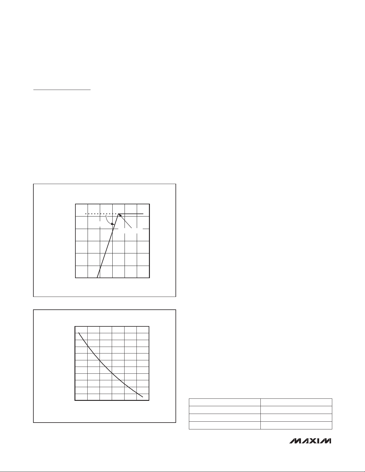
PEAK AMPLIFIER OUTPUT VOLTAGE
vs. BATTERY VOLTAGE
6
)
PEAK
5
4
3
2
1
PEAK AMPLIFIER OUTPUT VOLTAGE (V
0
Figure 1. Typical Tracking Function
4.0
3.9
3.8
3.7
3.6
(V)
3.5
KNEE
3.4
V
3.3
3.2
3.1
3.0
2.9
Figure 2. The Relationship of R
SLOPE
KNEE VOLTAGE
06
BATTERY VOLTAGE (V)
V
vs. R
KNEE
10 70
R
(kI)
KNEE
and V
KNEE
52341
KNEE
6050403020
KNEE
Class D Speaker Amplifier
The MAX98500 filterless Class D amplifier offers much
higher efficiency than Class AB amplifiers. The high
efficiency of a Class D amplifier is due to the switching
operation of the output stage transistors. Any power loss
associated with the Class D output stage is mostly due to
2
the I
R loss of the MOSFET on-resistance and quiescent
current overhead.
Low-EMI Filterless Output Stage
Traditional Class D amplifiers require the use of external
LC filters, or shielding, to meet EN55022B electromagnetic-interference (EMI) regulation standards. Maxim’s
active emissions limiting edge-rate control circuitry
reduces EMI emissions, while maintaining up to 92%
efficiency (speaker only). Above 10MHz, the wideband
spectrum looks like noise for EMI purposes.
Automatic Level Control
The MAX98500 features an automatic level control circuit
that limits the maximum speaker output swing. This helps:
U Avoid clipping
U Save the battery from collapsing, which could cause
a reset of the system
The limiter keeps the peak voltage below a value that is a
function of battery voltage, as shown in Figure 1.
The full output swing of 5.2V is maintained for battery
voltages down to the knee voltage, while for lower battery
voltages the maximum V
-swing is reduced by 3V/V.
PEAK
The knee voltage can be changed by applying different
resistors between RKNEE and AGND. The typical tracking function is shifted horizontally with different R
KNEE
resistor values (Figure 2).
The preamplifier gain reduces as the automatic level
control activates. The maximum gain reduction is 8dB
with a resolution of 0.5dB steps.
The attack (gain reduction) happens immediately (20Fs/
dB), while the release is set to 1.6s/dB.
GAIN Select
The MAX98500 features three internal gain settings that
are selectable with the GAIN input. Table 1 shows the
gain settings.
Table 1. Gain Settings
GAIN AMPLIFIER GAIN (dB)
AGND 6
Unconnected 15.5
V
BAT
20
10 _____________________________________________________________________________________
Page 11

Boosted 2.2W Class D Amplifier
with Automatic Level Control
Table 2. Shutdown Configurations
SDBST SDSPK
Low Low Off Off
Low High Off Off
High Low On Off
High High On On
The MAX98500 features two active-low shutdown inputs
(SDSPK and SDBST). Table 2 shows the different shutdown configurations.
BOOST
STATUS
Click-and-Pop Suppression
The MAX98500 speaker amplifier features Maxim’s comprehensive click-and-pop suppression. During startup,
the click-and-pop suppression circuitry reduces any
audible transient sources internal to the device. When
entering shutdown, the differential speaker outputs ramp
down to SPKPGND quickly and simultaneously.
Current-Limit and Thermal Protection
The IC features overcurrent and thermal protection.
The IC shuts down when the V
to about 80% of the expected output. The IC also
enters into shutdown when the die temperature exceeds
+165NC. The device remains in shutdown until power
is reset or SDBST is toggled low and back high after
the fault condition has been removed. The IC speaker
amplifier also features a 2A (typ) short-circuit protection
scheme.
CCOUT
Boost Converter
The MAX98500 features a two-stage, soft-start, powerup sequence. When SDBST is taken high and V
above UVLO the soft-start first ramps V
to V
Once the V
switching turns on and ramps the V
(typ), see the Soft-Start graph in the Typical Operating
Characteristics. The maximum load current is available
after the soft-start is completed.
The undervoltage lockout (UVLO) circuit compares the
voltage at V
ensure that the input voltage is high enough for reliable
operation. Once the V
voltage with a battery current of 300mA (typ).
BAT
CCOUT
reaches the V
Undervoltage Lockout (UVLO)
with the UVLO threshold (2.2V typ) to
BAT
voltage exceeds the UVLO
BAT
voltage, the internal
BAT
CCOUT
SPEAKER
STATUS
Shutdown
output decreases
Soft-Start
is
BAT
quickly
CCOUT
to 5.5V in 5ms
threshold, the soft-start begins. When the input voltage
falls below the UVLO threshold, the boost converter and
speaker amplifier turn off.
Applications Information
Filterless Class D Operation
Traditional Class D amplifiers require an output filter to
recover the audio signal from the amplifier’s output. The
filter adds cost, increases the solution size of the amplifier, and can decrease efficiency and THD+N performance. The traditional PWM scheme uses large differential output swings (2 x supply voltage peak-to-peak) and
causes large ripple currents. Any parasitic resistance in
the filter components results in a loss of power and lowers the efficiency.
The MAX98500 does not require an output filter. The
device relies on the inherent inductance of the speaker
coil and the natural filtering of both the speaker and
the human ear to recover the audio component of the
square-wave output. Eliminating the output filter results
in a smaller, less costly, and more efficient solution.
Because the frequency of the MAX98500 output is well
beyond the bandwidth of most speakers, voice coil
movement due to the square-wave frequency is very
small. Although this movement is small, a speaker not
designed to handle the additional power can be damaged. For optimum results, use a speaker with a series
inductance > 10FH. Typical 8I speakers exhibit series
inductances in the 20FH to 100FH range.
RF Susceptibility
GSM radios transmit using time-division multiple access
(TDMA) with 217Hz intervals. The result is an RF signal
with strong amplitude modulation at 217Hz and its harmonics that is easily demodulated by audio amplifiers.
The MAX98500 is designed specifically to reject RF
signals; however, PCB layout has a large impact on the
susceptibility of the end product.
In RF applications, improvements to both layout and
component selection decrease the MAX98500’s susceptibility to RF noise and prevent RF signals from being
demodulated into audible noise. Trace lengths should be
kept below 1/4 of the wavelength of the RF frequency of
interest. Minimizing the trace lengths prevents them from
functioning as antennas and coupling RF signals into the
MAX98500. The wavelength (l) in meters is given by:
l = c/f where c = 3 x 10
of interest.
8
m/s, and f = the RF frequency
MAX98500
______________________________________________________________________________________ 11
Page 12
Boosted 2.2W Class D Amplifier
with Automatic Level Control
Route audio signals on the middle layers of the PCB to
allow the ground planes above and below to shield them
from RF interference. Ideally the top and bottom layers
of the PCB should primarily be ground planes to create
effective shielding.
Additional RF immunity can also be obtained from relying on the self-resonant frequency of capacitors as it
exhibits the frequency response similar to a notch filter.
Depending on the manufacturer, 10pF to 20pF capacitors
MAX98500
typically exhibit self resonance at RF frequencies. These
capacitors, when placed at the input pins, can effectively
shunt the RF noise at the inputs of the MAX98500. For
these capacitors to be effective, they must have a lowimpedance, low-inductance path to the ground plane.
Do not use microvias to connect to the ground plane as
these vias do not conduct well at RF frequencies.
Speaker Component Selection
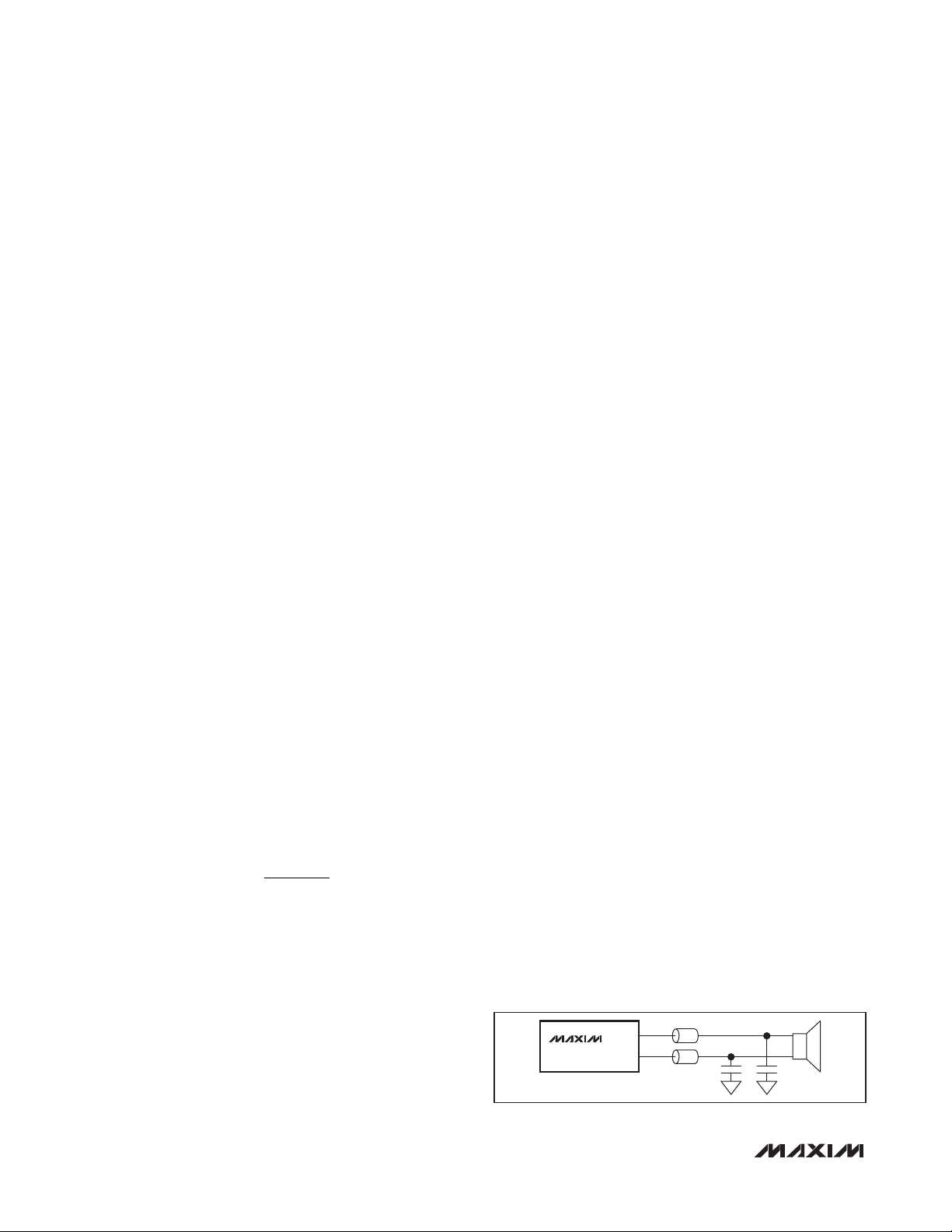
Optional Ferrite Bead Filter
Additional EMI suppression can be achieved using a
filter constructed from a ferrite bead and a capacitor to
ground (Figure 3). Use a ferrite bead with low DC resistance, high-frequency (> 100MHz) impedance between
100I and 600I, and rated for at least 1A. The capacitor
value varies based on the ferrite bead chosen and the
actual speaker lead length. Select a capacitor less than
1nF based on EMI performance.
Input Capacitor (C
An input capacitor, C
impedance of the MAX98500 speaker inputs forms a
highpass filter that removes the DC bias from an incoming analog signal. The AC-coupling capacitor allows the
amplifier to automatically bias the signal to an optimum
DC level. Assuming zero-source impedance, the -3dB
point of the highpass filter is given by:
Choose C
quency of interest. For best audio quality, use capacitors
whose dielectrics have low-voltage coefficients, such as
tantalum or aluminum electrolytic. Capacitors with highvoltage coefficients, such as ceramics, could result in
increased distortion at low frequencies.
such that f
IN
, in conjunction with the input
IN
f
-3dB
-3dB
1
=
2 R C
π
IN IN
is well below the lowest fre-
IN
Boost Converter Component Selection
Inductor Selection
In most step-up converter designs, a reasonable inductor value can be derived from the following equation.
This equation sets peak-to-peak inductor current at 1/2
the DC inductor current:
L = (2 x V
where f
factor given by D = 1 - (V
equation above results in a peak-to-peak inductor current ripple of 0.5 x I
current of 1.25 x I
tion) current rating of the inductor meets or exceeds this
requirement.
The recommended nominal inductance for the MAX98500
is 2.2FH. Nominal inductance decreases as the inductor
current increases. If the decrease from the nominal
inductance is severe, the boost converter may become
unstable or shut down at lower output power levels than
expected. Ensure the minimum inductance at the peak
inductor current is 1.0FH.
An output capacitor, C
output voltage ripple small and to ensure regulation loop
stability. The output capacitor must have low impedance at the switching frequency. Ceramic capacitors
)
are highly recommended due to their small size and low
ESR. Ceramic capacitors with X5R or X7R temperature
characteristics generally perform well. The recommended nominal capacitance for the MAX98500 is 22FF (0805
case size or larger). Ensure the minimum capacitance at
5.5V is 6.8FF.
An input capacitor, C
drawn from the battery or input power source and reduces switching noise in the IC. The impedance of the input
capacitor at the switching frequency should be kept very
low. Ceramic capacitors are highly recommended due
to their small size and low ESR. Ceramic capacitors with
X5R or X7R temperature characteristics generally perform well. One 10FF ceramic capacitor is recommended
with a system bulk capacitance of 22FF or larger.
is the switching frequency, and D is the duty
SW
MAX98500
x D x (1-D))/(I
BATT
OUT
/(1 - D). Ensure the peak (satura-
OUT
VBAT
SPKP
SPKN
OUT(MAX
BAT/VOUT
/(1 - D), and a peak inductor
Output Capacitor (C
VCCOUT
, reduces the current peaks
). Using L from the
, is required to keep the
Input Capacitor (C
)
x fSW)
VCCOUT
VBAT
)
)
Figure 3. Optional Class D Ferrite Bead Filter
12 _____________________________________________________________________________________
Page 13

Boosted 2.2W Class D Amplifier
with Automatic Level Control
Supply Bypassing, Layout, and Grounding
Proper layout and grounding are essential for optimum
performance. Use a large continuous ground plane on
a dedicated layer of the PCB to minimize loop areas.
Connect AGND and BSTPGND/SPKPGND directly to the
ground plane using the shortest traces length possible.
Proper grounding improves audio performance, and
prevents any digital noise from coupling into the analog
audio signals.
0.25mm
0.22mm
Figure 4. Recommended PCB Footprint
Bypass V
with a 10FF capacitor and a system
BAT
bulk capacitance of 22FF or larger. Bypass PVDD to
SPKPGND with a 0.1FF capacitor and with as minimal a
loop area as possible. Connect SPKP and SPKN to the
speaker using the shortest and widest traces possible.
Reducing trace length minimizes radiated EMI. Route
SPKP/SPKN as a differential pair on the PCB to minimize
loop area, thereby, the inductance of the circuit. If filter
components are used on the speaker outputs, be sure
to locate them as close as possible to the MAX98500 to
ensure maximum effectiveness. Minimize the trace length
from any ground-tied passive components to SPKPGND
to further minimize radiated EMI.
An evaluation kit (MAX98500 Evaluation Kit) is available
to provide an example layout for the MAX98500.
WLP Applications Information
For the latest application details on WLP construction,
dimensions, tape carrier information, PCB techniques,
bump-pad layout, and recommended reflow temperature profile, as well as the latest information on reliability
testing results, refer to the Application Note 1891: Wafer-
Level Packaging (WLP) and Its Applications on Maxim’s
website at www.maxim-ic.com/ucsp. See Figure 4 for the
recommended PCB footprint for the MAX98500.
MAX98500
Typical Application Circuit
2.2µH
BATTERY
C
VBAT
C
1µF
C
1µF
IN
IN
10µF
0805
10%
SDBST
SDSPK
GAIN
RKNEE B3
INP D2
INN
D4
C3
B2
D3
CONTROL
DIFFERENTIAL
INPUT
C4 A4 D1, C2
AGND SPKPGNDBSTPGND
GAIN
22µF*
27.4kI
1%
*SYSTEM LEVEL REQUIREMENT
______________________________________________________________________________________ 13
20%
V
BAT
B4 A3
BOOST CONVERTER
MAX98500
OUTPUT
STAGE
LX
V
CCOUT
A2
A1
PVDD
B1
SPKP
C1
SPKN
0.1µF
10%
8I
C
VCCOUT
22µF
0805
10%
Page 14

Boosted 2.2W Class D Amplifier
with Automatic Level Control
Package Information
For the latest package outline information and land patterns, go to www.maxim-ic.com/packages. Note that a “+”, “#”, or “-” in the
package code indicates RoHS status only. Package drawings may show a different suffix character, but the drawing pertains to the
package regardless of RoHS status.
PACKAGE TYPE PACKAGE CODE DOCUMENT NO.
16 WLP W162B2+1
21-0200
MAX98500
14 _____________________________________________________________________________________
Page 15

Boosted 2.2W Class D Amplifier
with Automatic Level Control
Revision History
MAX98500
REVISION
NUMBER
0 5/10 Initial release —
REVISION
DATE
DESCRIPTION
PAGES
CHANGED
Maxim cannot assume responsibility for use of any circuitry other than circuitry entirely embodied in a Maxim product. No circuit patent licenses are implied.
Maxim reserves the right to change the circuitry and specifications without notice at any time.
Maxim Integrated Products, 120 San Gabriel Drive, Sunnyvale, CA 94086 408-737-7600 15
©
2010 Maxim Integrated Products Maxim is a registered trademark of Maxim Integrated Products, Inc.
 Loading...