

Page 1
General Description
The MAX9820 Windows Vista®-compliant stereo headphone amplifier is designed for portable equipment
where board space is at a premium. It features Maxim’s
patented DirectDrive
®
architecture to produce a
ground-referenced output from a single supply, eliminating the large output-coupling capacitors required by
conventional single-supply headphone amplifiers.
The MAX9820 features an undervoltage lockout that
prevents over discharging of the battery during
brownout conditions, click-and-pop suppression that
eliminates audible transients on startup, a low-power
shutdown mode, and thermal-overload and short-circuit
protection. Additionally, the MAX9820 suppresses RF
radiation received by input and supply traces acting as
antennas and prevents the amplifier from demodulating
the coupled noise.
The MAX9820 is available in a 10-pin TDFN package
(3mm x 3mm x 0.8mm) and specified over the -40°C to
+85°C extended temperature range.
Applications
Cell Phones
MP3 Players
Notebook PCs
PDAs
Features
o Clickless/Popless Operation
o High RF Noise Rejection
o Windows Vista Premium Mobile Compliant
o 2.7V to 5.5V Single-Supply Operation
o 95mW Output Power (32Ω, V
DD
= 5V)
o Low-Current Shutdown Mode, < 1µA
o Low 3mA (V
DD
= 3.3V) Quiescent Current
o Space-Saving, 3mm x 3mm, 10-Pin TDFN Package
MAX9820
DirectDrive Headphone Amplifier
with External Gain
________________________________________________________________
Maxim Integrated Products
1
19-4666; Rev 0; 7/09
For pricing, delivery, and ordering information, please contact Maxim Direct at 1-888-629-4642,
or visit Maxim’s website at www.maxim-ic.com.
EVALUATION KIT
AVAILABLE
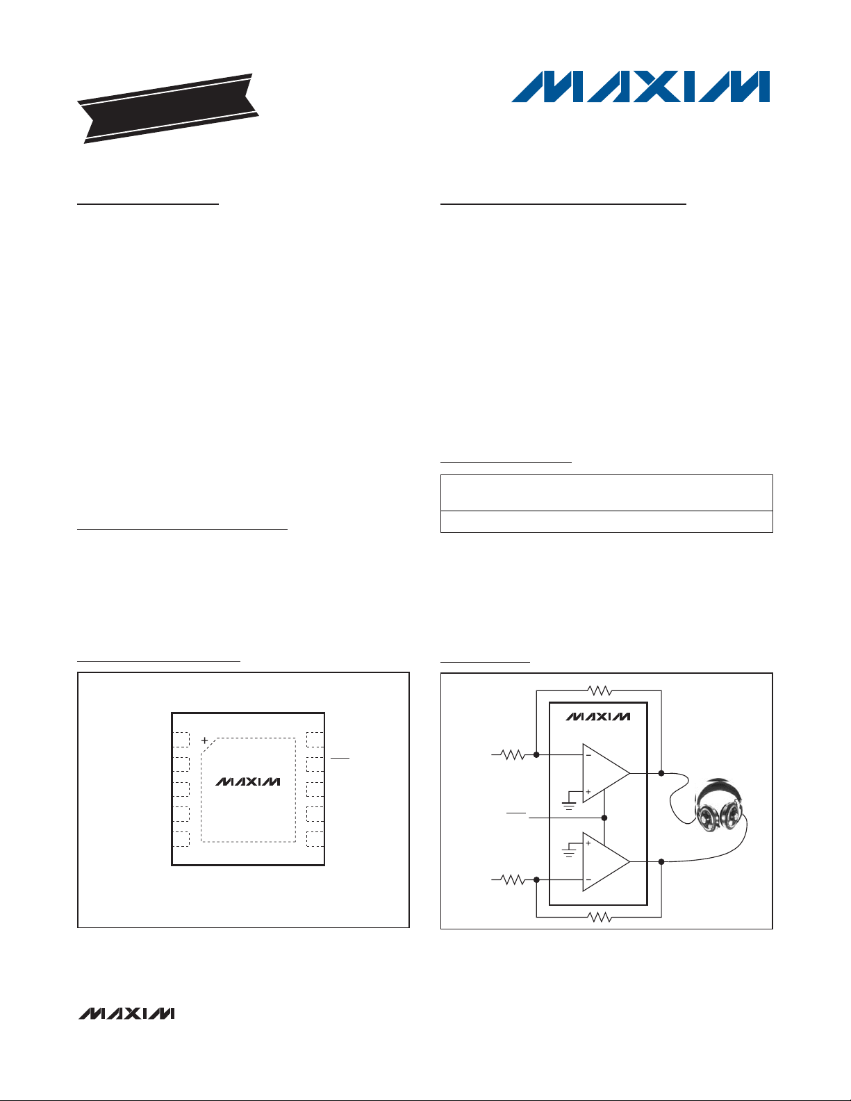
Pin Configuration
Ordering Information
+
Denotes a lead(Pb)-free/RoHS-compliant package.
*
EP = Exposed pad.
Simplified Block Diagram
Windows Vista is a registered trademark of Microsoft Corp.
DirectDrive is a registered trademark of Maxim Integrated Products, Inc.
PART TEMP RANGE
MAX9820ETB+ -40°C to +85°C 10 TDFN-EP* AUU
PIN-
PACKAGE
TOP MARK
TOP VIEW
C1P
1
C1N
29
V
3
SS
OUTL
4
56
*EXPOSED PAD.
MAX9820
*EP
TDFN
GND
10
SHDN
V
8
DD
INL
7
INROUTR
LEFT
AUDIO
INPUT
RIGHT
AUDIO
INPUT
MAX9820
SHDN
DirectDrive OUTPUTS
ELIMINATE DC-BLOCKING
CAPACITORS
Page 2
MAX9820
DirectDrive Headphone Amplifier
with External Gain
2 _______________________________________________________________________________________
ABSOLUTE MAXIMUM RATINGS
ELECTRICAL CHARACTERISTICS
(VDD= V
SHDN
= 5V, V
GND
= 0V, RIN= RFB= 40.2kΩ (gain = -1V/V), C1 = C2 = 1µF, C3 = 10µF, R
LOAD
= ∞, TA= -40°C to +85°C,
unless otherwise noted. Typical values are at T
A
= +25°C, unless otherwise noted.) (Note 2)
Stresses beyond those listed under “Absolute Maximum Ratings” may cause permanent damage to the device. These are stress ratings only, and functional
operation of the device at these or any other conditions beyond those indicated in the operational sections of the specifications is not implied. Exposure to
absolute maximum rating conditions for extended periods may affect device reliability.
VDDto GND..............................................................-0.3V to +6V
C1P to GND................................................-0.3V to (V
DD
+ 0.3V)
C1N to GND ................................................(V
SS
- 0.3V) to +0.3V
V
SS
to GND...............................................................-6V to +0.3V
OUTR, OUTL to GND.............................................................±3V
SHDN to GND...........................................................-0.3V to +6V
INR, INL to GND.........................................-0.3V to (V
DD
+ 0.3V)
OUTR, OUTL Short Circuit to GND, V
DD
....................Continuous
Short Circuit Between OUTL and OUTR ....................Continuous
Continuous Input Current (Into All Other Pins) .................±20mA
Continuous Power Dissipation (T
A
= +70°C)
10-Pin TDFN Single-Layer PCB (derate 18.5mW/°C
above +70°C)........................................................1481.5mW
Junction-to-Case Thermal Resistance (θ
JC
) (Note 1)
10-Pin TDFN ................................................................8.5°C/W
Junction-to-Ambient Thermal Resistance (θ
JA
) (Note 1)
10-Pin TDFN...............................................................41.0°C/W
Continuous Power Dissipation (T
A
= +70°C)
10-Pin TDFN Multilayer PCB (derate 24.4mW/°C
above +70°C)...........................................................1951mW
Junction-to-Case Thermal Resistance (θ
JC
) (Note 1)
10-Pin TDFN.................................................................9.0°C/W
Junction-to-Ambient Thermal Resistance (θ
JA
) (Note 1)
10-Pin TDFN...............................................................41.0°C/W
Operating Temperature Range ...........................-40°C to +85°C
Storage Temperature Range .............................-65°C to +150°C
Junction Temperature......................................................+150°C
Lead Temperature (soldering, 10s) .................................+300°C
Note 1: Package thermal resistances were obtained using the method described in JEDEC specification JESD51-7, using a four-
layer board. For detailed information on package thermal considerations, refer to www.maxim-ic.com/thermal-tutorial
.
GENERAL
Supply Voltage Range V
Undervoltage Lockout UVLO 2.2 V
Quiescent Current I
Shutdown Current I
Output Signal Attenuation in
Shutdown
Output Impedance in
Shutdown
Turn-On Time t
Output Offset Voltage V
Click-and-Pop Level K
PARAMETER SYMBOL CONDITIONS MIN TYP MAX UNITS
DD
DD
SHDNVSHDN
ON
OS
CP
Guaranteed by PSRR test 2.7 5.5 V
VDD = 3.3V 3.0 4.6
VDD = 5V 4.0 6.0
= 0V, TA = +25°C < 0.1 1 µA
V
= 0V, VIN = 1V
SHDN
V
= 0V 0.6 kΩ
SHDN
TA = +25°C (Note 3) ±0.1 ±0.5 mV
Z
= 32Ω + 1µH, peak
LOAD
voltage, A-weighted, 32 samples
per second (Notes 3, 4)
Z
= 10kΩ, peak voltage,
LOAD
A-weighted, 32 samples per
second (Notes 3, 4)
RMS
, R
= 10kΩ -110 dBV
LOAD
Into shutdown -79
Out of
shutdown
Into shutdown -62
Out of
shutdown
0.56 ms
-77
-58
mA
dBV
Page 3
MAX9820
DirectDrive Headphone Amplifier
with External Gain
_______________________________________________________________________________________ 3
ELECTRICAL CHARACTERISTICS (continued)
(VDD= V
SHDN
= 5V, V
GND
= 0V, RIN= RFB= 40.2kΩ (gain = -1V/V), C1 = C2 = 1µF, C3 = 10µF, R
LOAD
= ∞, TA= -40°C to +85°C,
unless otherwise noted. Typical values are at T
A
= +25°C, unless otherwise noted.) (Note 2)
Note 2: All specifications are 100% tested at T
A
= +25°C; temperature limits are guaranteed by design.
Note 3: The amplifier inputs are AC-coupled to GND.
Note 4: Mode transitions are controlled by SHDN.
Power-Supply Rejection Ratio PSRR
Output Power P
Total Harmonic Distortion
Plus Noise
Signal-to-Noise Ratio SNR Z
Output Noise V
Crosstalk
Capacitive Load Drive C
Oscillator Frequency f
Thermal Shutdown 145 °C
Thermal Shutdown Hysteresis 15 °C
DIGITAL INPUT (SHDN)
Input Voltage High V
Input Voltage Low V
Input Leakage Current I
PARAMETER SYMBOL CONDITIONS MIN TYP MAX UNITS
OUT
THD+N
NOISE
L
OSC
INH
INL
LEAKAGE TA
V
= 2.7V to 5.5V, TA = +25°C (Note 3) 75 90
DD
f = 1kHz, 200mV
f = 20kHz, 200mV
Z
= 32Ω + 1µH, f = 1kHz,
LOAD
THD+N = 1%
Z
= 16Ω + 1µH, f = 1kHz,
LOAD
THD+N = 1%
Z
= 16Ω + 1µH, f = 1kHz, P
LOAD
Z
= 32Ω + 1µH, f = 1kHz, P
LOAD
Z
= 10kΩ, f = 1kHz, V
LOAD
= 32Ω + 1µH, P
LOAD
(Note 3) 73
P-P
(Note 3) 55
P-P
VDD = 3.6V 45
= 5.0V 95
V
DD
VDD = 3.6V 32
= 5.0V 75
V
DD
= 20mW 0.014
OUT
= 20mW 0.005
OUT
= 1V
OUT
= 25mW, A-weighted 105 dB
OUT
RMS
A-weighted (Note 3) 9 µV
Z
= 32Ω + 1µH
LOAD
L to R, R to L,
BW = 20Hz to 15kHz
FS = 0.300V
V
OUT
Z
LOAD
FS = 0.707V
V
OUT
RMS
= 30mV
= 10kΩ
RMS
= 70.7mV
RMS
No sustained oscillations 200 pF
TA = +25°C 300 500 800 kHz
= +25°C ±1 µA
,
,
RMS
0.001
73
73
1.2 V
0.3 V
dB
mW
%
dB
Page 4
MAX9820
DirectDrive Headphone Amplifier
with External Gain
4 _______________________________________________________________________________________
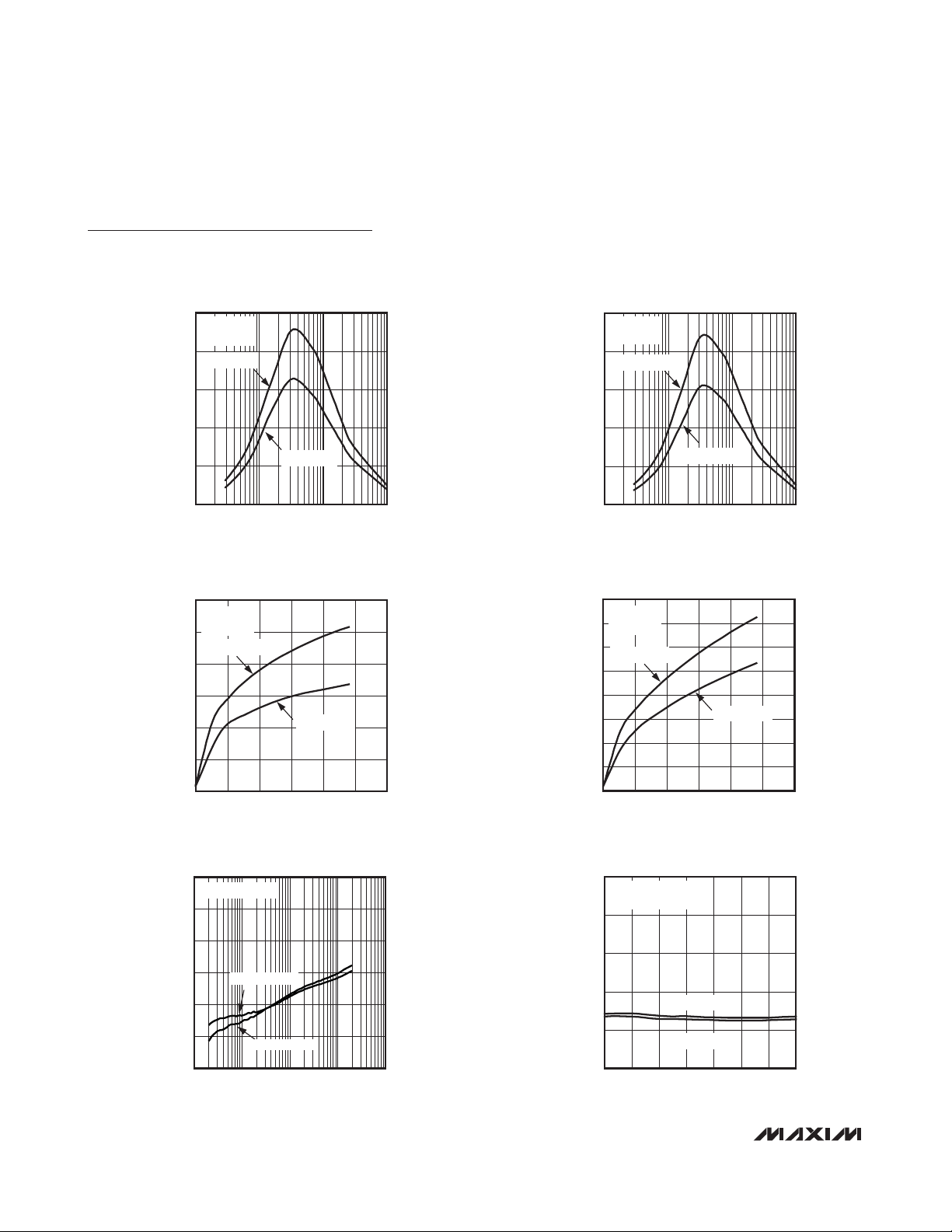
Typical Operating Characteristics
(VDD= V
SHDN
= 5V, V
GND
= 0V, RIN= RFB= 40.2kΩ (gain = -1V/V), C1 = C2 = 1µF, C3 = 10µF, R
LOAD
= ∞. Typical values are at T
A
= +25°C, unless otherwise noted.)
10
1
THD+N vs. OUTPUT POWER
V
= 5.0V
DD
I
R
L
LOAD
LOAD
= 16
= 1FH
MAX9820 toc01
0.1
THD+N (%)
f = 100Hz
f = 6kHz
10
1
0.1
THD+N (%)
THD+N vs. OUTPUT POWER
V
= 5.0V
DD
I
R
= 32
LOAD
L
= 1FH
LOAD
f = 100Hz
MAX9820 toc02
f = 6kHz
0.01
0.001
0 0.14
OUTPUT POWER (W)
f = 1kHz
THD+N vs. OUTPUT POWER
10
V
= 3.6V
DD
I
R
= 16
LOAD
= 1FH
L
LOAD
1
f = 100Hz
0.1
THD+N (%)
0.01
0.001
OUTPUT POWER (W)
f = 1kHz
THD+N vs. FREQUENCY
10
V
= 5.0V
DD
I
R
= 16
LOAD
L
= 1FH
LOAD
1
0.120.100.080.060.040.02
f = 6kHz
0.050.040.030.020.010 0.06
MAX9820 toc03
MAX9820 toc05
0.01
0.001
0 0.16
OUTPUT POWER (W)
f = 1kHz
THD+N vs. OUTPUT POWER
10
V
= 3.6V
DD
I
R
= 32
LOAD
= 1FH
L
LOAD
1
0.1
THD+N (%)
0.01
0.001
f = 100Hz
f = 1kHz
OUTPUT POWER (W)
THD+N vs. FREQUENCY
10
V
= 5.0V
DD
I
R
= 32
LOAD
L
= 1FH
LOAD
1
0.140.120.100.080.060.040.02
MAX9820 toc04
f = 6kHz
0.070.060.050.040.030.020.010 0.08
MAX9820 toc06
0.1
THD+N (%)
0.01
0.001
P
= 20mW
OUT
FREQUENCY (Hz)
P
= 60mW
OUT
10,000100010010 100,000
0.1
THD+N (%)
0.01
0.001
P
OUT
= 20mW
FREQUENCY (Hz)
P
= 60mW
OUT
10,000100010010 100,000
Page 5

MAX9820
DirectDrive Headphone Amplifier
with External Gain
_______________________________________________________________________________________ 5
Typical Operating Characteristics
(VDD= V
SHDN
= 5V, V
GND
= 0V, RIN= RFB= 40.2kΩ (gain = -1V/V), C1 = C2 = 1µF, C3 = 10µF, R
LOAD
= ∞. Typical values are at T
A
= +25°C, unless otherwise noted.)
THD+N vs. FREQUENCY
10
V
= 3.6V
DD
I
R
= 16
LOAD
= 1FH
L
LOAD
1
0.1
THD+N (%)
0.01
0.001
P
OUT
= 10mW
P
FREQUENCY (Hz)
VISTA THD+N vs. FREQUENCY
0
V
= 5.0V
DD
I
R
= 32
LOAD
-20
L
= 1FH
LOAD
V
= -3dBFS
OUT
-40
OUT
= 20mW
10,000100010010 100,000
MAX9820 toc07
MAX9820 toc09
10
1
0.1
THD+N (%)
0.01
0.001
0
-20
-40
THD+N vs. FREQUENCY
V
= 3.6V
DD
I
R
= 32
LOAD
= 1FH
L
LOAD
P
= 30mW
OUT
P
= 10mW
OUT
10,000100010010 100,000
FREQUENCY (Hz)
VISTA THD+N vs. FREQUENCY
V
= 5.0V
DD
I
R
= 10k
LOAD
L
= 1µH
LOAD
V
= -3dBFS
OUT
MAX9820 toc08
MAX9820 toc10
-60
THD+N (dBFS)
-80
-100
-120
FS = 1V
RMS
10 100,000
FREQUENCY (Hz)
FS = 300mV
10,0001000100
OUTPUT POWER vs. SUPPLY VOLTAGE
180
150
120
(mW)
90
OUT
P
60
30
0
2.7 5.5
R
L
LOAD
LOAD
= 16
= 1µH
I
THD+N = 10%
THD+N = 1%
SUPPLY VOLTAGE (V)
RMS
-60
THD+N (dBFS)
-80
-100
-120
10 100,000
FS = 707mV
FS = 1V
10,0001000100
FREQUENCY (Hz)
RMS
RMS
OUTPUT POWER vs. SUPPLY VOLTAGE
180
MAX9820 toc11
5.14.74.33.93.53.1
150
120
(mW)
90
OUT
P
60
30
0
2.7 5.5
R
L
LOAD
LOAD
= 32
= 1µH
THD+N = 10%
I
MAX9820 toc12
THD+N = 1%
5.14.74.33.93.53.1
SUPPLY VOLTAGE (V)
Page 6
MAX9820
DirectDrive Headphone Amplifier
with External Gain
6 _______________________________________________________________________________________
Typical Operating Characteristics (continued)
(VDD= V
SHDN
= 5V, V
GND
= 0V, RIN= RFB= 40.2kΩ (gain = -1V/V), C1 = C2 = 1µF, C3 = 10µF, R
LOAD
= ∞. Typical values are at T
A
= +25°C, unless otherwise noted.)
OUTPUT POWER vs. LOAD RESISTANCE
150
120
90
(mW)
OUT
P
60
30
0
1 1000
600
500
400
300
200
POWER DISSIPATION (mW)
100
0
0120
VDD = 5.0V
L
= 1µH
LOAD
THD+N = 10%
THD+N = 1%
10010
LOAD RESISTANCE (I)
POWER DISSIPATION
vs. OUTPUT POWER
VDD = 5.0V
L
= 1µH
LOAD
I
R
= 16
LOAD
R
LOAD
OUTPUT POWER PER CHANNEL (mW)
= 32
OUTPUT POWER vs. LOAD RESISTANCE
75
VDD = 3.6V
L
= 1µH
MAX9820 toc13
LOAD
60
THD+N = 10%
45
(mW)
OUT
P
30
15
0
1 1000
THD+N = 1%
10010
LOAD RESISTANCE (I)
MAX9820 toc14
POWER DISSIPATION
vs. OUTPUT POWER
400
VDD = 3.6V
350
L
= 1µH
MAX9820 toc15
I
POWER DISSIPATION (mW)
10080604020
LOAD
300
250
200
150
100
50
0
0120
I
R
= 16
LOAD
R
LOAD
OUTPUT POWER PER CHANNEL (mW)
= 32
MAX9820 toc16
I
1008020 40 60
POWER-SUPPLY REJECTION RATIO
vs. FREQUENCY
0
V
= 200mV
RIPPLE
-20
-40
-60
PSRR (dB)
-80
-100
-120
10 100,000
P-P
RIGHT CHANNEL
LEFT CHANNEL
10,0001000100
FREQUENCY (Hz)
MAX9820 toc17
POWER-SUPPLY REJECTION RATIO
vs. SUPPLY VOLTAGE
0
V
= 200mV
RIPPLE
f = 1kHz
-20
-40
PSRR (dB)
-60
-80
-100
2.7 5.5
P-P
LEFT CHANNEL
RIGHT CHANNEL
SUPPLY VOLTAGE (V)
MAX9820 toc18
5.14.74.33.93.53.1
Page 7

MAX9820
DirectDrive Headphone Amplifier
with External Gain
_______________________________________________________________________________________ 7
Typical Operating Characteristics (continued)
(VDD= V
SHDN
= 5V, V
GND
= 0V, RIN= RFB= 40.2kΩ (gain = -1V/V), C1 = C2 = 1µF, C3 = 10µF, R
LOAD
= ∞. Typical values are at T
A
= +25°C, unless otherwise noted.)
VISTA CROSSTALK vs. FREQUENCY
0
-20
-40
-60
CROSSTALK (dB)
-80
-100
-120
10 100,000
R
= 32
LOAD
L
= 1µH
LOAD
FS = 300mV
V
= -20dBFS
OUT
I
RMS
LEFT TO RIGHT
RIGHT TO LEFT
10,0001000100
FREQUENCY (Hz)
QUIESCENT CURRENT
vs. SUPPLY VOLTAGE
4.5
4.0
3.5
3.0
2.5
2.0
1.5
SUPPLY CURRENT (mA)
1.0
0.5
0
2.7 5.5
SUPPLY VOLTAGE (V)
MAX9820 toc19
5.14.73.9 4.33.53.1
VISTA CROSSTALK vs. FREQUENCY
0
-20
-40
-60
-80
CROSSTALK (dB)
-100
-120
-140
10 100,000
MAX9820 toc22
R
= 1k
LOAD
L
= 1µH
LOAD
FS = 707mV
V
= -20dBFS
OUT
I
RMS
LEFT TO RIGHT
RIGHT TO LEFT
10,0001000100
FREQUENCY (Hz)
0
-20
MAX9820 toc20
-40
-60
-80
-100
OUTPUT MAGNITUDE (dBV)
-120
-140
020
SHUTDOWN CURRENT
vs. SUPPLY VOLTAGE
0.45
0.40
0.35
0.30
0.25
0.20
0.15
SHUTDOWN CURRENT (nA)
0.10
0.05
0
2.7 5.5
OUTPUT SPECTRUM
f = 1kHz
I
R
= 32
LOAD
L
= 1µH
LOAD
FREQUENCY (kHz)
SUPPLY VOLTAGE (V)
5.14.74.33.93.53.1
MAX9820 toc21
18161412108642
MAX9820 toc23
EXITING SHUTDOWN
100Fs/div
MAX9820 toc24
SHDN
2V/div
OUT_
1V/div
ENTERING SHUTDOWN
100Fs/div
MAX9820 toc25
SHDN
2V/div
OUT_
1V/div
Page 8
MAX9820
Detailed Description
The MAX9820 95mW stereo headphone amplifier features Maxim’s patented DirectDrive architecture, eliminating the large output-coupling capacitors required by
conventional single-supply headphone amplifiers. The
device features low RF susceptibility, extensive clickand-pop suppression, undervoltage lockout (UVLO)
and shutdown control. The MAX9820 also features thermal-overload and short-circuit protection.
The MAX9820 is Windows Vista Premium Mobile compliant (Table 1).
DirectDrive
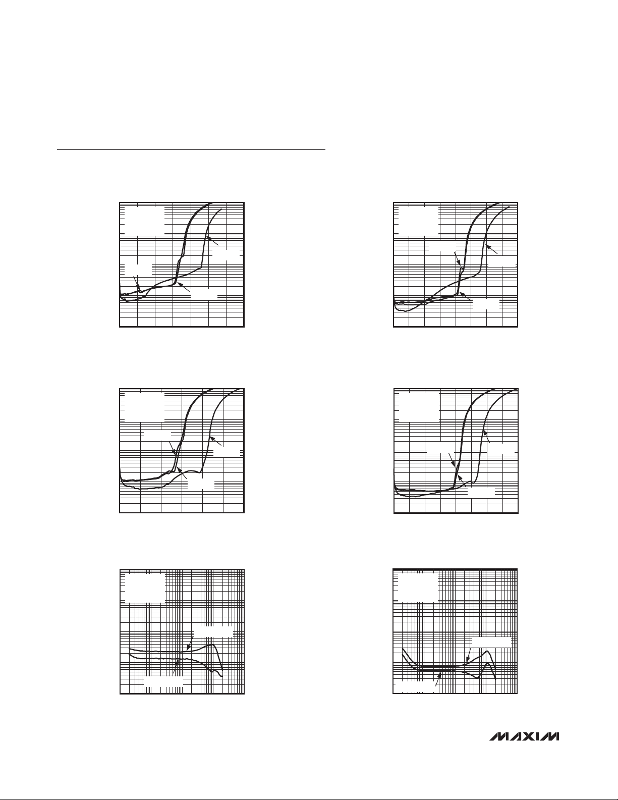
Conventional single-supply headphone amplifiers have
their outputs biased about a nominal DC voltage (typically half the supply) for maximum dynamic range.
Large-coupling capacitors are needed to block this DC
bias from the headphone. Without these capacitors, a
significant amount of DC current flows to the headphone, resulting in unnecessary power dissipation and
possible damage to both headphone and headphone
amplifier.
Maxim’s patented DirectDrive architecture uses a
charge pump to create an internal negative supply voltage, allowing the MAX9820 outputs to be biased at
DirectDrive Headphone Amplifier
with External Gain
8 _______________________________________________________________________________________
Pin Description
Table 1. Windows Vista Premium Mobile Specifications vs. MAX9820 Specifications
Note: THD+N, dynamic range, and crosstalk are measured in accordance with AES-17 audio measurements standards.
PIN NAME FUNCTION
1 C1P Flying Capacitor Positive Terminal. Connect a 1µF ceramic capacitor from C1P to C1N.
2 C1N Flying Capacitor Negative Terminal. Connect a 1µF ceramic capacitor from C1N to C1P.
3VSSCharge-Pump Output. Bypass with a 1µF capacitor to GND.
4 OUTL Left-Channel Output
5 OUTR Right-Channel Output
6 INR Right-Channel Input
7 INL Left-Channel Input
8VDDPositive Power-Supply Input. Bypass with a 10µF capacitor to GND.
9 SHDN Active-Low Shutdown Input
10 GND Signal Ground
—EP
Exposed Pad. Internally connected to GND. Connect to a large ground plane to maximize thermal
performance. Not intended as an electrical connection point.
DEVICE TYPE REQUIREMENT
Analog Line Output
Jack (R
FS = 0.707V
Analog Headphone
Out Jack (R
FS = 0.300V
= 10kΩ,
L
RMS
= 32Ω,
L
RMS
)
)
Dynamic range with signal
Dynamic range with signal
Headphone output crosstalk ≤ -50dB (20Hz, 15kHz) -73dB (20Hz, 15kHz)
THD+N ≤ -65dB FS (100Hz, 20kHz) -83dBFS (100Hz, 20kHz)
present
Line output crosstalk ≤ -50dB (20Hz, 15kHz) -73dB (20Hz, 15kHz)
THD+N ≤ -45dB FS (100Hz, 20kHz) -85dBFS (100Hz, 20kHz)
present
WINDOWS VISTA PREMIUM MOBILE
SPECIFICATIONS
≤ -80dBV, A-weighted (20Hz, 20kHz)
≤ -60dBV, A-weighted (20Hz, 20kHz)
TYPICAL PERFORMANCE
MAX9820
-101dB A-weighted
(20Hz, 20kHz)
-94dB A-weighted
(20Hz, 20kHz)
Page 9
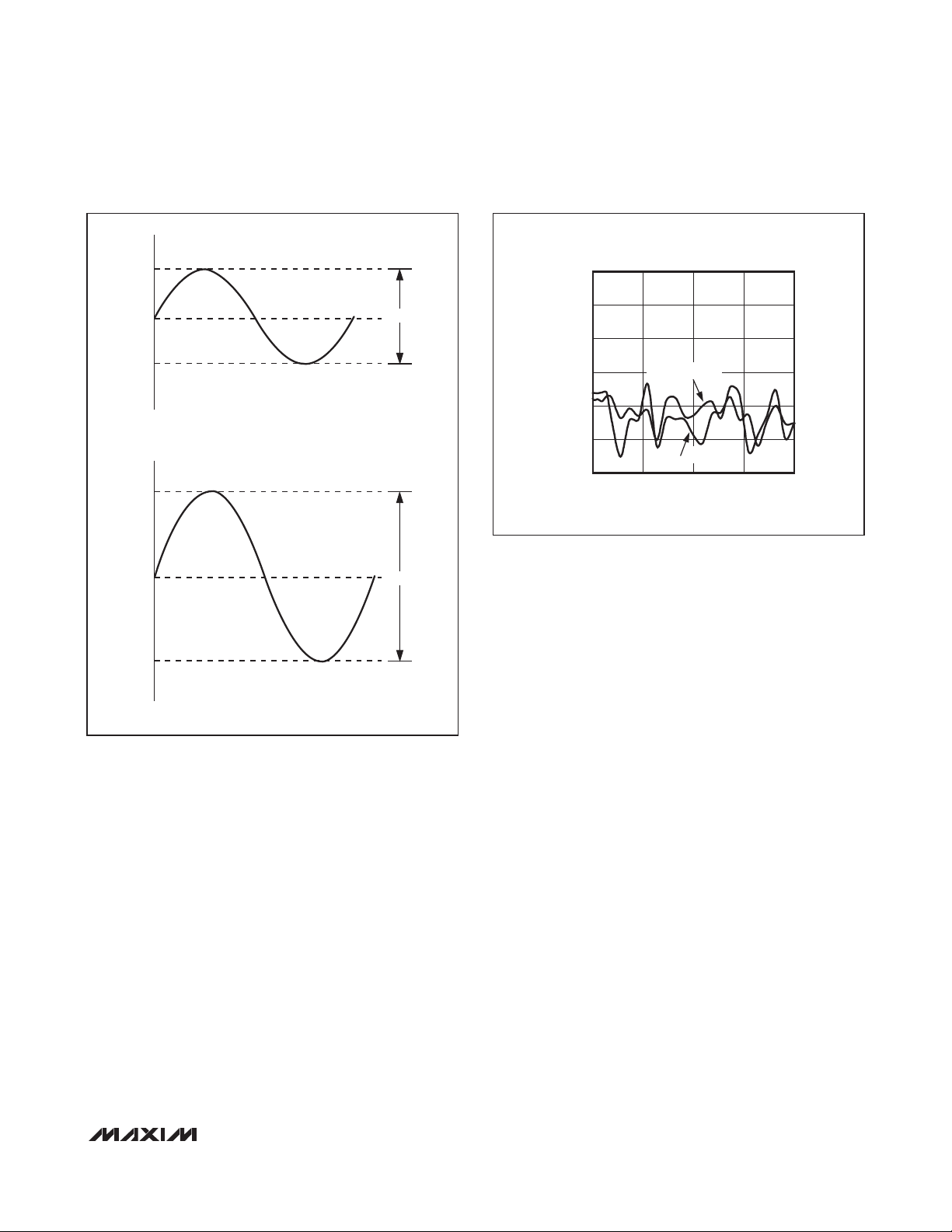
GND (Figure 1). With no DC component, there is no
need for the large DC-blocking capacitors. The
MAX9820 charge pump requires two small ceramic
capacitors, conserving board space, reducing cost,
and improving the frequency response of the headphone amplifier.
Charge Pump
The MAX9820 features a low-noise charge pump. The
500kHz (typ) charge pump switching frequency is well
beyond the audio range and does not interfere with
audio signals.
Click-and-Pop Suppression
In conventional single-supply audio amplifiers, the output-coupling capacitor contributes significantly to audible clicks and pops. Upon startup, the amplifier
charges the coupling capacitor to its bias voltage, typically half the supply. Likewise, on shutdown, the capacitor is discharged. This results in a DC shift across the
capacitor, which appears as an audible transient at the
speaker. Since DirectDrive biases the outputs at
ground, this problem does not arise. Additionally, the
MAX9820 features extensive click-and-pop suppression that eliminates any audible transient sources internal to the device.
RF Susceptibility
Modern audio systems are often subject to RF radiation
from sources such as wireless and cellular phone networks. Although the RF radiation is out of the audio
band, many signals, GSM signals in particular, contain
bursts or modulation at audible frequencies. Most analog amplifiers demodulate the low-frequency envelope,
adding noise to the audio signal. The MAX9820 architecture addresses the RF susceptibility problem by
rejecting RF noise and preventing it from coupling into
the audio band.
MAX9820
DirectDrive Headphone Amplifier
with External Gain
_______________________________________________________________________________________ 9
Figure 1. Conventional Driver Output Waveform vs. MAX9820
Output Waveform
Figure 2. MAX9820 RF Susceptibility
V
OUT
V
DD
V
/2
DD
GND
CONVENTIONAL DRIVER OUTPUT WAVEFORMS
V
OUT
V
DD
GND
-V
DD
MAX9820 OUTPUT WAVEFORMS
V
DD
2V
DD
RF IMMUNITY vs. FREQUENCY
0
-20
-40
-60
-80
RF IMMUNITY (dBV)
-100
-120
0.8 3.00
LEFT CHANNEL
RIGHT CHANNEL
FREQUENCY (GHz)
2.451.901.35
MAX9820 fig02
Page 10

MAX9820
Shutdown
The MAX9820 features a low-power shutdown mode
that reduces quiescent current consumption to less
than 1µA, extending battery life for portable applications. Drive SHDN low to disable the amplifiers and the
charge pump. In shutdown mode, the amplifier output
impedance is set to 600Ω || RFB. The amplifiers and
charge pump are enabled once SHDN is driven high.
Applications Information
Power Dissipation
Under normal operating conditions, linear power amplifiers can dissipate a significant amount of power. The
maximum power dissipation for each package is given
in the
Absolute Maximum Ratings
section or can be cal-
culated by the following equation:
where T
J(MAX)
is +150°C, TAis the ambient temperature, and θJAis the reciprocal of the derating factor in
°C/W as specified in the
Absolute Maximum Ratings
section.
The MAX9820 has two power dissipation sources: a
charge pump and the two output amplifiers. If power
dissipation for a given application exceeds the maximum allowed package power dissipation, reduce VDD,
increase load impedance, decrease the ambient temperature, or add heatsinking to the device. Large output, supply, and ground traces decrease θJA, allowing
more heat to be transferred from the package to the
surrounding air.
Thermal-overload protection limits total power dissipation in the MAX9820. When the junction temperature
exceeds 145°C (typ), the thermal protection circuitry
disables the amplifier output stage. The amplifiers are
enabled once the junction temperature cools by
approximately 15°C.
Undervoltage Lockout (UVLO)
The MAX9820 features a UVLO function that prevents
the device from operating if the supply voltage falls
below 2.2V (min). This feature ensures proper operation
during brownout conditions and prevents deep battery
discharge. Once the supply voltage reaches the minimum supply voltage range, the MAX9820 charge pump
is turned on and the amplifiers are powered, provided
that SHDN is high.
Component Selection
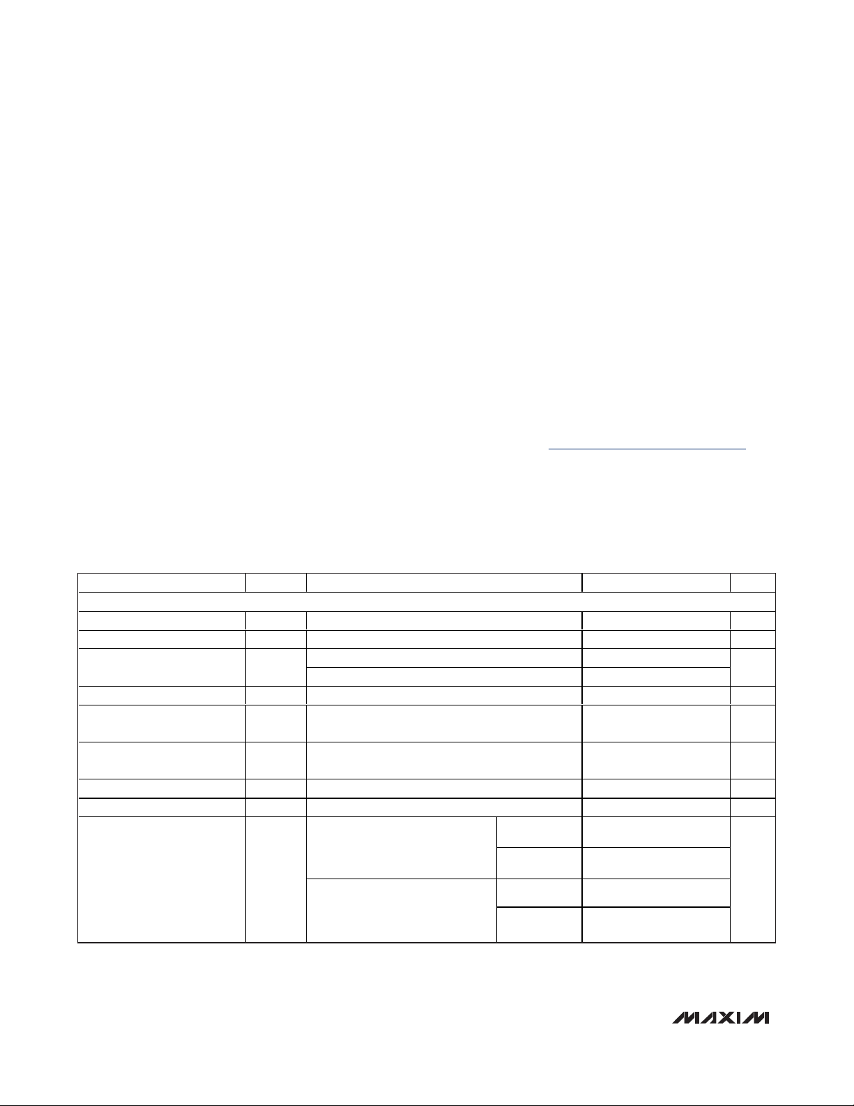
Input-Coupling Capacitor
The input capacitor (CIN), in conjunction with the input
resistor (RIN), forms a highpass filter that removes the
DC bias from an incoming signal (see the
Functional
Diagram/Typical Operating Circuit
). The AC-coupling
capacitor allows the device to bias the signal to an optimum DC level. Assuming zero-source impedance, the
-3dB point of the highpass filter is given by:
Choose the CINsuch that f
-3dB
is well below the lowest
frequency of interest. Setting f
-3dB
too high affects the
device’s low-frequency response. Use capacitors
whose dielectrics have low-voltage coefficients, such
as tantalum or aluminum electrolytic. Capacitors with
high-voltage coefficients, such as ceramics, can result
in increased distortion at low frequencies.
Charge-Pump Capacitor Selection
Use ceramic capacitors with a low ESR for optimum
performance. For optimal performance over the extended temperature range, select capacitors with an X7R or
X5R dielectric. Table 2 lists suggested manufacturers.
DirectDrive Headphone Amplifier
with External Gain
10 ______________________________________________________________________________________
Table 2. Suggested Capacitor Vendors
P
DISSPKG MAX
()
TT
=
−
J MAX A
()
θ
JA
f
dB
−=3
2π
RC
1
IN IN
SUPPLIER PHONE FAX WEBSITE
Taiyo Yuden 800-348-2496 847-925-0899 www.t-yuden.com
TDK 847-803-6100 847-390-4405 www.component.tdk.com
Murata 770-436-1300 770-436-3030 www.murata.com
Page 11

Amplifier Gain
The gain of the MAX9820 is set externally using input
and feedback resistors (see the
Functional Diagram/
Typical Operating Circuit
). The gain is:
Choose feedback resistor values in the tens of kΩ
range.
Layout and Grounding
Proper layout and grounding are essential for optimum
performance. Connect EP and GND together at a single
point on the PCB. Ensure ground return resistance is
minimized for optimum crosstalk performance. Place
the power-supply bypass capacitor, the charge-pump
hold capacitor, and the charge-pump flying capacitor
as close as possible to the MAX9820. Route all traces
that carry switching transients away from the audio signal path.
MAX9820
DirectDrive Headphone Amplifier
with External Gain
______________________________________________________________________________________ 11
Chip Information
PROCESS: BiCMOS
Functional Diagram/Typical Operating Circuit
R
A
=− (/ )
V
R
FB
VV
IN
C
IN
1.0µF
OFF
ON
2.7V TO 5.5V
C3
10µF
C1
1.0µF
SHDN
V
DD
8
1
C1P
C1N
2
UVLO/SHUTDOWN
CONTROL
CHARGE
PUMP
R
IN
40.2kΩ
CLICK-AND-POP
SUPPRESSION
7
INL
TO V
-1
-1
TO V
40.2kΩ
DD
TO V
DD
R
FB
4
OUTL
HEADPHONE
JACK
SS
OUTR
5
GND
1093
V
SS
C2
1.0µF
C
1.0µF
R
IN
IN
40.2kΩ
INR
6
R
FB
40.2kΩ
Page 12

MAX9820
DirectDrive Headphone Amplifier
with External Gain
12 ______________________________________________________________________________________
PACKAGE TYPE PACKAGE CODE DOCUMENT NO.
10 TDFN-EP T1033+1
21-0137
Package Information
For the latest package outline information and land patterns, go to www.maxim-ic.com/packages.
6, 8, &10L, DFN THIN.EPS
Page 13

MAX9820
DirectDrive Headphone Amplifier
with External Gain
Maxim cannot assume responsibility for use of any circuitry other than circuitry entirely embodied in a Maxim product. No circuit patent licenses are
implied. Maxim reserves the right to change the circuitry and specifications without notice at any time.
Maxim Integrated Products, 120 San Gabriel Drive, Sunnyvale, CA 94086 408-737-7600 ____________________
13
© 2009 Maxim Integrated Products Maxim is a registered trademark of Maxim Integrated Products, Inc.
Package Information (continued)
For the latest package outline information and land patterns, go to www.maxim-ic.com/packages.
COMMON DIMENSIONS
SYMBOL MIN. MAX.
A 0.70 0.80
D 2.90 3.10
E 2.90 3.10
0.00 0.05
A1
L 0.20 0.40
0.25 MIN.k
A2 0.20 REF.
PACKAGE VARIATIONS
PKG. CODE N D2 E2 e JEDEC SPEC b
T633-2 6 1.50±0.10 2.30±0.10 0.95 BSC MO229 / WEEA 0.40±0.05 1.90 REF
T833-2 8 1.50±0.10 2.30±0.10 0.65 BSC MO229 / WEEC 0.30±0.05 1.95 REF
T833-3 8 1.50±0.10 2.30±0.10 0.65 BSC MO229 / WEEC 0.30±0.05 1.95 REF
1.50±0.10 MO229 / WEED-3
2.30±0.10 MO229 / WEED-3 2.00 REF0.25±0.050.50 BSC1.50±0.1010T1033-2
0.40 BSC - - - - 0.20±0.05 2.40 REFT1433-2 14 2.30±0.101.70±0.10
[(N/2)-1] x e
2.00 REF0.25±0.050.50 BSC2.30±0.1010T1033-1
2.40 REF0.20±0.05- - - - 0.40 BSC1.70±0.10 2.30±0.1014T1433-1
 Loading...