

Page 1
General Description
The MAX9770 combines a mono, filterless, Class D
speaker amplifier and stereo DirectDrive headphone
amplifiers in a single device. The MAX9770 operates
from a single 2.5V to 5.5V supply and includes features
that reduce external component count, system cost,
board space, and offer improved audio reproduction.
The speaker amplifier makes use of Maxim’s patented
Class D architecture, providing Class AB performance
with Class D efficiency, conserving board space, and
extending battery life. The speaker amplifier delivers
1.2W into an 8Ω load while offering efficiencies above
85%. A spread-spectrum scheme reduces radiated
emissions caused by the modulation frequency.
Furthermore, the MAX9770 oscillator can be synchronized to an external clock through the SYNC input,
avoiding possible problem frequencies inside a system.
The speaker amplifier features a low 0.025% THD+N,
high 70dB PSRR, and SNR in excess of 90dB.
The headphone amplifiers feature Maxim’s patented
DirectDrive architecture that produces a ground-referenced output from a single supply, eliminating the need
for large DC-blocking capacitors. The headphone amplifiers deliver up to 80mW into a 16Ω load, feature low
0.015% THD+N, high 80dB PSRR, and ±8kV ESD-protected outputs. A headphone sense input detects the
presence of a headphone, and automatically configures
the amplifiers for either speaker or headphone mode.
The MAX9770 includes internally set, logic-selectable
gain, and a comprehensive input multiplexer/mixer, allowing multiple audio sources to be selected and for true
mono reproduction of a stereo source in speaker mode.
Industry-leading click-and-pop suppression eliminates
audible transients during power and shutdown cycles. A
low-power shutdown mode decreases supply current
consumption to 0.1µA, further extending battery life.
The MAX9770 is offered in space-saving, thermally efficient 28-pin TQFN (5mm x 5mm x 0.8mm) and 28-pin
TSSOP packages. The MAX9770 features thermal-overload and output short-circuit protection, and is specified
over the extended -40°C to +85°C temperature range.
Applications
Cellular Phones
PDAs
Compact Notebooks
Features
♦ 1.2W Filterless Class D Amplifier Passes FCC
Class B Radiated Emissions Standards with
100mm of Cable
♦ Unique Spread-Spectrum Mode Offers 5dB
Emissions Improvement Over Conventional
Methods
♦ 80mW DirectDrive Headphone Amplifier
Eliminates Bulky DC-Blocking Capacitors
♦ High 80dB PSRR at 217Hz
♦ 85% Efficiency
♦ Low 0.015% THD+N
♦ Industry-Leading Click-and-Pop Suppression
♦ Integrated 3-Way Input Mixer/Multiplexer
♦ Logic-Selectable Gain
♦ Short-Circuit and Thermal Protection
♦ ±8kV ESD-Protected Headphone Outputs
♦ Low-Power Shutdown Mode
♦ Available in Space-Saving, Thermally Efficient
Packages
28-Pin TQFN (5mm x 5mm x 0.8mm)
28-Pin TSSOP
MAX9770
1.2W Low-EMI, Filterless, Mono Class D Amplifier
with Stereo Dir ectDrive Headphone Amplifiers
________________________________________________________________ Maxim Integrated Products 1
SPKR
(MONO)
MAX9770
CLASS
D
V
DD
DirectDrive
STEREO
HEADPHONE
L1IN
L2IN
R1IN
R2IN
MONO
GAIN SEL
INPUT SEL
MUTE
SHDN
HPS
Ordering Information
Simplified Block Diagram
19-3134; Rev 0; 5/04
For pricing, delivery, and ordering information, please contact Maxim/Dallas Direct! at
1-888-629-4642, or visit Maxim’s website at www.maxim-ic.com.
Pin Configuration appears at end of data sheet.
†
Lead-free package.
*EP = Exposed paddle.
PART TEMP RANGE PIN-PACKAGE
MAX9770ETI
MAX9770EUI -40oC to +85oC 28 TSSOP
†
-40oC to +85oC 28 TQFN-EP*
Page 2
MAX9770
1.2W Low-EMI, Filterless, Mono Class D Amplifier
with Stereo Dir ectDrive Headphone Amplifiers
2 _______________________________________________________________________________________
ABSOLUTE MAXIMUM RATINGS
ELECTRICAL CHARACTERISTICS
(VDD= PVDD= CPVDD= 3.3V, GND = PGND = CPGND = 0V, SHDN = 3.3V, C1 = C2 = 1µF, C
BIAS
= 0.047µF, SYNC = GND, RL= ∞,
speaker load connected between OUT+ and OUT-, headphone load connected between HPOUT_ and GND, T
A
= T
MIN
to T
MAX
,
unless otherwise noted. Typical values are at T
A
= +25°C.) (Notes 1, 2)
Stresses beyond those listed under “Absolute Maximum Ratings” may cause permanent damage to the device. These are stress ratings only, and functional
operation of the device at these or any other conditions beyond those indicated in the operational sections of the specifications is not implied. Exposure to
absolute maximum rating conditions for extended periods may affect device reliability.
GND to PGND to CPGND......................................-0.3V to +0.3V
V
DD
to PVDDto CPVDD..........................................-0.3V to +0.3V
V
DD
to GND..............................................................................6V
PV
DD
to PGND .........................................................................6V
CPV
DD
to CPGND....................................................................6V
CPV
SS
to CPGND....................................................................-6V
SV
SS
to GND...........................................................................-6V
C1N..........................................(PV
SS
- 0.3V) to (CPGND + 0.3V)
HPOUT_ to GND ....................................................................±3V
All other pins to GND..................................-0.3V to (V
DD
+ 0.3V)
Continuous Current Into/Out of:
PV
DD
, PGND, OUT_......................................................600mA
PV
SS
..............................................................................260mA
Duration of HPOUT_ Short Circuit to V
DD
, PVDD,
GND, PGND...........................................................Continuous
Duration of Short Circuit between
HPOUTL and HPOUTR ..........................................Continuous
Duration of OUT_ Short Circuit to V
DD
, PVDD, GND, PGND ..10s
Duration of Short Circuit Between OUT+ and OUT-...............10s
Continuous Power Dissipation (T
A
= +70°C)
28-Pin TQFN (derate 20.8mW/°C above +70°C) .......1667mW
28-Pin TSSOP (derate 12.8mW°C above +70°C) ......1026mW
Junction Temperature......................................................+150°C
Operating Temperature Range ...........................-40°C to +85°C
Storage Temperature Range.............................-65°C to +150°C
Lead Temperature (soldering, 10s).................................+300°C
PARAMETER
CONDITIONS MIN TYP
UNITS
GENERAL
Supply Voltage Range V
DD
Inferred from PSRR test 2.5 5.5 V
Headphone mode 5.5 10
Quiescent Supply Current I
DD
No load
Speaker mode 5.2 7.5
mA
Shutdown Supply Current I
SHDN
SHDN = HPS = GND 0.1 10 µA
Shutdown to Full Operation t
ON
50 ms
MONO 7 10
Input Impedance R
IN
(Note 3)
INL_, INR_ 14 20
kΩ
Bias Voltage V
BIAS
1.1 1.25 1.4 V
Feedthrough
From any unselected input to any output,
f = 10kHz
70 dB
SPEAKER AMPLIFIER (GAIN1 = GAIN2 = VDD, HPS = GND)
Output Offset Voltage V
OS
±15 ±70 mV
VDD = 2.5V to 5.5V 50 70
70
68
Power-Supply Rejection Ratio PSRR
50
dB
RL = 8Ω 550
RL = 4Ω 900
Output Power P
OUT
f = 1kHz,
THD+N = 1%,
GAIN1 = 1,
GAIN2 = 0
V
DD
= 5V RL = 8Ω 1200
mW
RL = 8Ω, P
OUT
= 300mW, f = 1kHz
Total Harmonic Distortion Plus
Noise
RL = 4Ω, P
OUT
= 300mW, f = 1kHz 0.03
%
SYMBOL
MAX
THD+N
V
= 200mV
(Note 4)
RIPPLE
V
= 200mV
RIPPLE
V
= 200mV
RIPPLE
VDD = 3.3V
, f = 217Hz
P-P
, f = 1kHz
P-P
, f = 20kHz
P-P
0.025
Page 3
MAX9770
1.2W Low-EMI, Filterless, Mono Class D Amplifier
with Stereo Dir ectDrive Headphone Amplifiers
_______________________________________________________________________________________ 3
ELECTRICAL CHARACTERISTICS (continued)
(VDD= PVDD= CPVDD= 3.3V, GND = PGND = CPGND = 0V, SHDN = 3.3V, C1 = C2 = 1µF, C
BIAS
= 0.047µF, SYNC = GND, RL= ∞,
speaker load connected between OUT+ and OUT-, headphone load connected between HPOUT_ and GND, T
A
= T
MIN
to T
MAX
,
unless otherwise noted. Typical values are at T
A
= +25°C.) (Notes 1, 2)
PARAMETER
CONDITIONS MIN TYP
UNITS
Signal-to-Noise Ratio SNR RL = 8Ω, V
OUT
= 2V
RMS
, A-weighted 85.9 dB
SYNC = GND 980 1100
SYNC = FLOAT
1450
Output Switching Frequency F
S
SYNC = V
DD
1220
kHz
SYNC Frequency Lock Range 800
kHz
Efficiency η PO = 1000mW, f = 1kHz 85 %
GAIN1 = 0, GAIN2 = 0 6
GAIN1 = 0, GAIN2 = 1 3
GAIN1 = 1, GAIN2 = 0 9
Gain A
V
GAIN1 = 1, GAIN2 = 1 0
dB
Gain Accuracy ±5%
Speaker Path Off-Isolation
HPS = V
DD
, headphone amplifier active,
f = 1kHz
102 dB
HEADPHONE AMPLIFIER (GAIN1 = 1, GAIN2 = 0, HPS = V
DD
)
Output Offset Voltage V
OS
±5 ±10 mV
VDD = 2.5V to 5.5V 65 76
85
V
RIPPLE
= 200mV
P-P
, f = 1kHz 82
Power-Supply Rejection Ratio PSRR
56
dB
RL = 32Ω 40 55
RL = 16Ω 40
RL = 32Ω 60
Output Power P
OUT
f = 1kHz,
THD+N = 1%
V
DD
= 5V
R
L
= 16Ω 80
mW
RL = 32Ω, P
OUT
= 50mW, f = 1kHz
Total Harmonic Distortion Plus
Noise
RL = 16Ω, P
OUT
= 35mW, f = 1kHz 0.03
%
Signal-to-Noise Ratio SNR
R
L
= 32Ω, V
OUT
= 300mV
RMS
,
BW = 22Hz to 22kHz
101 dB
Crosstalk
Between channels, f = 1kHz,
V
IN
= 200mV
P-P
80 dB
Headphone Off-Isolation
HPS = GND, speaker amplifier active,
f = 1kHz
96 dB
SYMBOL
(Note 3)
THD+N
V
= 200mV
V
RIPPLE
= 200mV
RIPPLE
VDD = 3.3V
P-P
P-P
, f = 217kHz
, f = 20kHz
1280
±120kHz
0.015
MAX
1220
1620
2000
Page 4
10
0.001
10 100 10k 100k
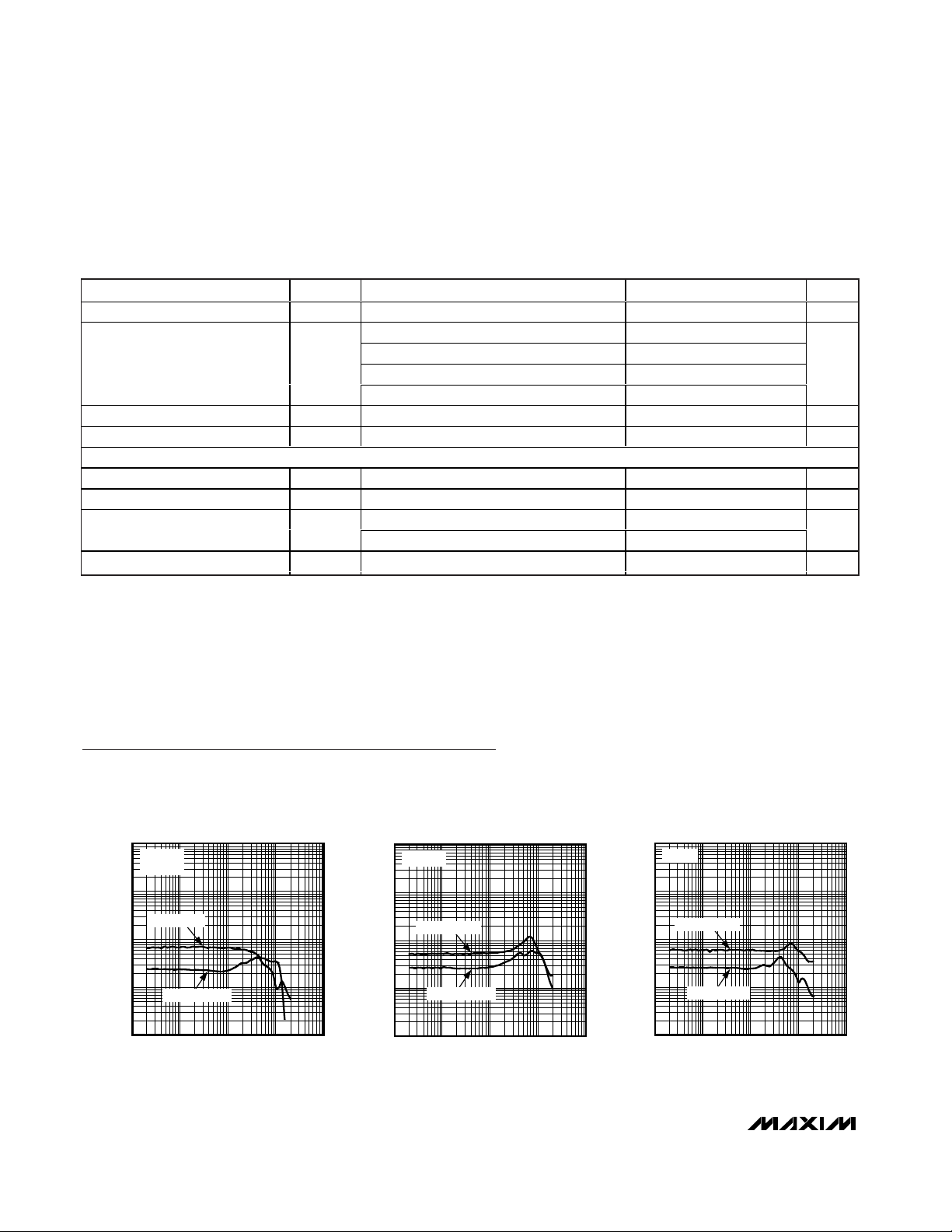
TOTAL HARMONIC DISTORTION PLUS NOISE
vs. FREQUENCY (SPEAKER MODE)
0.01
0.1
1
MAX9770 toc01
FREQUENCY (Hz)
THD+N (%)
1k
VDD = +5V
R
L
= 4
Ω
P
OUT
= 25mW
P
OUT
= 1000mW
10
0.001
10 100 10k 100k
TOTAL HARMONIC DISTORTION PLUS NOISE
vs. FREQUENCY (SPEAKER MODE)
0.01
0.1
1
MAX9770 toc02
FREQUENCY (Hz)
THD+N (%)
1k
RL = 4
Ω
P
OUT
= 100mW
P
OUT
= 500mW
10
0.001
10 100 10k 100k
TOTAL HARMONIC DISTORTION PLUS NOISE
vs. FREQUENCY (SPEAKER MODE)
0.01
0.1
1
MAX9770 toc03
FREQUENCY (Hz)
THD+N (%)
1k
RL = 8
Ω
P
OUT
= 40mW
P
OUT
= 400mW
Typical Operating Characteristics
(VDD= 3.3V, BW = 22Hz to 22kHz, GAIN1 = 1, GAIN2 = 0, spread-spectrum mode, headphone outputs in phase.)
MAX9770
1.2W Low-EMI, Filterless, Mono Class D Amplifier
with Stereo Dir ectDrive Headphone Amplifiers
4 _______________________________________________________________________________________
ELECTRICAL CHARACTERISTICS (continued)
(VDD= PVDD= CPVDD= 3.3V, GND = PGND = CPGND = 0V, SHDN = 3.3V, C1 = C2 = 1µF, C
BIAS
= 0.047µF, SYNC = GND, RL= ∞,
speaker load connected between OUT+ and OUT-, headphone load connected between HPOUT_ and GND, T
A
= T
MIN
to T
MAX
,
unless otherwise noted. Typical values are at T
A
= +25°C.) (Notes 1, 2)
PARAMETER
CONDITIONS MIN TYP
UNITS
Capacitive-Load Drive C
L
1000 pF
GAIN1 = 0, GAIN2 = 0 7
GAIN1 = 0, GAIN2 = 1 4
GAIN1 = 1, GAIN2 = 0 -2
Gain A
V
GAIN1 = 1, GAIN2 = 1 1
dB
Gain Accuracy
%
ESD Protection HPOUTR, HPOUTL, IEC Air Discharge ±8kV
DIGITAL INPUTS (SHDN, SYNC, HPS, GAIN_, SEL_)
Input Voltage High V
IH
2V
Input Voltage Low V
IL
0.8 V
SYNC input ±25
Input Leakage Current
All other logic inputs ±1
µA
HPS Input Current HPS = GND -10 µA
Note 1: All devices are 100% production tested at +25°C. All temperature limits are guaranteed by design.
Note 2: Speaker amplifier testing performed with a resistive load in series with an inductor to simulate an actual speaker load. For
R
L
= 4Ω, L = 47µH. For RL= 8Ω, L = 68µH.
Note 3: Guaranteed by design, not production tested.
Note 4: PSRR is specified with the amplifier inputs connected to GND through C
IN
.
SYMBOL
MAX
±2.5
Page 5
MAX9770
1.2W Low-EMI, Filterless, Mono Class D Amplifier
with Stereo Dir ectDrive Headphone Amplifiers
_______________________________________________________________________________________ 5
10
0.001
10 100 10k 100k
TOTAL HARMONIC DISTORTION PLUS NOISE
vs. FREQUENCY (SPEAKER MODE)
0.01
0.1
1
MAX9770 toc04
FREQUENCY (Hz)
THD+N (%)
1k
VDD = 5V
P
OUT
= 1W
R
L
= 8
Ω
SSM MODE
FFM MODE
100
0
400 800 1200
1600
10
1
0.1
0.01
0.001
TOTAL HARMONIC DISTORTION PLUS NOISE
vs. OUTPUT POWER (SPEAKER MODE)
MAX9770 toc05
OUTPUT POWER (mW)
THD+N (%)
VDD = 5V
R
L
= 8
Ω
f = 20Hz
f = 1kHz
f = 10kHz
100
0
200 600
400
800
1000
10
1
0.1
0.01
0.001
TOTAL HARMONIC DISTORTION PLUS NOISE
vs. OUTPUT POWER (SPEAKER MODE)
MAX9770 toc06
OUTPUT POWER (mW)
THD+N (%)
f = 20Hz
f = 1kHz
f = 10kHz
RL = 4
Ω
100
0
200 400 600
800
10
1
0.1
0.01
0.001
TOTAL HARMONIC DISTORTION PLUS NOISE
vs. OUTPUT POWER (SPEAKER MODE)
MAX9770 toc07
OUTPUT POWER (mW)
THD+N (%)
RL = 8
Ω
f = 20Hz
f = 1kHz
f = 10kHz
100
0
400 800 1200
1600
10
1
0.1
0.01
0.001
TOTAL HARMONIC DISTORTION PLUS NOISE
vs. OUTPUT POWER (SPEAKER MODE)
MAX9770 toc08
OUTPUT POWER (mW)
THD+N (%)
VDD = 5V
f = 1kHz
R
L
= 8
Ω
SSM MODE
FFM MODE
1.75
0
110100
OUTPUT POWER
vs. LOAD RESISTANCE (SPEAKER MODE)
0.50
0.25
MAX9770 toc09
LOAD RESISTANCE (Ω)
OUTPUT POWER (W)
0.75
1.00
1.25
1.50
VDD = 5V
f = 1kHz
THD+N = 10%
THD+N = 1%
1.0
0
110100
OUTPUT POWER
vs. LOAD RESISTANCE (SPEAKER MODE)
0.2
MAX9770 toc10
LOAD RESISTANCE (Ω)
OUTPUT POWER (W)
0.4
0.6
0.8
f = 1kHz
THD+N = 10%
THD+N = 1%
2.0
1.5
1.0
0.5
0
2.5 4.03.0 3.5 4.5 5.0 5.5
OUTPUT POWER
vs. SUPPLY VOLTAGE (SPEAKER MODE)
MAX9770 toc11
SUPPLY VOLTAGE (V)
OUTPUT POWER (W)
f = 1kHz
R
L
= 8
Ω
THD+N = 10%
THD+N = 1%
0
30
20
10
50
40
90
80
70
60
100
0 0.2 0.4 0.6 0.8 1.0 1.2 1.4
EFFICIENCY vs. OUTPUT POWER
MAX9770 toc12
OUTPUT POWER (W)
EFFICIENCY (%)
VDD = 5V
f = 1kHz
R
L
= 8Ω
Typical Operating Characteristics (continued)
(VDD= 3.3V, BW = 22Hz to 22kHz, GAIN1 = 1, GAIN2 = 0, spread-spectrum mode, headphone outputs in phase.)
Page 6
MAX9770
1.2W Low-EMI, Filterless, Mono Class D Amplifier
with Stereo Dir ectDrive Headphone Amplifiers
6 _______________________________________________________________________________________
Typical Operating Characteristics (continued)
(VDD= 3.3V, BW = 22Hz to 22kHz, GAIN1 = 1, GAIN2 = 0, spread-spectrum mode, headphone outputs in phase.)
0
30
20
10
40
50
60
70
80
90
100
00.40.2 0.6 0.8 1.0
EFFICIENCY vs. OUTPUT POWER
MAX9770 toc13
OUTPUT POWER (W)
EFFICIENCY (%)
RL = 8Ω
RL = 4Ω
f = 1kHz
0
-10
-20
-30
-40
-50
-60
-70
-80
10 1k 10k100 100k
POWER-SUPPLY REJECTION RATIO
vs. FREQUENCY (SPEAKER MODE)
MAX9770 toc14
FREQUENCY (Hz)
PSRR (dB)
V
RIPPLE
= 200mV
P-P
RL = 8Ω
-140
-100
-120
-60
-80
-20
-40
0
OUTPUT SPECTRUM
(SPEAKER MODE)
MAX9770 toc15
FREQUENCY (kHz)
MAGNITUDE (dB)
0510
15
20
RL = 8Ω
f = 1kHz
FFM MODE
V
IN
= -60dBV
-140
-100
-120
-60
-80
-20
-40
0
OUTPUT SPECTRUM
(SPEAKER MODE)
MAX9770 toc16
FREQUENCY (kHz)
MAGNITUDE (dB)
0510
15
20
RL = 8Ω
f = 1kHz
SSM MODE
V
IN
= -60dBV
-160
-100
-120
-140
-60
-80
-20
-40
0
OUTPUT SPECTRUM
(SPEAKER MODE)
MAX9770 toc17
FREQUENCY (kHz)
MAGNITUDE (dB)
0510
15
20
RL = 8Ω
f = 1kHz
SSM MODE
A-WEIGHTED
V
IN
= -60dBV
0
-100
1M 10M 100M
WIDEBAND OUTPUT SPECTRUM
(SPEAKER MODE)
-80
MAX9770 toc18
FREQUENCY (Hz)
MAGNITUDE (dB)
-60
-40
-20
-30
-50
-70
-90
-10
FFM MODE
RBW = 10kHz
0
-100
1M 10M 100M
WIDEBAND OUTPUT SPECTRUM
(SPEAKER MODE)
-80
MAX9770 toc19
FREQUENCY (Hz)
MAGNITUDE (dB)
-60
-40
-20
-30
-50
-70
-90
-10
SSM MODE
RBW = 10kHz
STARTUP WAVEFORM
(SPEAKER MODE)
MAX9770 toc20
4ms/div
2V/divSHDN
OUT+ - OUT-
500mV/div
RL = 8Ω
f = 1kHz
MIXER OUTPUT
MAX9770 toc21
400µs/div
10kHz
1V/div
4kHz
1V/div
1kHz
2V/div
IN_1
IN_2
MONO
OUT
1V/div
Page 7
MAX9770
1.2W Low-EMI, Filterless, Mono Class D Amplifier
with Stereo Dir ectDrive Headphone Amplifiers
_______________________________________________________________________________________ 7
10
0.001
10 100 10k 100k
TOTAL HARMONIC DISTORTION PLUS NOISE
vs. FREQUENCY (HEADPHONE MODE)
0.01
0.1
1
MAX9770 toc22
FREQUENCY (Hz)
THD+N (%)
1k
P
OUT
= 10mW
P
OUT
= 50mW
VDD = 5V
R
L
= 16Ω
10
0.001
10 100 10k 100k
TOTAL HARMONIC DISTORTION PLUS NOISE
vs. FREQUENCY (HEADPHONE MODE)
0.01
0.1
1
MAX9770 toc23
FREQUENCY (Hz)
THD+N (%)
1k
P
OUT
= 10mW
P
OUT
= 50mW
VDD = 5V
R
L
= 32Ω
10
0.001
10 100 10k 100k
TOTAL HARMONIC DISTORTION PLUS NOISE
vs. FREQUENCY (HEADPHONE MODE)
0.01
0.1
1
MAX9770 toc24
FREQUENCY (Hz)
THD+N (%)
1k
P
OUT
= 10mW
P
OUT
= 35mW
RL = 16Ω
10
0.001
10 100 10k 100k
TOTAL HARMONIC DISTORTION PLUS NOISE
vs. FREQUENCY (HEADPHONE MODE)
0.01
0.1
1
MAX9770 toc25
FREQUENCY (Hz)
THD+N (%)
1k
P
OUT
= 10mW
P
OUT
= 50mW
RL = 32Ω
100
10
1
0.1
0.01
0.001
0408020 60 100
TOTAL HARMONIC DISTORTION PLUS NOISE
vs. OUTPUT POWER (HEADPHONE MODE)
MAX9770 toc26
OUTPUT POWER (mW)
THD+N (%)
VDD = 5V
R
L
= 16Ω
f = 1kHz
f = 20Hz
f = 10kHz
100
10
1
0.1
0.01
0.001
0
60
20 40 80
TOTAL HARMONIC DISTORTION PLUS NOISE
vs. OUTPUT POWER (HEADPHONE MODE)
MAX9770 toc27
OUTPUT POWER (mW)
THD+N (%)
f = 20Hz
VDD = 5V
R
L
= 32Ω
f = 1kHz
f = 10kHz
100
10
1
0.1
0.01
0.001
0
50
40
2010
30 60
TOTAL HARMONIC DISTORTION PLUS NOISE
vs. OUTPUT POWER (HEADPHONE MODE)
MAX9770 toc28
OUTPUT POWER (mW)
THD+N (%)
RL = 16Ω
f = 1kHz
f = 10kHz
f = 20Hz
100
10
1
0.1
0.01
0.001
0
60
20 40 80
TOTAL HARMONIC DISTORTION PLUS NOISE
vs. OUTPUT POWER (HEADPHONE MODE)
MAX9770 toc29
OUTPUT POWER (mW)
THD+N (%)
f = 20Hz
RL = 32Ω
f = 1kHz
f = 10kHz
100
90
80
70
60
50
40
30
20
10
0
10 100 1000
OUTPUT POWER
vs. LOAD RESISTANCE (HEADPHONE MODE)
MAX9770 toc30
LOAD RESISTANCE (Ω)
OUTPUT POWER (mW)
VDD = 5V
f = 1kHz
THD+N = 10%
THD+N = 1%
Typical Operating Characteristics (continued)
(VDD= 3.3V, BW = 22Hz to 22kHz, GAIN1 = 1, GAIN2 = 0, spread-spectrum mode, headphone outputs in phase.)
Page 8
MAX9770
1.2W Low-EMI, Filterless, Mono Class D Amplifier
with Stereo Dir ectDrive Headphone Amplifiers
8 _______________________________________________________________________________________
Typical Operating Characteristics (continued)
(VDD= 3.3V, BW = 22Hz to 22kHz, GAIN1 = 1, GAIN2 = 0, spread-spectrum mode, headphone outputs in phase.)
80
70
60
50
40
30
20
10
0
10 100 1000
OUTPUT POWER
vs. LOAD RESISTANCE (HEADPHONE MODE)
MAX9770 toc31
LOAD RESISTANCE (Ω)
OUTPUT POWER (mW)
f = 1kHz
THD+N = 10%
THD+N = 1%
0
30
20
10
40
50
60
70
80
90
100
2.5 3.53.0 4.0 4.5 5.0 5.5
OUTPUT POWER
vs. SUPPLY VOLTAGE (HEADPHONE MODE)
MAX9770 toc32
SUPPLY VOLTAGE (V)
OUTPUT POWER (mW)
RL = 16Ω
f = 1kHz
THD+N = 10%
THD+N = 1%
0
10
20
30
40
50
60
70
80
2.5 3.53.0 4.0 4.5 5.0 5.5
OUTPUT POWER
vs. SUPPLY VOLTAGE (HEADPHONE MODE)
MAX9770 toc33
SUPPLY VOLTAGE (V)
OUTPUT POWER (mW)
RL = 32Ω
f = 1kHz
THD+N = 10%
THD+N = 1%
0
50
100
150
200
250
300
06030 90 120 150
POWER DISSIPATION
vs. OUTPUT POWER (HEADPHONE MODE)
MAX9770 toc34
OUTPUT POWER (mW)
POWER DISSIPATION (mW)
f = 1kHz
P
OUT
= P
OUTL
+ P
OUTR
RL = 16Ω
RL = 32Ω
0
-100
10 100 1k 10k 100k
POWER-SUPPLY REJECTION RATIO
vs. FREQUENCY (HEADPHONE MODE)
-80
MAX9770 toc35
FREQUENCY (Hz)
PSRR (dB)
-60
-40
-20
-30
-50
-70
-90
-10
VDD = 5V
V
RIPPLE
= 200mV
P-P
RL = 32Ω
0
-100
10 100 1k 10k 100k
CROSSTALK vs. FREQUENCY
(HEADPHONE MODE)
-80
MAX9770 toc36
FREQUENCY (Hz)
CROSSTALK (dB)
-60
-40
-20
-30
-50
-70
-90
-10
RL = 32Ω
f = 1kHz
V
IN
= 200mV
P-P
LEFT TO RIGHT
RIGHT TO LEFT
0
-100
10 100 1k 10k 100k
FEEDTHROUGH vs. FREQUENCY
-80
MAX9770 toc37
FREQUENCY (Hz)
FEEDTHROUGH (dB)
-60
-40
-20
-30
-50
-70
-90
-10
SEL1 = 0
SEL2 = 1
IN1_ = GND
IN2_ = DRIVEN
V
IN
= 2V
P-P
HEADPHONE MODE
SPEAKER MODE
0
10
30
20
50
40
60
20 30 40 50
OUTPUT POWER
vs. CHARGE-PUMP CAPACITANCE
MAX9770 toc38
LOAD (Ω)
OUTPUT POWER (mW)
C1 = C2 = 1µF
C1 = C2 = 0.47µF
f = 1kHz
THD+N = 1%
-140
-100
-120
-60
-80
-20
-40
0
OUTPUT SPECTRUM
(HEADPHONE MODE)
MAX9770 toc39
FREQUENCY (kHz)
MAGNITUDE (dB)
0 5 10 15 20
RL = 32Ω
f = 1kHz
V
IN
= -60dBV
Page 9

MAX9770
1.2W Low-EMI, Filterless, Mono Class D Amplifier
with Stereo Dir ectDrive Headphone Amplifiers
_______________________________________________________________________________________ 9
EXITING SHUTDOWN
(HEADPHONE MODE)
MAX9770 toc40
2µs/div
2V/divSHDN
OUT_
10mV/div
RL = 32Ω
ENTERING SHUTDOWN
(HEADPHONE MODE)
MAX9770 toc41
2µs/div
2V/divSHDN
OUT_
10mV/div
RL = 32Ω
0
2
6
4
8
10
SUPPLY CURRENT
vs. SUPPLY VOLTAGE
MAX9770 toc42
SUPPLY VOLTAGE (V)
SUPPLY CURRENT (mA)
2.5 4.53.5 5.5
SPEAKER MODE
HEADPHONE MODE
0
0.1
0.3
0.2
0.4
0.5
SHUTDOWN SUPPLY CURRENT
vs. SUPPLY VOLTAGE
MAX9770 toc43
SUPPLY VOLTAGE (V)
SUPPLY CURRENT (µA)
2.5 4.53.5 5.5
Typical Operating Characteristics (continued)
(VDD= 3.3V, BW = 22Hz to 22kHz, GAIN1 = 1, GAIN2 = 0, spread-spectrum mode, headphone outputs in phase.)
Pin Description
PIN
TQFN
NAME FUNCTION
1 4 BIAS Common-Mode Bias Voltage. Bypass with a 0.047µF capacitor to GND.
25 VDDPower Supply
3 6 HPOUTR Right-Channel Headphone Output
4 7 HPOUTL Left-Channel Headphone Output
58 SVSSHeadphone Amplifier Negative Power Supply
6 9 HPS Headphone Sense Input
TSSOP
Page 10

MAX9770
1.2W Low-EMI, Filterless, Mono Class D Amplifier
with Stereo Dir ectDrive Headphone Amplifiers
10 ______________________________________________________________________________________
Detailed Description
The MAX9770 combines a mono 1.2W Class D speaker
amplifier and stereo 80mW DirectDrive headphone
amplifiers with integrated headphone sensing and
comprehensive click-and-pop suppression. A
mixer/multiplexer allows for selection and mixing
between two stereo input sources and a single mono
source. The MAX9770 features a high 80dB PSRR, low
0.015% THD+N, industry-leading click/pop performance, and a low-power shutdown mode.
Class D Speaker Amplifier
The MAX9770 Class D amplifier features a true filterless, low EMI, switch-mode architecture that provides
Class AB-like performance with Class D efficiency.
Comparators monitor the MAX9770 input and compare
the input voltage to a sawtooth waveform. The comparators trip when the input magnitude of the sawtooth
exceeds the corresponding input voltage. The comparator resets at a fixed time after the rising edge of the
second comparator trip point, generating a minimum-
PIN
TQFN
NAME FUNCTION
7 10 CPV
DD
Positive Charge-Pump Power Supply
8 11 CPV
SS
Charge-Pump Output. Connect to SVSS.
9 12 C1N Charge-Pump Flying Capacitor Negative Terminal
10 13 C1P Charge-Pump Flying Capacitor Positive Terminal
11 14 CPGND Charge-Pump Ground
12 15 SEL1
Select Stereo Channel 1 Inputs. Digital input. Drive SEL1 high to select inputs IN1_L and
IN1_R.
13 16 SEL2
Select Stereo Channel 2 Inputs. Digital input. Drive SEL2 high to select inputs IN2_L and
IN2_R.
14 17 SELM Select Mono Channel Input. Digital input. Drive SELM high to select the MONO input.
15 18 SHDN
Shutdown. Drive SHDN low to disable the device. Connect SHDN to V
DD
for normal
operation.
16 19 SYNC
Frequency Select and External Clock Input.
SYNC = GND: fixed-frequency PWM mode with f
S
= 1100kHz.
SYNC = Float: fixed-frequency PWM mode with f
S
= 1450kHz.
SYNC = V
DD
: spread-spectrum PWM mode with fS = 1220kHz ± 120kHz.
SYNC = Clocked: fixed-frequency PWM mode with f
S
= external clock frequency.
17 20 PGND Speaker Amplifier Power Ground
18 21 OUT+ Speaker Amplifier Positive Output
19 22 OUT- Speaker Amplifier Negative Output
20 23 PV
DD
Speaker Amplifier Power Supply
21 24 GAIN2 Gain Control Input 2
22 25 GAIN1 Gain Control Input 1
23 26 MONO Mono Channel Input
24 27 IN2_L Stereo Channel 2, Left Input
25 28 IN1_L Stereo Channel 1, Left Input
26 1 GND Ground
27 2 IN2_R Stereo Channel 2, Right Input
28 3 IN1_R Stereo Channel 1, Right Input
EP — EP Exposed Paddle. Can be left floating or tied to GND.
Pin Description (continued)
TSSOP
Page 11
MAX9770
1.2W Low-EMI, Filterless, Mono Class D Amplifier
with Stereo Dir ectDrive Headphone Amplifiers
______________________________________________________________________________________ 11
OUT+
OUT-
V
IN-
V
IN+
V
OUT+
- V
OUT-
t
ON(MIN)
t
SW
Figure 1. MAX9770 Outputs with an Input Signal Applied
width pulse t
ON(min)
at the output of the second comparator (Figure 1). As the input voltage increases or
decreases, the duration of the pulse at one output
increases (the first comparator trip point) while the
other output pulse duration remains at t
ON(min)
. This
causes the net voltage across the speaker (V
OUT+
-
V
OUT-
) to change.
Operating Modes
The switching frequency of the charge pump is 1/2 the
switching frequency of the Class D amplifier, regardless of the operating mode. When SYNC is driven externally, the charge pump switches at 1/2 f
SYNC
. When
SYNC = VDD, the charge pump switches with a spreadspectrum pattern.
Fixed-Frequency Modulation (FFM) Mode
The MAX9770 features two FFM modes. The FFM
modes are selected by setting SYNC = GND for a
1.1MHz switching frequency, and SYNC = FLOAT for a
1.45MHz switching frequency. In FFM mode, the frequency spectrum of the Class D output consists of the
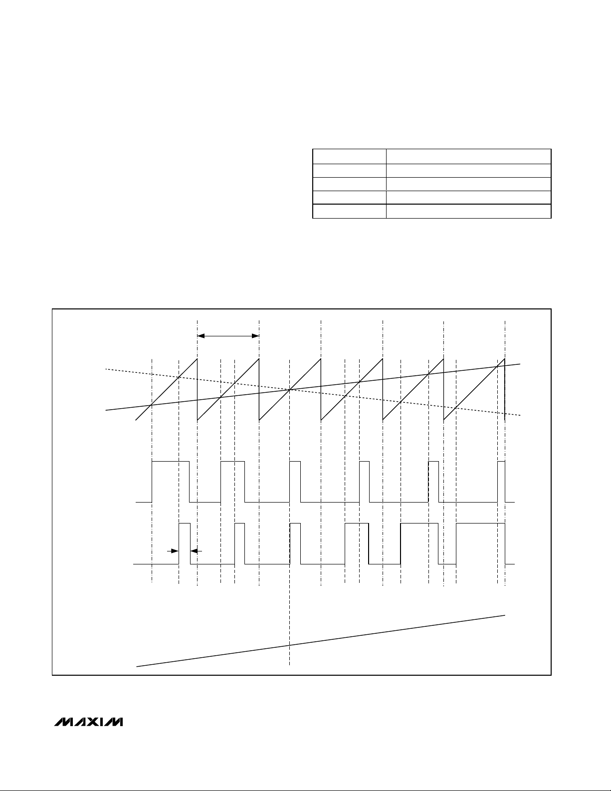
SYNC INPUT MODE
GND FFPWM with fS = 1100kHz
FLOAT FFPWM with fS = 1450kHz
V
DD
SSPWM with fS = 1220kHz ±120kHz
Clocked
FFPWM with fS = external clock frequency
Table 1. Operating Modes
Page 12

fundamental switching frequency and its associated
harmonics (see the Wideband FFT graph in the Typical
Operating Characteristics). The MAX9770 allows the
switching frequency to be changed by +32% should
the frequency of one or more harmonics fall in a sensitive band. This can be done during operation and does
not affect audio reproduction.
Spread-Spectrum Modulation (SSM) Mode
The MAX9770 features a unique, patented spreadspectrum mode that flattens the wideband spectral
components, improving EMI emissions radiated by the
speaker and cables by 5dB. Proprietary techniques
ensure that the cycle-to-cycle variation of the switching
period does not degrade audio reproduction or efficiency (see the Typical Operating Characteristics).
Select SSM mode by setting SYNC = VDD. In SSM
mode, the switching frequency varies randomly by
±120kHz around the center frequency (1.22MHz). The
modulation scheme remains the same, but the period
of the sawtooth waveform changes from cycle-to-cycle
(Figure 2). Instead of a large amount of spectral energy
present at multiples of the switching frequency, the
energy is now spread over a bandwidth that increases
with frequency. Above a few MHz, the wideband spectrum looks like white noise for EMI purposes (Figure 3).
MAX9770
1.2W Low-EMI, Filterless, Mono Class D Amplifier
with Stereo Dir ectDrive Headphone Amplifiers
12 ______________________________________________________________________________________
V
OUT+
- V
OUT-
t
SW
t
SW
t
SW
t
SW
V
IN-
V
IN+
OUT+
OUT-
t
ON(MIN)
Figure 2. MAX9770 Output with an Input Signal Applied (SSM mode)
Page 13

External Clock Mode
The SYNC input allows the MAX9770 to be synchronized to a system clock (allowing a fully synchronous
system), or allocating the spectral components of the
switching harmonics to insensitive frequency bands.
Applying an external clock of 800kHz to 2MHz to SYNC
synchronizes the switching frequency of both the Class
D and charge pump. The period of the SYNC clock can
be randomized, enabling the MAX9770 to be synchronized to another spread-spectrum Class D amplifier
operating in SSM mode.
Filterless Modulation/Common-Mode Idle
The MAX9770 uses Maxim’s unique, patented modulation
scheme that eliminates the LC filter required by traditional
Class D amplifiers, improving efficiency, reducing component count, conserving board space and system cost.
Conventional Class D amplifiers output a 50% duty cycle
square wave when no signal is present. With no filter, the
square wave appears across the load as a DC voltage,
resulting in finite load current, increasing power consumption. When no signal is present at the device input,
the outputs switch as shown in Figure 4. Because the
MAX9770 drives the speaker differentially, the two outputs cancel each other, resulting in no net idle mode voltage across the speaker, minimizing power consumption.
Efficiency
Efficiency of a Class D amplifier is attributed to the
region of operation of the output stage transistors. In a
Class D amplifier, the output transistors act as currentsteering switches and consume negligible additional
power. Any power loss associated with the Class D output stage is mostly due to the I*R loss of the MOSFET
on-resistance, and quiescent current overhead.
MAX9770
1.2W Low-EMI, Filterless, Mono Class D Amplifier
with Stereo Dir ectDrive Headphone Amplifiers
______________________________________________________________________________________ 13
30.0 60.0 80.0 100.0 120.0 140.0 160.0 180.0 280.0 300.0220.0200.0 240.0 260.0
10.0
15.0
20.0
25.0
30.0
35.0
40.0
45.0
50.0
AMPLITUDE (dBµV/m)
FREQUENCY (MHz)
Figure 3. MAX9770 EMI with 75mm of Speaker Cable
VIN = 0V
OUT-
OUT+
V
OUT+
- V
OUT-
= 0V
Figure 4. MAX9770 Output with No Signal Applied
Page 14

The theoretical best efficiency of a linear amplifier is
78%; however, that efficiency is only exhibited at peak
output powers. Under normal operating levels (typical
music reproduction levels), efficiency falls below 30%,
whereas the MAX9770 still exhibits >80% efficiencies
under the same conditions (Figure 5).
DirectDrive
Traditional single-supply headphone drivers have their
outputs biased about a nominal DC voltage (typically
half the supply) for maximum dynamic range. Large
coupling capacitors are needed to block this DC bias
from the headphone. Without these capacitors, a significant amount of DC current flows to the headphone,
resulting in unnecessary power dissipation and possible damage to both headphone and headphone driver.
Maxim’s patented DirectDrive architecture uses a charge
pump to create an internal negative supply voltage. This
allows the headphone outputs of the MAX9770 to be
biased about GND, almost doubling dynamic range
while operating from a single supply. With no DC component, there is no need for the large DC-blocking capacitors. Instead of two large (220µF, typ) tantalum
capacitors, the MAX9770 charge pump requires two
small ceramic capacitors, conserving board space,
reducing cost, and improving the frequency response of
the headphone driver. See the Output Power vs. ChargePump Capacitance and Load Resistance graph in the
Typical Operating Characteristics for details of the possible capacitor sizes. There is a low DC voltage on the driver outputs due to amplifier offset. However, the offset of
the MAX9770 is typically 5mV, which, when combined
with a 32Ω load, results in less than 160µA of DC current
flow to the headphones.
In addition to the cost and size disadvantages of the DCblocking capacitors required by conventional headphone amplifiers, these capacitors limit the amplifier’s
low-frequency response and can distort the audio signal.
Previous attempts at eliminating the output-coupling
capacitors involved biasing the headphone return
(sleeve) to the DC bias voltage of the headphone
amplifiers. This method raises some issues:
1) When combining a microphone and headphone on
a single connector, the microphone bias scheme
typically requires a 0V reference.
2) The sleeve is typically grounded to the chassis.
Using the midrail biasing approach, the sleeve must
be isolated from system ground, complicating product design.
3) During an ESD strike, the driver’s ESD structures are
the only path to system ground. Thus, the driver
must be able to withstand the full ESD strike.
4) When using the headphone jack as a line out to
other equipment, the bias voltage on the sleeve may
conflict with the ground potential from other equipment, resulting in possible damage to the drivers.
Charge Pump
The MAX9770 features a low-noise charge pump. The
switching frequency of the charge pump is 1/2 the
switching frequency of the Class D amplifier, regardless
of the operating mode. When SYNC is driven externally,
the charge pump switches at 1/2 f
SYNC
. When SYNC =
V
DD
, the charge pump switches with a spread-spectrum
pattern. The nominal switching frequency is well beyond
the audio range, and thus does not interfere with the
audio signals, resulting in an SNR of 101dB. The switch
drivers feature a controlled switching speed that minimizes noise generated by turn-on and turn-off transients. By limiting the switching speed of the charge
pump, the di/dt noise caused by the parasitic bond wire
and trace inductance is minimized. Although not typically required, additional high-frequency noise attenuation
can be achieved by increasing the size of C2 (see
Typical Application Circuit). The charge pump is active
in both speaker and headphone modes.
Input Multiplexer/Mixer
The MAX9770 features an input multiplexer/mixer that
allows three different audio sources to be selected/
mixed. Driving a SEL_ input high selects the input channel (see Table 2), and the audio signal is output to the
active amplifier. When a stereo path is selected in
speaker mode (SEL1 or SEL2 = 1), the left and right
MAX9770
1.2W Low-EMI, Filterless, Mono Class D Amplifier
with Stereo Dir ectDrive Headphone Amplifiers
14 ______________________________________________________________________________________
0
30
20
10
50
40
90
80
70
60
100
0 0.1 0.2 0.40.3 0.5 0.6
EFFICIENCY vs. OUTPUT POWER
OUTPUT POWER (W)
EFFICIENCY (%)
MAX9770
CLASS AB
VDD = 3.3V
f = 1kHz
R
L
- 8Ω
Figure 5. MAX9770 Efficiency vs. Class AB Efficiency
Page 15
inputs are attenuated by 6dB and mixed together, resulting in a true mono reproduction of a stereo signal. When
more than one signal path is selected, the sources are
attenuated before mixing to preserve overall amplitude.
Selecting two sources results in 6dB attenuation, selecting three sources results in 9.5dB attenuation.
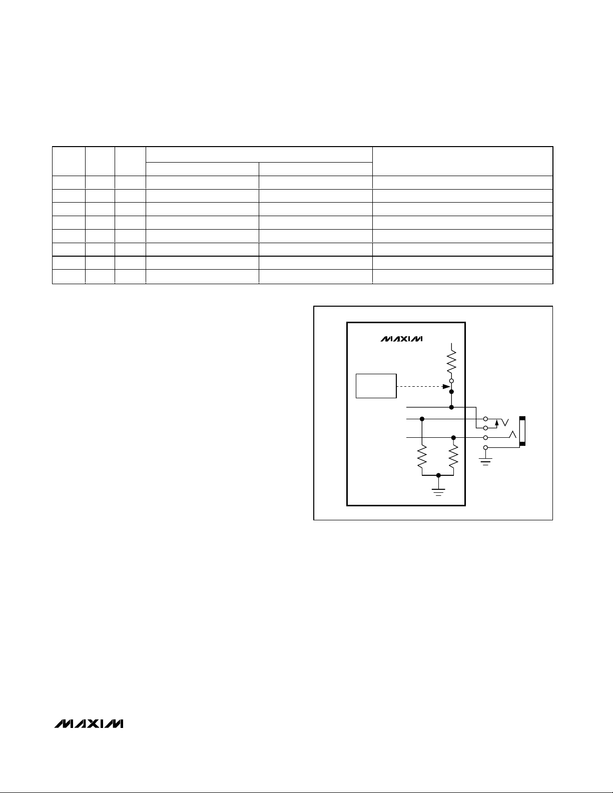
Headphone Sense Input (HPS)
The headphone sense input (HPS) monitors the headphone jack, and automatically configures the device
based upon the voltage applied at HPS. A voltage of
less than 0.8V sets the device to speaker mode. A voltage of greater than 2V disables the bridge amplifiers
and enables the headphone amplifiers.
For automatic headphone detection, connect HPS to
the control pin of a 3-wire headphone jack as shown in
Figure 6. With no headphone present, the output
impedance of the headphone amplifier pulls HPS to
less than 0.8V. When a headphone plug is inserted into
the jack, the control pin is disconnected from the tip
contact and HPS is pulled to V
DD
through the internal
800kΩ pullup. When driving HPS from an external logic
source, ground HPS when the MAX9770 is shut down.
Place a 10kΩ resistor in series with HPS and the headphone jack to ensure ±8kV ESD protection.
Table 2 shows the output amplitude of the selected
channels multiplied by the gain.
BIAS
The MAX9770 features an internally generated, powersupply independent, common-mode bias voltage referenced to GND. BIAS provides both click-and-pop
suppression and sets the DC bias level for the amplifiers.
Choose the value of the bypass capacitor as described
in the BIAS Capacitor section. No external load should
be applied to BIAS. Any load lowers the BIAS voltage,
affecting the overall performance of the device.
Gain Selection
The MAX9770 features a logic-selectable, internally set
gain. GAIN1 and GAIN2 set the gain of the MAX9770
speaker and headphone amplifiers as shown in Table 3.
The MAX9770 can be configured to automatically
switch between two gain settings depending on
whether the device is in speaker or headphone mode.
By driving one or both gain inputs with HPS, the gain of
the device changes when a headphone is inserted or
removed. For example, the block diagram shows HPS
connected to GAIN2, while GAIN1 is connected to VDD.
In this configuration, the gain in speaker mode is 9dB,
while the gain in headphone mode is 1dB. The gain
settings with the HPS connection are shown in Table 4.
MAX9770
1.2W Low-EMI, Filterless, Mono Class D Amplifier
with Stereo Dir ectDrive Headphone Amplifiers
______________________________________________________________________________________ 15
Table 2. Multiplexer/Mixer Settings
HEADPHONE MODE
SEL1
HPOUTL HPOUTR
SPEAKER MODE
0 0 0 MUTE MUTE MUTE
1 0 0 IN1_L IN1_R (IN1_L + IN1_R) / 2
0 1 0 IN2_L IN2_R (IN2_L + IN2_R) / 2
0 0 1 MONO MONO MONO
1 1 0 (IN1_L + IN2_L) / 2 (IN1_R + IN2_R) / 2 (IN1_L + IN1_R + IN2_L + IN2_R) / 4
1 0 1 (IN1_L + MONO) /2 (IN1_R + MONO) / 2 (IN1_L + IN1_R + MONO x 2) / 4
0 1 1 (IN2_L + MONO) / 2 (IN2_R + MONO) / 2 (IN2_L + IN2_R + MONO x 2) / 4
111
( IN1_L + IN1_R + IN2_L + IN2_R + M ON O x 2) / 6
Figure 6. HPS Configuration
SEL2 SELM
( IN 1_L + IN 2_L + M ON O ) / 3 ( IN 1_R + IN 2_R + M ON O ) / 3
MAX9770
800kΩ
SHUTDOWN
CONTROL
HPS
HPOUTL
HPOUTR
10kΩ10kΩ
V
DD
Page 16

MAX9770
Shutdown
The MAX9770 features a 0.1µA, low-power shutdown
mode that reduces quiescent current consumption and
extends battery life. Drive SHDN low to disable the
drive amplifiers, bias circuitry, and charge pump. Bias
is driven to GND and the headphone amplifier output
impedance is 10kΩ in shutdown. Connect SHDN to
VDDfor normal operation.
Click-and-Pop Suppression
Speaker Amplifier
The MAX9770 speaker amplifier features comprehensive
click-and-pop suppression that eliminates audible transients on startup and shutdown. While in shutdown, the
H-bridge is in a high-impedance state. During startup or
power-up, the input amplifiers are muted and an internal
loop sets the modulator bias voltages to the correct levels, preventing clicks and pops when the H-bridge is
subsequently enabled. For 30ms following startup, a
soft-start function gradually unmutes the input amplifiers.
Headphone Amplifier
In conventional single-supply headphone drivers, the
output-coupling capacitor is a major contributor of
audible clicks and pops. Upon startup, the driver
charges the coupling capacitor to its bias voltage, typically half the supply. Likewise, during shutdown, the
capacitor is discharged to GND. This results in a DC
shift across the capacitor, which in turn, appears as an
audible transient at the speaker. Since the MAX9770
headphone amplifier does not require output-coupling
capacitors, this does not arise.
Additionally, the MAX9770 features extensive click-andpop suppression that eliminates any audible transient
sources internal to the device. The Power-Up/PowerDown Waveform in the Typical Operating Characteristics
shows that there are minimal spectral components in the
audible range at the output upon startup or shutdown.
In most applications, the output of the preamplifier driving the MAX9770 has a DC bias of typically half the
supply. During startup, the input-coupling capacitor is
charged to the preamplifier’s DC bias voltage through
the R
F
of the MAX9770, resulting in a DC shift across the
capacitor and an audible click/pop. An internal delay of
50ms eliminates the click/pop caused by the input filter.
Applications Information
Filterless Operation
Traditional Class D amplifiers require an output filter to
recover the audio signal from the amplifier’s output. The
filters add cost, increase the solution size of the amplifier, and can decrease efficiency. The traditional PWM
scheme uses large differential output swings (2 x V
DD
peak-to-peak) at idle and causes large ripple currents.
Any parasitic resistance in the filter components results
in a loss of power, lowering efficiency.
1.2W Low-EMI, Filterless, Mono Class D Amplifier
with Stereo Dir ectDrive Headphone Amplifiers
16 ______________________________________________________________________________________
Table 3. Gain Selection
GAIN1
GAIN2
SPEAKER
GAIN
(dB)
HEADPHONE
GAIN
(dB)
SPEAKER
OUTPUT
POWER
(mW)
SPEAKER
OUTPUT
POWER
(V
IN
= 1V
RMS
)
(mW)
HEADPHONE
OUTPUT
POWER
(mW)
HEADPHONE
OUTPUT
POWER
(VIN = 1V
RMS
)
(mW)
0 0 6 7 500 / 4Ω 500 / 8Ω 60* / 32Ω 60* / 32Ω
0 1 3 4 250 / 4Ω 500 / 4Ω 78 / 16Ω 60* / 32Ω
1 0 9 -2 500 / 8Ω 1000 / 8Ω 19 / 16Ω 39 / 16Ω
1 1 0 1 124 / 4Ω 250 / 4Ω 39 / 16Ω 78 / 16Ω
*Output power limited to 60mW due to output voltage swing.
Table 4. Gain Settings with HPS
Connection
GAIN1 GAIN2
SPEAKER MODE
GAIN
(HPS = 0)
HEADPHONE
MODE GAIN
(HPS = 1)
HPS 0 6 -2
HPS 1 3 1
0 HPS 6 4
1 HPS 9 1
HPS HPS 6 1
00 6 7
01 3 4
10 9 -2
11 0 1
(VIN = 0.707V
RMS
)
(VIN = 0.707V
RMS
)
Page 17

The MAX9770 does not require an output filter. The
device relies on the inherent inductance of the speaker
coil and the natural filtering of both the speaker and the
human ear to recover the audio component of the
square-wave output. Eliminating the output filter results
in a smaller, less costly, and more efficient solution.
Because the frequency of the MAX9770 output is well
beyond the bandwidth of most speakers, voice coil
movement due to the square-wave frequency is minimal. Although this movement is small, a speaker not
designed to handle the additional power may be damaged. For optimum results, use a speaker with a series
inductance >10µH. Typical small 8Ω speakers exhibit
series inductances in the range of 20µH to 100µH.
Output Offset
Unlike Class AB amplifiers, the output offset voltage of a
Class D amplifier does not noticeably increase quiescent
current draw when a load is applied. This is due to the
power conversion of the Class D amplifier. For example, a
15mV DC offset across an 8Ω load results in 1.9mA extra
current consumption in a Class AB device. In the Class D
case, a 15mV offset into 8Ω equates to an additional
power drain of 28µW. Due to the high efficiency of the
Class D amplifier, this represents an additional quiescent
current draw of 28µW/(V
DD
/ 100 x η), which is on the
order of a few microamps.
Power Supplies
The MAX9770 has different supplies for each portion of
the device, allowing for the optimum combination of
headroom and power dissipation and noise immunity.
The speaker amplifiers are powered from PVDD. PV
DD
ranges from 2.5V to 5.5V. The headphone amplifiers
are powered from VDDand SVSS. VDDis the positive
supply of the headphone amplifiers and ranges from
2.5V to 5.5V. SVSSis the negative supply of the headphone amplifiers. Connect SVSSto CPVSS. The charge
pump is powered by CPVDD. CPVDDranges from 2.5V
to 5.5V and should be the same potential as VDD. The
charge pump inverts the voltage at CPVDD, and the
resulting voltage appears at CPVSS. The remainder of
the device is powered by VDD.
Component Selection
Input Filter
The input capacitor (C
IN
), in conjunction with the ampli-
fier input resistance (RIN), forms a highpass filter that
removes the DC bias from an incoming signal (see the
Typical Application Circuit). The AC-coupling capacitor
allows the amplifier to bias the signal to an optimum DC
level. Assuming zero-source impedance, the -3dB point
of the highpass filter is given by:
R
IN
is the amplifier’s internal input resistance value
given in the Electrical Characteristics. Be aware that
the MONO input has a higher input impedance than the
other inputs. Choose CINsuch that f
-3dB
is below the
lowest frequency of interest. Setting f
-3dB
too high
affects the amplifier’s low-frequency response. Setting
f
-3dB
too low can affect the click-and-pop performance.
Use capacitors with low-voltage coefficient dielectrics,
such as tantalum or aluminum electrolytic. Capacitors
with high-voltage coefficients, such as ceramics, may
result in increased distortion at low frequencies.
Output Filter
The MAX9770 speaker amplifier does not require an output filter for normal operation and audio reproduction. The
device passes FCC Class B radiated emissions standards with 100mm of unshielded speaker cables.
However, output filtering can be used if a design is failing
radiated emissions due to board layout or cable length,
or if the circuit is near EMI-sensitive devices. Use a common-mode choke connected in series with the speaker
outputs if board space is limited and emissions are a
concern. Use of an LC filter is necessary if excessive
speaker cable is used.
BIAS Capacitor
BIAS is the output of the internally generated DC bias
voltage. The BIAS bypass capacitor, C
BIAS
improves
PSRR and THD+N by reducing power supply and other
noise sources at the common-mode bias node, and
also generates the clickless/popless, startup/shutdown
DC bias waveforms for the speaker amplifiers. Bypass
BIAS with a 0.047µF capacitor to GND. Large values of
C
BIAS
result in poor click/pop performance, and small-
er values of C
BIAS
result in degradation of PSRR and
increased output noise.
f
RC
dB
IN IN
−
=
3
1
2
π
MAX9770
1.2W Low-EMI, Filterless, Mono Class D Amplifier
with Stereo Dir ectDrive Headphone Amplifiers
______________________________________________________________________________________ 17
Page 18

MAX9770
Charge-Pump Capacitor Selection
Use capacitors with an ESR less than 100mΩ for optimum performance. Low-ESR ceramic capacitors minimize the output resistance of the charge pump. Most
surface-mount ceramic capacitors satisfy the ESR
requirement. For best performance over the extended
temperature range, select capacitors with an X7R
dielectric. Table 5 lists suggested manufacturers.
Flying Capacitor (C1)
The value of the flying capacitor (C1) affects the load
regulation and output resistance of the charge pump. A
C1 value that is too small degrades the device’s ability to
provide sufficient current drive, which leads to a loss of
output voltage. Increasing the value of C1 may improve
load regulation and reduces the charge-pump output
resistance to an extent. Above 1µF, the on-resistance of
the switches and the ESR of C1 and C2 dominate.
Output Capacitor (C2)
The output capacitor value and ESR directly affect the
ripple at CPVSS. Increasing the value of C2 reduces
output ripple. Likewise, decreasing the ESR of C2
reduces both ripple and output resistance. Lower
capacitance values can be used in systems with low
maximum output power levels. See the Output Power
vs. Charge Pump Capacitance and Load Resistance
graph in the Typical Operating Characteristics.
CPVDDBypass Capacitor
The CPVDDbypass capacitor (C3) lowers the output
impedance of the power supply and reduces the
impact of the MAX9770’s charge-pump switching transients. Bypass CPVDDwith C3, the same value as C1,
and place it physically close to the CPVDDand PGND
(refer to the MAX9770 EV kit for a suggested layout).
Layout and Grounding
Proper layout and grounding are essential for optimum
performance. Use large traces for the power-supply
inputs and amplifier outputs to minimize losses due to
parasitic trace resistance, as well as route the head
away from the device. Good grounding improves audio
performance, minimizes crosstalk between channels,
and prevents any switching noise from coupling into
the audio signal. Connect CPGND, PGND, and GND
together at a single point on the PC board. Route
CPGND and all traces that carry switching transients
away from GND, PGND, and the traces and components in the audio signal path.
Connect all components associated with the charge
pump (C2 and C3) to the CPGND plane. Connect SV
SS
and CPVSStogether at the device. Place the chargepump capacitors (C1, C2, and C3) as close to the
device as possible. Bypass VDDand PVDDwith a 1µF
capacitor to GND. Place the bypass capacitors as
close to the device as possible.
Use large, low-resistance output traces. As load impedance decreases, the current drawn from the device outputs increase. At higher current, the resistance of the
output traces decrease the power delivered to the load.
Large output, supply, and GND traces also improve the
power dissipation of the device.
The MAX9770 thin QFN package features an exposed
thermal pad on its underside. This pad lowers the package’s thermal resistance by providing a direct heat conduction path. Due to the high efficiency of the MAX9770’s
Class D amplifier, additional heatsinking is not required. If
additional heatsinking is required, connect the exposed
paddle to GND. See the MAX9770 EV kit data sheet for
suggested component values and layout guidelines.
1.2W Low-EMI, Filterless, Mono Class D Amplifier
with Stereo Dir ectDrive Headphone Amplifiers
18 ______________________________________________________________________________________
Table 5. Suggested Capacitor Manufacturers
SUPPLIER PHONE FAX WEBSITE
Taiyo Yuden 800-348-2496 847-925-0899 www.t-yuden.com
TDK 807-803-6100 847-390-4405 www.component.tdk.com
Page 19
MAX9770
1.2W Low-EMI, Filterless, Mono Class D Amplifier
with Stereo Dir ectDrive Headphone Amplifiers
______________________________________________________________________________________ 19
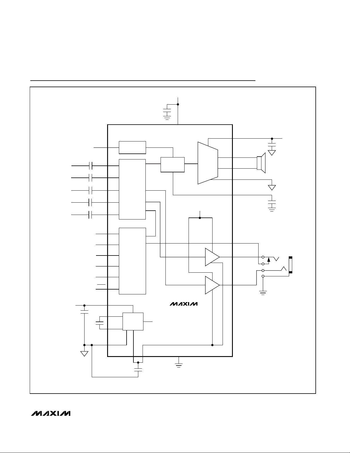
Block Diagram
HPS
IN1_L
GAIN2
HPS
V
DD
V
DD
GND
GND
V
DD
GAIN1
SELM
SEL1
V
DD
CPV
DD
C1P
C1N
CPV
SS
SV
SS
GND
OSC/2
C1
1µF
C
IN
0.47µF
C2
1µF
1µF
CPGND
SYNC
25
(28)
21
(24)
22
(25)
14
(17)
12
(15)
13
(16)
10
(13)
7
(10)
9
(12)
11
(14)
8
(11)5(8)
26
(1)
16
(19)
20
(23)
18
(21)
2
(5)
19
(22)
6
(9)
4
(7)
3
(6)
HPOUTL
HPOUTR
1µF
0.1µF
2.5V TO 5.5V
MIXER/
MUX/GAIN
CONTROL
LEFT-CHANNEL
AUDIO INPUT 1
IN1_R
C
IN
0.47µF
28
(3)
RIGHT-CHANNEL
AUDIO INPUT 1
MONO
C
IN
0.47µF
23
(26)
MONO
AUDIO INPUT
IN2_L
C
IN
0.47µF
24
(27)
LEFT-CHANNEL
AUDIO INPUT 2
IN2_R
C
IN
0.47µF
27
(2)
RIGHT-CHANNEL
AUDIO INPUT 2
CHARGE
PUMP
MUX AND
GAIN CONTROL
HEADPHONE
DETECTION
SHUTDOWN
CONTROL
OSCILLATOR
H-BRIDGE
V
DD
OUT+
PV
DD
2.5V TO 5.5V
V
DD
OUT-
17
(20)
PGND
V
DD
SEL2
15
(18)
SHDN
( ) TSSOP PIN.
C
BIAS
0.047µF
CLASS D
MODULATOR
MAX9770
1
(4)
BIAS
Page 20

MAX9770
1.2W Low-EMI, Filterless, Mono Class D Amplifier
with Stereo Dir ectDrive Headphone Amplifiers
20 ______________________________________________________________________________________
System Diagram
MP3 DAC
MAX9770
IN1_L
2.5V TO 5.5V
2.5V TO 5.5V
IN1_R
1µF
1µF
0.47µF
0.47µF
GND PGND
OUT+
OUT-
HPOUTL
HPS
HPOUTR
V
DD
PV
DD
FM RADIO
MODULE
IN2_L
IN2_R
0.47µF
0.47µF
BASEBAND
PROCESSOR
SHDN
MONO
0.47µF
SEL1
SEL2
SELM
V
DD
GAIN1
V
DD
GAIN2
1µF
0.047µF
BIAS
CPV
SS
CPV
DD
V
SS
CPGND
C1P
C1N
1µF
1µF
Page 21

MAX9770
1.2W Low-EMI, Filterless, Mono Class D Amplifier
with Stereo Dir ectDrive Headphone Amplifiers
______________________________________________________________________________________ 21
Pin Configurations
28
27
26
25
24
23
22
21
20
19
18
17
16
15
1
2
3
4
5
6
7
8
9
10
11
12
13
14
IN1_L
IN2_L
MONO
GAIN1
GAIN2
PV
DD
SEL1
OUTOUT+
PGND
SYNC
SHDN
SELM
SEL2
CPGND
C1P
C1N
CPV
SS
CPV
DD
HPS
SV
SS
HPOUTL
HPOUTR
V
DD
BIAS
IN1_R
IN2_R
GND
TSSOP
TOP VIEW
MAX9770
28
27
26
25
24
23
22
IN1_R
IN2_R
GND
IN1_L
IN2_L
MONO
GAIN1
8
9
10
11
12
13
14
CPV
SS
C1N
C1P
CPGND
SEL1
SEL2
SELM
15
16
17
18
19
20
21
SHDN
SYNC
PGND
OUT+
OUT-
PV
DD
GAIN2
7
6
5
4
3
2
1
CPV
DD
HPS
SV
SS
HPOUTL
HPOUTR
V
DD
BIAS
MAX9770
TQFN
Chip Information
TRANSISTOR COUNT: 7020
PROCESS: BiCMOS
Page 22

MAX9770
1.2W Low-EMI, Filterless, Mono Class D Amplifier
with Stereo Dir ectDrive Headphone Amplifiers
22 ______________________________________________________________________________________
Package Information
(The package drawing(s) in this data sheet may not reflect the most current specifications. For the latest package outline information
go to www.maxim-ic.com/packages
.)
QFN THIN.EPS
D2
(ND-1) X e
e
D
C
PIN # 1
I.D.
(NE-1) X e
E/2
E
0.08 C
0.10 C
A
A1 A3
DETAIL A
0.15
C B
0.15 C A
E2/2
E2
0.10 M C A B
PIN # 1 I.D.
b
0.35x45∞
L
D/2
D2/2
L
C
L
C
e e
L
CC
L
k
k
LL
E
1
2
21-0140
PACKAGE OUTLINE
16, 20, 28, 32, 40L, THIN QFN, 5x5x0.8mm
DETAIL B
L
L1
e
Note: The MAX9770 thin QFN package features an exposed thermal pad on its underside. This pad lowers the package’s thermal resis-
tance by providing a direct heat conduction path. Due to the high efficiency of the MAX9770’s Class D amplifier, additional
heatsinking is not required. The voltage of the exposed paddle is -V
DD
and it is important that the exposed paddle is NOT con-
nected to the ground plane. It should be either left floating or can be tied to the CPV
SS
pin. See the MAX9770 EV kit data sheet for
suggested component values and layout guidelines.
Page 23

MAX9770
1.2W Low-EMI, Filterless, Mono Class D Amplifier
with Stereo Dir ectDrive Headphone Amplifiers
______________________________________________________________________________________ 23
Package Information (continued)
(The package drawing(s) in this data sheet may not reflect the most current specifications. For the latest package outline information
go to www.maxim-ic.com/packages
.)
COMMON DIMENSIONS
3.353.15
T2855-1 3.25 3.353.15 3.25
MAX.
3.20
EXPOSED PAD VARIATIONS
3.00T2055-2 3.10
D2
NOM.MIN.
3.203.00 3.10
MIN.E2NOM. MAX.
NE
ND
PKG.
CODES
1. DIMENSIONING & TOLERANCING CONFORM TO ASME Y14.5M-1994.
2. ALL DIMENSIONS ARE IN MILLIMETERS. ANGLES ARE IN DEGREES.
3. N IS THE TOTAL NUMBER OF TERMINALS.
4. THE TERMINAL #1 IDENTIFIER AND TERMINAL NUMBERING CONVENTION SHALL CONFORM TO JESD 95-1
SPP-012. DETAILS OF TERMINAL #1 IDENTIFIER ARE OPTIONAL, BUT MUST BE LOCATED WITHIN THE
ZONE INDICATED. THE TERMINAL #1 IDENTIFIER MAY BE EITHER A MOLD OR MARKED FEATURE.
5. DIMENSION b APPLIES TO METALLIZED TERMINAL AND IS MEASURED BETWEEN 0.25 mm AND 0.30 mm
FROM TERMINAL TIP.
6. ND AND NE REFER TO THE NUMBER OF TERMINALS ON EACH D AND E SIDE RESPECTIVELY.
7. DEPOPULATION IS POSSIBLE IN A SYMMETRICAL FASHION.
8. COPLANARITY APPLIES TO THE EXPOSED HEAT SINK SLUG AS WELL AS THE TERMINALS.
9. DRAWING CONFORMS TO JEDEC MO220, EXCEPT EXPOSED PAD DIMENSION FOR T2855-1,
T2855-3 AND T2855-6.
NOTES:
SYMBOL
PKG.
N
L1
e
E
D
b
A3
A
A1
k
10. WARPAGE SHALL NOT EXCEED 0.10 mm.
JEDEC
T1655-1
3.203.00 3.10 3.00 3.10 3.20
0.70 0.800.75
4.90
4.90
0.25
0.250--
4
WHHB
4
16
0.350.30
5.10
5.105.00
0.80 BSC.
5.00
0.05
0.20 REF.
0.02
MIN. MAX.NOM.
16L 5x5
3.10
T3255-2
3.00
3.20
3.00 3.10 3.20
2.70
T2855-2 2.60 2.602.80 2.70 2.80
E
2
2
21-0140
PACKAGE OUTLINE
16, 20, 28, 32, 40L, THIN QFN, 5x5x0.8mm
L
0.30 0.500.40
---
---
WHHC
20
5
5
5.00
5.00
0.30
0.55
0.65 BSC.
0.45
0.25
4.90
4.90
0.25
0.65
--
5.10
5.10
0.35
20L 5x5
0.20 REF.
0.75
0.02
NOM.
0
0.70
MIN.
0.05
0.80
MAX.
---
WHHD-1
28
7
7
5.00
5.00
0.25
0.55
0.50 BSC.
0.45
0.25
4.90
4.90
0.20
0.65
--
5.10
5.10
0.30
28L 5x5
0.20 REF.
0.75
0.02
NOM.
0
0.70
MIN.
0.05
0.80
MAX.
---
WHHD-2
32
8
8
5.00
5.00
0.40
0.50 BSC.
0.30
0.25
4.90
4.90
0.50
--
5.10
5.10
32L 5x5
0.20 REF.
0.75
0.02
NOM.
0
0.70
MIN.
0.05
0.80
MAX.
-
40
10
10
5.00
5.00
0.20
0.50
0.40 BSC.
0.40
0.25
4.90
4.90
0.15
0.60
5.10
5.10
0.25
40L 5x5
0.20 REF.
0.75
NOM.
0
0.70
MIN.
0.05
0.80
MAX.
0.20 0.25 0.30
-
0.35 0.45
0.30 0.40 0.50
DOWN
BONDS
ALLOWED
NO
YES3.103.00 3.203.103.00 3.20T2055-3
3.103.00 3.203.103.00 3.20T2055-4
T2855-3 3.15 3.25 3.35 3.15 3.25 3.35
T2855-6 3.15 3.25 3.35 3.15 3.25 3.35
T2855-4 2.60 2.70 2.80 2.60 2.70 2.80
T2855-5 2.60 2.70 2.80 2.60 2.70 2.80
T2855-7 2.60 2.70
2.80
2.60 2.70 2.80
3.20
3.00 3.10T3255-3 3.203.00 3.10
3.203.00 3.10T3255-4 3.203.00 3.10
3.403.20 3.30T4055-1 3.20 3.30 3.40
NO
NO
NO
NO
NO
NO
NO
NO
YES
YES
YES
YES
YES
3.203.00T1655-2 3.10 3.00 3.10 3.20 YE S
Page 24
MAX9770
1.2W Low-EMI, Filterless, Mono Class D Amplifier
with Stereo Dir ectDrive Headphone Amplifiers
Maxim cannot assume responsibility for use of any circuitry other than circuitry entirely embodied in a Maxim product. No circuit patent licenses are
implied. Maxim reserves the right to change the circuitry and specifications without notice at any time.
24 ____________________Maxim Integrated Products, 120 San Gabriel Drive, Sunnyvale, CA 94086 408-737-7600
© 2004 Maxim Integrated Products Printed USA is a registered trademark of Maxim Integrated Products.
Package Information (continued)
(The package drawing(s) in this data sheet may not reflect the most current specifications. For the latest package outline information
go to www.maxim-ic.com/packages
.)
TSSOP4.40mm.EPS
 Loading...