

Page 1
General Description
The MAX975/MAX977 single/dual comparators feature
three different operating modes, and are optimized for
+3V and +5V single-supply applications. The operating
modes are as follows: high speed, high speed with
auto-standby, and low power. Propagation delay is 28ns
in high-speed mode, while supply current is only 250µA.
Supply current is reduced to 3µA in low-power mode.
The auto-standby feature allows the comparator to
automatically change from low-power mode to highspeed mode upon receipt of an input signal. In the
absence of an input signal, the comparator reverts
back to low-power mode after an adjustable timeout
period. The timeout period for the MAX975 to enter
standby is set by a single capacitor. The dual MAX977
features independently adjustable timeout periods for
each comparator using separate capacitors.
The MAX975/MAX977’s inputs have a common-mode
voltage range of -0.2V to (VCC- 1.2V). The differential
input voltage range extends rail to rail. The outputs are
capable of rail-to-rail operation without external pull-up
circuitry, making these devices ideal for interface with
CMOS/TTL logic. All inputs and outputs can tolerate a
continuous short-circuit fault condition to either rail. The
comparator’s internal hysteresis in high-speed mode
ensures clean output switching, even with slow-moving
input signals.
The single MAX975 is available in 8-pin SO and 8-pin
µMAX packages, while the dual MAX977 is available in
14-pin SO and 16-pin QSOP packages.
________________________Applications
Battery-Powered Systems
RF ID Tags
Keyless Entry
Threshold Detectors/Discriminators
3V Systems
IR Receivers
Digital-Line Receivers
____________________________Features
♦ Three Operating Modes:
High Speed
High Speed with Auto-Standby
Low Power
♦ 28ns Propagation Delay (high-speed mode)
♦ 5µA Max Supply Current in Low-Power/
Auto-Standby Modes
♦ +3V/+5V Single-Supply Operation
♦ Rail-to-Rail Outputs
♦ Ground-Sensing Input
♦ Internal Hysteresis (high-speed mode)
♦ Adjustable Timeout Period
♦ µMAX Package (MAX975)
QSOP-16 Package (MAX977)
MAX975/MAX977
Single/Dual, +3V/+5V Dual-Speed
Comparators with Auto-Standby
________________________________________________________________
Maxim Integrated Products
1
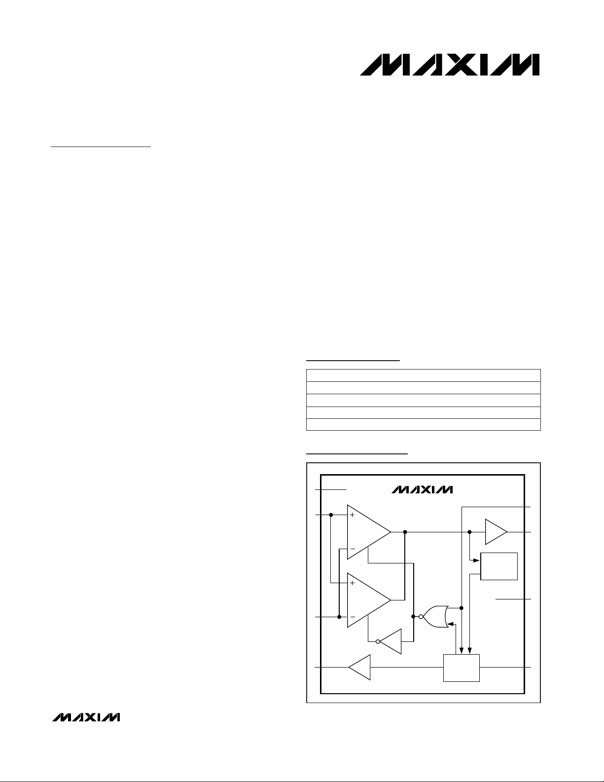
Functional Diagram
19-1141; Rev 1; 11/98
PART
MAX975ESA
MAX975EUA
MAX977ESD
-40°C to +85°C
-40°C to +85°C
-40°C to +85°C
TEMP. RANGE PIN-PACKAGE
8 SO
8 µMAX
14 SO
Ordering Information
Pin Configurations appear at end of data sheet.
MAX977EEE -40°C to +85°C
16 QSOP
MAX975
V
CC
IN+
LP
OUT
GND
STO
HIGH SPEED
LOW POWER
ENABLE
IN-
STAT
TIMING
CIRCUIT
ENABLE
TRANSITION
MONITOR
For free samples & the latest literature: http://www.maxim-ic.com, or phone 1-800-998-8800.
For small orders, phone 1-800-835-8769.
Page 2
MAX975/MAX977
Single/Dual, +3V/+5V Dual-Speed
Comparators with Auto-Standby
2 _______________________________________________________________________________________
ABSOLUTE MAXIMUM RATINGS
ELECTRICAL CHARACTERISTICS
(VCC= +2.7V to +5.25V, specifications are for high-speed mode, TA= -40°C to +85°C, unless otherwise noted. Typical values are at
T
A
= +25°C.) (Note 1)
Stresses beyond those listed under “Absolute Maximum Ratings” may cause permanent damage to the device. These are stress ratings only, and functional
operation of the device at these or any other conditions beyond those indicated in the operational sections of the specifications is not implied. Exposure to
absolute maximum rating conditions for extended periods may affect device reliability.
Supply Voltage (V
CC
)
............................................................+6V
All Other Pins..............................................-0.3V to (V
CC
+ 0.3V)
Duration of Output Short Circuit to GND_ or V
CC
......Continuous
Continuous Power Dissipation (T
A
= +70°C)
8-Pin SO (derate 5.88mW/°C above +70°C)..................471mW
8-Pin µMAX (derate 4.10mW/°C above +70°C).............330mW
14-Pin SO (derate 8.33mW/°C above +70°C)................667mW
16-Pin QSOP (derate 8.33mW/°C above +70°C)...........667mW
Operating Temperature Range ...........................-40°C to +85°C
Storage Temperature Range.............................-65°C to +150°C
Lead Temperature (soldering, 10sec).............................+300°C
250 500
µA
36
I
CC
Supply Current
Per Comparator
35
dB
77
PSRR
Power-Supply
Rejection Ratio
63 90
V2.7 5.25V
CC
Supply-Voltage
Operating Range
UNITSMIN TYP MAXSYMBOLPARAMETER
High-speed mode
µMAX/QSOP
SO
CONDITIONS
Low-power mode
High-speed mode
Auto-standby/low-power modes
VCM= 1V,
2.7V ≤ VCC≤ 5.25V
Common-Mode
Voltage Range
V
CMR
(Note 2) -0.2 VCC- 1.2 V
High-speed mode, TA= +25°C +0.2 ±2
±3High-speed mode, TA= T
MIN
to T
MAX
±1 ±5
Input Offset Voltage
(Note 3)
VCM= 1V,
VCC= 5V
Auto-standby/
low-power modes,
TA= T
MIN
to T
MAX
mV
SO 0.5 2 4
Input-Referred Hysteresis V
HYS
VCM= 1V, VCC= 5V (Note 4)
µMAX/QSOP 0.3 2 4
mV
I
B
SO -100 -300
High-speed mode
µMAX/QSOP -100 -400Input Bias Current
Auto-standby/low-power modes -5
nA
Input Offset Current I
OS
±20 ±100 nA
Input Capacitance C
IN
3 pF
SO 66 90
High-speed mode
µMAX/QSOP 54
Common-Mode
Rejection Ratio
CMRR
-0.2V ≤ V
CM
≤ VCC- 1.2V
Low-power mode 82
dB
SO
V
OS
POWER SUPPLY
COMPARATOR INPUTS
±1 ±7
µMAX/QSOP
Page 3
MAX975/MAX977
Single/Dual, +3V/+5V Dual-Speed
Comparators with Auto-Standby
_______________________________________________________________________________________ 3
ELECTRICAL CHARACTERISTICS (continued)
(VCC= +2.7V to +5.25V, specifications are for high-speed mode, TA= -40°C to +85°C, unless otherwise noted. Typical values are at
T
A
= +25°C.) (Note 1)
C
LOAD
= 10pF,
VCC= 5V
I
SINK
= 2mA, all modes
High-speed mode,
overdrive = 5mV
Low-power mode,
overdrive = 10mV
I
SOURCE
= 2mA, all modes
CONDITIONS
µs0.82 1.6
ns28 50
t
PD+
Propagation Delay, Low to High
(Note 6)
V0.1 0.4V
OL
OUT_ Output Voltage Low
V0.7xVCCVCC/2V
LPIH
LP Input Voltage High
VVCC- 0.4 VCC- 0.1V
OH
OUT_ Output Voltage High
UNITSMIN TYP MAXSYMBOLPARAMETER
VVCC/ 2 0.3xV
CC
V
LPIL
LP Input Voltage Low
µA
(Note 5)
0.01 ±1I
LPB
LP Input Current
µs10t
LP
LP Fall Time
V
CC
= 3V µA0.15I
STO
STO_ Source Current
VVCC/ 2 0.3 x V
CC
V
CIL
STO_ Input Voltage Low
C
LOAD
= 10pF,
VCC= 5V
High-speed mode,
overdrive = 5mV
Low-power mode,
overdrive = 10mV
µs0.48 1.6
ns28 50
t
PD-
Propagation Delay, High to Low
(Note 6)
C
LOAD
= 10pF ns2t
SKEW
Propagation-Delay Skew (Note 6)
MAX977 only, C
LOAD
= 10pF ns1
∆t
PD
Propagation-Delay Matching
C
LOAD
= 10pF,
VCC= 5.0V
High-speed mode
Low-power mode 1.6
ns
1.6
Rise/Fall Time
I
SOURCE
= 3mA, all modes VV
CC
- 0.4V
SH
STAT_ Output Voltage High
I
SINK
= 400µA, all modes V0.4V
SL
STAT_ Output Voltage Low
DIGITAL INPUTS
DIGITAL OUTPUTS
Note 1: The MAX975EUA is 100% production tested at TA= +25°C; all temperature specifications are guaranteed by design.
Note 2: Inferred by CMRR. Either input can be driven to the absolute maximum limit without false output inversion, as long as the
other input is within the specified common-mode input voltage range.
Note 3: V
OS
is defined as the mean of trip points. The trip points are the extremities of the differential input voltage required to make
the comparator output change state (Figure 1).
Note 4: The difference between the upper and lower trip points is equal to the width of the input-referred hysteresis zone (Figure 1).
Note 5: Guaranteed by design. The LP pin is sensitive to noise. If fall times larger than 10µs are expected, bypass LP to ground
using a 0.1µF capacitor.
Note 6: Propagation delay is guaranteed by design. For low-overdrive conditions, V
OS
is added to the overdrive. The following
equation defines propagation-delay skew: t
SKEW
= t
PD+
- t
PD-.
Page 4
MAX975/MAX977
Single/Dual, +3V/+5V Dual-Speed
Comparators with Auto-Standby
4 _______________________________________________________________________________________
ELECTRICAL CHARACTERISTICS (continued)
(VCC= +2.7V to +5.25V, specifications are for high-speed mode, TA= -40°C to +85°C, unless otherwise noted. Typical values are at
T
A
= +25°C.) (Note 1)
CONDITIONS
(Note 9)
10mV overdrive (Note 10)
µs
(Note 8)
3
t
ASB
Auto-Standby Timeout
t
ASBE
UNITSMIN TYP MAXSYMBOLPARAMETER
Auto-Standby Enable Time
µs24t
ASD
Auto-Standby Wake-Up Time
10mV overdrive (Note 11)
(Note 12)
µs1.6t
PWD
Auto-Standby Wake-Up Input
or LP Pulse Width
µs0.8t
ASCD
Auto-Standby Comparator
Disable
(Note 13) µs3t
LPE
Low-Power Enable Time
(Note 14) µs1.1 4t
HSE
High-Speed Enable Time
(Note 15) µs0.7t
LPCD
Low-Power Comparator Disable
(Note 16) ns20t
LPSH
Low-Power STAT_ High
AUTO-STANDBY/LOW-POWER TIMING (Note 7; Figure 2)
Note 7: Timing specifications are guaranteed by design.
Note 8: Set by 1000pF external capacitor at the STO_ pin. t
ASB
is defined as the time from last input transition to STAT_ = high.
Does not include time to go into standby condition (t
ASBE)
.
Note 9: t
ASBE
is defined as the time from when STAT_ goes high to when the supply current drops to 5µA.
Note 10: t
ASD
is defined as the time from the last input transition to when STAT_ goes low. The comparator is in high-speed mode
before STAT_ is low.
Note 11: t
PWD
is defined as the minimum input or LP pulse width to trigger fast-mode operation from auto-standby.
Note 12: t
ASCD
is defined as the time from the last input transition to when the supply current increases to 300µA.
Note 13: t
LPE
is defined as the time from when LP is driven high to when the supply current drops to 5µA.
Note 14: t
HSE
is defined as the time from when LP goes low to when STAT goes low. The comparator is in high-speed mode before
STAT_ is low.
Note 15: t
LPCD
is defined as the time from when LP goes low to when the supply current increases to 300µA.
Note 16: t
LPSH
is defined as the time from when LP goes high to when STAT_ goes high.
ms51016
Page 5
MAX975/MAX977
Single/Dual, +3V/+5V Dual-Speed
Comparators with Auto-Standby
_______________________________________________________________________________________
5
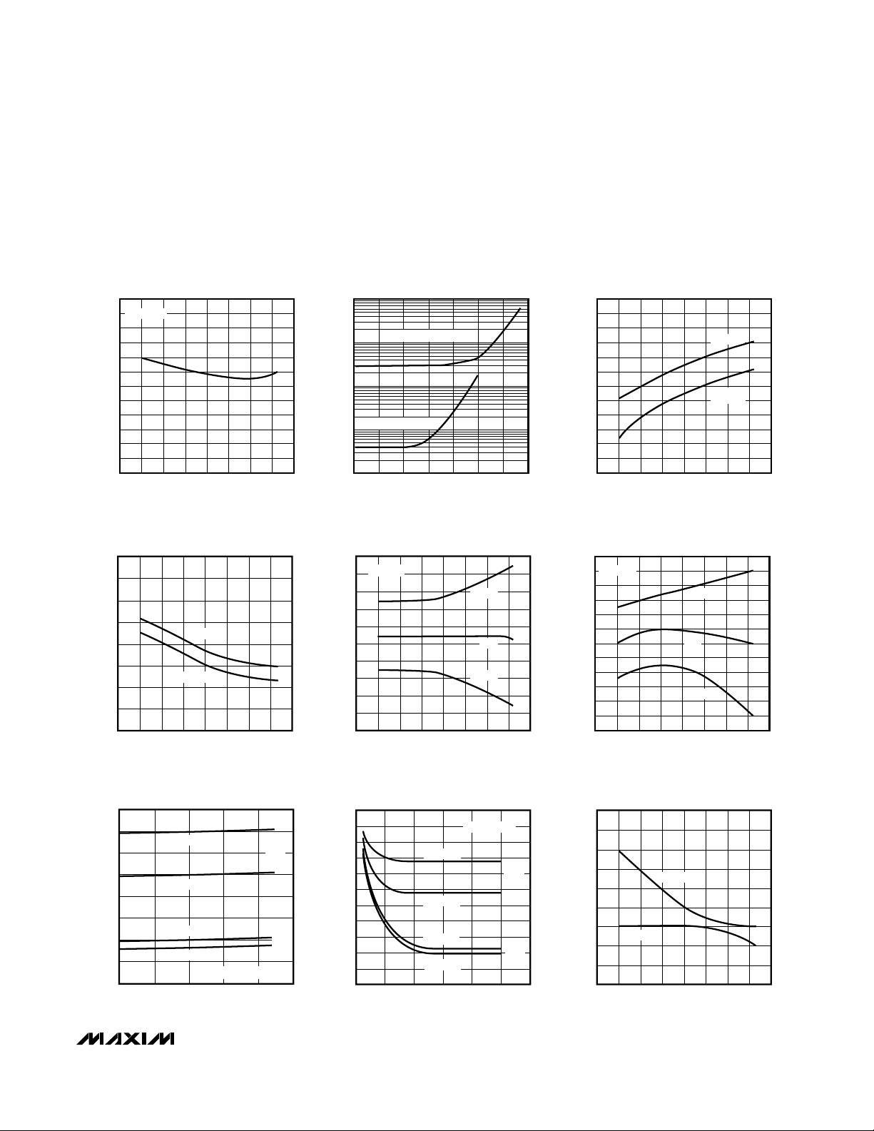
-1.20
-1.15
-1.10
-1.05
-1.00
-0.95
-0.90
-0.85
-0.80
-0.75
-0.70
-0.65
-0.60
-60 -40 -20 0 20 40 60 80 100
LOW-POWER OFFSET VOLTAGE
vs. TEMPERATURE
MAX977-01
TEMPERATURE (°C)
OFFSET VOLTAGE (mV)
VCC = 3V
1
0.01k 10k1k0.1k 100k 1M 10M 100M
SUPPLY CURRENT PER COMPARATOR
vs. OUTPUT TRANSITION FREQUENCY
10
MAX977-02
TRANSITION FREQUENCY (kHz)
SUPPLY CURRENT
PER COMPARATOR (µA)
100
1000
10000
HIGH-SPEED MODE
LOW-POWER MODE
-170
-150
-130
-110
-90
-70
-50
-60 -40 -20 0 20 40 60 80 100
HIGH-SPEED INPUT BIAS CURRENT
vs. TEMPERATURE
MAX977-03
TEMPERATURE (°C)
INPUT BIAS CURRENT (nA)
VCC = 3V
VCC = 5V
7.0
6.5
6.0
5.5
5.0
4.5
4.0
3.0
3.5
-60 -40 -20 0 20 40 60 80 100
LOW-POWER INPUT BIAS CURRENT
vs. TEMPERATURE
MAX977-04
TEMPERATURE (°C)
INPUT BIAS CURRENT (nA)
VCC = 3V
VCC = 5V
200
250
300
350
400
450
500
550
600
0 50 100 150 200 250
LOW-POWER PROPAGATION DELAY
vs. CAPACITIVE LOAD
MAX977-07
CAPACITIVE LOAD (pF)
PROPAGATION DELAY (ns)
VCC = 3V
VCC = 3V
VCC = 5V
VCC = 5V
t
PD-
50mV OVERDRIVE
tPD+
-1.0
-0.8
-0.6
-0.4
-0.2
0
0.2
0.4
0.6
0.8
1.0
-60 -40 -20 0 20 40 60 80 100
HIGH-SPEED VOLTAGE TRIP POINTS/INPUT
OFFSET VOLTAGE vs. TEMPERATURE
MAX977-05
TEMPERATURE (°C)
TRIP POINTS/OFFSET VOLTAGE (mV)
VCC = 5V
V
TRIP+
V
TRIP-
V
OS
-1.2
-1.0
-0.8
-0.6
-0.4
-0.2
0
0.2
0.4
0.6
0.8
1.0
1.2
-60 -40 -20 0 20 40 60 80 100
HIGH-SPEED VOLTAGE TRIP POINTS/INPUT
OFFSET VOLTAGE vs. TEMPERATURE
MAX977-06
TEMPERATURE (°C)
TRIP POINTS/OFFSET VOLTAGE (mV)
V
TRIP-
V
OS
V
TRIP+
VCC = 3V
200
150
250
300
350
400
450
500
550
600
650
700
0 40 80 120 160 240200
LOW-POWER PROPAGATION DELAY
vs. INPUT OVERDRIVE
MAX977-08
INPUT OVERDRIVE (mV)
PROPAGATION DELAY (ns)
VCC = 3V
VCC = 3V
VCC = 5V
VCC = 5V
C
LOAD
=15pF
t
PD-
t
PD+
10.2
10.1
10.0
9.9
9.8
9.7
9.6
9.5
9.4
9.3
-60 -40 -20 0 20 40 60 80 100
AUTO-STANDBY TIMEOUT
vs. TEMPERATURE
MAX977-09
TEMPERATURE (°C)
TIMEOUT (ms)
VCC = 3V
VCC = 5V
__________________________________________Typical Operating Characteristics
(VCC= 3.0V, TA = +25°C, unless otherwise noted.)
Page 6

MAX975/MAX977
Single/Dual, +3V/+5V Dual-Speed
Comparators with Auto-Standby
6 _______________________________________________________________________________________
____________________________Typical Operating Characteristics (continued)
(V
CC
= 3.0V, TA= +25°C, unless otherwise noted.)
100000
1
1 10 100 1000 10000
AUTO-STANDBY TIMEOUT
vs. TIMEOUT CAPACITOR
10
MAX977-10
CAPACITANCE (pF)
TIMEOUT (µs)
100
1000
10000
0.0
0.5
1.0
1.5
2.0
2.5
3.0
3.5
0 5 10 15 20 25 30 35
OUTPUT HIGH VOLTAGE
vs. OUTPUT SOURCE CURRENT
MAX977-11
SOURCE CURRENT (mA)
OUTPUT VOLTAGE (V)
V
CC
= 3V
TA = +85°C
TA = -40°C
TA = +25°C
0.0
0.5
1.0
1.5
2.0
2.5
3.0
3.5
0 5 10 15 20 25 30 35 40
OUTPUT LOW VOLTAGE
vs. OUTPUT SINK CURRENT
MAX977-12
SINK CURRENT (mA)
OUTPUT VOLTAGE (V)
V
CC
= 3V
TA = +85°C
TA = +25°C
TA = -40°C
10
14
18
22
26
30
-60 -40 -20 0 20 40 60 80 100
HIGH-SPEED PROPAGATION DELAY
vs. TEMPERATURE (V
CC
= 5V)
MAX977-13
TEMPERATURE (°C)
PROPAGATION DELAY (ns)
C
LOAD
= 15pF
V
OD
= 50mV
t
PD+
t
PD-
100
120
140
160
180
200
220
240
260
280
300
-60 -40 -20 0 20 40 60 80 100
HIGH-SPEED SUPPLY CURRENT
PER COMPARATOR
vs. TEMPERATURE (V
CC
= 3V)
MAX977-16
TEMPERATURE (°C)
SUPPLY CURRENT (µA)
OUT_ = HIGH
OUT_ = LOW
15
17
19
21
23
25
27
29
31
33
35
-60 -40 -20 0 20 40 60 80 100
HIGH-SPEED PROPAGATION DELAY
vs. TEMPERATURE (V
CC
= 3V)
MAX977-14
TEMPERATURE (°C)
PROPAGATION DELAY (ns)
C
LOAD
= 15pF
t
PD+
t
PD-
VOD = 50mV
100
125
150
175
200
225
250
275
300
325
350
375
400
-60 -40 -20 0 20 40 60 80 100
HIGH-SPEED SUPPLY CURRENT
PER COMPARATOR
vs. TEMPERATURE (V
CC
= 5V)
MAX977-15
TEMPERATURE (°C)
SUPPLY CURRENT (µA)
OUT_ = HIGH
OUT_ = LOW
1.5
2.0
2.5
3.0
3.5
4.0
4.5
-60 -40 -20 0 20 40 60 80 100
STANDBY/LOW-POWER SUPPLY
CURRENT PER COMPARATOR
vs. TEMPERATURE (V
CC
= 5V)
MAX977-17
TEMPERATURE (°C)
SUPPLY CURRENT (µA)
OUT_ = HIGH
OUT_ = LOW
1.8
2.0
2.2
2.4
2.6
2.8
3.0
3.2
3.4
3.6
3.8
-60 -40 -20 0 20 40 60 80 100
STANDBY/LOW POWER-SUPPLY
CURRENT PER COMPARATOR
vs. TEMPERATURE (V
CC
= 3V)
MAX977-18
TEMPERATURE (°C)
SUPPLY CURRENT (µA)
OUT = HIGH
OUT = LOW
Page 7

MAX975/MAX977
Single/Dual, +3V/+5V Dual-Speed
Comparators with Auto-Standby
_______________________________________________________________________________________
7
15.0
17.5
20.0
22.5
25.0
27.5
30.0
32.5
35.0
37.5
40.0
42.5
45.0
0 50 100 150 200 250
HIGH-SPEED PROPAGATION DELAY
vs. CAPACITIVE LOAD
MAX977-19
CAPACITIVE LOAD (pF)
PROPAGATION DELAY (ns)
VCC = +3V
VCC = +5V
t
PD+
t
PD-
t
PD+
t
PD-
C
LOAD
= 15pF
V
OD
= 50mV
0
5
10
15
20
25
30
0 20 40 60 80 100 120 140 160 180 200
HIGH-SPEED PROPAGATION DELAY
vs. INPUT OVERDRIVE
MAX977-20
INPUT OVERDRIVE (mV)
PROPAGATION DELAY (ns)
t
PD-
C
LOAD
= 15pF
VCC = +3V
t
PD+
VCC = +5V
200
240
280
320
360
400
440
480
520
560
600
-60 -40 -20 0 20 40 60 80 100
LOW-POWER PROPAGATION DELAY
vs. TEMPERATURE (V
CC
= 3V)
MAX977-21
TEMPERATURE (°C)
PROPAGATION DELAY (ns)
C
LOAD
= 15pF
V
OD
= 50mV
t
PD+
t
PD-
150
200
250
300
350
400
450
500
550
600
650
700
750
-60 -40 -20 0 20 40 60 80 100
LOW-POWER PROPAGATION DELAY
vs. TEMPERATURE (V
CC
= 5V)
MAX977-22
TEMPERATURE (°C)
PROPAGATION DELAY (ns)
C
LOAD
= 15pF
V
OD
= 50mV
t
PD+
t
PD-
PROPAGATION DELAY tPD+
HIGH-SPEED MODE (V
CC
= +3V)
t
PD+
INPUT
5mV/div
5ns/div
OUTPUT
1V/div
V
OS
V
CC
VCC/2
GND
MAX975/977 TOC23
PROPAGATION DELAY t
PD-
HIGH-SPEED MODE (VCC = +3V)
t
PD-
INPUT
5mV/div
5ns/div
OUTPUT
1V/div
V
OS
V
CC
VCC/2
GND
MAX975/977 TOC24
PROPAGATION DELAY t
PD-
HIGH-SPEED MODE (VCC = +5V)
t
PD-
INPUT
5mV/div
5ns/div
OUTPUT
2V/div
V
OS
V
CC
VCC/2
GND
MAX975/977 TOC25
____________________________Typical Operating Characteristics (continued)
(V
CC
= 3.0V, TA= +25°C, unless otherwise noted.)
Page 8

MAX975/MAX977
Single/Dual, +3V/+5V Dual-Speed
Comparators with Auto-Standby
8 _______________________________________________________________________________________
____________________________Typical Operating Characteristics (continued)
(VCC= 3.0V, TA= +25°C, unless otherwise noted.)
PROPAGATION DELAY t
PD-
LOW-POWER MODE (VCC = +3V)
t
PD-
INPUT
5mV/div
100ns/div
OUTPUT
1V/div
V
OS
V
CC
VCC/2
GND
MAX975/977 TOC27
PROPAGATION DELAY t
PD+
LOW-POWER MODE (VCC = +3V)
t
PD+
INPUT
5mV/div
100ns/div
OUTPUT
1V/div
V
OS
V
CC
VCC/2
GND
MAX975/977 TOC28
PROPAGATION DELAY t
PD+
LOW-POWER MODE (VCC = +5V)
t
PD+
INPUT
5mV/div
100ns/div
OUTPUT
2V/div
V
OS
V
CC
VCC/2
GND
MAX975/977 TOC29
PROPAGATION DELAY t
PD-
LOW-POWER MODE (VCC = +3V)
t
PD-
INPUT
5mV/div
100ns/div
OUTPUT
2V/div
V
OS
V
CC
VCC/2
GND
MAX975/977 TOC30
PROPAGATION DELAY t
PD+
HIGH-SPEED MODE (VCC = +5V)
t
PD+
INPUT
5mV/div
5ns/div
OUTPUT
2V/div
V
OS
V
CC
VCC/2
GND
MAX975/977 TOC26
Page 9

MAX975/MAX977
Single/Dual, +3V/+5V Dual-Speed
Comparators with Auto-Standby
_______________________________________________________________________________________
9
____________________________Typical Operating Characteristics (continued)
(VCC= 3.0V, TA= +25°C, unless otherwise noted.)
10MHz RESPONSE
HIGH-SPEED MODE (V
CC
= +3V)
INPUT
5mV/div
20ns/div
OUTPUT
1V/div
V
OS
V
CC
GND
MAX975/977 TOC33
100kHz RESPONSE
LOW-POWER MODE (V
CC
= +3V)
INPUT
5mV/div
2µs/div
OUTPUT
1V/div
V
OS
V
CC
GND
MAX975/977 TOC31
10MHz RESPONSE
HIGH-SPEED MODE (V
CC
= +5V)
INPUT
5mV/div
20ns/div
OUTPUT
2V/div
V
OS
V
CC
GND
MAX975/977 TOC34
MAX975
AUTO-STANDBY OPERATION
1ms/div
C
STO_
= 100pF
I
np
I
CC
OUT
0µA
250µA
3V
0V
+100mV
-100mV
MAX975/977 TOC35
100kHz RESPONSE
LOW-POWER MODE (V
CC
= +5V)
INPUT
5mV/div
2µs/div
OUTPUT
2V/div
V
OS
V
CC
GND
MAX975/977 TOC32
Page 10

MAX975/MAX977
Single/Dual, +3V/+5V Dual-Speed
Comparators with Auto-Standby
10 ______________________________________________________________________________________
_____________________________________________________________Pin Descriptions
Set Timeout Input. Connect a capacitor from STO to GND to program the time the comparator may
remain idle before entering standby mode. Connect STO to GND to disable the auto-standby feature. Calculate timeout with the following relationship: tASB = 10 x C µs, where C is in pF.
STO5
GroundGND6
Comparator OutputOUT7
LP8
Mode Status Pin. Indicates the operating mode. STAT is high for auto-standby mode or low-power
mode, and during the transition to high-speed mode. STAT = low indicates that the comparator is in
high-speed mode. STAT can source 3mA to power additional circuitry.
STAT4
Inverting Comparator InputIN-3
PIN
Noninverting Comparator InputIN+2
Positive Supply Voltage, +2.7V to +5.25VV
CC
1
FUNCTIONNAME
Low Power Mode Input. Drive LP high for low-power mode. Drive LP low for high-speed mode
(STO = GND) or for high-speed mode with auto-standby. Connect to GND if low-power mode will
not be used. Connect to VCCif high-speed mode will not be used.
FUNCTION
QSOP
1, 9
2, 10
3, 11
4, 5
8, 16
7, 15
6, 14
13
12
NAME
1, 8
STOA,
STOB
Set Idle Timeout Input A/B. Connect a capacitor from STOA/STOB to GND to program
the time in which comparator A/B may remain idle before entering standby mode.
Connect STOA/STOB to GND to disable the auto-standby feature for comparator A/B.
Calculate timeout with the following relationship: t
ASB
= 10 x C µs, where C is in pF.
2, 9
GNDA, GNDB
Ground for Comparator A/B
3, 10
OUTA, OUTB
Output for Comparator A/B
4 V
CC
Positive Supply Voltage, +2.7V to +5.25V. For QSOP, connect pin 4 to pin 5.
7, 14
STATB,
STATA
Mode Status Pin B/A. Indicates the operating mode of comparator B/A.
STATB/STATA is high for auto-standby mode or for low-power mode, and during
the transition to high-speed mode. STATB/STATA = low indicates that comparator
B/A is in high-speed mode. STATB/STATA can source 3mA to power additional
circuitry.
6, 13 INB-, INA- Inverting Input for Comparator B/A
5, 12 INB+, INA+ Noninverting Input for Comparator B/A
11 LP
Low Power Mode Input for both comparators. Drive LP high for low-power mode.
Drive LP low for high-speed mode (STO_ = GND) or for high-speed mode with autostandby. Connect to GND if low-power mode will not be used. Connect to VCCif
high-speed mode will not be used.
— N.C. No connection. Not internally connected.
SO
MAX975
MAX977
Page 11

_______________Detailed Description
The MAX975/MAX977 single/dual comparators have
three operating modes, and use a +2.7V to +5.25V
single supply. The operating modes are as follows:
high speed, high speed with auto-standby, and low
power. Propagation delay is typically 28ns in highspeed mode, while typical supply current is 250µA. In
low-power mode, propagation delay is typically 480ns
and power consumption is only 3µA. The auto-standby
feature switches into low-power standby for each
comparator with unchanging outputs in high-speed
mode. The timeout period, or the time that OUT_
must be idle (unchanged state) for the MAX975/
MAX977 to enter auto-standby, is adjustable by means
of an external capacitor. All inputs and outputs can tolerate a continuous short-circuit fault condition to either
rail. Internal hysteresis in high-speed mode ensures
clean output switching, even with slow-moving input
signals.
The MAX975 functional diagram shows two paralleled
comparators, a timing circuit, a transition detector, and
logic gates. The upper comparator is high speed, while
the lower comparator is a slower low-power comparator. The dual MAX977 features independent timeout
adjustment. The following sections discuss the details
of operation.
Hysteresis (High-Speed Mode Only)
Most high-speed comparators can oscillate in the linear
operating region because of noise or undesired parasitic feedback. This tends to occur when the voltage on
one input is equal to or very close to the voltage on the
other input. The MAX975/MAX977 have internal hysteresis to counter parasitic effects and noise.
The hysteresis in a comparator creates two trip points:
one for the rising input voltage and one for the falling
input voltage (Figure 1). The difference between the trip
points is the hysteresis. When the comparators’ input
voltages are equal, the hysteresis effectively causes
one comparator input voltage to move quickly past the
other, taking the input out of the region where oscillation occurs.
Figure 1 illustrates the case where IN- has a fixed voltage applied and IN+ is varied. If the inputs were
reversed, the figure would be the same, except with an
inverted output.
Auto-Standby Mode
The MAX975/MAX977’s auto-standby function operates
only in high-speed mode. The device enters autostandby when OUT_ remains unchanged for a preprogrammed timeout period. In auto-standby mode, the
low-power comparator is enabled while the high-speed
comparator is disabled and STAT_ goes high. The logic
state and sink/source capabilities of OUT_ remain
unchanged, but propagation delay increases to 480ns.
In this mode, the timing circuitry is powered down, and
the transition detector monitors the low-power comparator for a transition. When an output transition
occurs (OUT_ changes state), the timing circuitry is
MAX975/MAX977
Single/Dual, +3V/+5V Dual-Speed
Comparators with Auto-Standby
______________________________________________________________________________________ 11
INPUTS
LP STO_ IDLE TIME
MODE
STAT
OUTPUT
L t
ASB
= C
STO
x 10µs/pF <t
ASB
High speed
(Auto-standby enabled)
L
L t
ASB
= C
STO
x 10µs/pF ≥t
ASB
Auto-standby H
↓
(falling edge)
L X
High speed
(Auto-standby mode disabled)
L
H X X Low power H
Table 1. Programming
V
OL
V
OH
V
IN-
= 0
V
OS
=
V
TRIP+
+ V
TRIP-
2
COMPARATOR
OUTPUT
V
TRIP+
V
IN+
V
HYST
V
TRIP-
Figure 1. Input and Output Waveforms, Noninverting Input
Varied
Page 12

MAX975/MAX977
powered up, the high-speed comparator is enabled,
the low-power comparator is disabled, and STAT goes
high, placing the MAX975 back into high-speed mode
(Figure 2).
Use an external capacitor, C
STO
, to program the timeout
period required for the comparator to enter autostandby mode. Determine the capacitor required for a
particular timeout period by the relationship t
ASB
=
10 x Cµs, where C is in pF. For example, connecting a
0.1µF capacitor to STO_ results in a timeout period of
1sec. The propagation delay of OUT_ when exiting auto
standby mode is equivalent to the low- power-mode
propagation delay. When STAT_ goes low, the lowpower comparator is disabled and the high-speed comparator is ready for operation. To bring the comparator
out of auto-standby mode without a transition occurring
on OUT_, toggle LP low-high-low. The LP pin is sensitive
to noise. If fall times larger than 10µs are expected,
bypass LP with a 0.1µF capacitor to GND. To disable
auto-standby mode, drive STO_ low or connect it to
ground. Note that driving STO_ low while in autostandby mode will not bring the comparator out of autostandby mode. Also, if driving STO_ with an open drain,
leakage must be less than 1nA. On power-up, the
device is in high-speed mode unless LP is high. The
MAX977 operates in the same manner as the MAX975.
Low-Power Mode
Driving LP high switches the MAX975/MAX977 to lowpower mode. In this mode, the supply current drops to
a maximum of 5µA, and propagation delay increases
typically to 480ns. The high-speed comparator is disabled and the low-power comparator is enabled for
continuous operation. Return to high-speed mode by
driving LP low. The LP pin is sensitive to noise. If fall
times larger than 10µs are expected, bypass LP with a
0.1µF capacitor to GND. The logic state and sink/
source capabilities of OUT_ remain unchanged in lowpower mode.
Input-Stage Circuitry
The MAX975/MAX977 input common-mode range is
from -0.2V to (VCC- 1.2V). But the voltage range for
each comparator input extends to both VCCand GND
rails. The output remains in the correct logic state while
one or both of the inputs are within the common-mode
range. If both input levels are out of the common-mode
range, input-stage current saturation occurs and the
output becomes unpredictable.
Single/Dual, +3V/+5V Dual-Speed
Comparators with Auto-Standby
12 ______________________________________________________________________________________
t
PWD
t
ASB
t
ASD
t
PD-
t
PD+
t
LPSH
t
ASBE
t
LPCD
t
LPE
t
HSE
V
CC
V
OL
V
OH
V
OS
DIFFERENTIAL
INPUT
VOLTAGE
OUT_
STAT_
I
CC (TYP)
LP
0V
300µA
3µA
t
ASCD
V
CC
A
Figure 2. Timing Diagram
Page 13
__________Applications Information
Powering Circuitry with STAT
STAT’s function is to indicate the comparator’s operating mode. When STAT is low, the comparator is in highspeed mode and will meet the guaranteed propagation
delay. When STAT is high, the comparator is in autostandby mode, in low-power mode, or in transition to
high-speed mode. An additional feature of this pin is
that it can source 3mA of current. When STAT is high,
additional circuitry can be powered. This circuitry can
be automatically powered up or powered down,
depending on the input signal or lack of input signal
received by the MAX975/MAX977.
STO_ Considerations
The charge currents for the capacitor connected to
STO_ are on the order of 100nA. This necessitates caution in capacitor type selection and board layout.
Capacitor leakage currents must be less than 1nA to
prevent timing errors. Ceramic capacitors are available
in values up to 1µF, and are an excellent choice for this
application. If a larger capacitance value is needed,
use parallel ceramic capacitors to get the required
capacitance. Aluminum and tantalum electrolytic
capacitors are not recommended due to their higher
leakage currents.
Board layout can create timing errors due to parasitic
effects. Make the STO_ traces as short as possible to
reduce capacitance and coupling effects. When driving
STO_ to disable auto-standby mode, use standard
CMOS logic isolated with a low-leakage (<1nA) diode,
such as National’s FJT1100 (Figure 3). 15nA leakage
typically results in 10% error.
The MAX977 has separate timing inputs (STOA and
STOB). These pins must have separate capacitors. The
timing circuits will not operate correctly if a single
capacitor is used with STOA and STOB connected
together.
The relationship between the timeout period and the
STO_ capacitor is t
ASB
= 10 x C
STO
_ µs, where C
STO
_
is in pF. This equation is for larger capacitance values,
and does not take into account variations due to board
capacitance and board leakage. If less than 1ms is
desired, subtract the ~3pF STO_ parasitic capacitance
from the calculated value.
Circuit Layout and Bypassing
The MAX975/MAX977’shigh gain bandwidth requires
design precautions to realize the comparator’s full highspeed capability. The following precautions are recommended:
1) Use a printed circuit board with an unbroken, lowinductance ground plane.
2) Place a decoupling capacitor (a 0.1µF ceramic
capacitor is a good choice) as close to V
CC
as pos-
sible.
3) Keep lead lengths short on the inputs and outputs, to
avoid unwanted parasitic feedback around the comparators.
4) Solder the devices directly to the printed circuit
board instead of using a socket.
5) Minimize input impedance.
6) For slowly varying inputs, use a small capacitor
(~1000pF) across the inputs to improve stability.
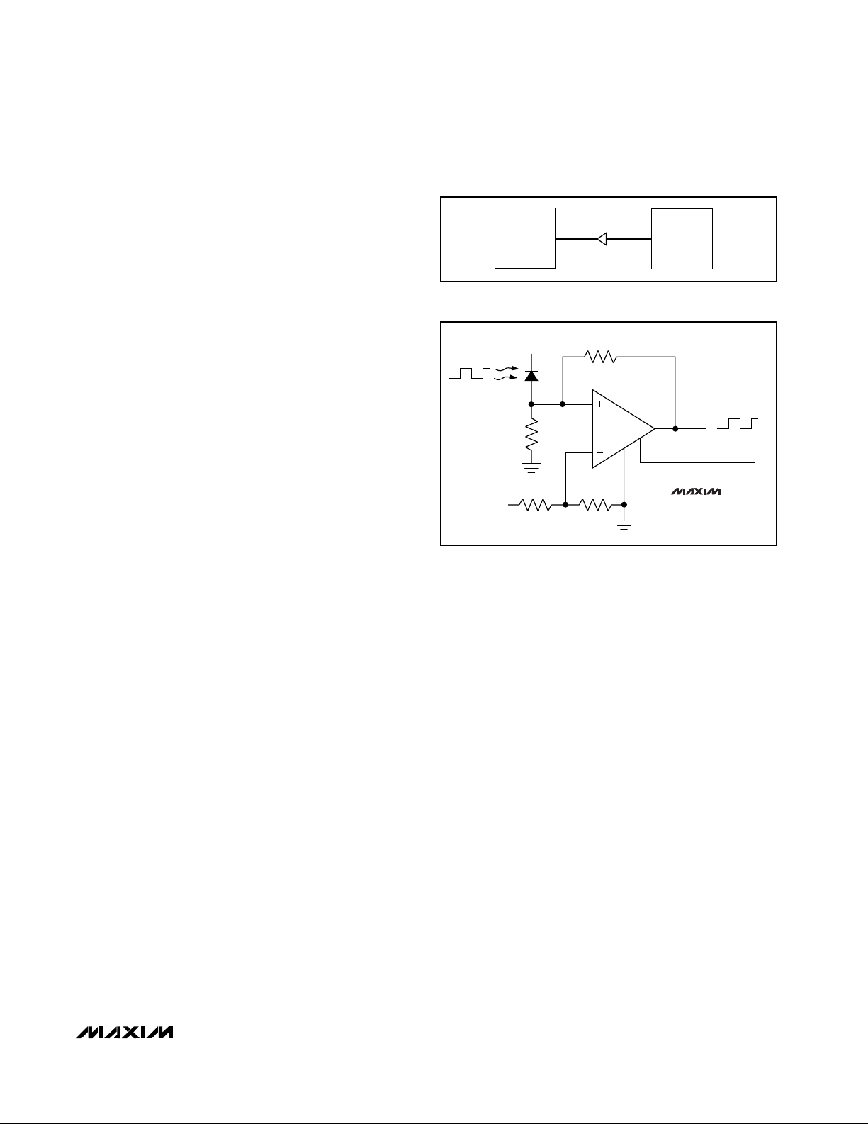
IR Receiver
Figure 4 shows an application using the MAX975 as an
infrared receiver. The infrared photodiode creates a
current relative to the amount of infrared light present.
This current creates a voltage across RD. When this
voltage level crosses the voltage applied by the voltage
divider to the inverting input, the output transitions. If
the photodiode is not receiving enough signal to cause
transitions on the MAX975’s output, STAT is used as a
loss-of-signal indicator. R3 adds additional hysteresis
for noise immunity.
MAX975/MAX977
Single/Dual, +3V/+5V Dual-Speed
Comparators with Auto-Standby
______________________________________________________________________________________ 13
STO_
CMOS
LOGIC
Figure 3. Driving STO_with CMOS Logic
GND
STAT
V
CC
V
CC
V
CC
R
D
R1 R2
R3
OUT
LOSS OF SIGNAL
MAX975
V
CC
Figure 4. IR Receiver
Page 14

MAX975/MAX977
Window Comparator
The MAX977 is ideal for making a window detector
(undervoltage/overvoltage detector). The schematic
shown in Figure 5 uses a MAX6120 reference and component values selected for a 2.0V undervoltage threshold and a 2.5V overvoltage threshold. Choose different
thresholds by changing the values of R1, R2, and R3.
OUTA provides an active-low undervoltage indication,
and OUTB gives an active-low overvoltage indication.
ANDing the two outputs provides an active-high,
power-good signal. The design procedure is as follows:
1) Select R1. The leakage current into INB- is normally
100nA, so the current through R1 should exceed
10µA for the thresholds to be accurate. R1 values in
the 50kΩ to 100kΩ range are typical.
2) Choose the overvoltage threshold (V
OTH
) when V
IN
is rising, and calculate R2 and R3 with the following
formula:
R2 + R3 = R1 x [V
OTH
/ (V
REF
+ VH) - 1]
where VH= 1/2V
HYST
.
3) Choose the undervoltage threshold (V
UTH
) when V
IN
is
falling, and calculate R2 with the following formula:
R2 = (R1 + R2 + R3) x [(V
REF
- VH) / V
UTH
] - R1
where VH= 1/2V
HYST
.
4) Calculate R3 with the following formula:
R3 = (R2 + R3) - R2
5) Verify the resistor values. The equations are as
follows:
V
OTH
= (V
REF
+ VH) x (R1 + R2 + R3) / R1
V
UTH
= (V
REF
- VH) x (R1 + R2 + R3) / (R1 + R2)
Toll-Tag Circuit
The circuit shown in Figure 6 uses a MAX975 in a very
low standby-power AM demodulator circuit that wakes
up a toll tag (part of an automated roadway tollcollection system). This application requires very long
standby times with brief and infrequent interrogations.
In the awake state, it is capable of demodulating the
typical 600kHz AM carrier riding on the 2.4GHz RF signal. In this state, the comparator draws its 250µA highspeed current. After communications have ceased, or
when instructed by the microcontroller, the comparator
returns to its low-power state. The comparator draws
only 3µA in this state, while monitoring for RF activity.
Typically, this application requires two comparators
and a discrete power-management and signalswitchover circuit. The MAX975 circuit is smaller, simpler, less costly, and saves design time.
Single/Dual, +3V/+5V Dual-Speed
Comparators with Auto-Standby
14 ______________________________________________________________________________________
6
1
3
7
10
R3
V
CC
V
CC
V
IN
5
R2
R1
82.1k, 1%
24.9k, 1%
100k, 1%
2
11
9
OVERVOLTAGE
(PIN NUMBERS SHOWN ARE FOR QSOP PACKAGE)
UNDERVOLTAGE
POWER GOOD
C
STOB
1/2
MAX977
MAX6120
14
15
2
V
CC
4
3
1
C
STOA
0.1µF
1/2
MAX977
Figure 5. Window Comparator
I/0
I/0
WAKE-UP IRQ
3V
3V
0.1µF
µP
0.1µF
1M4.7k
GND
STAT
LP
STO
C
STO
V
CC
50Ω
X-BAND
DETECTOR
MAX975
Figure 6. Toll-Tag Reader
Page 15

MAX975/MAX977
Single/Dual, +3V/+5V Dual-Speed
Comparators with Auto-Standby
______________________________________________________________________________________ 15
TRANSISTOR COUNT: 522 (MAX975)
1044 (MAX977)
___________________Chip Information
1
2
3
4
8
7
6
5
LP
OUT
GND
STOSTAT
IN-
IN+
V
CC
MAX975
SO/µMAX
TOP VIEW
14
13
12
11
10
9
8
1
2
3
4
5
6
7
STATA
INAINA+
LPV
CC
OUTA
GNDA
STOA
MAX977
OUTB
GNDB
STOBSTATB
INB-
INB+
SO QSOP
16
15
14
13
12
11
10
9
1
2
3
4
5
6
7
8
STATA
INAINA+
LP
N.C.
OUTB
GNDB
STOB
STOA
GNDA
OUTA
V
CC
V
CC
INB+
INB-
STATB
MAX977
__________________________________________________________Pin Configurations
Page 16

MAX975/MAX977
Single/Dual, +3V/+5V Dual-Speed
Comparators with Auto-Standby
Maxim cannot assume responsibility for use of any circuitry other than circuitry entirely embodied in a Maxim product. No circuit patent licenses are
implied. Maxim reserves the right to change the circuitry and specifications without notice at any time.
16
____________________Maxim Integrated Products, 120 San Gabriel Drive, Sunnyvale, CA 94086 408-737-7600
© 1998 Maxim Integrated Products Printed USA is a registered trademark of Maxim Integrated Products.
________________________________________________________Package Information
8LUMAXD.EPS
QSOP.EPS
 Loading...