

Page 1
General Description
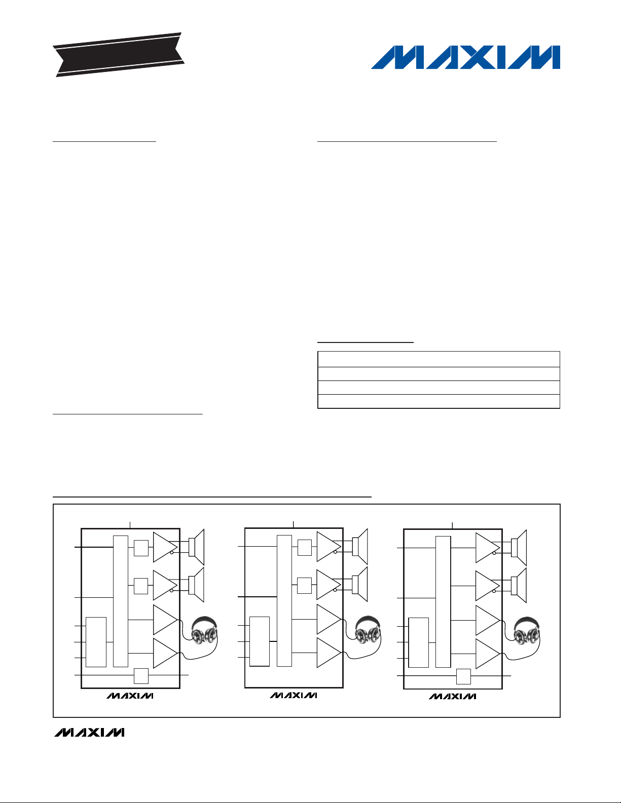
The MAX9756/MAX9757/MAX9758 combine dual, 2.3W,
bridge tied load (BTL) stereo audio power amplifiers and
a DirectDriveTMheadphone amplifier in a single device.
These devices feature single-supply voltage operation,
shutdown mode, logic-selectable gain, a headphone
sense input, a 31-step analog volume control, and industry-leading click-and-pop suppression. The headphone
amplifier uses Maxim’s patent-pending DirectDrive architecture that produces a ground-referenced output from a
single supply, eliminating the need for large DC-blocking
capacitors.
The MAX9756/MAX9757 feature automatic level control
(ALC) that automatically limits output power to the speaker in the event of an overpowered output.
The MAX9756/MAX9758s’ 150mA internal linear regulator provides a complete solution for DAC- or CODECbased designs.
The MAX9756/MAX9757/MAX9758 are offered in spacesaving, thermally efficient 32-pin (5mm x 5mm x 0.8mm)
and 36-pin thin QFN (6mm x 6mm x 0.8mm) packages.
All devices are specified over the extended -40°C to
+85°C temperature range.
Features
♦ Automatic Level Control—Protects Speakers
♦ Analog Volume Control
♦ 120mW DirectDrive Headphone Amplifiers (16Ω)
♦ 150mA Adjustable LDO
♦ Class AB, 2.3W, Stereo BTL Speaker Amplifiers
(3Ω)
♦ High 95dB PSRR
♦ Low-Power Shutdown Mode
♦ Industry-Leading Click-and-Pop Suppression
♦ Short-Circuit and Thermal Protection
♦ Beep Input
MAX9756/MAX9757/MAX9758
2.3W Stereo Speaker Amplifiers and DirectDrive
Headphone Amplifiers with Automatic Level Control
________________________________________________________________ Maxim Integrated Products 1
VOL
ALC
SINGLE SUPPLY 4.5V TO 5.5V
SINGLE SUPPLY 4.5V TO 5.5V SINGLE SUPPLY 4.5V TO 5.5V
1.2V TO 5V
HPS
BEEP
MAX9756
LDO
ALC
VOL
ALC
HPS
BEEP
MAX9757
ALC
VOL
1.2V TO 5V
HPS
BEEP
MAX9758
LDO
Simplified Block Diagrams
Ordering Information
Applications
PART
LDO PIN-PACKAGE
MAX9756ETX+
√√36 Thin QFN-EP**
MAX9757ETJ+*
√ — 32 Thin QFN-EP**
MAX9758ETJ+*
— √ 32 Thin QFN-EP**
19-3782; Rev 0; 8/05
For pricing, delivery, and ordering information, please contact Maxim/Dallas Direct! at
1-888-629-4642, or visit Maxim’s website at www.maxim-ic.com.
EVALUATION KIT
AVAILABLE
Notebook PCs
Tablet PCs
Portable DVD
Players
Flat-Panel TVs
PC Displays
LCD Projectors
Portable Audio
Note: All devices specified for -40°C to +85°C operating
temperature range.
+Denotes lead-free package.
*Future product—contact factory for availability.
**EP = Exposed paddle.
ALC
Page 2
MAX9756/MAX9757/MAX9758
2.3W Stereo Speaker Amplifiers and DirectDrive
Headphone Amplifiers with Automatic Level Control
2 _______________________________________________________________________________________
ABSOLUTE MAXIMUM RATINGS
ELECTRICAL CHARACTERISTICS
(V
DD
= PVDD= HPVDD= CPV
DD
= IN = +5.0V, GND = PGND = CPGND = 0, SHDN = VDD, REGEN = VDD, DR = SET = GND, C
BIAS
= 1µF, C
PVSS
= 1µF, C1 = C2 = 1µF, PREF = unconnected, speaker loads terminated between OUT_+ and OUT_-, headphone load
terminated between HP_ and GND, GAIN1 = GAIN2 = GAIN3 = VOL = 0 (A
V(SP)
= 15dB, A
V(HP)
= 0dB), TA= -40°C to +85°C, unless
otherwise noted. Typical values are at T
A
= +25°C.) (Note 1)
Stresses beyond those listed under “Absolute Maximum Ratings” may cause permanent damage to the device. These are stress ratings only, and functional
operation of the device at these or any other conditions beyond those indicated in the operational sections of the specifications is not implied. Exposure to
absolute maximum rating conditions for extended periods may affect device reliability.
Supply Voltage (VDD, PVDD, HPVDD, CPVDD, IN to GND) ....+6V
PGND, CPGND to GND ......................................................±0.3V
CPVSS, C1N, VSSto GND......................................-6.0V to +0.3V
HP_ to GND ...........................................................................±3V
Any Other Pin .............................................-0.3V to (V
DD
+ 0.3V)
Duration of OUT_ Short Circuit to GND or PVDD........Continuous
Duration of OUT_+ Short Circuit to OUT_- .................Continuous
Duration of HP_ Short Circuit to GND,
VSS, or HPVDD.........................................................Continuous
Duration of OUT Short Circuit to GND........................Continuous
Continuous Current (PVDD, OUT_, PGND) ...........................1.7A
Continuous Current (CPVDD, C1N, CPGND, C1P, CPVSS,
VSS, HPVDD, HP_, IN, OUT).............................................0.85A
Continuous Input Current (all other pins) .........................±20mA
Continuous Power Dissipation (TA= +70°C, single-layer board)
32-Pin Thin QFN (derate 18.6mW/°C above +70°C).....1490mW
36-Pin Thin QFN (derate 20.4mW/°C above +70°C).....1633mW
Continuous Power Dissipation (TA=+70°C, multilayer board)
32-Pin Thin QFN (derate 24.9mW/°C above +70°C).....1990mW
36-Pin Thin QFN (derate 27.7mW/°C above +70°C).....2180mW
Junction Temperature .....................................................+150°C
Operating Temperature Range ...........................-40°C to +85°C
Storage Temperature Range .............................-65°C to +150°C
Lead Temperature (soldering, 10s) .................................+300°C
PARAMETER
SYMBOL
CONDITIONS
MIN
TYP
MAX
UNITS
GENERAL
Supply Voltage Range
Inferred from PSRR test 4.5 5.5 V
Headphone Supply Voltage HPV
DD
Inferred from PSRR test 3.0 5.5 V
HPS = GND, speaker
mode, R
L
= ∞
14 29
Quiescent Supply Current I
DD
IDD = I
VDD
+
HPS = 5V, headphone
mode, R
L
= ∞
713
mA
Shutdown Supply Current I
SHDN
SHDN = REGEN = GND 0.2 5 µA
Bias Voltage V
BIAS
2.2
V
Switching Time t
SW
Gain or input switching 10 µs
Input Resistance R
IN
INL and INR 10 20 30 kΩ
Turn-On Time t
SON
25 ms
SPEAKER AMPLIFIERS (HPS = GND)
Output Offset Voltage V
OS
Measured between OUT_+ and OUT_-,
T
A
= +25°C
mV
PVDD = 4.5V to 5.5V, TA = +25°C 75 95
f = 1kHz, V
RIPPLE
= 200mV
P-P
83
Power-Supply Rejection Ratio
(Note 2)
PSRR
f = 10kHz, V
RIPPLE
= 200mV
P-P
68
dB
RL = 8Ω 0.9 1.3
RL = 4Ω 2.0
Output Power (Note 3) P
OUT
THD+N = 1%, f = 1kHz
(T
A
= +25°C)
R
L
= 3Ω 2.3
W
RL = 8Ω, BTL P
OUT
= 1W, f = 1kHz
Total Harmonic Distortion Plus
Noise
RL = 4Ω, BTL P
OUT
= 1W, f = 1kHz
%
RL = 8Ω, BTL P
OUT
= 1W, BW = 22Hz to
22kHz, unweighted
92
Signal-to-Noise Ratio SNR
R
L
= 8Ω, BTL P
OUT
= 1W, A weighted 95
dB
VDD, PV
DD
I
HPVDD
+ I
CPVDD
THD+N
2.43 2.65
±0.4 ±15
0.009
0.015
Page 3
MAX9756/MAX9757/MAX9758
2.3W Stereo Speaker Amplifiers and DirectDrive
Headphone Amplifiers with Automatic Level Control
_______________________________________________________________________________________ 3
ELECTRICAL CHARACTERISTICS (continued)
(V
DD
= PVDD= HPVDD= CPV
DD
= IN = +5.0V, GND = PGND = CPGND = 0, SHDN = VDD, REGEN = VDD, DR = SET = GND, C
BIAS
= 1µF, C
PVSS
= 1µF, C1 = C2 = 1µF, PREF = unconnected, speaker loads terminated between OUT_+ and OUT_-, headphone load
terminated between HP_ and GND, GAIN1 = GAIN2 = GAIN3 = VOL = 0 (A
V(SP)
= 15dB, A
V(HP)
= 0dB), TA= -40°C to +85°C, unless
otherwise noted. Typical values are at T
A
= +25°C.) (Note 1)
PARAMETER
CONDITIONS
UNITS
Noise V
n
BW = 22Hz to 22kHz, unweighted,
measured at output, input at AC GND
71
µV
RMS
Capacitive-Load Drive C
L
No sustained oscillations
pF
Crosstalk L to R, R to L, f = 10kHz 80 dB
Slew Rate SR Measured between OUT_+ and OUT_- 1.3 V/µs
GAIN3 = 0 GAIN2 = 0 GAIN1 = 0 15
GAIN3 = 0 GAIN2 = 0 GAIN1 = 1
GAIN3 = 0 GAIN2 = 1 GAIN1 = 0 18
GAIN3 = 0 GAIN2 = 1 GAIN1 = 1
GAIN3 = 1 GAIN2 = 0 GAIN1 = 0 21
GAIN3 = 1 GAIN2 = 0 GAIN1 = 1
GAIN3 = 1 GAIN2 = 1 GAIN1 = 0
Gain (Maximum Volume Settings)
(Note 4)
A
VMAX
(SPKR)
GAIN3 = 1 GAIN2 = 1 GAIN1 = 1
dB
Into
shutdown
65
Click-and-Pop Level K
CP
Peak voltage, 32
samples/second,
A weighted (Note 5)
Out of
shutdown
dBV
HEADPHONE AMPLIFIERS (HPS = VDD)
Output Offset Voltage
)
TA = +25°C ±2 ±7 mV
HPVDD = 3V to 5.5V, TA = +25°C 70 90
f = 1kHz, V
RIPPLE
= 200mV
P-P
72
Power-Supply Rejection Ratio
(Note 2)
PSRR
f = 10kHz, V
RIPPLE
= 200mV
P-P
70
dB
RL = 32Ω 40 68
Output Power (Note 3) P
OUT
THD+N = 1%, f = 1kHz
(T
A
= +25°C)
R
L
= 16Ω
mW
RL = 32Ω, V
OUT
= 1V
RMS
, f = 1kHz
Total Harmonic Distortion Plus
Noise
RL = 16Ω, V
OUT
= 1V
RMS
, f = 1kHz
%
RL = 32Ω, BTL P
OUT
= 65mW,
BW = 22Hz to 22kHz, unweighted
97
Signal-to-Noise Ratio SNR
R
L
= 32Ω, BTL P
OUT
= 65W,
BW = 22Hz to 22kHz, A weighted
dB
Noise V
n
BW = 22Hz to 22kHz
µV
RMS
Capacitive-Load Drive C
L
No sustained oscillations
pF
Crosstalk L to R, R to L, f = 10kHz 60 dB
Slew Rate SR 1.4 V/µs
GAIN2 = 0, HPS = 1 0
Gain (Maximum Volume Settings)
(Note 6)
)
GAIN2 = 1, HPS = 1 3.0
dB
Into shutdown 62
Click-and-Pop Level K
CP
Peak voltage, 32
samples/second,
A weighted (Note 4)
50
dBV
SYMBOL
MIN TYP MAX
200
16.5
19.5
22.5
24.0
25.5
38.5
V
OS(HP
THD+N
A
VMAX(HP
130
0.02
0.04
100
20.4
200
Out of shutdown
Page 4
MAX9756/MAX9757/MAX9758
2.3W Stereo Speaker Amplifiers and DirectDrive
Headphone Amplifiers with Automatic Level Control
4 _______________________________________________________________________________________
ELECTRICAL CHARACTERISTICS (continued)
(V
DD
= PVDD= HPVDD= CPV
DD
= IN = +5.0V, GND = PGND = CPGND = 0, SHDN = VDD, REGEN = VDD, DR = SET = GND, C
BIAS
= 1µF, C
PVSS
= 1µF, C1 = C2 = 1µF, PREF = unconnected, speaker loads terminated between OUT_+ and OUT_-, headphone load
terminated between HP_ and GND, GAIN1 = GAIN2 = GAIN3 = VOL = 0 (A
V(SP)
= 15dB, A
V(HP)
= 0dB), TA= -40°C to +85°C, unless
otherwise noted. Typical values are at T
A
= +25°C.) (Note 1)
PARAMETER
CONDITIONS
UNITS
CHARGE PUMP
Charge-Pump Frequency f
OSC
kHz
VOLUME CONTROL
VOL Input Impedance R
VOL
MΩ
VOL Input Hysteresis 10 mV
Full Mute Voltage (Note 7)
0.858 x
V
Full Mute Attenuation fIN = 1kHz -85 dB
Input Impedance R
VOL_
Any gain setting
MΩ
AV = +15dB to 0dB
AV = -2dB to -20dB
Channel Matching
A
V
= -22dB to -56dB
dB
BEEP INPUT
Beep Signal Amplitude Threshold
TA = +25°C, RB = 47kΩ (see BEEP Input
section)
0.3 V
Beep Signal Frequency
Threshold
T
A
= +25°C
Hz
AUTOMATIC LEVEL CONTROL SPEAKER AMPLIFIER (MAX9756/MAX9757)
PREF Threshold Accuracy R
PREF
= 180kΩ 5 8.1 %
Maximum Gain Compression 6.0 6.3 dB
Attack Time CT = 1µF (Note 8) 15 ms
Hold Time Time between attack and release phases 50 ms
0V < VDR < (0.3V x VDD)30
9.5Release Time (Note 9)
C
T
= 1µF,
release from
6dB
0.8V < V
DR
< V
DD
3
s
DR INPUT (TRI-STATE INPUT)
DR Input Voltage High V
DRH
0.8 x
V
DR Input Voltage Middle V
DRM
0.4 x
0.6 x
V
DR Input Voltage Low V
DRL
0
0.3 x
V
Input Leakage Current 0V ≤ VDR ≤ V
DD
±1 µA
LOGIC INPUTS (GAIN_, SHDN, REGEN)
Input High Voltage V
IH
2V
Input Low Voltage V
IL
0.8 V
Input Leakage Current I
IN
±1 µA
SYMBOL
MIN TYP MAX
500 550 600
100
300
V
DD
V
DD
HPV
100
±0.2
±0.3
±1.0
DD
0.4V < VDR < (0.6V x VDD)
V
DD
V
DD
V
DD
Page 5
MAX9756/MAX9757/MAX9758
2.3W Stereo Speaker Amplifiers and DirectDrive
Headphone Amplifiers with Automatic Level Control
_______________________________________________________________________________________ 5
Note 1: All devices are 100% production tested at room temperature. All temperature limits are guaranteed by design.
Note 2: PSRR is specified with the amplifier input connected to GND through R
IN
and CIN.
Note 3: Output power levels are measured with the TQFN’s exposed paddle soldered to the ground plane.
Note 4: Speaker path gain is defined as: A
VSPKR
= (V
OUT+
- V
OUT-
)/V
IN__
).
Note 5: Speaker mode testing performed with 8Ω resistive load connected across BTL output. Headphone mode testing per-
formed with 32Ω resistive load connected between HP_ and GND. Mode transitions are controlled by SHDN.
Note 6: Headphone path gain is defined as: A
VHP
= V
HP_/VIN__
.
Note 7: See Table 3 for detains on the mute levels.
Note 8: Attack envelope is exponential. Attack time is defined as the 15 x 10
3
x CT.
Note 9: Time for the gain to return to within 10% of nominal gain setting after the input signal has fallen below the PREF threshold.
Release is linear in dB. Release time is proportional to magnitude of gain compression.
Note 10: Dropout voltage is defined as (V
IN
- V
OUT
) when V
OUT
is 2% below the value of V
OUT
for VIN= V
OUT(NOM)
+ 1V.
ELECTRICAL CHARACTERISTICS (continued)
(V
DD
= PVDD= HPVDD= CPV
DD
= IN = +5.0V, GND = PGND = CPGND = 0, SHDN = VDD, REGEN = VDD, DR = SET = GND, C
BIAS
= 1µF, C
PVSS
= 1µF, C1 = C2 = 1µF, PREF = unconnected, speaker loads terminated between OUT_+ and OUT_-, headphone load
terminated between HP_ and GND, GAIN1 = GAIN2 = GAIN3 = VOL = 0 (A
V(SP)
= 15dB, A
V(HP)
= 0dB), TA= -40°C to +85°C, unless
otherwise noted. Typical values are at T
A
= +25°C.) (Note 1)
PARAMETER
CONDITIONS
UNITS
LOGIC INPUT HEADPHONE (HPS)
Input High Voltage V
IH
2V
Input Low Voltage V
IL
0.8 V
HPS Pullup Current 35 µA
LOW-DROPOUT LINEAR REGULATOR
Input Voltage Range V
IN
Inferred from line regulation 3.5 5.5 V
I
OUT
= 0mA, SHDN = GND
Supply (Ground) Current I
Q
I
OUT
= 150mA
µA
Shutdown Current I
SHDN
REGEN = 0V 0.1 3 µA
Output Current I
OUT
mA
Fixed Output Voltage Accuracy I
OUT
= 1mA
%
Adjustable Output Voltage Range
V
SET Reference Voltage V
SET
V
SET Dual-Mode Threshold
mV
SET Input Leakage Current I
SET
nA
I
OUT
= 50mA 25 50
Dropout Voltage (Note 10) ΔV
OD
V
OUT
= 4.65V (fixed
output operation)
I
OUT
= 150mA
mV
Output Current Limit I
LIM
mA
Startup Time 20 µs
Line Regulation
V
IN
= 3.5V to 5.5V, V
OUT
= 2.5V,
I
OUT
= 1mA
%/V
Load Regulation V
OUT
= 4.65V, 1mA < I
OUT
< 150mA 0.5 %
f = 1kHz 60
Ripple Rejection V
RIPPLE
= 200mV
P-P
f = 10kHz 50
dB
Output Voltage Noise
20Hz to 22kHz, C
OUT
= 2 x 1µF,
I
OUT
= 150mA, V
OUT
= 4.65V
µV
RMS
SYMBOL
MIN TYP MAX
100 160
350
150
V
SET
1.19 1.21 1.23
200
±20 ±500
100 150
-0.1 +0.01 +0.1
300
100
±1.5
4.85
Page 6
MAX9756/MAX9757/MAX9758
2.3W Stereo Speaker Amplifiers and DirectDrive
Headphone Amplifiers with Automatic Level Control
6 _______________________________________________________________________________________
Typical Operating Characteristics
(VDD= PVDD= HPVDD= CPVDD= IN = +5.0V, GND = PGND = CPGND = 0V, SHDN = VDD, REGEN = DR = SET = GND, C
BIAS
=
1µF, C
PVSS
= 1µF, C1 = C2 = 1µF, PREF = unconnected, GAIN1 = 1, GAIN2 = GAIN3 = VOL = 0V, measurement BW = 22Hz to
22kHz, TA = +25°C, unless otherwise noted.)
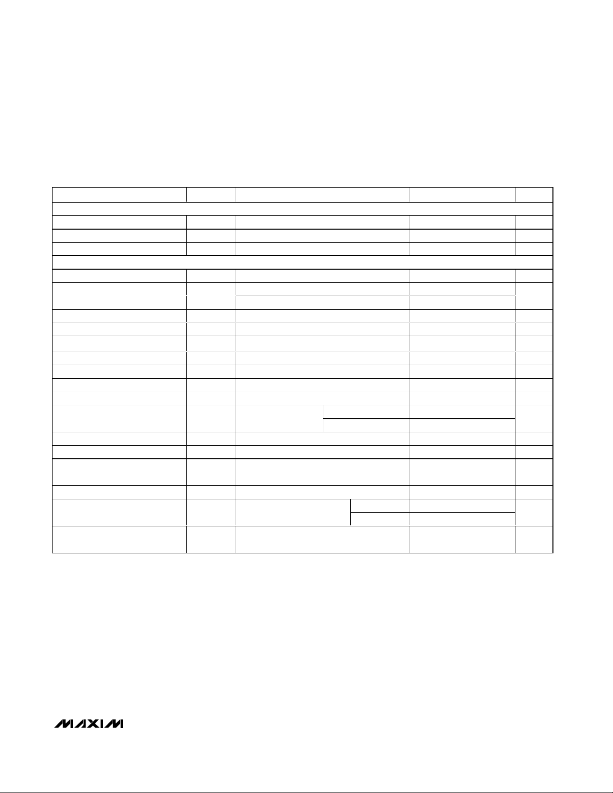
TOTAL HARMONIC DISTORTION PLUS NOISE
vs. FREQUENCY (HEADPHONE MODE)
MAX9756 toc01
FREQUENCY (Hz)
THD+N (%)
10k1k100
0.01
0.1
1
10
0.001
10 100k
VDD = 5V
R
L
= 3
Ω
OUTPUT POWER = 500mW
OUTPUT POWER = 1.8W
TOTAL HARMONIC DISTORTION PLUS NOISE
vs. FREQUENCY (HEADPHONE MODE)
MAX9756 toc02
FREQUENCY (Hz)
THD+N (%)
10k1k100
0.01
0.1
1
10
0.001
10 100k
VDD = 5V
R
L
= 4
Ω
OUTPUT POWER = 500mW
OUTPUT POWER = 1.5W
TOTAL HARMONIC DISTORTION PLUS NOISE
vs. FREQUENCY (HEADPHONE MODE)
MAX9756 toc03
FREQUENCY (Hz)
THD+N (%)
10k1k100
0.01
0.1
1
10
0.001
10 100k
VDD = 5V
R
L
= 8
Ω
OUTPUT POWER = 500mW
OUTPUT POWER = 1W
TOTAL HARMONIC DISTORTION PLUS NOISE
vs. OUTPUT POWER (SPEAKER MODE)
MAX9756 toc04
OUTPUT POWER (W)
THD+N (%)
3.02.52.01.51.00.5
0.01
0.1
1
10
100
0.001
03.5
VDD = 5V
R
L
= 3
Ω
fIN = 100Hz
fIN = 1kHz
fIN = 10kHz
TOTAL HARMONIC DISTORTION PLUS NOISE
vs. OUTPUT POWER (SPEAKER MODE)
MAX9756 toc05
OUTPUT POWER (W)
THD+N (%)
3.02.52.01.51.00.5
0.01
0.1
1
10
100
0.001
0 3.5
VDD = 5V
R
L
= 4
Ω
fIN = 100Hz
fIN = 1kHz
fIN = 10kHz
TOTAL HARMONIC DISTORTION PLUS NOISE
vs. OUTPUT POWER (SPEAKER MODE)
MAX9756 toc06
OUTPUT POWER (W)
THD+N (%)
1.51.00.5
0.01
0.1
1
10
100
0.001
0 2.0
VDD = 5V
R
L
= 8
Ω
fIN = 100Hz
fIN = 1kHz
fIN = 10kHz
OUTPUT POWER
vs. LOAD RESISTANCE (SPEAKER MODE)
MAX9756 toc07
LOAD RESISTANCE (Ω)
OUTPUT POWER (W)
10
0.5
1.0
1.5
2.0
2.5
3.0
0
1100
VDD = 5V
f = 1kHz
THD+N = 10%
THD+N = 1%
POWER DISSIPATION vs. OUTPUT POWER
(SPEAKER MODE)
MAX9756 toc08
OUTPUT POWER (W)
POWER DISSIPATION (W)
3.53.02.52.01.51.00.5
0.5
1.0
1.5
2.0
2.5
3.0
0
0 4.0
f = 1kHz
P
OUT
= P
OUTL
+ P
OUTR
RL = 8
Ω
RL = 4
Ω
POWER-SUPPLY REJECTION RATIO
vs. FREQUENCY (SPEAKER MODE)
MAX9756 toc09
FREQUENCY (Hz)
PSRR (dB)
10k1k100
-110
-100
-90
-80
-70
-60
-50
-40
-30
-20
-10
0
-120
10 100k
V
RIPPLE
= 200mV
P-P
RL = 8
Ω
Page 7
MAX9756/MAX9757/MAX9758
2.3W Stereo Speaker Amplifiers and DirectDrive
Headphone Amplifiers with Automatic Level Control
_______________________________________________________________________________________ 7
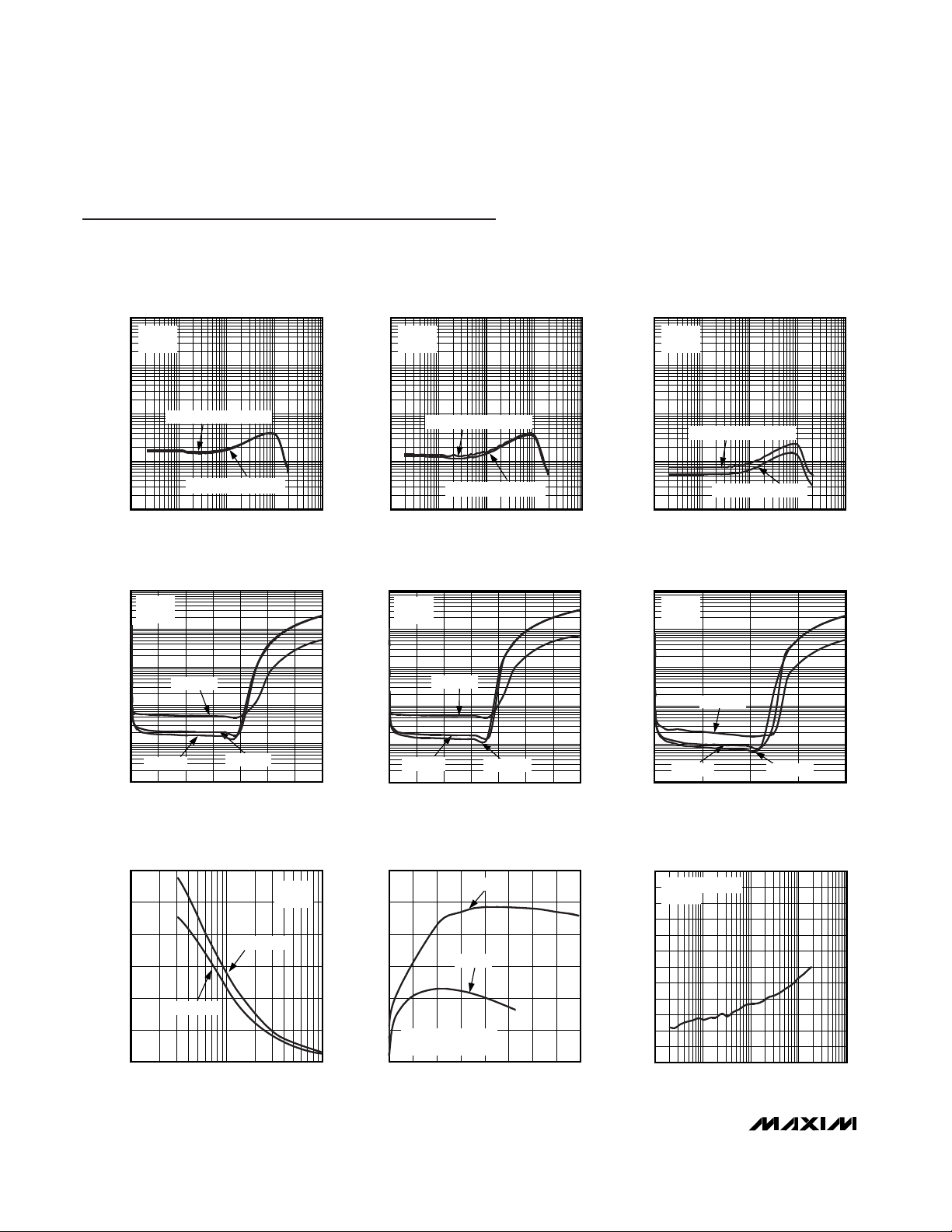
CROSSTALK vs. FREQUENCY
(SPEAKER MODE)
MAX9756 toc10
FREQUENCY (Hz)
CROSSTALK (dB)
10k1k100
-100
-90
-80
-70
-60
-50
-40
-30
-20
-10
0
-110
10 100k
LEFT TO RIGHT
RIGHT TO LEFT
VIN = 200mV
P-P
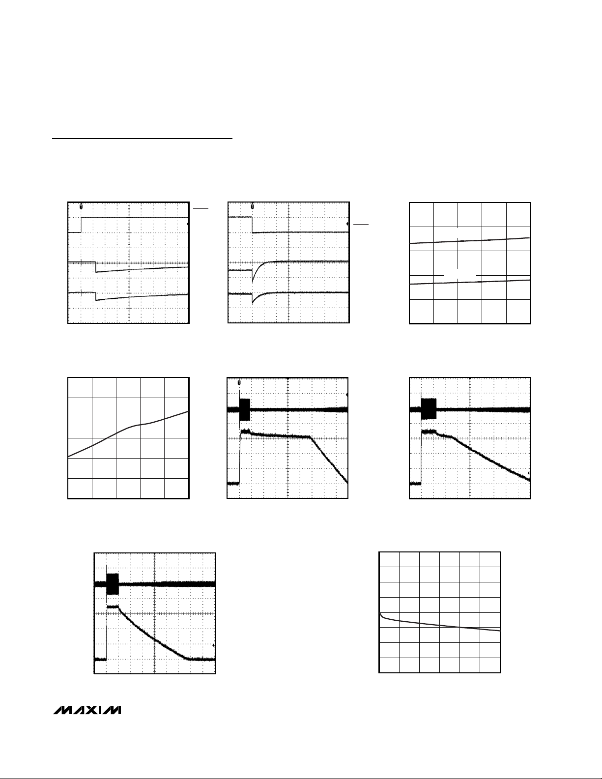
TURN-ON RESPONSE (SPEAKER MODE)
MAX9756 toc11
10ms/div
SHDN
5V/div
OUT_+
2V/div
OUT_2V/div
OUT_+ - OUT_50mV/div
TURN-OFF RESPONSE (SPEAKER MODE)
MAX9756 toc12
10ms/div
SHDN
5V/div
OUT_+
2V/div
OUT_2V/div
OUT_+ - OUT_50mV/div
TOTAL HARMONIC DISTORTION PLUS NOISE
vs. FREQUENCY (HEADPHONE MODE)
MAX9756 toc13
FREQUENCY (Hz)
THD+N (%)
10k1k100
0.01
0.1
1
10
0.001
10 100k
VDD = 5V
R
L
= 16
Ω
OUTPUT POWER = 100mW
OUTPUT POWER = 40mW
TOTAL HARMONIC DISTORTION PLUS NOISE
vs. FREQUENCY (HEADPHONE MODE)
MAX9756 toc14
FREQUENCY (Hz)
THD+N (%)
10k1k100
0.01
0.1
1
10
0.001
10 100k
VDD = 5V
R
L
= 32
Ω
OUTPUT POWER = 20mW
OUTPUT POWER = 60mW
TOTAL HARMONIC DISTORTION PLUS NOISE
vs. FREQUENCY (HEADPHONE MODE)
MAX9756 toc15
FREQUENCY (Hz)
THD+N (%)
10k1k100
0.01
0.1
1
10
0.001
10 100k
VDD = 3.3V
R
L
= 16
Ω
OUTPUT POWER = 80mW
OUTPUT POWER = 20mW
TOTAL HARMONIC DISTORTION PLUS NOISE
vs. FREQUENCY (HEADPHONE MODE)
MAX9756 toc16
FREQUENCY (Hz)
THD+N (%)
10k1k100
0.01
0.1
1
10
0.001
10 100k
VDD = 3.3V
R
L
= 32
Ω
OUTPUT POWER = 50mW
OUTPUT POWER = 20mW
TOTAL HARMONIC DISTORTION PLUS NOISE
vs. OUTPUT POWER (HEADPHONE MODE)
MAX9756 toc17
OUTPUT POWER (mW)
THD+N (%)
18016014012010080604020
0.01
0.1
1
10
100
0.001
0200
HPVDD = 5V
R
L
= 16
Ω
fIN = 100Hz
fIN = 10kHz
fIN = 1kHz
TOTAL HARMONIC DISTORTION PLUS NOISE
vs. OUTPUT POWER (HEADPHONE MODE)
MAX9756 toc18
OUTPUT POWER (mW)
THD+N (%)
908070605040302010
0.01
0.1
1
10
100
0.001
0100
HPVDD = 5V
R
L
= 32
Ω
fIN = 100Hz
fIN = 10kHz
fIN = 1kHz
Typical Operating Characteristics (continued)
(VDD= PVDD= HPVDD= CPVDD= IN = +5.0V, GND = PGND = CPGND = 0V, SHDN = VDD, REGEN = DR = SET = GND, C
BIAS
=
1µF, C
PVSS
= 1µF, C1 = C2 = 1µF, PREF = unconnected, GAIN1 = 1, GAIN2 = GAIN3 = VOL = 0V, measurement BW = 22Hz to
22kHz, TA = +25°C, unless otherwise noted.)
Page 8
MAX9756/MAX9757/MAX9758
2.3W Stereo Speaker Amplifiers and DirectDrive
Headphone Amplifiers with Automatic Level Control
8 _______________________________________________________________________________________
Typical Operating Characteristics (continued)
(VDD= PVDD= HPVDD= CPVDD= IN = +5.0V, GND = PGND = CPGND = 0V, SHDN = VDD, REGEN = DR = SET = GND, C
BIAS
=
1µF, C
PVSS
= 1µF, C1 = C2 = 1µF, PREF = unconnected, GAIN1 = 1, GAIN2 = GAIN3 = VOL = 0V, measurement BW = 22Hz to
22kHz, TA = +25°C, unless otherwise noted.)
TOTAL HARMONIC DISTORTION PLUS NOISE
vs. OUTPUT POWER (HEADPHONE MODE)
MAX9756 toc19
OUTPUT POWER (mW)
THD+N (%)
10080604020
0.01
0.1
1
10
100
0.001
0120
HPVDD = 3.3V
R
L
= 16
Ω
fIN = 100Hz
fIN = 10kHz
fIN = 1kHz
TOTAL HARMONIC DISTORTION PLUS NOISE
vs. OUTPUT POWER (HEADPHONE MODE)
MAX9756 toc20
OUTPUT POWER (mW)
THD+N (%)
80 907040 50 60
301020
0.01
0.1
1
10
100
0.001
0 100
HPVDD = 3.3V
R
L
= 32
Ω
fIN = 100Hz
fIN = 1kHz
fIN = 10kHz
OUTPUT POWER vs. LOAD RESISTANCE
(HEADPHONE MODE)
MAX9756 toc21
LOAD RESISTANCE (Ω)
OUTPUT POWER (mW)
100
20
40
60
80
100
120
140
0
10 1000
HPVDD = 3.3V
f = 1kHz
THD+N = 10%
THD+N = 1%
OUTPUT POWER vs. LOAD RESISTANCE
(HEADPHONE MODE)
MAX9756 toc22
LOAD RESISTANCE (Ω)
OUTPUT POWER (mW)
100
20
40
60
80
100
120
140
160
180
200
0
10 1000
HPVDD = 5V
f = 1kHz
THD+N = 10%
THD+N = 1%
POWER DISSIPATION vs. OUTPUT POWER
(HEADPHONE MODE)
MAX9756 toc23
OUTPUT POWER (mW)
POWER DISSIPATION (mW)
225200175150125100755025
0.2
0.4
0.6
0.8
0
0 250
f = 1kHz
P
OUT
= PHL + P
HR
RL = 16
Ω
RL = 32
Ω
OUTPUT POWER vs. SUPPLY VOLTAGE
(HEADPHONE MODE)
MAX9756 toc24
SUPPLY VOLTAGE (V)
OUTPUT POWER (mW)
5.04.54.03.5
10
20
30
40
50
60
70
80
90
100
110
120
130
140
0
3.0 5.5
RL = 16
Ω
RL = 32
Ω
THD+N = 1%
POWER-SUPPLY REJECTION RATIO
vs. FREQUENCY (HEADPHONE MODE)
MAX9756 toc25
FREQUENCY (Hz)
PSRR (dB)
10k1k100
-90
-80
-70
-60
-50
-40
-30
-20
-10
0
-100
10 100k
V
RIPPLE
= 100mV
P-P
INPUTS AC-GROUNDED
HPVDD = 5V
HPVDD = 3.3V
CROSSTALK vs. FREQUENCY
(HEADPHONE MODE)
MAX9756 toc26
FREQUENCY (Hz)
CROSSTALK (dB)
1010.1
-100
-90
-80
-70
-60
-50
-40
-30
-20
-10
0
-110
0.01 100
RL = 32
Ω
f = 1kHz
V
IN
= 200mV
P-P
RIGHT TO LEFT
LEFT TO RIGHT
OUTPUT POWER vs. CHARGE-PUMP
CAPACITANCE (HEADPHONE MODE)
MAX9756 toc27
LOAD (Ω)
OUTPUT POWER (mW)
3025
20
15
35 40
45
40
30
50
60
70
80
90
100
120
110
130
140
150
20
10 50
C1 = C2 = 1μF
C1 = C2 = 2.2μF
f = 1kHz
THD+N = 1%
Page 9
MAX9756/MAX9757/MAX9758
2.3W Stereo Speaker Amplifiers and DirectDrive
Headphone Amplifiers with Automatic Level Control
_______________________________________________________________________________________ 9
TURN-ON RESPONSE (HEADPHONE MODE)
MAX9756 toc28
10ms/div
SHDN
5V/div
HPR
10mV/div
HPL
10mV/div
TURN-OFF RESPONSE (HEADPHONE MODE)
MAX9756 toc29
10ms/div
SHDN
5V/div
HPR
10mV/div
HPL
10mV/div
SUPPLY CURRENT
vs. SUPPLY VOLTAGE
MAX9756 toc30
SUPPLY VOLTAGE (V)
SUPPLY CURRENT (mA)
5.35.14.94.7
8
11
14
17
20
5
4.5 5.5
HPS = GND
HPS = V
DD
SHUTDOWN CURRENT
vs. SUPPLY VOLTAGE
MAX9756 toc31
SUPPLY VOLTAGE (V)
SHUTDOWN CURRENT (nA)
5.35.14.7 4.9
100
200
300
400
500
600
0
4.5 5.5
POWER LIMITING OF SINE BURST
(FAST ATTACK AND FAST RELEASE)
MAX9756 toc32
10ms/div
OUTPUT
2V/div
CT
1V/div
POWER LIMITING OF SINE BURST
(FAST ATTACK AND SLOW RELEASE)
MAX9756 toc33
40ms/div
OUTPUT
2V/div
CT
1V/div
POWER LIMITING OF SINE BURST
(SLOW ATTACK AND SLOW RELEASE)
MAX9756 toc33
2s/div
OUTPUT
2V/div
CT
1V/div
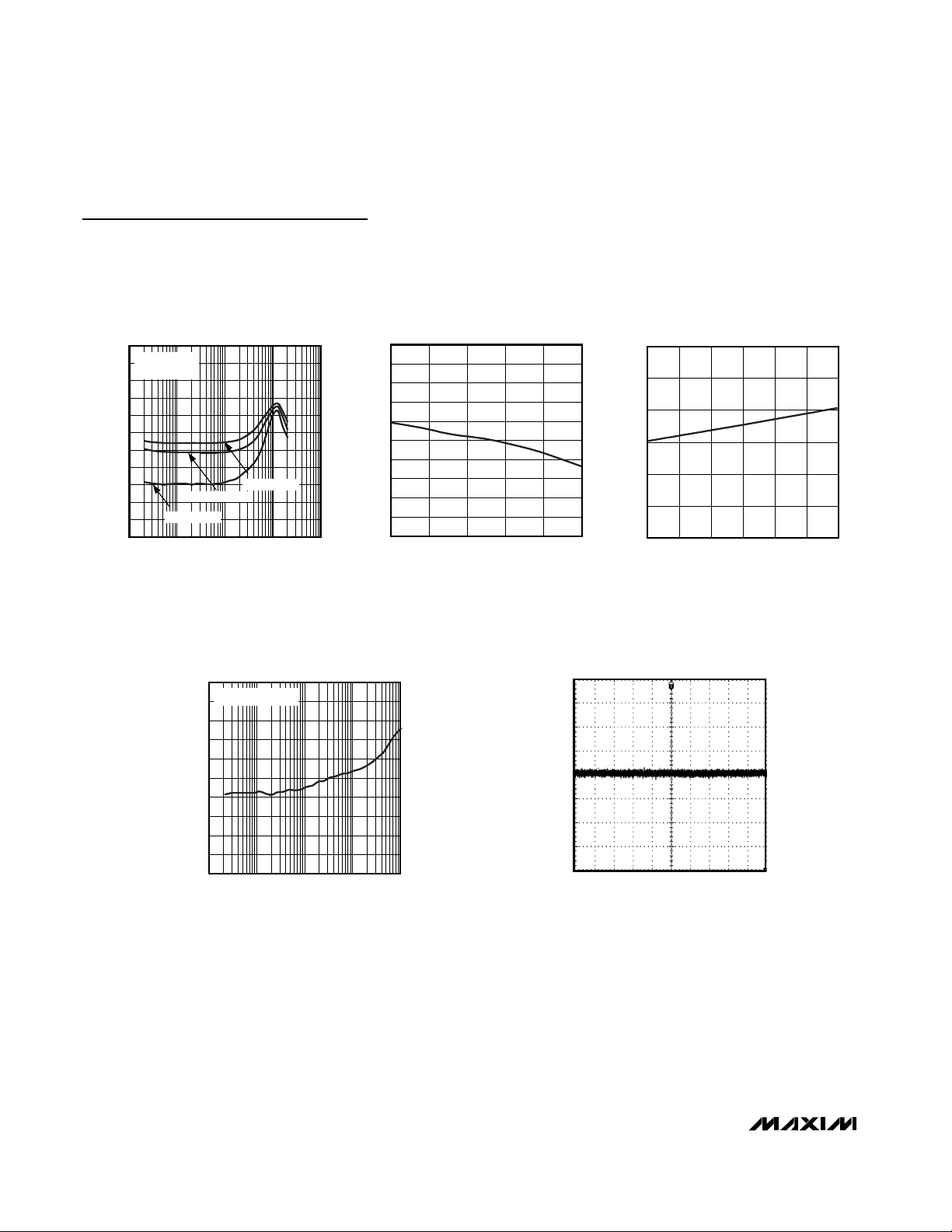
LDO OUTPUT VOLTAGE ACCURACY
vs. LOAD CURRENT
MAX9756 toc35
LOAD CURRENT (mA)
DEVIATION (%)
12510025 50 75
-1.5
-1.0
-0.5
0
0.5
1.0
1.5
2.0
-2.0
0150
Typical Operating Characteristics (continued)
(VDD= PVDD= HPVDD= CPVDD= IN = +5.0V, GND = PGND = CPGND = 0V, SHDN = VDD, REGEN = DR = SET = GND, C
BIAS
=
1µF, C
PVSS
= 1µF, C1 = C2 = 1µF, PREF = unconnected, GAIN1 = 1, GAIN2 = GAIN3 = VOL = 0V, measurement BW = 22Hz to
22kHz, TA = +25°C, unless otherwise noted.)
Page 10
MAX9756/MAX9757/MAX9758
2.3W Stereo Speaker Amplifiers and DirectDrive
Headphone Amplifiers with Automatic Level Control
10 ______________________________________________________________________________________
Typical Operating Characteristics (continued)
(VDD= PVDD= HPVDD= CPVDD= IN = +5.0V, GND = PGND = CPGND = 0V, SHDN = VDD, REGEN = DR = SET = GND, C
BIAS
=
1µF, C
PVSS
= 1µF, C1 = C2 = 1µF, PREF = unconnected, GAIN1 = 1, GAIN2 = GAIN3 = VOL = 0V, measurement BW = 22Hz to
22kHz, TA = +25°C, unless otherwise noted.)
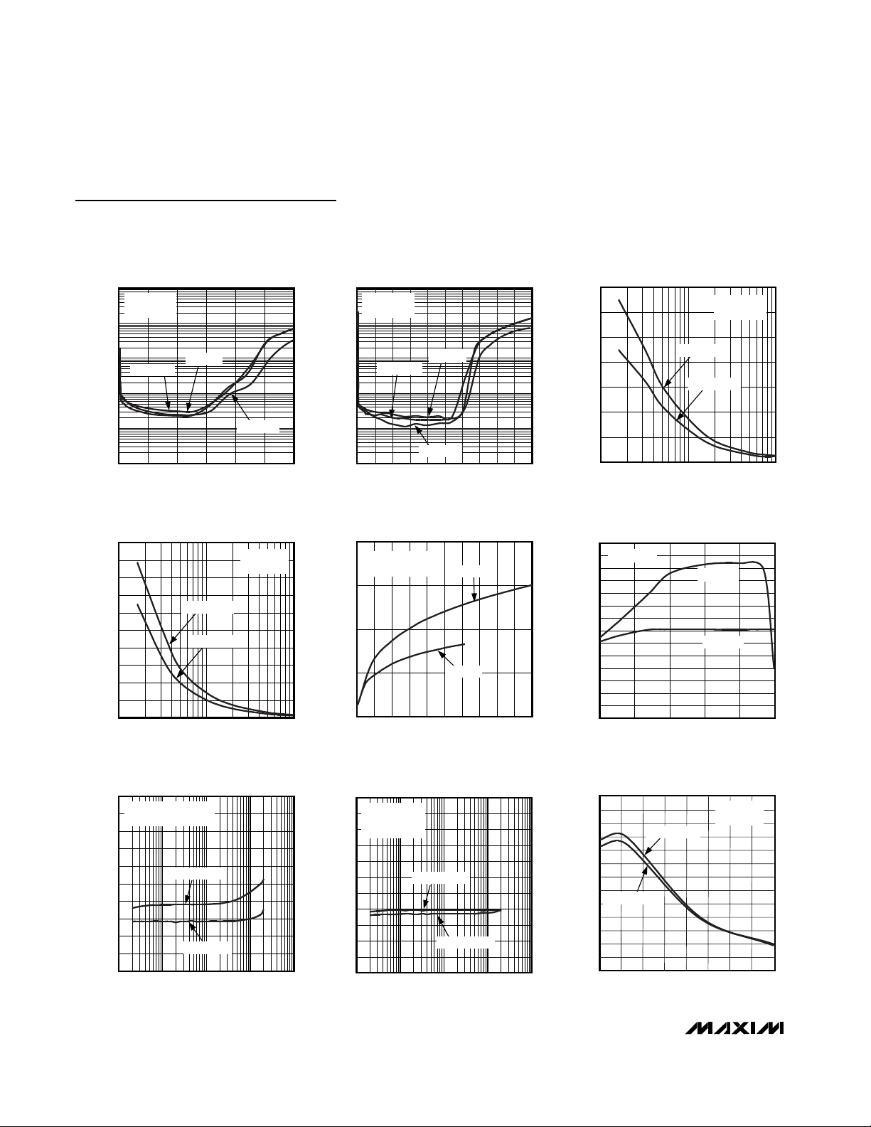
LDO OUTPUT VOLTAGE ACCURACY
vs. TEMPERATURE
MAX7956 toc37
TEMPERATURE (°C)
DEVIATION (%)
603510-15
-4
-3
-2
-1
0
1
2
3
4
5
-5
-40 85
DROPOUT VOLTAGE
vs. LOAD CURRENT
MAX9756 toc38
LOAD CURRENT (mA)
DROPOUT VOLTAGE (V)
125100755025
-200
-100
0
100
200
300
-300
0150
POWER-SUPPLY REJECTION RATIO
vs. FREQUENCY (LDO)
MAX9756 toc39
FREQUENCY (Hz)
PSRR (dB)
10k1k100
-90
-80
-70
-60
-50
-40
-30
-20
-10
0
-100
10 100k
V
RIPPLE
= 100mV
P-P
LDO OUTPUT NOISE
MAX9756 toc40
200μs/div
LDO_OUT
1mV/div
CROSSTALK vs. FREQUENCY
(LDO)
MAX9756 toc36
FREQUENCY (Hz)
CROSSTALK (dB)
1010.1
-100
-90
-80
-70
-60
-50
-40
-30
-20
-10
0
-110
0.01 100
RL = 4
Ω
P
OUT(SPK)
= 1W
I
OUT
= 90mA
I
OUT
= 10mA
I
OUT
= 50mA
Page 11

MAX9756/MAX9757/MAX9758
2.3W Stereo Speaker Amplifiers and DirectDrive
Headphone Amplifiers with Automatic Level Control
______________________________________________________________________________________ 11
Typical Operating Characteristics (continued)
(VDD= PVDD= HPVDD= CPVDD= IN = +5.0V, GND = PGND = CPGND = 0V, SHDN = VDD, REGEN = DR = SET = GND, C
BIAS
=
1µF, C
PVSS
= 1µF, C1 = C2 = 1µF, PREF = unconnected, GAIN1 = 1, GAIN2 = GAIN3 = VOL = 0V, measurement BW = 22Hz to
22kHz, TA = +25°C, unless otherwise noted.)
OUTPUT NOISE
vs. FREQUENCY (LDO)
MAX9756 toc41
FREQUENCY (Hz)
NOISE (μV)
10k1k100
20
30
40
50
60
70
80
90
100
110
10
10 100k
C
OUT
= 2μF
10Hz TO 100kHz
LINE-TRANSIENT RESPONSE
MAX9756 toc42
40μs/div
V
IN
500mV/div
4.5V
5.5V
LDO_OUT
20mV/div
LOAD-TRANSIENT RESPONSE
MAX9756 toc43
20μs/div
50V
0V
I
LOAD
25mV/div
LDO_OUT = 4.65V
20mV/div
LDO SHUTDOWN RESPONSE
MAX9756 toc44
100ms/div
REGEN
5V/div
LDO_OUT
1V/div
Pin Description
PIN
MAX9756
NAME
FUNCTION
1 32 32 INL Left-Channel Audio Input
211
Gain Control Input 1
322
Gain Control Input 2
433
Gain Control Input 3
544
Audible Alert Beep Input
6, 22 5, 21 5, 21
Power Ground
766
Left-Channel Positive Speaker Output
877
Left-Channel Negative Speaker Output
9,19 8,18 8, 18
Speaker Amplifier Power Supply. Bypass with 1µF ceramic capacitor to PGND.
MAX9757 MAX9758
GAIN1
GAIN2
GAIN3
BEEP
PGND
OUTL+
OUTL-
PV
DD
Page 12

MAX9756/MAX9757/MAX9758
2.3W Stereo Speaker Amplifiers and DirectDrive
Headphone Amplifiers with Automatic Level Control
12 ______________________________________________________________________________________
Pin Description (continued)
PIN
MAX9756
FUNCTION
10 9 9
Charge-Pump Power Supply. Bypass with 1µF ceramic capacitor to CPGND.
11 10 10 C1P
Charge-Pump Flying-Capacitor Positive Terminal. Connect a 1µF capacitor from C1P
to C1N.
12 11 11
Charge-Pump Ground
13 12 12 C1N
Charge-Pump Flying-Capacitor Negative Terminal. Connect a 1µF capacitor from
C1P to C1N.
14 13 13
Charge-Pump Negative Output. Connect to VSS.
15 14 14 V
SS
Headphone Amplifier Negative Power Supply. Bypass with 1µF ceramic capacitor to
GND.
16 15 15 HPR Right Headphone Output
17 16 16 HPL Left Headphone Output
18 17 17
Headphone Positive Power Supply. Bypass with 1µF ceramic capacitor to GND.
20 19 19
Right-Channel Negative Speaker Output
21 20 20
Right-Channel Positive Speaker Output
23 22 22 HPS
H ead p hone S ense Inp ut. Leave H P S unconnected i f autom ati c head p hone sensi ng
i s not used .
24 — 23
LD O E nab l e. C onnect RE GE N to V
D D
to enab l e the LD O. C onnect to G N D to
d i sab l e LD O.
25 23 — DR
Automatic Level Control Attack to Release Time Ratio Select. Hardwired to VDD,
GND, or BIAS to set the attack to release ratio; see the ALC section.
26 24 24
Common-Mode Bias Voltage. Bypass with a 1.0µF capacitor to GND.
27 25 25
Shutdown Input. Drive SHDN low to disable the audio amplifiers. Connect SHDN to
V
DD
for normal operation.
28 26 26 VOL Analog Volume Control Input
29 27 —
P ow er - Li m i ti ng Inp ut. C onnect a r esi stor fr om P RE F to G N D to set the sp eaker outp ut
cl am p i ng l evel . Leave P RE F unconnected to d i sab l e ALC ; see the ALC secti on.
30 — 27 SET
Regulator Feedback Input. Connect to GND for 4.65V fixed output. Connect to
resistor-divider for adjustable output; see the Low-Dropout Linear Regulator section.
31 28 28
Ground
32 29 — V
DD
Power Supply
33 — — IN LDO Input. Bypass with two 1µF ceramic capacitors to GND.
34 — 30
LDO Output. Bypass with two 1µF ceramic capacitors to GND.
35 30 — CT
Automatic Level Control Attack and Release Timing Capacitor. Connect CT to GND
to disable ALC; see the ALC section.
36 31 31 INR Right-Channel Audio Input
— — 29 V
DD
Power-Supply and LDO Input. Bypass with two 1µF ceramic capacitors to GND.
EP EP EP EP
Exposed Pad. The external pad lowers the package’s thermal impedance by
providing a direct-heat conduction path from the die to the PC board. Connect the
exposed thermal pad to GND.
MAX9757 MAX9758
NAME
CPV
DD
CPGND
CPV
SS
HPV
DD
OUTR-
OUTR+
REGEN
BIAS
SHDN
PREF
GND
OUT
Page 13

MAX9756/MAX9757/MAX9758
2.3W Stereo Speaker Amplifiers and DirectDrive
Headphone Amplifiers with Automatic Level Control
______________________________________________________________________________________ 13
Detailed Description
The MAX9756/MAX9757/MAX9758 combine dual, 2W
BTL stereo audio power amplifiers with a DirectDrive
headphone amplifier in a single device. The stereo
power amplifiers deliver up to 2.3W per channel into a
3Ω speaker from a 5V supply and the stereo headphone amplifiers deliver up to 130mW per channel into
a 16Ω headphone from a 5V supply.
The MAX9756/MAX9757 feature ALC that automatically
controls output power to the speaker, preventing loudspeaker, overload and provides optimized dynamic
range.
The MAX9756/MAX9757/MAX9758 feature 31-step analog volume control and a BEEP input. The amplifier
gain is pin programmable. These devices feature clickand-pop suppression, eliminating the need for discrete
muting circuitry. Speaker and headphone outputs have
short-circuit and thermal protection.
The MAX9756/MAX9758s’ internal LDO features
Maxim’s Dual Mode™ feedback. The LDO output voltage is either fixed at 4.65V (SET = GND), or adjusted
between 1.23V and 5V using a resistive divider at SET.
The LDO delivers up to 150mA of continuous current,
and can be enabled independently from the audio
amplifiers. Short-circuit and thermal-overload protection are provided for the LDO.
All devices feature a single-supply voltage, a shutdown mode, logic-selectable gain, and a headphone
sense input. Industry-leading click-and-pop suppression eliminates audible transients during power and
shutdown cycles.
Each signal path consists of an input amplifier that sets
the signal-path gain and feeds both the speaker and
headphone amplifiers (Figure 1). The speaker amplifier
uses a BTL architecture, doubling the voltage drive to
the speakers and eliminating the need for DC-blocking
capacitors. The output consists of two signals, identical
in magnitude, but 180° out of phase.
The headphone amplifiers use Maxim’s patented
DirectDrive architecture that eliminates the bulky output
DC-blocking capacitors required by traditional headphone amplifiers. A charge pump inverts the positive
supply (CPVDD), creating a negative supply (CPVSS).
The headphone amplifiers operate from these bipolar
supplies with their outputs biased about GND (Figure 2).
The amplifiers have almost twice the supply range
compared to other single-supply amplifiers, nearly quadrupling the available output power. The benefit of the
GND bias is that the amplifier outputs do not have a DC
component (typically VDD/2). This eliminates the large
DC-blocking capacitors required with conventional
headphone amplifiers, conserving board space and
system cost while improving frequency response.
OUT_+
OUT_-
VOLUME
CONTROL
BIAS
IN_
VOL
BIAS
BIAS
HP_
GND
ALC
Figure 1. MAX9756/MAX9757 Signal Path
+V
DD
-V
DD
GND
CONVENTIONAL DRIVER-BIASING SCHEME
DirectDrive BIASING SCHEME
VDD/2
V
DD
GND
V
OUT
Figure 2. Traditional Headphone Amplifier Output Waveform
vs. DirectDrive Headphone Amplifier Output Waveform
Dual Mode is a trademark of Maxim Integrated Products, Inc.
Page 14

MAX9756/MAX9757/MAX9758
The MAX9756/MAX9757/MAX9758 feature an undervoltage lockout that prevents operation from an insufficient power supply and click-and-pop suppression that
eliminates audible transients on startup and shutdown.
The amplifiers include thermal-overload and short-circuit protection. An additional feature of the amplifiers is
that there is no phase inversion from input to output.
Automatic Level Control (ALC)
Two-watt amplifiers are commonly used in notebook
PCs (almost always powered from a 5V supply). With
an 8Ω speaker driven from a BTL amplifier, the maximum
theoretical continuous power available is:
See Figure 5 for suggested ALC component values.
The ALC feature offers two benefits:
1) To limit amplifier power to protect a loudspeaker.
2) To make input signals with a wide dynamic range
more intelligible by boosting low-level signals without distorting the high-level signals.
A device without ALC experiences clipping at the output
when too much gain is applied to the input. ALC prevents clipping at the output when too much gain is
applied to the input, eliminating output clipping. Figure 3
shows a comparison of an overgained speaker input with
and without ALC.
The MAX9756/MAX9758 control the gain to the speakers
by first detecting that the output voltage to the speaker
has exceeded a preset limit. The speaker amplifier gain
is rapidly reduced to correct for the excessive output
power. This process is known as the attack time. When
the signal subsequently lowers in amplitude, the gain is
held at the reduced state for a short period before slowly
increasing to the normal value. This process is known as
the hold and release time. The speed at which the amplifiers adjust to changing input signals is set by the external timing capacitor C
CT
and the setting of logic input
DR. The output power limit can be set by adjusting the
value of the external resistor connected to PREF. Gain
reduction is a function of input signal amplitude with a
maximum ALC attenuation of 6dB. Figure 4 shows the
effect of an input burst exceeding the preset limit, output
attack, hold and release times.
This process (referred to as “limiting” in audio) limits the
amplifier output power so loudspeaker overload can be
prevented. If the attack and release times are configured
to respond too fast, audible artifacts often, described as
“pumping” or “breathing,” can occur as the gain is rapidly adjusted to follow the dynamics of the signal. For best
results, adjust the time constant of the ALC to accommodate the source material. Notebook applications in which
music CDs and DVDs are the main audio source, a
495µs attack time with a 990ms release time is recommended with a 1.2W output into an 8Ω load.
P
V
R
W
OUT
PEAK
SPEAKER
.=
⎛
⎝
⎜
⎞
⎠
⎟
⎛
⎝
⎜
⎜
⎜
⎜
⎜
⎞
⎠
⎟
⎟
⎟
⎟
⎟
=
⎛
⎝
⎜
⎞
⎠
⎟
⎛
⎝
⎜
⎜
⎜
⎜
⎜
⎞
⎠
⎟
⎟
⎟
⎟
⎟
=
2
5
2
8
156
22
2.3W Stereo Speaker Amplifiers and DirectDrive
Headphone Amplifiers with Automatic Level Control
14 ______________________________________________________________________________________
ALC DISABLE, CLIPPING AT THE OUTPUT
INPUT
SIGNAL
10ms/div
10ms/div
OUTPUT
SIGNAL
ALC ENABLE, NO CLIPPING AT THE OUTPUT
Figure 3. ALC Disabled vs. ALC Enabled
Page 15

Attack Time
The attack time is the time it takes to reduce the gain
after the input signal has exceeded the threshold level.
Suggested attack time range is from 150µs to 50ms.
The gain attenuation in attack is exponential and the
attack time is defined as one time constant. The time
constant of the attack is given by 15,000 x C
CT
sec-
onds (where CCTis the external timing capacitor).
• Use a short attack time for the ALC to react quickly
to transient signals, such as snare drum beats
(music) or gun shots (DVD). Fast attack times can
lead to gain “pumping” where rapid ALC action can
be heard reacting to dynamic material.
• Use a longer attack time to allow the ALC to ignore
short-duration peaks and only reduce the gain when
a noticeable increase in loudness occurs. Short-duration peaks are not reduced, but louder passages are.
This allows the louder passages to be reduced in volume, thereby maximizing output dynamic range.
Having the attack time too long can possibly result in
some damage to the loudspeaker under harsh conditions.
Hold Time
Hold time is the delay after the signal falls below the
threshold level before the release phase is initiated.
Hold time is internally set to 50ms and nonadjustable.
The hold time is cancelled by any signal exceeding the
set threshold level and attack is reinitiated.
Release Time
The release time is how long it takes for the gain to
return to its normal level after the input signal has fallen
below the threshold level and 50ms hold time has
expired. Release time is defined as release from a 6dB
gain compression to 10% of the nominal gain setting
after the input signal has fallen below PREF threshold
and the 50ms hold time has expired. Release time is
adjustable between 95ms and 10s. The release time is
set by picking an attack time using CCTand setting the
attack to release time ratio by configuring DR as shown
in Table 2. Release time is linear in dB with time and is
inversely proportional to the magnitude of gain compression:
• Use a small ratio to maximize the speed of the ALC.
• Use a large ratio to maximize the sound quality and
prevent repeated excursions above the threshold
from being independently adjusted by the ALC.
Release and attack times are set by selecting the
capacitance value between CT and GND, and by setting the logic state of DR (Table 1). DR is a tristate logic
input that sets the attack-to-release time ratio. A fixed
hold time of 50ms is internally added to the release time.
MAX9756/MAX9757/MAX9758
2.3W Stereo Speaker Amplifiers and DirectDrive
Headphone Amplifiers with Automatic Level Control
______________________________________________________________________________________ 15
OUTPUT
2V/div
CT
1V/div
10ms/div
Figure 4. Attack, Hold, and Release Time
Table 1. Attack and Release Time
ATTACK TIME RELEASE TIME
TIMING CAPACITOR
(C
CT
)
DR = ‘X’ DR = V
DD
DR = V
BIAS
DR = GND
10nF 150µs 30ms 95ms 300ms
33nF 495µs 99ms 313ms 990ms
100nF 1.5ms 300ms 950ms 3s
330nF 4.95ms 990ms 3.1s 9.9s
1µF 15ms 3s 9.5s —
2.2µF 33ms 6.6s — —
3.3µF 49.5ms 10s — —
Page 16

MAX9756/MAX9757/MAX9758
The release/attack time ratio that can be achieved by
programming DR is listed in Table 2.
Output Power Threshold
To set the threshold at which speaker output is
clamped, an external resistor must be connected from
PREF to ground. The suggested external resistor range
is from 100kΩ to 200kΩ (for best results use a 1% resistor). Leaving PREF unconnected disables the ALC
function. A constant current of 12µA is sourced at
PREF, so that a 180kΩ resistor results in 1.2W clamp
limit on an 8Ω load and a 200kΩ resistor results in a
1.5W clamp limit on an 8Ω load (Figure 6).
Use the following equation to choose the value for
R
PREF
for the desired maximum output power level
based on a sine wave input:
Gain Selection
The MAX9756/MAX9757/MAX9758 feature an internally
set, selectable gain. The GAIN1, GAIN2, and GAIN3
inputs set the maximum gain for the speaker and headphone amplifiers (Table 3). The gain of the device can
vary based upon the voltage at VOL but does not
exceed the maximum gain listed below (see the Analog
Volume (VOL) Control section).
Rk
PR
PREF
OUT L
=
⎛
⎝
⎜
⎞
⎠
⎟
×
⎛
⎝
⎜
⎞
⎠
⎟
⎛
⎝
⎜
⎜
⎞
⎠
⎟
⎟
180
1 166 8
Ω
.
2.3W Stereo Speaker Amplifiers and DirectDrive
Headphone Amplifiers with Automatic Level Control
16 ______________________________________________________________________________________
MAX9756
MAX9757
33nF
180kΩ
VALUES SHOWN FOR AN OUTPUT POWER THRESHOLD OF 1.2W WITH AN
R
L
= 8Ω ATTACK TIME OF 495μs AND A RELEASE TIME OF 990ms
DR
5V
V
DD
CT
PREF
Figure 5. Recommended Output Power Threshold, Attack, and
Release Time Components
OUTPUT POWER THRESHOLD
vs. R
PREF
R
PREF
(kΩ)
OUTPUT POWER THRESHOLD (W)
190180170160150140130120110
0.5
1.0
1.5
2.0
2.5
3.0
0
100 200
RL = 4Ω
RL = 8Ω
Figure 6. Output Power Threshold vs. R
PREF
Table 2. Release to Attack Ratio
DR RELEASE/ATTACK RATIO
V
DD
200
V
BIAS
633
GND 2000
Table 3. Maximum Gain Settings
GAIN3 GAIN2 GAIN1 SPEAKER MODE GAIN (dB) HEADPHONE MODE GAIN (dB)
0 0 0 +15 0
0 0 1 +16.5 0
0 1 0 +18 +3
0 1 1 +19.5 +3
1 0 0 +21 0
1 0 1 +22.5 0
1 1 0 +24 +3
1 1 1 +25.5 +3
Page 17

Analog Volume Control (VOL)
The MAX9756/MAX9757/MAX9758 feature an analog
volume control that varies the gain of the device in 31
discrete steps based upon the DC voltage applied to
VOL (see Table 4). The input range of VOL is from 0
(full volume) to HPVDD(full mute), with example step
sizes shown in Table 3. Connect the reference of the
device driving VOL (Figure 7) to HPVDD. Connect VOL
to GND (full volume) if volume control is not used.
MAX9756/MAX9757/MAX9758
2.3W Stereo Speaker Amplifiers and DirectDrive
Headphone Amplifiers with Automatic Level Control
______________________________________________________________________________________ 17
Table 4. Volume Levels
V
VOL
(V) = MULTIPLIER x
HPV
DD
SPEAKER MODE
GAIN (dB)
HEADPHONE MODE
GAIN (dB)
M U L TIPLIE R
V
VOL
(
)
V
VOL
(
)
GA I N 3 = 0
GA I N 3 = 1
0.07
15 16.5 18 19.5 21 22.5 24 25.5 0 3
0.16
14 16 17.5 19 20 22 23.5 25 -1 2.5
0.18
13 15 17 18.5 19 21 23 24.5 -2 2
0.21
12 14 16.5 18 18 20 22.5 24 -3 1.5
0.23
10 13 16 17.5 16 19 22 23.5 -5 1
0.25
812151714182123-70
0.28
6 10 14 16.5 12 16 20 22.5 -9 -1
0.30
4 8 13 16 10 14 19 22 -11 -2
0.32
2 6 12 15 8 12 18 21 -13 -3
0.35
0 4 10 14 6 10 16 20 -15 -5
0.37
-2 2 8 13 4 8 14 19 -17 -7
0.39
-4 0 6 12 2 6 12 18 -19 -9
0.42
-6 -2 4 10 0 4 10 16 -21 -11
0.44
-8 -4 2 8 -2 2 8 14 -23 -13
0.46
-10 -6 0 6 -4 0 6 12 -25 -15
0.49
-12 -8 -2 4 -6 -2 4 10 -27 -17
0.51
-14 -10 -4 2 -8 -4 2 8 -29 -19
0.54
-16 -12 -6 0 -10 -6 0 6 -31 -21
0.56
-18 -14 -8 -2 -12 -8 -2 4 -33 -23
0.58
-20 -16 -10 -4 -14 -10 -4 2 -35 -25
0.61
-22 -18 -12 -6 -16 -12 -6 0 -37 -27
0.63
-24 -20 -14 -8 -18 -14 -8 -2 -39 -29
0.65
-26 -22 -16 -10 -20 -16 -10 -4 -41 -31
0.68
-28 -24 -18 -12 -22 -18 -12 -6 -43 -33
0.70
-32 -26 -20 -14 -26 -20 -14 -8 -47 -35
0.72
-36 -28 -22 -16 -30 -22 -16 -10 -51 -37
0.75
-40 -32 -24 -18 -34 -26 -18 -12 -55 -39
0.77
-44 -36 -26 -20 -38 -30 -20 -14 -59 -41
0.79
-48 -40 -28 -22 -42 -34 -22 -15 -63 -43
0.82
-52 -44 -32 -24 -46 -38 -26 -18 -67 -47
0.84
-56 -48 -36 -26 -50 -42 -30 -20 -71 -51
0.93
MUTE
Figure 7. Volume Control Circuit
*Based on HPV
DD
= 3.3V.
X = Don’t care.
MAX
GA I N 2 = 0
*
GA I N 1 = 0
*
MIN
0.00 0.49
0.49 0.57
0.57 0.64
0.64 0.72
0.72 0.80
0.80 0.88
0.88 0.95
0.95 1.03
1.03 1.11
1.11 1.19
1.19 1.26
1.26 1.34
1.34 1.42
1.42 1.50
1.50 1.57
1.57 1.65
1.65 1.73
1.73 1.80
1.80 1.88
1.88 1.96
1.96 2.04
2.04 2.11
2.11 2.19
2.19 2.27
2.27 2.35
2.35 2.42
2.42 2.50
2.50 2.58
2.58 2.66
2.66 2.73
2.73 2.81
2.81 3.30 MUTE MUTE
GA I N 3 = 0
GA I N 2 = 0
GA I N 1 = 1
GA I N 3 = 0
GA I N 2 = 1
GA I N 1 = 0
GA I N 3 = 0
GA I N 2 = 1
GA I N 1 = 1
MAX9756
HPV
DD
V
REF
DAC
VOL
GA I N 3 = 1
GA I N 2 = 0
GA I N 1 = 0
MUTE MUTE MUTE MUTE MUTE MUTE MUTE
GA I N 2 = 0
GA I N 1 = 1
GA I N 3 = 1
GA I N 2 = 1
GA I N 1 = 0
GA I N 3 = 1
GA I N 2 = 1
GA I N 1 = 1
GA I N 3 = X
GA I N 2 = 0
GA I N 1 = X
GA I N 3 = X
GA I N 2 = 1
GA I N 1 = X
Page 18

MAX9756/MAX9757/MAX9758
Since the volume control (VOL) ADC is ratiometric to
HPVDD, any variations in HPVDDare negated. The gain
step sizes are not constant; the step sizes are
0.5dB/step at the upper extreme, 2dB/step in the
midrange, and 4dB/step at the lower extreme. Figure 8
shows the transfer function of the volume control for a
3.3V supply.
Low-Dropout Linear Regulator
The MAX9756/MAX9758s’ low-dropout linear regulator
(LDO) can be used to provide a clean power supply to
a CODEC or other circuitry. The LDO can be enabled
independently of the audio amplifiers. REGEN
enables/disables the LDO, set REGEN = VDDto enable
the LDO or set REGEN = GND to disable. The LDO is
capable of providing up to 150mA continuous current
and features Maxim’s Dual Mode feedback. When SET
is connected to GND, the output is internally set to
approximately 4.65V. Adjust the output from 1.23V to
5V by connecting two external resistors, used as a voltage-divider, at SET (Figure 9).
The output voltage is set by the following equation:
where V
SET
= 1.23V.
To simplify resistor selection:
Since the input bias current at SET is nominally zero,
large resistance values can be used for R1 and R2 to
minimize power consumption without losing accuracy.
Up to 1.5MΩ is acceptable for R2.
To minimize the current consumption, it is desirable to
use high-value resistors (> 10kΩ for the external feed-
back divider (R1, R2). The input capacitance at SET
and the stray and wiring capacitance should be compensated by placing a small capacitor (in the 10pF
range) across the upper feedback resistor R1 (see
Figure 9).
This capacitor creates a zero in the feedback loop to
reduce overshoot. Overcompensation can cause poor
stability in the high current range.
The regulator should be compensated with two 1µF
ceramic capacitors connected between IN and GND
and OUT and GND. X7R dielectric with 10% tolerance
is recommended.
The ESR of each capacitor should not exceed 40mΩ
for good stability up to the full-rated current (150mA).
Place the capacitors as close as possible to the device
to limit the parasitic resistance and inductance. There
is no upper limit to the amount of additional bypass
capacitance.
DirectDrive Headphone Amplifier
Unlike the MAX9756/MAX9757/MAX9758, conventional
single-supply headphone amplifiers typically have their
outputs biased at half the supply voltage for maximum
dynamic range. Large coupling capacitors are needed
to block this DC bias from the headphones. Without
these capacitors, a significant amount of DC current
flows to the headphone, resulting in unnecessary
power dissipation and possible damage to both headphone and headphone amplifier.
RR
V
V
OUT
SET
12 1=
⎛
⎝
⎜
⎞
⎠
⎟
−
VV
R
R
OUT SET
=+
⎛
⎝
⎜
⎞
⎠
⎟
1
1
2
2.3W Stereo Speaker Amplifiers and DirectDrive
Headphone Amplifiers with Automatic Level Control
18 ______________________________________________________________________________________
Figure 8. Volume Control Transfer Function
VOLUME CONTROL TRANSFER FUNCTION
V
VOL
(V)
GAIN (dB)
3.53.02.52.01.51.00.5
-60
-40
-20
0
20
40
-80
0 4.0
GAIN1 = GAIN2 = GAIN3 = 1
HPV
DD
= 3.3V
SPEAKER MODE
HEADPHONE MODE
Figure 9. Adjustable Output Using External Feedback Resistors
MAX9756
MAX9758
OUT
SET
GND
1μF
1μF
10pF
R1
R2
Page 19

Maxim’s patent-pending DirectDrive architecture uses a
charge pump to create an internal negative supply voltage. This allows the MAX9756/MAX9757/MAX9758 headphone amplifier output to be biased at GND, almost
doubling the dynamic range while operating from a single
supply. With no DC component, there is no need for the
large DC-blocking capacitors. Instead of two large
capacitors (220µF, typ), the MAX9756/MAX9757/
MAX9758 charge pump requires only two small ceramic
capacitors (1µF typ), conserving board space, reducing
cost, and improving the frequency response of the
headphone amplifier. See the Output Power vs. ChargePump Capacitance graph in the Typical Operating
Characteristics for details of the possible capacitor
values.
Low-Frequency Response
In addition to the cost and size disadvantages, the DCblocking capacitors limit the low-frequency response of
the amplifier. The impedance of the headphone load to
the DC-blocking capacitor forms a highpass filter with
the -3dB point determined by:
where R
L
is the impedance of the headphone and
C
OUT
is the value of the DC-blocking capacitor.
The highpass filter is required by conventional singleended, single-supply headphone amplifiers to block the
midrail DC component of the audio signal from the
headphones. Depending on the -3dB point, the filter can
attenuate low-frequency signals within the audio band.
Larger values of C
OUT
reduce the attenuation but are
physically larger, more expensive capacitors. Figure 10
shows the relationship between the size of C
OUT
and
the resulting low-frequency attenuation. Note that the
-3dB point for a 16Ω headphone with a 100µF-blocking
capacitor is 100Hz, well within the audio band.
Charge Pump
The MAX9756/MAX9757/MAX9758 feature a low-noise
inverting charge pump to generate the negative rail
necessary for DirectDrive headphone operation. The
switching frequency is well beyond the audio range,
and does not interfere with the audio signals. The
switch drivers feature a controlled switching speed that
minimizes noise generated by turn-on and turn-off transients. Limiting the switching speed of the charge
pump minimizes the di/dt noise caused by the parasitic
bond wire and trace inductance.
Headphone Sense Input (HPS)
The headphone sense input (HPS) monitors the headphone jack and automatically configures the MAX9756/
MAX9757/MAX9758 based upon the voltage applied at
HPS. A voltage of less than 0.8V enables the speaker
amplifier. A voltage of greater than 2V disables the
speaker amplifiers and enables the headphone amplifiers. For automatic headphone detection, connect HPS
to the control pin of a 3-wire headphone jack as shown
in Figure 11. With no headphone present, the output
impedance of the headphone amplifier pulls HPS low.
When a headphone plug is inserted into the jack, the
control pin is disconnected from the tip contact and
HPS is pulled to VDDwith 35µA.
fdB
RC
L OUT
−=3
1
2
π
MAX9756/MAX9757/MAX9758
2.3W Stereo Speaker Amplifiers and DirectDrive
Headphone Amplifiers with Automatic Level Control
______________________________________________________________________________________ 19
0
-15.0
10 100 1k 10k 100k
LOW-FREQUENCY ROLLOFF
(R
L
= 16Ω)
-12.0
-13.5
-6.0
-7.5
-9.0
-10.5
-3.0
-4.5
-1.5
FREQUENCY (Hz)
ATTENUATION (dB)
DirectDrive
330μF
220μF
100μF
33μF
Figure 10. Low-Frequency Attenuation of Common DCBlocking Capacitor Values
MAX9756/
MAX9757/
MAX9758
14kΩ
35μA
14kΩ
V
DD
HPS
HPL
HPR
SHUTDOWN
CONTROL
Figure 11. HPS Configuration
Page 20

MAX9756/MAX9757/MAX9758
BIAS
The MAX9756/MAX9757/MAX9758 feature an internally
generated, power-supply independent, common-mode
bias voltage of 2.5V referenced to GND. BIAS provides
both click-and-pop suppression and sets the DC bias
level for the amplifiers. Choose the value of the bypass
capacitor as described in the BIAS Capacitor section.
No external load should be applied to BIAS. Any load
lowers the BIAS voltage, affecting the overall performance of the device.
BEEP Input
The MAX9756/MAX9757/MAX9758 feature an audible
alert beep input (BEEP) that accepts a mono system
alert signal and mixes it into the stereo audio path.
When the amplitude of V
BEEP
exceeds 300mV
P-P
and
the frequency of the beep signal is greater than 300Hz,
the beep signal is mixed into the active audio path
(speaker or headphone). If the signal at V
BEEP
is either
< 300mV
P-P
or < 300Hz, the BEEP signal is not mixed
into the audio path. The amplitude of the BEEP signal at
the device output is roughly the amplitude V
BEEP
times
the gain of the selected signal path.
The input resistor (RB) sets the gain of the BEEP input
amplifier, and thus the amplitude of V
BEEP
. Choose R
B
based on:
The total BEEP gain is given by:
where 47kΩ is the value of the BEEP amplifier feedback
resistor, V
BEEP
is the BEEP amplifier output, V
IN(BEEP)
is the BEEP input amplitude, and V
OUT(BEEP)
is the total
BEEP output signal. A
V(BEEPOUT
) is given by the values
listed in Table 5. Note that V
BEEP
must be higher than
300mV
P-P
. The BEEP amplifier can be set up as either
an attenuator, if the original alert signal amplitude is too
large, or to gain up the alert signal if it is below
300mV
P-P
. AC-couple the alert signal to BEEP. Choose
the value of the coupling capacitor as described in the
Input Filtering section. Multiple beep inputs can be
summed (Figure 12).
V
V
k
R
A
OUT BEEP
IN BEEP B
V BEEPOUT
()
()
()
=+
⎛
⎝
⎜
⎞
⎠
⎟
47 Ω
R
Vk
V
B
IN BEEP
BEEP
()
≤
× 47 Ω
2.3W Stereo Speaker Amplifiers and DirectDrive
Headphone Amplifiers with Automatic Level Control
20 ______________________________________________________________________________________
MAX9756/
MAX9757/
MAX9758
R
B
47kΩ
BEEP
0.47μF
SOURCE 3
R
B
47kΩ
0.47μF
SOURCE 2
R
B
47kΩ
0.47μF
SOURCE 1
47kΩ
BIAS
WINDOW
DETECTOR
(0.3V
P-P
THRESHOLD)
FREQUENCY
DETECTOR
(300Hz THRESHOLD)
SPEAKER/HEADPHONE
AMPLIFIER INPUTS
V
BEEP
Figure 12. Beep Input
Table 5. BEEP Output Gain
A
V(BEEPOUT)
HEADPHONE *
(V/V)
SPEAKER*
(V/V)
GAIN1
1.5 8.4 0 0 0
1.5 9.4 0 0 1
1.78 10 0 1 0
1.78 10 0 1 1
1.5 15.8 1 0 0
1.5 18.8 1 0 1
1.78 20 1 1 0
1.78 20 1 1 1
*All output gains are for V
VOL
= GND.
GAIN3 GAIN2
Page 21

Shutdown (
SHDN
)
The MAX9756/MAX9757/MAX9758 feature a 0.2µA,
low-power shutdown mode that reduces quiescent current consumption and extends battery life. Driving
SHDN low disables the drive amplifiers, bias circuitry,
and charge pump, and drives BIAS and all outputs to
GND. Connect SHDN to VDDfor normal operation.
Click-and-Pop Suppression
Speaker Amplifier
The MAX9756/MAX9757/MAX9758 speaker amplifiers
feature Maxim’s comprehensive, industry-leading clickand-pop suppression. During startup, the click-andpop suppression circuitry eliminates any audible
transient sources internal to the device. When entering
shutdown, both amplifier outputs ramp to GND quickly
and simultaneously.
Headphone Amplifier
In conventional single-supply headphone amplifiers, the
output-coupling capacitor is a major contributor of audible clicks and pops. Since the MAX9756/MAX9757/
MAX9758 do not require output-coupling capacitors, no
audible transient occurs.
Additionally, the MAX9756/MAX9757/MAX9758 feature
extensive click-and-pop suppression that eliminates any
audible transient sources internal to the device. The
Turn-On/Turn-Off waveforms in the Typical Operating
Characteristics show that there are minimal spectral
components in the audible range at the output upon
startup and shutdown.
Applications Information
BTL Speaker Amplifiers
The MAX9756/MAX9757/MAX9758 feature speaker
amplifiers designed to drive a load differentially, a configuration referred to as bridge-tied load (BTL). The BTL
configuration (Figure 13) offers advantages over the single-ended configuration, where one side of the load is
connected to ground. Driving the load differentially doubles the output voltage compared to a single-ended
amplifier under similar conditions.
Since the differential outputs are biased at 2.5V, there is
no net DC voltage across the load. This eliminates the
need for DC-blocking capacitors required for singleended amplifiers. These capacitors can be large and
expensive, can consume board space, and can degrade
low-frequency performance.
Power Dissipation and Heat Sinking
Under normal operating conditions, the MAX9756/
MAX9757/MAX9758 can dissipate a significant amount
of power. The maximum power dissipation for each
package is given in the Absolute Maximum Ratings
under Continuous Power Dissipation, or can be calculated by the following equation:
where T
J(MAX)
is +150°C, TAis the ambient temperature,
and θJAis the reciprocal of the derating factor in °C/W as
specified in the Absolute Maximum Ratings section. For
example, θJAof the 32-pin thin QFN package is
+40.2°C/W. For optimum power dissipation, the exposed
paddle of the package should be connected to the
ground plane (see the Layout and Grounding section).
Output Power (Speaker Amplifier)
The increase in power delivered by the BTL configuration directly results in an increase in internal power dissipation over the single-ended configuration. The
maximum power dissipation for a given VDDand load is
given by the following equation:
If the power dissipation for a given application exceeds
the maximum allowed for a given package, either reduce
V
DD
, increase load impedance, decrease the ambient
temperature, or add heatsinking to the device or setting
PREF to limit output power to a safe level. Large output,
supply, and ground PC board traces improve the maximum power dissipation in the package. Thermal-overload protection limits total power dissipation in these
devices. When the junction temperature exceeds
+160°C, the thermal-protection circuitry disables the
amplifier output stage. The amplifiers are enabled once
the junction temperature cools by 15°C. This results in a
pulsing output under continuous thermal-overload conditions as the device heats and cools.
P
V
R
DISS MAX
DD
L
()
=
2
2
2
π
P
T
DISSPKG MAX
J MAX T
A
JA
()
()
=−
θ
MAX9756/MAX9757/MAX9758
2.3W Stereo Speaker Amplifiers and DirectDrive
Headphone Amplifiers with Automatic Level Control
______________________________________________________________________________________ 21
Figure 13. Bridge-Tied Load Configuration
+1
V
OUT(P-P)
2 x V
OUT(P-P)
V
OUT(P-P)
-1
Page 22

MAX9756/MAX9757/MAX9758
Output Power (Headphone Amplifier)
The headphone amplifiers have been specified for the
worst-case scenario—when both inputs are in phase.
Under this condition, the drivers simultaneously draw
current from the charge pump, leading to a slight loss
in headroom of VSS. In typical stereo audio applications, the left and right signals have differences in both
magnitude and phase, subsequently leading to an
increase in the maximum attainable output power.
Figure 14 shows the two extreme cases for in and out
of phase. In reality, the available power lies between
these extremes.
Power Supplies
The MAX9756/MAX9757/MAX9758 have different supplies for each portion of the device, allowing for the optimum combination of headroom and power dissipation
and noise immunity. The speaker amplifiers are powered from PVDD. PVDDranges from 4.5V to 5.5V. The
headphone amplifiers are powered from HPVDDand
VSS. HPVDDis the positive supply of the headphone
amplifiers and ranges from 3V to 5.5V. VSSis the negative supply of the headphone amplifiers. Connect VSSto
CPVSS. The charge pump is powered by CPVDD.
CPVDDranges from 3V to 5.5V and should be the same
potential as HPVDD. The charge pump inverts the voltage at CPVDD, and the resulting voltage appears at
CPVSS. The remainder of the device is powered by VDD.
Component Selection
Input Filtering
The input capacitor (C
IN
), in conjunction with the amplifier input resistance (RIN), forms a highpass filter that
removes the DC bias from an incoming signal (see the
Typical Application Circuit). The AC-coupling capacitor
allows the amplifier to bias the signal to an optimum DC
level. Assuming zero source impedance, the -3dB point
of the highpass filter is given by:
RINis the amplifier’s internal input resistance value
given in the Electrical Characteristics. Choose CINsuch
that f
-3dB
is well below the lowest frequency of interest.
Setting f
-3dB
too high affects the amplifier’s low-frequency response. Use capacitors with low-voltage
coefficient dielectrics, such as tantalum or aluminum
electrolytic. Capacitors with high-voltage coefficients,
such as ceramics, may result in increased distortion at
low frequencies.
BIAS Capacitor
BIAS is the output of the internally generated DC bias
voltage. The BIAS bypass capacitor, C
BIAS
, improves
PSRR and THD+N by reducing power supply and other
noise sources at the common-mode bias node, and
also generates the startup/shutdown DC bias waveforms for the speaker amplifiers. Bypass BIAS with a
1µF capacitor to GND.
Charge-Pump Capacitor Selection
Use capacitors with an ESR less than 100mΩ for optimum performance. Low-ESR ceramic capacitors minimize the output resistance of the charge pump. For
best performance over the extended temperature
range, select capacitors with an X7R dielectric. Table 6
lists suggested manufacturers.
f
RC
dB
IN IN
−
=
3
1
2π
2.3W Stereo Speaker Amplifiers and DirectDrive
Headphone Amplifiers with Automatic Level Control
22 ______________________________________________________________________________________
OUTPUT POWER (mW)
THD+N (%)
160140100 12060
80
20
40
0.01
0.1
1
10
100
0.001
0 200
180
HPVDD = 5V
R
L
= 16Ω
OUTPUTS 180° OUT OF PHASE
OUTPUTS IN PHASE
Figure 14. Total Harmonic Distortion Plus Noise vs. Output
Power with Inputs In/Out of Phase (Headphone Mode)
Table 6. Suggested Capacitor Manufacturers
SUPPLIER PHONE FAX WEBSITE
Taiyo Yuden 800-384-2496 800-925-0899 www.t-yuden.com
TDK 807-803-6100 847-390-4405 www.component.tdk.com
Page 23

Flying Capacitor (C1)
The value of the flying capacitor (C1) affects the load
regulation and output resistance of the charge pump. A
C1 value that is too small degrades the device’s ability to
provide sufficient current drive, which leads to a loss of
output voltage. Increasing the value of C1 improves load
regulation and reduces the charge-pump output resistance to an extent. See the Output Power vs. ChargePump Capacitance graph in the Typical Operating
Characteristics. Above 2.2µF, the on-resistance of the
switches and the ESR of C1 and C2 dominate.
Output Capacitor (C2)
The output capacitor value and ESR directly affect the
ripple at CPVSS. Increasing the value of C2 reduces
output ripple. Likewise, decreasing the ESR of C2
reduces both ripple and output resistance. Lower
capacitance values can be used in systems with low
maximum output power levels. See the Output Power
vs. Charge-Pump Capacitance graph in the Typical
Operating Characteristics.
CPVDDBypass Capacitor
The CPVDDbypass capacitor (C3) lowers the output
impedance of the power supply and reduces the impact
of the MAX9756/MAX9757/MAX9758’s charge-pump
switching transients. Bypass CPVDDwith C3, the same
value as C1, and place it physically close to CPVDDand
PGND (refer to the MAX9756/MAX9757/MAX9758
Evaluation Kit for a suggested layout).
Powering Other Circuits
from a Negative Supply
An additional benefit of the MAX9756/MAX9757/
MAX9758 is the internally generated negative supply
voltage (CPVSS). CPVSSis used by the MAX9756/
MAX9757/MAX9758 to provide the negative supply for
the headphone amplifiers. It can also be used to power
other devices within a design. Current draw from
CPVSSshould be limited to 5mA; exceeding this affects
the operation of the headphone amplifier. A typical
application is a negative supply to adjust the contrast
of LCD modules.
When considering the use of CPVSSin this manner,
note that the charge-pump voltage of CPVSSis roughly
proportional to CPVDDand is not a regulated voltage.
Layout and Grounding
Proper layout and grounding are essential for optimum
performance. Use large traces for the power-supply
inputs and amplifier outputs to minimize losses due to
parasitic trace resistance, as well as route heat away
from the device. Good grounding improves audio performance, minimizes crosstalk between channels, and
prevents any switching noise from coupling into the
audio signal. Connect CPGND, PGND, and GND
together at a single point on the PC board. Route
CPGND and all traces that carry switching transients
away from GND, PGND, and the traces and components in the audio signal path.
Connect all components associated with the charge
pump (C2 and C3) to the CPGND plane. Connect V
SS
and CPVSStogether at the device. Place the chargepump capacitors (C1, C2, and C3) as close to the
device as possible. Bypass HPV
DD
and PVDDwith a
1µF capacitor to GND. Place the bypass capacitors as
close to the device as possible.
Use large, low-resistance output traces. As load impedance decreases, the current drawn from the device outputs increase. At higher current, the resistance of the
output traces decrease the power delivered to the load.
For example, when compared to a 0Ω trace, a 100mΩ
trace reduces the power delivered to a 4Ω load from
2.1W to 2W. Large output, supply, and GND traces also
improve the power dissipation of the device. The
MAX9756/MAX9757/MAX9758 thin QFN package features an exposed thermal pad on its underside. This pad
lowers the package’s thermal resistance by providing a
direct-heat conduction path from the die to the PC
board. Connect the exposed thermal pad to GND by
using a large pad and multiple vias to the GND plane.
MAX9756/MAX9757/MAX9758
2.3W Stereo Speaker Amplifiers and DirectDrive
Headphone Amplifiers with Automatic Level Control
______________________________________________________________________________________ 23
Page 24

MAX9756/MAX9757/MAX9758
2.3W Stereo Speaker Amplifiers and DirectDrive
Headphone Amplifiers with Automatic Level Control
24 ______________________________________________________________________________________
MAX9756 Block Diagram
HPV
DD
HPS
INR
BIAS
VOL
GAIN1
GAIN2
BEEP
3V TO 5.5V
CPV
DD
C1P
C1N
C1
1μF
C
BIAS
1μF
0V TO
HPV
DD
C
IN
1μF
C
IN
1μF
0.47μF
1μF
CPGND
INL
36
26
28
2
3
5
10
11
13
12
CPV
SS
14
V
SS
V
DD
V
DD
15
REGEN
24
IN
33
31 6, 22
34
OUT
4.65V OUTPUT TO CODEC
30
SET
1
DR
25
CT
35
PREF
29
1μF
3V TO 5.5V
7
32
8
21
20
18
23
17
16
HPL
HPR
MAX9756
0.1μF0.1
μ
F
GAIN/
VOLUME
CONTROL
BTL
AMPLIFIER
RIGHT-
CHANNEL
AUDIO INPUT
OUTR+
OUTR-
CHARGE
PUMP
VOLUME
AND GAIN
CONTROL
HEADPHONE
DETECTION
SHUTDOWN
CONTROL
BEEP
DETECTION
GAIN/
VOLUME
BTL
AMPLIFIER
LEFT-CHANNEL
AUDIO INPUT
OUTL+
4.5V TO 5.5V
V
DD
OUTL-
PEAK
DETECT
GAIN3
SHDN
4
27
9, 19
100μF
4.5V TO 5.5V
PV
DD
R
B
47k
Ω
FIGURE SHOWN WITH AN ATTACK TIME = 495μs, RELEASE TIME = 990ms AND AN OUTPUT POWER LIMIT SET TO 1.2W, SPKR GAIN = 25.5dB, LDO SHOWN IN FIXED OUTPUT MODE, HPGAIN = 3dB.
0.033μF
C1
1μF
GND PGND
LDO
C3, C4
1μF
1μF1μF
180k
Ω
Page 25

MAX9756/MAX9757/MAX9758
2.3W Stereo Speaker Amplifiers and DirectDrive
Headphone Amplifiers with Automatic Level Control
______________________________________________________________________________________ 25
MAX9757 Block Diagram
HPV
DD
HPS
INR
BIAS
VOL
GAIN1
GAIN2
BEEP
3V TO 5.5V
CPV
DD
C1P
C1N
C1
1μF
C
BIAS
1μF
0V TO
HPV
DD
C
IN
1μF
C
IN
1μF
0.47μF
1μF
CPGND
INL
31
26
28
1
2
4
9
10
12
11
CPV
SS
13
V
SS
V
DD
14
28 5, 21
32
1μF
3V TO 5.5V
6
29
7
20
19
17
22
15
16
HPL
HPR
MAX9757
0.1μF 0.1μF
GAIN/
VOLUME
CONTROL
BTL
AMPLIFIER
RIGHT-
CHANNEL
AUDIO INPUT
OUTR+
OUTR-
CHARGE
PUMP
VOLUME
AND GAIN
CONTROL
HEADPHONE
DETECTION
SHUTDOWN
CONTROL
BEEP
DETECTION
GAIN/
VOLUME
BTL
AMPLIFIER
LEFT-CHANNEL
AUDIO INPUT
OUTL+
4.5V TO 5.5V
V
DD
OUTL-
PEAK
DETECT
GAIN3
SHDN
3
25
8, 18
100μF
4.5V TO 5.5V
PV
DD
R
B
47k
Ω
FIGURE SHOWN WITH AN ATTACK TIME = 495μs, RELEASE TIME = 990ms AND AN OUTPUT POWER LIMIT SET TO 1.2W, SPKR GAIN = 25.5dB, HP GAIN = 3dB.
100μF
180k
Ω
C2
1μF
GND PGND
DR
23
CT
30
PREF
27
Page 26

MAX9756/MAX9757/MAX9758
2.3W Stereo Speaker Amplifiers and DirectDrive
Headphone Amplifiers with Automatic Level Control
26 ______________________________________________________________________________________
MAX9758 Block Diagram
HPV
DD
HPS
INR
BIAS
VOL
GAIN1
GAIN2
BEEP
3V TO 5.5V
CPV
DD
C1P
C1N
C1
1μF
C
BIAS
1μF
0V TO
HPV
DD
C
IN
1μF
C
IN
1μF
0.47μF
1μF
CPGND
INL
31
24
26
1
2
4
9
10
12
11
CPV
SS
13
V
SS
V
DD
V
DD
14
REGEN
23
28 5, 21
30
OUT
27
SET
32
1μF
3V TO 5.5V
6
29
7
20
19
17
22
15
16
HPL
HPR
MAX9758
0.1μF0.1
μ
F
VOLUME
BTL
AMPLIFIER
RIGHT-CHANNEL
AUDIO INPUT
OUTR+
OUTR-
CHARGE
PUMP
VOLUME
AND GAIN
CONTROL
HEADPHONE
DETECTION
SHUTDOWN
CONTROL
BEEP
DETECTION
VOLUME
BTL
AMPLIFIER
LEFT-CHANNEL
AUDIO INPUT
OUTL+
4.5V TO 5.5V
V
DD
OUTL-
GAIN3
SHDN
3
25
8, 18
100μF
4.5V TO 5.5V
PV
DD
R
B
FIGURE SHOWN WITH SPKR GAIN = 25.5dB, LDO SHOWN IN ADJUSTABLE OUTPUT MODE SET TO 3.3V, HP GAIN = 3dB.
C2
1μF
GND PGND
LDO
1μF
82k
Ω
47kΩ
1μF
3.3V OUTPUT TO CODEC
10pF
Page 27

MAX9756/MAX9757/MAX9758
2.3W Stereo Speaker Amplifiers and DirectDrive
Headphone Amplifiers with Automatic Level Control
______________________________________________________________________________________ 27
System Diagram
CODEC
3V TO 5.5V
MAX9756
INR
4.5V TO 5.5V 3V TO 5.5V
INL
CPV
DD
REGEN
OUT
BEEP
1μF
1μF
180kΩ
1μF
1μF
0.033μF
0.1μF
1μF
1μF
1μF
μC
C1P
C1N
PREF
BIAS
GND PGND
SHDN
OUTL+
OUTL-
VOL
CPV
SS
V
SS
SET
BIAS
OUTR+
GAIN1
GAIN2
OUTR-
HPL
HPS
HPR
V
DD
HPV
DD
PV
DD
IN
10μF
CPGND
HPV
DD
1μF
47kΩ
GAIN3
DR
CT
1μF
Page 28

MAX9756/MAX9757/MAX9758
2.3W Stereo Speaker Amplifiers and DirectDrive
Headphone Amplifiers with Automatic Level Control
28 ______________________________________________________________________________________
Pin Configurations
27
26
242322
21
25
20 19
HPV
DD
HPL
V
SS
CPV
SS
C1P
CPV
DD
C1N
CPGND
HPR
SET
GND
V
DD
OUT
CT
INR
VOL
28
29
30
31
32
33
34
35
36
18
17
16
15
14
13
12
11
10
BEEP
PGND
OUTL+
PV
DD
GAIN3
GAIN2
GAIN1
INL
BIASDRREGEN
HPS
PGND
OUTR+
OUTR-
PV
DD
SHDN
TQFN
6mm x 6mm
MAX9756
TOP VIEW
1
2
456
7
3
89
IN
OUTL-
PREF
MAX9757
THIN QFN
5mm x 5mm
29
30
28
27
12
11
13
GAIN2
BEEP
PGND
OUTL+
OUTL-
14
GAIN1
DR
PGND
OUTR+
BIAS
OUTR-
PV
DD
12
GND
4567
2324 22 20 19 18
V
DD
CT
V
SS
CPV
SS
C1N
CPGND
GAIN3
HPS
3
21
31
10
INR
C1P
32
9
INL
CPV
DD
PREF
26
15
HPR
VOL
25
16
HPL
PV
DD
HPV
DD
8
17
SHDN
MAX9758
THIN QFN
5mm x 5mm
29
30
28
27
12
11
13
GAIN2
BEEP
PGND
OUTL+
OUTL-
14
GAIN1
REGEN
PGND
OUTR+
BIAS
OUTR-
PV
DD
12
GND
4567
2324 22 20 19 18
V
DD
OUT
V
SS
CPV
SS
C1N
CPGND
GAIN3
HPS
3
21
31
10
INR
C1P
32
9
INL
CPV
DD
SET
26
15
HPR
VOL
25
16
HPL
PV
DD
HPV
DD
8
17
SHDN
Chip Information
PROCESS: BICMOS
Page 29

MAX9756/MAX9757/MAX9758
2.3W Stereo Speaker Amplifiers and DirectDrive
Headphone Amplifiers with Automatic Level Control
______________________________________________________________________________________ 29
Package Information
(The package drawing(s) in this data sheet may not reflect the most current specifications. For the latest package outline information
go to www.maxim-ic.com/packages
.)
QFN THIN.EPS
D2
(ND-1) X e
e
D
C
PIN # 1
I.D.
(NE-1) X e
E/2
E
0.08 C
0.10 C
A
A1
A3
DETAIL A
E2/2
E2
0.10 M C A B
PIN # 1 I.D.
b
0.35x45°
D/2
D2/2
L
C
L
C
e e
L
CC
L
k
L
L
DETAIL B
L
L1
e
AAAAA
MARKING
I
1
2
21-0140
PACKAGE OUTLINE,
16, 20, 28, 32, 40L THIN QFN, 5x5x0.8mm
-DRAWING NOT TO SCALE-
L
e/2
Page 30

MAX9756/MAX9757/MAX9758
2.3W Stereo Speaker Amplifiers and DirectDrive
Headphone Amplifiers with Automatic Level Control
30 ______________________________________________________________________________________
Package Information (continued)
(The package drawing(s) in this data sheet may not reflect the most current specifications. For the latest package outline information
go to www.maxim-ic.com/packages
.)
COMMON DIMENSIONS
MAX.
EXPOSED PAD VARIATIONS
D2
NOM.MIN.
MIN.
E2
NOM. MAX.
NE
ND
PKG.
CODES
1. DIMENSIONING & TOLERANCING CONFORM TO ASME Y14.5M-1994.
2. ALL DIMENSIONS ARE IN MILLIMETERS. ANGLES ARE IN DEGREES.
3. N IS THE TOTAL NUMBER OF TERMINALS.
4. THE TERMINAL #1 IDENTIFIER AND TERMINAL NUMBERING CONVENTION SHALL
CONFORM TO JESD 95-1 SPP-012. DETAILS OF TERMINAL #1 IDENTIFIER ARE
OPTIONAL, BUT MUST BE LOCATED WITHIN THE ZONE INDICATED. THE TERMINAL #1
IDENTIFIER MAY BE EITHER A MOLD OR MARKED FEATURE.
5. DIMENSION b APPLIES TO METALLIZED TERMINAL AND IS MEASURED BETWEEN
0.25 mm AND 0.30 mm FROM TERMINAL TIP.
6. ND AND NE REFER TO THE NUMBER OF TERMINALS ON EACH D AND E SIDE RESPECTIVELY.
7. DEPOPULATION IS POSSIBLE IN A SYMMETRICAL FASHION.
8. COPLANARITY APPLIES TO THE EXPOSED HEAT SINK SLUG AS WELL AS THE TERMINALS.
9. DRAWING CONFORMS TO JEDEC MO220, EXCEPT EXPOSED PAD DIMENSION FOR
T2855-3 AND T2855-6.
NOTES:
SYMBOL
PKG.
N
L1
e
E
D
b
A3
A
A1
k
10. WARPAGE SHALL NOT EXCEED 0.10 mm.
JEDEC
0.70 0.800.75
4.90
4.90
0.25
0.250--
4
WHHB
4
16
0.350.30
5.10
5.105.00
0.80 BSC.
5.00
0.05
0.20 REF.
0.02
MIN. MAX.NOM.
16L 5x5
L
0.30 0.500.40
---
---
WHHC
20
5
5
5.00
5.00
0.30
0.55
0.65 BSC.
0.45
0.25
4.90
4.90
0.25
0.65
--
5.10
5.10
0.35
20L 5x5
0.20 REF.
0.75
0.02
NOM.
0
0.70
MIN.
0.05
0.80
MAX.
---
WHHD-1
28
7
7
5.00
5.00
0.25
0.55
0.50 BSC.
0.45
0.25
4.90
4.90
0.20
0.65
--
5.10
5.10
0.30
28L 5x5
0.20 REF.
0.75
0.02
NOM.
0
0.70
MIN.
0.05
0.80
MAX.
---
WHHD-2
32
8
8
5.00
5.00
0.40
0.50 BSC.
0.30
0.25
4.90
4.90
0.50
--
5.10
5.10
32L 5x5
0.20 REF.
0.75
0.02
NOM.
0
0.70
MIN.
0.05
0.80
MAX.
0.20 0.25 0.30
DOWN
BONDS
ALLOWED
YES3.103.00 3.203.103.00 3.20T2055-3
3.103.00 3.203.103.00 3.20
T2055-4
T2855-3 3.15 3.25 3.35 3.15 3.25 3.35
T2855-6
3.15 3.25 3.35 3.15 3.25 3.35
T2855-4 2.60 2.70 2.80 2.60 2.70 2.80
T2855-5 2.60 2.70 2.80 2.60 2.70 2.80
T2855-7 2.60 2.70
2.80
2.60 2.70 2.80
3.20
3.00 3.10T3255-3 3 .203.00 3.10
3.203.00 3.10T3255-4 3 .203.00 3.10
NO
NO
NO
NO
YES
YES
YES
YES
3.203.00T1655-3 3.10 3.00 3.10 3.20 NO
NO3.203.103.003.10T1655N-1 3.00 3.20
3.353.15T2055-5 3.25 3.15 3.25 3.35
YES
3.35
3.15
T2855N-1
3.25 3.15 3.25 3.35
NO
3.353.15T2855-8 3.25 3.15 3.25 3.35
YES
3.203.10T3255N-1 3.00
NO
3.203.103.00
L
0.40
0.40
**
**
**
**
**
**
**
**
**
**
**
**
**
**
SEE COMMON DIMENSIONS TABLE
±0.15
11. MARKING IS FOR PACKAGE ORIENTATION REFERENCE ONLY.
I
2
2
21-0140
PACKAGE OUTLINE,
16, 20, 28, 32, 40L THIN QFN, 5x5x0.8mm
-DRAWING NOT TO SCALE-
12. NUMBER OF LEADS SHOWN ARE FOR REFERENCE ONLY.
3.30T4055-1 3.20 3.40 3.20 3.30 3.40
**
YES
0.050 0.02
0.600.40 0.50
10
-----
0.30
40
10
0.40 0.50
5.10
4.90 5.00
0.25 0.35 0.45
0.40 BSC.
0.15
4.90
0.250.20
5.00 5.10
0.20 REF.
0.70
MIN.
0.75 0.80
NOM.
40L 5x5
MAX.
13. LEAD CENTERLINES TO BE AT TRUE POSITION AS DEFINED BY BASIC DIMENSION "e", ±0.05.
T1655-2
**
YES3.203.103.003.103.00 3.20
T3255-5 YES3.003.103.00
3.20
3.203.10
**
exceptions
Page 31

MAX9756/MAX9757/MAX9758
2.3W Stereo Speaker Amplifiers and DirectDrive
Headphone Amplifiers with Automatic Level Control
Quijano
Maxim cannot assume responsibility for use of any circuitry other than circuitry entirely embodied in a Maxim product. No circuit patent licenses are
implied. Maxim reserves the right to change the circuitry and specifications without notice at any time.
31 ____________________Maxim Integrated Products, 120 San Gabriel Drive, Sunnyvale, CA 94086 408-737-7600
© 2005 Maxim Integrated Products Printed USA is a registered trademark of Maxim Integrated Products, Inc.
Package Information (continued)
(The package drawing(s) in this data sheet may not reflect the most current specifications. For the latest package outline information
go to www.maxim-ic.com/packages
.)
(NE-1) X
E
E/
2
D/2
e
D
e
L1
A
A1 A2
(ND-1) X
e
L
k
L
e
E2/2
C
L
E2
C
L
e e
PACKAGE OUTLINE
36, 40, 48L THIN QFN, 6x6x0.8m
21-0141
k
LL
1
F
2
QFN THIN.EPS
C
D2
L
D2/2
b
C
L
m
NOTES:
1. DIMENSIONING & TOLERANCING CONFORM TO ASME Y14.5M-1994.
2. ALL DIMENSIONS ARE IN MILLIMETERS. ANGLES ARE IN DEGREES.
3. N IS THE TOTAL NUMBER OF TERMINALS.
4. THE TERMINAL #1 IDENTIFIER AND TERMINAL NUMBERING CONVENTION SHALL CONFORM TO JESD 95-1
SPP-012. DETAILS OF TERMINAL #1 IDENTIFIER ARE OPTIONAL, BUT MUST BE LOCATED WITHIN THE
ZONE INDICATED. THE TERMINAL #1 IDENTIFIER MAY BE EITHER A MOLD OR MARKED FEATURE.
5. DIMENSION b APPLIES TO METALLIZED TERMINAL AND IS MEASURED BETWEEN 0.25 mm AND 0.30 mm
FROM TERMINAL TIP.
6. ND AND NE REFER TO THE NUMBER OF TERMINALS ON EACH D AND E SIDE RESPECTIVELY.
7. DEPOPULATION IS POSSIBLE IN A SYMMETRICAL FASHION.
8. COPLANARITY APPLIES TO THE EXPOSED HEAT SINK SLUG AS WELL AS THE TERMINALS.
9. DRAWING CONFORMS TO JEDEC MO220, EXCEPT FOR 0.4mm LEAD PITCH PACKAGE T4866-1.
10. WARPAGE SHALL NOT EXCEED 0.10
11. MARKING IS FOR PACKAGE ORIENTATION REFERENCE ONLY.
12. NUMBER OF LEADS SHOWN FOR REFERENCE
mm.
ONLY.
PACKAGE OUTLINE
36, 40, 48L THIN QFN, 6x6x0.8m
21-0141
m
2
F
2
 Loading...