

Page 1
General Description
The MAX9750/MAX9751/MAX9755 combine a stereo,
2.6W audio power amplifier and stereo DirectDrive
110mW headphone amplifier in a single device. The
headphone amplifier uses Maxim’s patented DirectDrive
architecture that produces a ground-referenced output
from a single supply, eliminating the need for large DCblocking capacitors, saving cost, space, and component
height. A high 90dB PSRR and low 0.01% THD+N
ensures clean, low-distortion amplification of the audio
signal.
The MAX9750 features an analog volume control, and a
BEEP input. The MAX9751 features a 2:1 input multiplexer,
allowing multiple audio sources to be selected. All devices
feature a single-supply voltage, a shutdown mode, logicselectable gain, and a headphone sense input. Industryleading click-and-pop suppression eliminates audible
transients during power and shutdown cycles.
The MAX9750/MAX9751/MAX9755 are offered in spacesaving, thermally efficient 28-pin thin QFN (5mm x 5mm
x 0.8mm) and 28-pin TSSOP packages. Both devices
have thermal-overload and output short-circuit protection, and are specified over the extended -40°C to +85°C
temperature range.
Applications
Notebook PCs Flat-Panel TVs
Tablet PCs PC Displays
Portable DVD Players LCD Projectors
Features
♦ No DC-Blocking Capacitors Required—Provides
Industry’s Most Compact Notebook Audio
Solution
♦ PC2001 Compliant
♦ 5V Single-Supply Operation
♦ Class AB 2.6W Stereo BTL Speaker Amplifiers
♦ 110mW DirectDrive Headphone Amplifiers
♦ High 90dB PSRR
♦ Low-Power Shutdown Mode
♦ Industry-Leading Click-and-Pop Suppression
♦ Low 0.01% THD+N at 1kHz
♦ Short-Circuit and Thermal Protection
♦ Selectable Gain Settings
♦ Analog Volume Control (MAX9750)
♦ Beep Input with Glitch Filter (MAX9750)
♦ 2:1 Stereo Input MUX (MAX9751)
♦ ±8kV ESD-Protected Headphone Driver Outputs
♦ Available in Space-Saving, Thermally Efficient
Packages
28-Pin Thin QFN (5mm x 5mm x 0.8mm)
28-Pin TSSOP
MAX9750/MAX9751/MAX9755
2.6W Stereo Audio Power Amplifiers and
DirectDrive Headphone Amplifiers
________________________________________________________________ Maxim Integrated Products 1
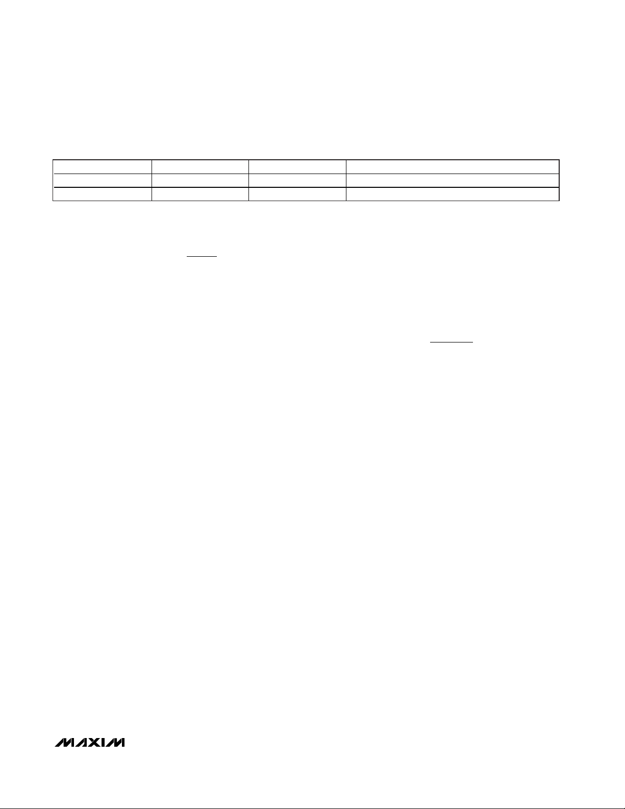
Ordering Information
19-3006; Rev 1; 2/04
For pricing, delivery, and ordering information, please contact Maxim/Dallas Direct! at
1-888-629-4642, or visit Maxim’s website at www.maxim-ic.com.
PART
TEMP RANGE
PIN-
M A XIM U M
G A I N ( d B )
MAX9750AETI†
13.5
MAX9750AEUI*
28 TSSOP 13.5
MAX9750BETI†
19.5
MAX9750BEUI*
28 TSSOP 19.5
MAX9750CETI†
10.5
MAX9750CEUI*
28 TSSOP 10.5
MAX9751ETI†
10.5
MAX9751EUI*
28 TSSOP 10.5
MAX9755AETI†
10.5
MAX9755AEUI*
28 TSSOP 10.5
*Future product—contact factory for availability.
†
Lead-free package.
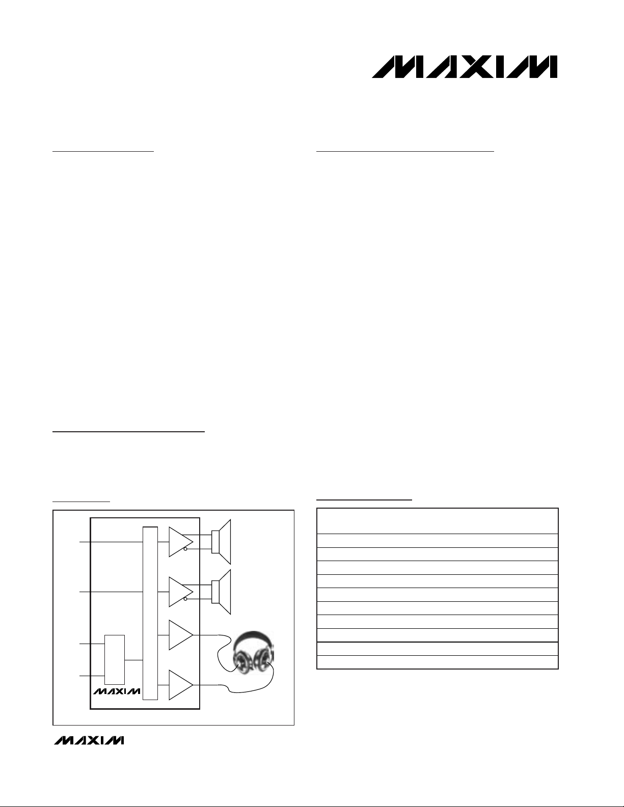
VOL
BEEP
MAX9750
Simplified Block Diagrams
Simplifed Block Diagrams continued at end of data sheet.
PACKAGE
-40°C to +85°C 28 Thi n QFN
-40°C to +85°C
-40°C to +85°C 28 Thi n QFN
-40°C to +85°C
-40°C to +85°C 28 Thi n QFN
-40°C to +85°C
-40°C to +85°C 28 Thi n QFN
-40°C to +85°C
-40°C to +85°C 28 Thi n QFN
-40°C to +85°C
Page 2
MAX9750/MAX9751/MAX9755
2.6W Stereo Audio Power Amplifiers and
DirectDrive Headphone Amplifiers
2 _______________________________________________________________________________________
ABSOLUTE MAXIMUM RATINGS
Stresses beyond those listed under “Absolute Maximum Ratings” may cause permanent damage to the device. These are stress ratings only, and functional
operation of the device at these or any other conditions beyond those indicated in the operational sections of the specifications is not implied. Exposure to
absolute maximum rating conditions for extended periods may affect device reliability.
Supply Voltage (VDD, PVDD, HPVDD, CPVDDto GND)..........+6V
GND to PGND.....................................................................±0.3V
CPV
SS
, C1N, VSSto GND .........................-6.0V to (GND + 0.3V)
HPOUT_ to GND....................................................................±3V
Any Other Pin .............................................-0.3V to (V
DD
+ 0.3V)
Duration of OUT_ Short Circuit to GND or PV
DD
........Continuous
Duration of OUT_+ Short Circuit to OUT_-.................Continuous
Duration of HPOUT_ Short Circuit to GND,
V
SS
or HPVDD.........................................................Continuous
Continuous Current (PV
DD
, OUT_, PGND) ...........................1.7A
Continuous Current (CPV
DD
, C1N, C1P, CPVSS, VSS, HPVDD,
HPOUT_).......................................................................850mA
Continuous Input Current (All Other Pins) ........................±20mA
Continuous Power Dissipation (T
A
= +70°C)
28-Pin Thin QFN (derate 20.8mW/°C above +70°C) ..1667mW
28-Pin TSSOP (derate 13mW/°C above +70°C) .........1039mW
Junction Temperature......................................................+150°C
Operating Temperature Range ...........................-40°C to +85°C
Storage Temperature Range .............................-65°C to +150°C
Lead Temperature (soldering, 10s) .................................+300°C
ELECTRICAL CHARACTERISTICS
(VDD= PVDD= CPVDD= HPVDD= 5V, GND = PGND = CPGND = 0V, SHDN = VDD, C
BIAS
= 1µF, C1 = C2 = 1µF, speaker load
terminated between OUT_+ and OUT_-, headphone load terminated between HPOUT_ and GND, GAIN1 = GAIN2 = VOL = GAIN = 0V,
T
A
= T
MIN
to T
MAX
, unless otherwise noted. Typical values are at TA= +25°C.) (Note 1)
PARAMETER
CONDITIONS
UNITS
GENERAL
Supply Voltage Range
Inferred from PSRR test 4.5 5.5 V
Headphone Supply Voltage
CPV
DD
,
HPV
DD
Inferred from PSRR test 3 5.5 V
HPS = GND, speaker mode, RL = ∞ 14 29
Quiescent Supply Current I
DD
HPS = VDD, headphone mode, RL = ∞ 713
mA
Shutdown Supply Current I
SHDN
SHDN = GND 0.2 5 µA
Bias Voltage V
BIAS
1.7 1.8 1.9 V
Switching Time t
SW
Gain or input switching 10 µs
Input Resistance R
IN
Amplifier inputs (Note 2) 10 20 30 kΩ
Turn-On Time t
SON
25 ms
SPEAKER AMPLIFIER (HPS = GND)
MAX9750A/MAX9750B/
MAX9751/MAX9755
±1 ±15
Output Offset Voltage V
OS
Measured
between OUT_+
and OUT_-
MAX9750C
±6
mV
PVDD or VDD = 4.5V to 5.5V (TA = +25°C) 75 90
f = 1kHz, V
RIPPLE
= 200mV
P-P
80
Power-Supply Rejection Ratio
(Note 3)
PSRR
f = 10kHz, V
RIPPLE
= 200mV
P-P
55
dB
SYMBOL
VDD, PV
DD
MIN TYP MAX
±0.4
Page 3
MAX9750/MAX9751/MAX9755
2.6W Stereo Audio Power Amplifiers and
DirectDrive Headphone Amplifiers
_______________________________________________________________________________________ 3
ELECTRICAL CHARACTERISTICS (continued)
(VDD= PVDD= CPVDD= HPVDD= 5V, GND = PGND = CPGND = 0V, SHDN = VDD, C
BIAS
= 1µF, C1 = C2 = 1µF, speaker load
terminated between OUT_+ and OUT_-, headphone load terminated between HPOUT_ and GND, GAIN1 = GAIN2 = VOL = GAIN = 0V,
T
A
= T
MIN
to T
MAX
, unless otherwise noted. Typical values are at TA= +25°C.) (Note 1)
PARAMETER
CONDITIONS
UNITS
MAX9750A/
MAX9750B/
MAX9751/
MAX9755
0.9 1.4
RL = 8Ω
0.8
MAX9750A/
MAX9750B/
MAX9751/
MAX9755
2.3
RL = 4Ω
1.2 1.5
MAX9750A/
MAX9750B/
MAX9751/
MAX9755
2.6
Output Power (Note 4) P
OUT
f = 1kHz,
T
A
= +25°C
R
L
= 3Ω
2.2
W
RL = 8Ω, P
OUT
= 500mW, f = 1kHz
Total Harmonic Distortion Plus
Noise
THD+N
R
L
= 4Ω, P
OUT
= 1W, f = 1kHz
%
Signal-to-Noise Ratio SNR
R
L
= 8Ω, P
OUT
= 500mW, BW = 22Hz to
22kHz
90 dB
Noise V
n
BW = 22Hz to 22kHz, A-weighted 80
µV
RMS
Capacitive-Load Drive C
L
No sustained oscillations
pF
Crosstalk L to R, R to L, f = 10kHz 75
Off-Isolation
Any unselected input to any active input,
f = 10kHz (MAX9751), input referred
75
dB
Slew Rate SR 1.4 V/µs
GAIN1 = 0, GAIN2 = 0 9
GAIN1 = 1, GAIN2 = 0
GAIN1 = 0, GAIN2 = 1 12
MAX9750A
GAIN1 = 1, GAIN2 = 1
GAIN1 = 0, GAIN2 = 0 15
GAIN1 = 1, GAIN2 = 0
GAIN1 = 0, GAIN2 = 1 18
MAX9750B
GAIN1 = 1, GAIN2 = 1
GAIN1 = 0, GAIN2 = 0 6
GAIN1 = 1, GAIN2 = 0 7.5
GAIN1 = 0, GAIN2 = 1 9
Gain (Maximum Volume Setting)
)
MAX9750C
GAIN1 = 1, GAIN2 = 1
dB
GAIN = 1 9
Gain (MAX9751/MAX9755) A
V
GAIN = 0
10.5
dB
SYMBOL
MAX9750C 0.65
THD+N = 1%,
A
VMAX(SPKR
MAX9750C
MAX9750C
MIN TYP MAX
0.01
0.02
200
10.5
13.5
16.5
19.5
10.5
Page 4
MAX9750/MAX9751/MAX9755
2.6W Stereo Audio Power Amplifiers and
DirectDrive Headphone Amplifiers
4 _______________________________________________________________________________________
ELECTRICAL CHARACTERISTICS (continued)
(VDD= PVDD= CPVDD= HPVDD= 5V, GND = PGND = CPGND = 0V, SHDN = VDD, C
BIAS
= 1µF, C1 = C2 = 1µF, speaker load
terminated between OUT_+ and OUT_-, headphone load terminated between HPOUT_ and GND, GAIN1 = GAIN2 = VOL = GAIN = 0V,
T
A
= T
MIN
to T
MAX
, unless otherwise noted. Typical values are at TA= +25°C.) (Note 1)
PARAMETER
SYMBOL
CONDITIONS
MIN
TYP
MAX
UNITS
HEADPHONE AMPLIFIER (HPS = VDD)
Output Offset Voltage V
OS
TA = +25°C ±2 ±7mV
HPVDD = 3V to 5.5V, TA = +25°C 60 75
f = 1kHz, V
RIPPLE
= 200mV
P-P
73
Power-Supply Rejection Ratio
(Note 3)
PSRR
f = 10kHz, V
RIPPLE
= 200mV
P-P
63
dB
RL = 32Ω 40 50
Output Power P
OUT
THD+N = 1%,
f = 1kHz, T
A
= +25°C
R
L
= 16Ω
mW
RL = 32Ω, P
OUT
= 20mW, f = 1kHz
Total Harmonic Distortion Plus
Noise
THD+N
R
L
= 16Ω, P
OUT
= 75mW, f = 1kHz
%
Signal-to-Noise Ratio SNR
R
L
= 32Ω, P
OUT
= 50mW, BW = 22Hz to
22kHz
95 dB
Noise V
n
BW = 22Hz to 22kHz 12
µV
RMS
Capacitive-Load Drive C
L
No sustained oscillations
pF
Crosstalk L to R, R to L, f = 10kHz 88
Off-Isolation
Any unselected input to any active input,
f = 10kHz (MAX9751), input referred
74
dB
Slew Rate SR 0.4 V/µs
ESD ESD IEC air discharge ±8 kV
GAIN2 = GAIN = 0, GAIN1 = X 0
Gain A
V
GAIN2 = GAIN = 1, GAIN1 = X 3
dB
CHARGE PUMP
Charge-Pump Frequency f
OSC
600 kHz
VOLUME CONTROL (MAX9750_)
VOL Input Impedance R
VOL
MΩ
VOL Input Hysteresis 10 mV
Full Mute Input Voltage (Note 5)
0.858 x
V
Channel Matching AV = -25dB to +13.5dB
dB
BEEP INPUT (MAX9750_)
Beep Signal Minimum Amplitude
V
BEEP
RB = 33kΩ (Note 6) 0.8 V
P-P
Beep Signal Minimum Frequency
f
BEEP
Hz
110
0.007
0.03
200
500 550
100
HPV
400
±0.2
DD
Page 5
MAX9750/MAX9751/MAX9755
2.6W Stereo Audio Power Amplifiers and
DirectDrive Headphone Amplifiers
_______________________________________________________________________________________ 5
ELECTRICAL CHARACTERISTICS (continued)
(VDD= PVDD= CPVDD= HPVDD= 5V, GND = PGND = CPGND = 0V, SHDN = VDD, C
BIAS
= 1µF, C1 = C2 = 1µF, speaker load
terminated between OUT_+ and OUT_-, headphone load terminated between HPOUT_ and GND, GAIN1 = GAIN2 = VOL = GAIN = 0V,
T
A
= T
MIN
to T
MAX
, unless otherwise noted. Typical values are at TA= +25°C.) (Note 1)
PARAMETER
CONDITIONS
UNITS
LOGIC INPUT (SHDN, GAIN1, GAIN2, GAIN, VOL, IN1/2)
Logic Input High Voltage V
IH
2V
Logic Input Low Voltage V
IL
0.8 V
Logic Input Current I
IN
±1µA
LOGIC INPUT HEADPHONE (HPS)
Logic Input High Voltage V
IH
2V
Logic Input Low Voltage V
IL
0.8 V
Logic Input Current I
IN
10 µA
Note 1: All devices are 100% production tested at room temperature. All temperature limits are guaranteed by design.
Note 2: Guaranteed by design. Not production tested.
Note 3: PSRR is specified with the amplifier input connected to GND through C
IN
.
Note 4: Output power levels are measured with the thin QFN’s exposed paddle soldered to the ground plane.
Note 5: See Table 3 for details of the mute levels.
Note 6: The value of R
B
dictates the minimum beep signal amplitude (see the Beep Input section).
SYMBOL
MIN TYP MAX
Page 6
MAX9750/MAX9751/MAX9755
2.6W Stereo Audio Power Amplifiers and
DirectDrive Headphone Amplifiers
6 _______________________________________________________________________________________
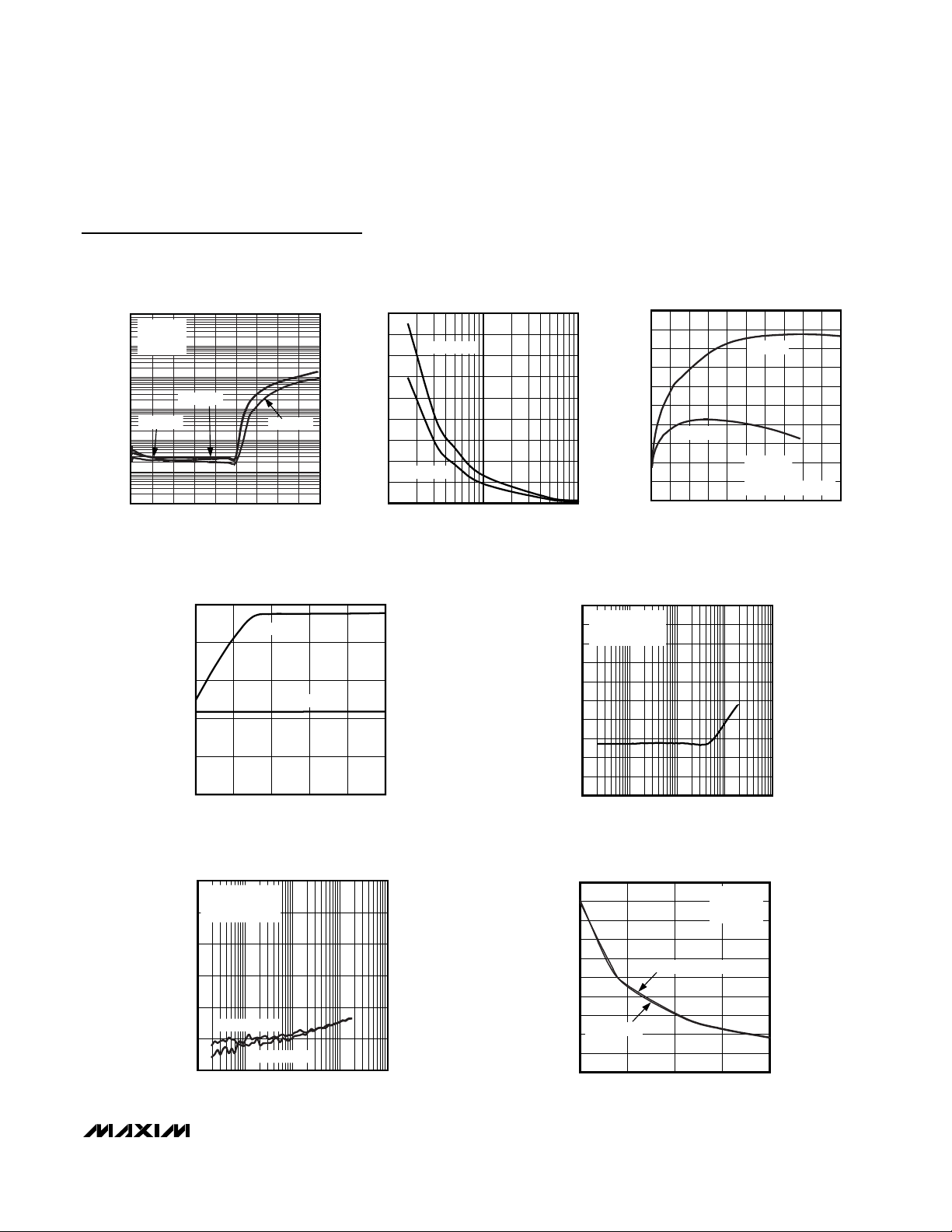
Typical Operating Characteristics
(Measurement BW = 22Hz to 22kHz, TA = +25°C, unless otherwise noted.)
10
1
0.1
0.01
0.001
0.0001
10 1k 10k100 100k
TOTAL HARMONIC DISTORTION PLUS NOISE
vs. FREQUENCY (SPEAKER MODE)
MAX9750/51 toc01
FREQUENCY (Hz)
THD+N (%)
VCC = 5V
R
L
= 3Ω
A
V
= 10.5dB
OUTPUT POWER = 1.5W
OUTPUT POWER = 500mW
10
1
0.1
0.01
0.001
0.0001
10 1k 10k100 100k
TOTAL HARMONIC DISTORTION PLUS NOISE
vs. FREQUENCY (SPEAKER MODE)
MAX9750/51 toc02
FREQUENCY (Hz)
THD+N (%)
VCC = 5V
R
L
= 4Ω
A
V
= 10.5dB
OUTPUT POWER = 1.25W
OUTPUT POWER = 500mW
10
1
0.1
0.01
0.001
0.0001
10 1k 10k100 100k
TOTAL HARMONIC DISTORTION PLUS NOISE
vs. FREQUENCY (SPEAKER MODE)
MAX9750/51 toc03
FREQUENCY (Hz)
THD+N (%)
VCC = 5V
R
L
= 8Ω
A
V
= 10.5dB
OUTPUT POWER = 100mW
OUTPUT POWER = 600mW
100
00.51.01.5 2.0 2.5 3.0
10
1
0.1
0.01
0.001
TOTAL HARMONIC DISTORTION PLUS NOISE
vs. OUTPUT POWER (SPEAKER MODE)
MAX9750/51 toc04
OUTPUT POWER (W)
THD+N (%)
VCC = 5V
R
L
= 3Ω
A
V
= 10.5dB
MAX9750C
fIN = 10kHz
fIN = 1kHz
fIN = 20Hz
TOTAL HARMONIC DISTORTION PLUS NOISE
vs. OUTPUT POWER (SPEAKER MODE)
MAX9750/51 toc05
OUTPUT POWER (W)
THD+N (%)
3.53.02.52.01.51.00.5
0.01
0.1
1
10
100
0.001
0
VDD = 5V
A
V
= 13.5dB
R
L
= 3Ω
f = 1kHz
f = 10kHz
f = 20Hz
100
0
0.5
1.0 1.5
2.0
10
1
0.1
0.01
0.001
TOTAL HARMONIC DISTORTION PLUS NOISE
vs. OUTPUT POWER (SPEAKER MODE)
MAX9750/51 toc06
OUTPUT POWER (W)
THD+N (%)
fIN = 1kHz
fIN = 20Hz
VCC = 5V
R
L
= 4Ω
A
V
= 10.5dB
MAX9750C
fIN = 10kHz
TOTAL HARMONIC DISTORTION PLUS NOISE
vs. OUTPUT POWER (SPEAKER MODE)
MAX9750/51 toc07
OUTPUT POWER (W)
THD+N (%)
2.52.01.51.00.5
0.01
0.1
1
10
100
0.001
0 3.0
VDD = 5V
A
V
= 13.5dB
R
L
= 4Ω
f = 1kHz
f = 10kHz
f = 20Hz
100
0
0.2 0.4 0.6
0.8 1.0
1.2
10
1
0.1
0.01
0.001
TOTAL HARMONIC DISTORTION PLUS NOISE
vs. OUTPUT POWER (SPEAKER MODE)
MAX9750/51 toc08
OUTPUT POWER (W)
THD+N (%)
fIN = 20Hz
fIN = 1kHz
fIN = 10kHz
VCC = 5V
R
L
= 8Ω
A
V
= 10.5dB
MAX9750C
TOTAL HARMONIC DISTORTION PLUS NOISE
vs. OUTPUT POWER (SPEAKER MODE)
MAX9750/51 toc09
OUTPUT POWER (W)
THD+N (%)
1.51.00.5
0.01
0.1
1
10
100
0.001
0
VDD = 5V
A
V
= 13.5dB
R
L
= 8Ω
f = 1kHz
f = 10kHz
f = 20Hz
Page 7
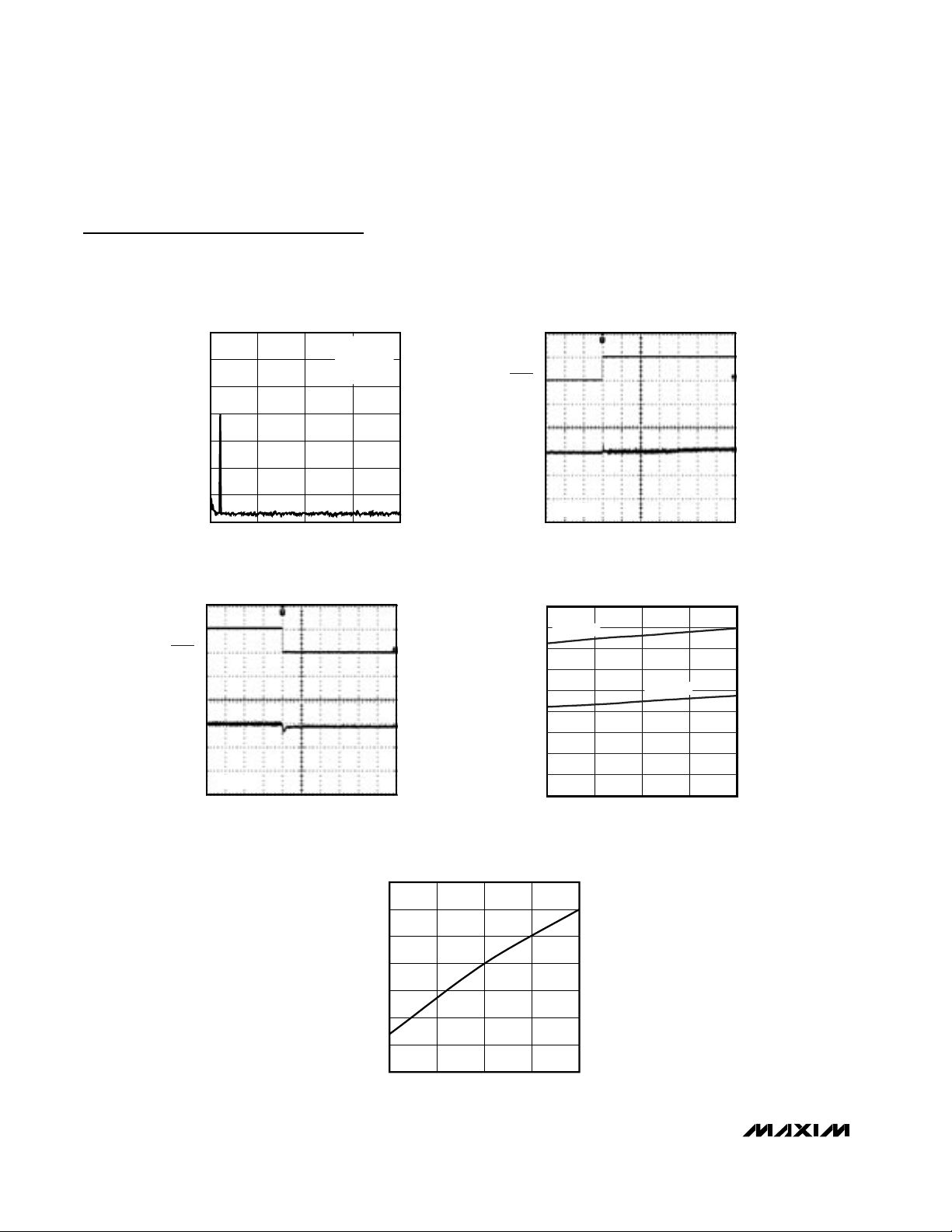
Typical Operating Characteristics (continued)
(Measurement BW = 22Hz to 22kHz, TA = +25°C, unless otherwise noted.)
MAX9750/MAX9751/MAX9755
2.6W Stereo Audio Power Amplifiers and
DirectDrive Headphone Amplifiers
_______________________________________________________________________________________ 7
OUTPUT POWER
vs. LOAD RESISTANCE (SPEAKER MODE)
MAX9750/51 toc10
LOAD RESISTANCE (Ω)
OUTPUT POWER (W)
10
0.5
1.0
1.5
2.0
2.5
3.0
3.5
0
1 100
THD+N = 10%
THD+N = 1%
OUTPUT POWER
vs. LOAD RESISTANCE (SPEAKER MODE)
MAX9750/51 toc11
LOAD RESISTANCE (Ω)
OUTPUT POWER (W)
3.0
0
0.5
1.0
1.5
2.0
2.5
110100
THD+N = 10%
THD+N = 1%
VCC = 5V
f = 1kHz
A
V
= 10.5dB
MAX9750C
POWER DISSIPATION vs. OUTPUT POWER
(SPEAKER MODE)
MAX9750/51 toc12
OUTPUT POWER (W)
POWER DISSIPATION (W)
321
1
2
3
4
5
0
04
RL = 4Ω
RL = 8Ω
VDD = 5V
f = 1kHz
P
OUT
= P
OUTL
+ P
OUTR
POWER DISSIPATION vs. OUTPUT POWER
(SPEAKER MODE)
MAX9750/51 toc13
OUTPUT POWER (W)
POWER DISSIPATION (mW)
3.53.02.52.01.51.00.5
1
2
3
4
5
0
04.0
RL = 4Ω
RL = 8Ω
VDD = 5V
f = 1kHz
P
OUT
= P
OUTL
+ P
OUTR
MAX9750C
POWER-SUPPLY REJECTION RATIO
vs. FREQUENCY (SPEAKER MODE)
MAX9750/51 toc14
FREQUENCY (Hz)
PSRR (dB)
10k1k100
-90
-80
-70
-60
-50
-40
-30
-20
-10
0
-100
10 100k
V
RIPPLE
= 200mV
P-P
AV = 10.5dB
OUTPUT REFERRED
0
-120
10 1k 10k100 100k
CROSSTALK vs. FREQUENCY
(SPEAKER MODE)
MAX9750/51 toc15
FREQUENCY (Hz)
CROSSTALK (dB)
-100
-110
-80
-90
-60
-70
-40
-50
-20
-10
-30
VCC = 5V
V
RIPPLE
= 200mV
P-P
RL = 4Ω
LEFT TO RIGHT
RIGHT TO LEFT
TURN-ON RESPONSE
(SPEAKER MODE)
MAX9750/51 toc16
20ms/div
SHDN
5V/div
2V/div
100mV/div
OUT_+
AND
OUT_-
OUT_+
- OUT_-
RL = 8Ω
Page 8
Typical Operating Characteristics (continued)
(Measurement BW = 22Hz to 22kHz, TA = +25°C, unless otherwise noted.)
MAX9750/MAX9751/MAX9755
2.6W Stereo Audio Power Amplifiers and
DirectDrive Headphone Amplifiers
8 _______________________________________________________________________________________
10
1
0.1
0.01
0.001
0.0001
10 1k 10k100 100k
TOTAL HARMONIC DISTORTION PLUS NOISE
vs. FREQUENCY (HEADPHONE MODE)
MAX9750/51 toc19
THD+N (%)
VDD = 5V
R
L
= 32Ω
A
V
= 3dB
OUTPUT POWER = 45mW
OUTPUT POWER = 10mW
10
1
0.1
0.01
0.001
0.0001
10 1k 10k100 100k
TOTAL HARMONIC DISTORTION PLUS NOISE
vs. FREQUENCY (HEADPHONE MODE)
MAX9750/51 toc20
THD+N (%)
VDD = 3.3V
R
L
= 16Ω
A
V
= 3dB
OUTPUT POWER = 30mW
OUTPUT POWER = 10mW
10
1
0.1
0.01
0.001
0.0001
10 1k 10k100 100k
TOTAL HARMONIC DISTORTION PLUS NOISE
vs. FREQUENCY (HEADPHONE MODE)
MAX9750/51 toc21
THD+N (%)
VDD = 3.3V
R
L
= 32Ω
A
V
= 3dB
OUTPUT POWER = 45mW
OUTPUT POWER = 10mW
1000
100
10
1
0.1
0.01
0.001
075
100
12550
25
15
TOTAL HARMONIC DISTORTION PLUS NOIS
vs. OUTPUT POWER (HEADPHONE MODE
OUTPUT POWER (mW)
THD+N (%)
VDD = 5V
R
L
= 16Ω
A
V
= 3dB
f
IN
= 10kHz
f
IN
= 1kHz
f
IN
= 20Hz
1000
100
10
1
0.1
0.01
0.001
0608040
20
100
TOTAL HARMONIC DISTORTION PLUS NOISE
vs. OUTPUT POWER (HEADPHONE MODE)
MAX9750/51 toc23
OUTPUT POWER (mW)
THD+N (%)
VDD = 5V
R
L
= 32Ω
A
V
= 3dB
f
IN
= 10kHz
f
IN
= 1kHz
f
IN
= 20Hz
1000
100
10
1
0.1
0.01
0.001
030
40
5020
10
60
TOTAL HARMONIC DISTORTION PLUS NOISE
vs. OUTPUT POWER (HEADPHONE MODE)
MAX9750/51 toc24
OUTPUT POWER (mW)
THD+N (%)
VDD = 3.3V
R
L
= 16Ω
A
V
= 3dB
f
IN
= 10kHz
f
IN
= 1kHz
f
IN
= 20Hz
TURN-OFF RESPONSE
(SPEAKER MODE)
MAX9750/51 toc17
20ms/div
SHDN
5V/div
2V/div
20mV/div
OUT_+
AND
OUT_-
OUT_+
- OUT_-
RL = 8Ω
10
1
0.1
0.01
0.001
0.0001
10 1k 10k100 100k
TOTAL HARMONIC DISTORTION PLUS NOISE
vs. FREQUENCY (HEADPHONE MODE)
MAX9750/51 toc18
FREQUENCY (Hz)
THD+N (%)
VDD = 5V
R
L
= 16Ω
A
V
= 3dB
OUTPUT POWER = 90mW
OUTPUT POWER = 30mW
Page 9
MAX9750/MAX9751/MAX9755
2.6W Stereo Audio Power Amplifiers and
DirectDrive Headphone Amplifiers
_______________________________________________________________________________________ 9
OUTPUT POWER vs. SUPPLY VOLTAGE
(HEADPHONE MODE)
MAX9750/51 toc28
SUPPLY VOLTAGE (V)
OUTPUT POWER (mW)
5.04.54.03.5
25
50
75
100
125
0
3.0 5.5
RL = 16Ω
RL = 32Ω
f = 1kHz
10 1k 10k100 100k
POWER-SUPPLY REJECTION RATIO
vs. FREQUENCY (HEADPHONE MODE)
MAX9750/51 toc29
FREQUENCY (Hz)
PSRR (dB)
V
RIPPLE
= 200mV
P-P
AV = 10.5dB
OUTPUT REFERRED
-90
-80
-70
-60
-50
-40
-30
-20
-10
0
-100
10 100 1k 10k 100k
CROSSTALK vs. FREQUENCY
(HEADPHONE MODE)
MAX9750/51 toc30
FREQUENCY (Hz)
CROSSTALK (dB)
VCC = 5V
V
RIPPLE
= 200mV
P-P
RL = 32Ω
LEFT TO RIGHT
RIGHT TO LEFT
-100
-80
-60
-40
-20
0
-120
OUTPUT POWER vs. CHARGE-PUMP
CAPACITANCE AND LOAD RESISTANCE
MAX9750/51 toc31
LOAD RESISTANCE (Ω)
OUTPUT POWER (mW)
403020
20
40
60
80
100
120
140
160
180
200
0
10 50
VDD = 5V
f = 1kHz
THD+N = 1%
C1 = C2 = 2.2µF
C1 = C2 = 1µF
Typical Operating Characteristics (continued)
(Measurement BW = 22Hz to 22kHz, TA = +25°C, unless otherwise noted.)
OUTPUT POWER vs. LOAD RESISTANCE
(HEADPHONE MODE)
MAX9750/51 toc26
LOAD RESISTANCE (Ω)
OUTPUT POWER (mW)
100
20
40
60
80
100
120
140
160
180
0
10 1000
THD+N = 10%
THD+N = 1%
(HEADPHONE MODE)
MAX9750/51 toc27
OUTPUT POWER (mW)
POWER DISSIPATION (mW)
225200150 17550 75 100 12525
25
50
75
100
125
150
175
200
225
250
0
0250
VDD = 5V
f = 1kHz
P
OUT
= P
OUTL
+ P
OUTR
R
L
= 16Ω
R
L
= 32Ω
1000
100
10
0.1
1
0.01
0.001
070
80
20 30
40
50
60
10
90
TOTAL HARMONIC DISTORTION PLUS NOISE
vs. OUTPUT POWER (HEADPHONE MODE)
MAX9750/51 toc25
OUTPUT POWER (mW)
THD+N (%)
VDD = 3.3V
R
L
= 32Ω
A
V
= 3dB
f
IN
= 10kHz
f
IN
= 1kHz
f
IN
= 20Hz
Page 10
MAX9750/MAX9751/MAX9755
2.6W Stereo Audio Power Amplifiers and
DirectDrive Headphone Amplifiers
10 ______________________________________________________________________________________
HEADPHONE OUTPUT SPECTRUM
MAX9750/51 toc32
FREQUENCY (Hz)
MAGNITUDE (dB)
15105
0
020
-120
-100
-80
-60
-40
-20
-140
VDD = 5V
f = 1kHz
V
OUT
= -60dB
R
L
= 32Ω
TURN-ON RESPONSE
(HEADPHONE MODE)
MAX9750/51 toc33
10ms/div
SHDN
5V/div
20mV/div
HPOUT_
RL = 32Ω
TURN-OFF RESPONSE
(HEADPHONE MODE)
MAX9750/51 toc34
10ms/div
SHDN
5V/div
20mV/div
HPOUT_
RL = 32Ω
SUPPLY CURRENT
vs. SUPPLY VOLTAGE
MAX9750/51 toc35
SUPPLY VOLTAGE (V)
SUPPLY CURRENT (mA)
5.255.004.75
4
2
6
8
12
10
14
16
18
0
4.50 5.50
HPS = GND
HPS = V
DD
SHUTDOWN SUPPLY CURRENT
vs. SUPPLY VOLTAGE
MAX9750/51 toc36
SUPPLY VOLTAGE (V)
SUPPLY CURRENT (
µ
A)
5.255.004.754.50 5.50
0.05
0.10
0.15
0.20
0.25
0.30
0.35
0
Typical Operating Characteristics (continued)
(Measurement BW = 22Hz to 22kHz, TA = +25°C, unless otherwise noted.)
Page 11
MAX9750/MAX9751/MAX9755
2.6W Stereo Audio Power Amplifiers and
DirectDrive Headphone Amplifiers
______________________________________________________________________________________ 11
Pin Description
PIN
MAX9750 MAX9751 MAX9755
THIN
QFN
THIN
THIN
NAME FUNCTION
15—— 26INL Left-Channel Audio Input
26————BEEP Audible Alert Beep Input
3, 19
PGND Power Ground
484848
Left-Channel Positive Speaker Output
595959OUTL- Left-Channel Negative Speaker Output
6, 16
PV
DD
Speaker Amplifier Power Supply
711711711
Charge-Pump Power Supply
812812 8 12 C1P Charge-Pump Flying-Capacitor Positive Terminal
913913913
Charge-Pump Ground
10 14 10 14 10 14 C1N Charge-Pump Flying-Capacitor Negative Terminal
11 15 11 15 11 15 CPV
SS
Charge-Pump Output. Connect to VSS.
12 16 12 16 12 16 V
SS
Headphone Amplifier Negative Power Supply
13 17 13 17 13 17
Right-Channel Headphone Output
14 18 14 18 14 18
Left-Channel Headphone Output
15 19 15 19 15 19
Headphone Positive Power Supply
17 21 17 21 17 21 OUTR- Right-Channel Negative Speaker Output
18 22 18 22 18 22
Right-Channel Positive Speaker Output
20 24 20 24 20 24 HPS Headphone Sense Input
21 25 21 25 21 25 BIAS
Common-Mode Bias Voltage. Bypass with a 1µF
capacitor to GND.
22 26 22 26 22 26 SHDN
Shutdown. Drive SHDN low to disable the device.
Connect SHDN to V
DD
for normal operation.
23 27 ————GAIN2Gain Control Input 2
24 28 ————GAIN1Gain Control Input 1
25 1 25 1 25 1 V
DD
Power Supply
26 2 26 2
GND Ground
27 3 — — 28 4 INR Right-Channel Audio Input
28 4 ————VOLAnalog Volume Control Input
—— 15——INL1 Left-Channel Audio Input 1
—— 26——INL2 Left-Channel Audio Input 2
——23 27 — — IN1/2 Input Select
——24 28 24 28 GAIN Gain Select
——27 3 — — INR1 Right-Channel Audio Input 1
——28 4 — — INR2 Right-Channel Audio Input 2
————
3, 5 N.C. No Connection. Not internally connected.
TSSOP
QFN
23, 26 2, 27
1, 27
TSSOP
7, 23 3, 19 7, 23 3, 19 7, 23
10, 20 6, 16 10, 20 6, 16 10, 20
QFN
TSSOP
OUTL+
CPV
DD
CPGND
HPOUTR
HPOUTL
HPV
DD
OUTR+
Page 12

MAX9750/MAX9751/MAX9755
2.6W Stereo Audio Power Amplifiers and
DirectDrive Headphone Amplifiers
12 ______________________________________________________________________________________
Detailed Description
The MAX9750/MAX9751/MAX9755 combine a 2.6W BTL
speaker amplifier and a 110mW DirectDrive headphone
amplifier with integrated headphone sensing and comprehensive click-and-pop suppression. The MAX9750
features an analog volume control, BEEP input, and
four-level gain control. The MAX9751 features a 2:1
input stereo multiplexer and two-level gain control. All
devices feature high 90dB PSRR, low 0.01% THD+N,
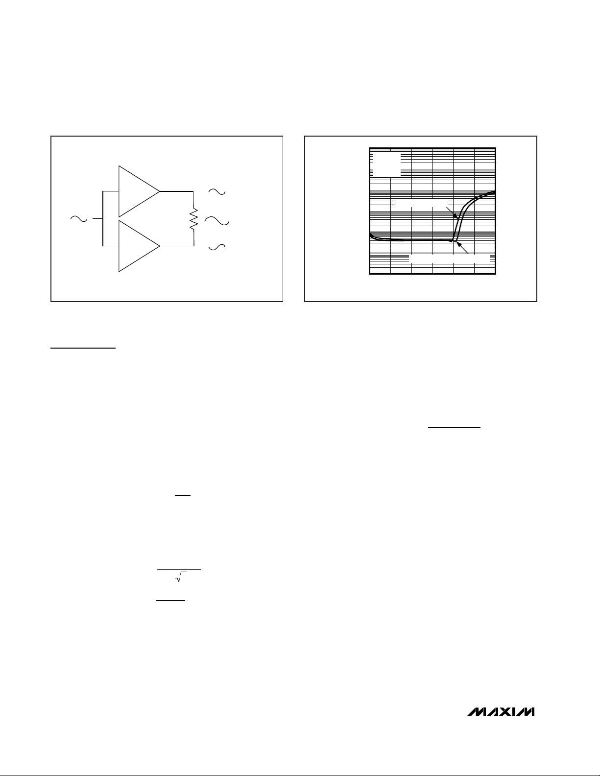
industry-leading click-pop performance, and a lowpower shutdown mode.
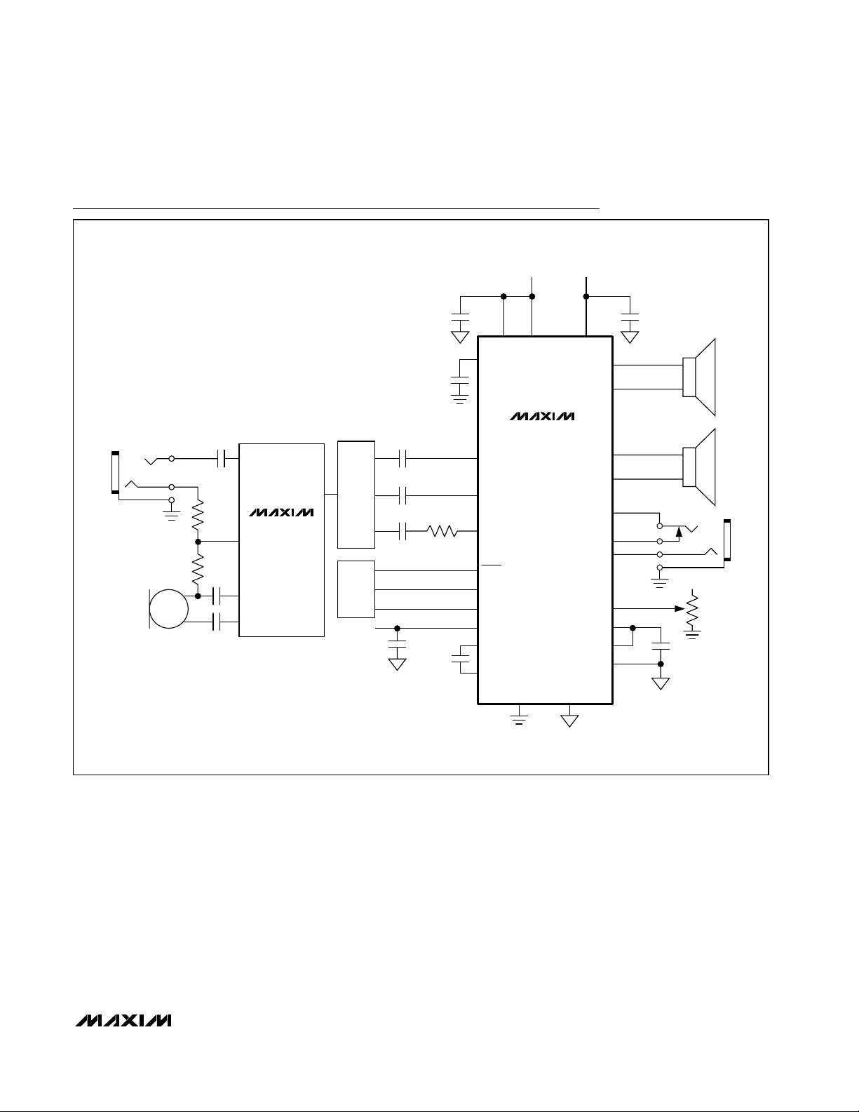
Each signal path consists of an input amplifier that sets
the gain of the signal path and feeds both the speaker
and headphone amplifier (Figure 1). The speaker
amplifier uses a BTL architecture, doubling the voltage
drive to the speakers and eliminating the need for DCblocking capacitors. The output consists of two signals,
identical in magnitude, but 180° out of phase.
The headphone amplifiers use Maxim’s patented
DirectDrive architecture that eliminates the bulky output
DC-blocking capacitors required by traditional headphone amplifiers. A charge pump inverts the positive
supply (CPVDD), creating a negative supply (CPVSS).
The headphone amplifiers operate from these bipolar
supplies with their outputs biased about GND (Figure 2).
The amplifiers have almost twice the supply range
compared to other single-supply amplifiers, nearly quadrupling the available output power. The benefit of the
GND bias is that the amplifier outputs no longer have a
DC component (typically V
DD
/ 2). This eliminates the
large DC-blocking capacitors required with conventional headphone amplifiers, conserving board space and
system cost, and improving frequency response.
The MAX9750 features an analog volume control that
varies the gain of the amplifiers based on the DC voltage applied at VOL. Both devices feature an undervoltage lockout that prevents operation from an insufficient
power supply and click-and-pop suppression that eliminates audible transients on startup and shutdown. The
amplifiers include thermal-overload and short-circuit
protection, and can withstand ±8kV ESD strikes on the
headphone amplifier outputs (IEC air discharge). An
additional feature of the speaker amplifiers is that there
is no phase inversion from input to output.
DirectDrive
Conventional single-supply headphone amplifiers have
their outputs biased about a nominal DC voltage (typically half the supply) for maximum dynamic range.
Large coupling capacitors are needed to block this DC
bias from the headphones. Without these capacitors, a
OUT_+
OUT_
VOLUME
CONTROL
BIAS
IN_
VOL
BIAS
MAX9750 ONLY
BIAS
HPOUT_
GND
Figure 1. MAX9750/MAX9751 Signal Path
+V
DD
-V
DD
GND
CONVENTIONAL DRIVER-BIASING SCHEME
DirectDrive BIASING SCHEME
VDD/2
V
DD
GND
V
OUT
Figure 2. Traditional Headphone Amplifier Output Waveform
vs. DirectDrive Headphone Amplifier Output Waveform
Page 13

MAX9750/MAX9751/MAX9755
2.6W Stereo Audio Power Amplifiers and
DirectDrive Headphone Amplifiers
______________________________________________________________________________________ 13
significant amount of DC current flows to the headphone,
resulting in unnecessary power dissipation and possible
damage to both headphone and headphone amplifier.
Maxim’s patented DirectDrive architecture uses a charge
pump to create an internal negative supply voltage. This
allows the MAX9750/MAX9751/MAX9755 headphone
amplifier output to be biased about GND, almost doubling the dynamic range while operating from a single
supply. With no DC component, there is no need for the
large DC-blocking capacitors. Instead of two large
capacitors (220µF typ), the MAX9750/MAX9751/
MAX9755 charge pump requires only two small ceramic
capacitors (1µF typ), conserving board space, reducing
cost, and improving the frequency response of the headphone amplifier. See the Output Power vs. Charge-Pump
Capacitance and Load Resistance graph in the Typical
Operating Characteristics for details of the possible
capacitor values.
Previous attempts to eliminate the output coupling
capacitors involved biasing the headphone return
(sleeve) to the DC bias voltage of the headphone
amplifiers. This method raised some issues:
1) The sleeve is typically grounded to the chassis. Using
this biasing approach, the sleeve must be isolated
from system ground, complicating product design.
2) During an ESD strike, the amplifier’s ESD structures
are the only path to system ground. The amplifier
must be able to withstand the full ESD strike.
3) When using the headphone jack as a lineout to other
equipment, the bias voltage on the sleeve may conflict with the ground potential from other equipment,
resulting in large ground-loop current and possible
damage to the amplifiers.
Low-Frequency Response
In addition to the cost and size disadvantages, the DCblocking capacitors limit the low-frequency response of
the amplifier and distort the audio signal:
1) The impedance of the headphone load to the DCblocking capacitor forms a highpass filter with the
-3dB point determined by:
where R
L
is the impedance of the headphone and
C
OUT
is the value of the DC-blocking capacitor.
The highpass filter is required by conventional single-ended, single-supply headphone amplifiers to
block the midrail DC component of the audio signal
from the headphones. Depending on the -3dB point,
the filter can attenuate low-frequency signals within
the audio band. Larger values of C
OUT
reduce the
attenuation but are physically larger, more expensive capacitors. Figure 3 shows the relationship
between the size of C
OUT
and the resulting low-frequency attenuation. Note that the -3dB point for a
16Ω headphone with a 100µF blocking capacitor is
100Hz, well within the audio band.
2) The voltage coefficient of the capacitor, the change
in capacitance due to a change in the voltage
across the capacitor, distorts the audio signal. At
frequencies around the -3dB point, the reactance of
the capacitor dominates, and the voltage coefficient
appears as frequency-dependent distortion. Figure
4 shows the THD+N introduced by two different
capacitor dielectrics. Note that around the -3dB
point, THD+N increases dramatically.
The combination of low-frequency attenuation and frequency-dependent distortion compromises audio
reproduction. DirectDrive improves low-frequency
reproduction in portable audio equipment that emphasizes low-frequency effects such as multimedia laptops, and MP3, CD, and DVD players.
Charge Pump
The MAX9750/MAX9751/MAX9755 feature a low-noise
charge pump. The 550kHz switching frequency is well
beyond the audio range, and does not interfere with the
audio signals. The switch drivers feature a controlled
switching speed that minimizes noise generated by turnon and turn-off transients. Limiting the switching speed of
the charge pump minimizes the di/dt noise caused by the
f
RC
dB
LOUT
−=3
1
2π
0
-30
10 100 1k 10k 100k
LOW-FREQUENCY ROLLOFF
(R
L
= 16Ω)
-24
-27
-12
-15
-18
-21
-6
-9
-3
FREQUENCY (Hz)
ATTENUATION (dB)
DirectDrive
330µF
220µF
100µF
33µF
Figure 3. Low-Frequency Attenuation of Common DC-Blocking
Capacitor Values
Page 14

MAX9750/MAX9751/MAX9755
2.6W Stereo Audio Power Amplifiers and
DirectDrive Headphone Amplifiers
14 ______________________________________________________________________________________
parasitic bond wire and trace inductance. Although not
typically required, additional high-frequency ripple attenuation can be achieved by increasing the size of C2 (see
the Typical Application Circuit).
Headphone Sense Input (HPS)
The headphone sense input (HPS) monitors the headphone jack and automatically configures the device
based upon the voltage applied at HPS. A voltage of
less than 0.8V sets the device to speaker mode. A voltage of greater than 2V disables the bridge amplifiers
and enables the headphone amplifiers.
For automatic headphone detection, connect HPS to the
control pin of a 3-wire headphone jack as shown in
Figure 5. With no headphone present, the output impedance of the headphone amplifier pulls HPS low. When a
headphone plug is inserted into the jack, the control pin
is disconnected from the tip contact and HPS is pulled
to VDDthrough a 10µA current source.
BIAS
The MAX9750/MAX9751/MAX9755 feature an internally
generated, power-supply independent, common-mode
bias voltage of 1.8V referenced to GND. BIAS provides
both click-and-pop suppression and sets the DC bias
level for the amplifiers. Choose the value of the bypass
capacitor as described in the BIAS Capacitor section.
No external load should be applied to BIAS. Any load
lowers the BIAS voltage, affecting the overall performance of the device.
Gain Selection
MAX9750
The MAX9750 features an internally set, selectable gain.
The GAIN1 and GAIN2 inputs set the maximum gain of
the MAX9750 speaker and headphone amplifiers (Table
1). The gain of the device can vary based upon the voltage at VOL (see the Analog Volume Control section).
However, the maximum gain cannot be exceeded.
MAX9751/MAX9755
The gain of the MAX9751/MAX9755 is set by the GAIN
input. Driving GAIN high sets the gain of the speaker
amplifiers to 9dB and the gain of the headphone amplifiers to 0dB. Driving GAIN low sets the gain of the
speaker amplifiers to 10.5dB, and the gain of the headphone amplifiers to 3dB (Table 2).
Analog Volume Control (VOL)
The MAX9750 features an analog volume control that
varies the gain of the device in 31 discrete steps based
upon the DC voltage applied to VOL. The input range of
V
VOL
is from 0 (full volume) to 0.858 x HPVDD(full mute),
with example step sizes shown in Table 3. Connect the
reference of the device driving VOL (Figure 6) to HPVDD.
Since the volume control ADC is ratiometric to HPVDD,
any changes in HPVDDare negated. The gain step sizes
are not constant; the step sizes are 0.5dB/step at the
upper extreme, 2dB/step in the midrange, and 4dB/step
at the lower extreme. Figure 7 shows the transfer function
of the volume control for a 3.3V supply.
ADDITIONAL THD+N DUE
TO DC-BLOCKING CAPACITORS
FREQUENCY (Hz)
THD+N (%)
10k1k100
0.001
0.01
0.1
1
10
0.0001
10 100k
TANTALUM
ALUM/ELEC
Figure 4. Distortion Contributed by DC-Blocking Capacitors
MAX9750/
MAX9751/
MAX9755
10µA
1kΩ1kΩ
20
14
13
V
DD
HPS
HPOUTL
HPOUTR
SHUTDOWN
CONTROL
Figure 5. HPS Configuration
Page 15
MAX9750/MAX9751/MAX9755
2.6W Stereo Audio Power Amplifiers and
DirectDrive Headphone Amplifiers
______________________________________________________________________________________ 15
BEEP Input
The MAX9750 features an audible alert beep input
(BEEP) that accepts a mono system alert signal and
mixes it into the stereo audio path. When the amplitude
of V
BEEP(OUT)
exceeds 800mV
P-P
(Figure 8) and the
frequency of the beep signal is greater than 400Hz, the
beep signal is mixed into the active audio path (speaker
or headphone). If the signal at V
BEEP(OUT)
is either
<800mV
P-P
or <400Hz, the BEEP signal is not mixed into
the audio path. The amplitude of the BEEP signal at the
device output is roughly the amplitude of V
BEEP(OUT)
times the gain of the selected signal path.
The input resistor (RB) sets the gain of the BEEP input
amplifier, and thus the amplitude of V
BEEP(OUT)
. Choose
R
B
based on:
where R
INT
is the value of the BEEP amplifier feedback
resistor (47kΩ) and VINis the BEEP input amplitude.
Note that the BEEP amplifier can be set up as either an
attenuator, if the original alert signal amplitude is too
large, or set to gain up the alert signal if it is below
800mV
P-P
. AC couple the alert signal to BEEP. Choose
the value of the coupling capacitor as described in the
Input Filtering section. Multiple beep inputs can be
summed (Figure 8).
Input Multiplexer
The MAX9751 features a 2:1 input multiplexer on each
amplifier, allowing input selection between two stereo
sources. The logic input IN1/2 controls both multiplex-
ers. A logic high selects input IN_1 and a logic low
selects input IN_2.
Shutdown
The MAX9750/MAX9751/MAX9755 features a 0.2µA,
low-power shutdown mode that reduces quiescent current consumption and extends battery life. Driving
SHDN low disables the drive amplifiers, bias circuitry,
and charge pump, and drives BIAS and all outputs to
GND. Connect SHDN to V
DD
for normal operation.
Click-and-Pop Suppression
Speaker Amplifier
The MAX9750/MAX9751/MAX9755 speaker amplifiers
feature Maxim’s comprehensive, industry-leading clickand-pop suppression. During startup, the click-pop
suppression circuitry eliminates any audible transient
sources internal to the device. When entering shutdown, both amplifier outputs ramp to GND quickly and
simultaneously.
R
VR
B
IN INT
.
≤
×
08
MAX9750
V
REF
DAC
HPV
DD
VOL
Figure 6. Volume Control Circuit
GAIN
SPEAKER MODE
GAIN (dB)
HEADPHONE
MODE GAIN (dB)
0 10.5 0
19 3
Table 2. MAX9751 Gain Settings
SPEAKER MODE GAIN (dB)
GAIN1
GAIN2
MAX9750A MAX9750B MAX9750C
HEADPHONE MODE GAIN (dB)
00 9 15 6 0
01 12 18 9 3
10 10.5 16.5 7.5 0
11 13.5 19.5 10.5 3
Table 1. MAX9750 Maximum Gain Settings
Page 16
MAX9750/MAX9751/MAX9755
2.6W Stereo Audio Power Amplifiers and
DirectDrive Headphone Amplifiers
16 ______________________________________________________________________________________
V
VOL
(V) SPEAKER MODE GAIN (dB)
HEADPHONE MODE GAIN (dB)
V
MIN
*
HPVDD*
GAIN1 = 1,
GAIN2 = 0
GAIN1 = X,
GAIN2 = 0
GAIN1 = X,
GAIN2 = 1
0 0.49 0.074 9 10.5 12 13.5 0 3
0.49
0.160 8 10 11.5 13 -1 2.5
0.5673
0.183 7 9 11 12.5 -2 2
0.6447
0.722 0.207 6 8 10.5 12 -3 1.5
0.722
0.230 4 7 10 11.5 -5 1
0.7994
0.253 2 6 9 11 -7 0
0.8767
0.277 0 4 8 10.5 -9 -1
0.9541
0.300 -2 2 7 10 -11 -2
1.0314
0.324 -4 0 6 9 -13 -3
1.1088
0.347 -6 -2 4 8 -15 -5
1.1861
0.371 -8 -4 2 7 -17 -7
1.2635
0.394 -10 -6 0 6 -19 -9
1.3408
0.418 -12 -8 -2 4 -21 -11
1.4182
0.441 -14 -10 -4 2 -23 -13
1.4955
0.464 -16 -12 -6 0 -25 -15
1.5728
0.488 -18 -14 -8 -2 -27 -17
1.6502
0.511 -20 -16 -10 -4 -29 -19
1.7275
0.535 -22 -18 -12 -6 -31 -21
1.8094
0.558 -24 -20 -14 -8 -33 -23
1.8822
0.582 -26 -22 -16 -10 -35 -25
1.9596
0.605 -28 -24 -18 -12 -37 -27
2.0369
0.628 -30 -26 -20 -14 -39 -29
2.1143
0.652 -32 -28 -22 -16 -41 -31
2.1916
2.269 0.675 -34 -30 -24 -18 -43 -33
2.269
0.699 -38 -32 -26 -20 -47 -35
2.3463
0.722 -42 -34 -28 -22 -51 -37
2.4237
2.501 0.746 -46 -38 -30 -24 -55 -39
2.501
0.769 -50 -42 -32 -26 -59 -41
2.5783
0.793 -54 -46 -34 -28 -63 -43
2.6557
2.733 0.816 -58 -50 -38 -30 -67 -47
2.733
0.839 -62 -54 -42 -32 -71 -51
2.8104
3.3 0.858 MUTE MUTE MUTE MUTE MUTE MUTE
Table 3a. MAX9750A Volume Levels
*Based on HPVDD= 3.3V
X = Don’t care.
V
*
MAX
0.5673
0.6447
0.7994
0.8767
0.9541
1.0314
1.1088
1.1861
1.2635
1.3408
1.4182
1.4955
1.5728
1.6502
1.7275
1.8049
1.8822
1.9596
2.0369
2.1143
2.1916
2.3463
2.4237
2.5783
2.6557
2.8104
GAIN1 = 0,
GAIN2 = 0
GAIN1 = 0,
GAIN2 = 1
GAIN1 = 1
GAIN2 = 1
Page 17
MAX9750/MAX9751/MAX9755
2.6W Stereo Audio Power Amplifiers and
DirectDrive Headphone Amplifiers
______________________________________________________________________________________ 17
V
VOL
(V) SPEAKER MODE GAIN (dB)
HEADPHONE MODE GAIN
(dB)
V
MIN
*
HPVDD*
GAIN1 = X,
GAIN2 = 1
0 0.49 0.074 15 16.5 18 19.5 0 3
0.49
0.160 14 16 17.5 19 -1 2.5
0.5673
0.183 13 15 17 18.5 -2 2
0.6447 0.722 0.207 12 14 16.5 18 -3 1.5
0.722
0.230 10 13 16 17.5 -5 1
0.7994
0.253 8 12 15 17 -7 0
0.8767
0.277 6 10 14 16.5 -9 -1
0.9541
0.300 4 8 13 16 -11 -2
1.0314
0.324 2 6 12 15 -13 -3
1.1088
0.347 0 4 10 14 -15 -5
1.1861
0.371 -2 2 8 13 -17 -7
1.2635
0.394 -4 0 6 12 -19 -9
1.3408
0.418 -6 -2 4 10 -21 -11
1.4182
0.441 -8 -4 2 8 -23 -13
1.4955
0.464 -10 -6 0 6 -25 -15
1.5728
0.488 -12 -8 -2 4 -27 -17
1.6502
0.511 -14 -10 -4 2 -29 -19
1.7275
0.535 -16 -12 -6 0 -31 -21
1.8049
0.558 -18 -14 -8 -2 -33 -23
1.8822
0.582 -20 -16 -10 -4 -35 -25
1.9596
0.605 -22 -18 -12 -6 -37 -27
2.0369
0.628 -24 -20 -14 -8 -39 -29
2.1143
0.652 -26 -22 -16 -10 -41 -31
2.1916 2.269 0.675 -28 -24 -18 -12 -43 -33
2.269
0.699 -32 -26 -20 -14 -47 -35
2.3463
0.722 -36 -28 -22 -16 -51 -37
2.4237 2.501 0.746 -40 -32 -24 -18 -55 -39
2.501
0.769 -44 -36 -26 -20 -59 -41
2.5783
0.793 -48 -40 -28 -22 -63 -43
2.6557 2.733 0.816 -52 -44 -32 -24 -67 -47
2.733
0.839 -56 -48 -36 -26 -71 -51
2.8104 3.3 0.858 MUTE MUTE MUTE MUTE MUTE MUTE
Table 3B. MAX9750B Volume Levels
*Based on HPVDD= 3.3V
X = Don’t care.
V
*
MAX
0.5673
0.6447
0.7994
0.8767
0.9541
1.0314
1.1088
1.1861
1.2635
1.3408
1.4182
1.4955
1.5728
1.6502
1.7275
1.8049
1.8822
1.9596
2.0369
2.1143
2.1916
2.3463
2.4237
2.5783
2.6557
2.8104
GAIN1 = 0,
GAIN2 = 0
GAIN1 = 1,
GAIN2 = 0
GAIN1 = 0,
GAIN2 = 1
GAIN1 = 1
GAIN2 = 1
GAIN1 = X,
GAIN2 = 0
Page 18
MAX9750/MAX9751/MAX9755
2.6W Stereo Audio Power Amplifiers and
DirectDrive Headphone Amplifiers
18 ______________________________________________________________________________________
V
VOL
(V) SPEAKER MODE GAIN (dB)
HEADPHONE MODE GAIN (dB)
V
MIN
*
GAIN1 = X,
GAIN2 = 0
GAIN1 = X,
GAIN2 = 1
0 0.49 0.074 6 7.5 9 10.5 0 3
0.49
0.160 5 7 8.5 10 -1 2.5
0.5673
0.183 4 6 8 9.5 -2 2
0.6447 0.722 0.207 3 5 7.5 9 -3 1.5
0.722
0.230 1 4 7 8.5 -5 1
0.7994
0.253 -1 3 6 8 -7 0
0.8767
0.277 -3 1 5 7.5 -9 -1
0.9541
0.300 -5 -1 4 7 -11 -2
1.0314
0.324 -7 -3 3 6 -13 -3
1.1088
0.347 -9 -5 1 5 -15 -5
1.1861
0.371 -11 -7 -1 4 -17 -7
1.2635
0.394 -13 -9 -3 3 -19 -9
1.3408
0.418 -15 -11 -5 1 -21 -11
1.4182
0.441 -17 -13 -7 -1 -23 -13
1.4955
0.464 -19 -15 -9 -3 -25 -15
1.5728
0.488 -21 -17 -11 -5 -27 -17
1.6502
0.511 -23 -19 -13 -7 -29 -19
1.7275
0.535 -25 -21 -15 -9 -31 -21
1.8049
0.558 -27 -23 -17 -11 -33 -23
1.8822
0.582 -29 -25 -9 -13 -35 -25
1.9596
0.605 -31 -27 -21 -15 -37 -27
2.0369
0.628 -33 -29 -23 -17 -39 -29
2.1143
0.652 -35 -31 -2 -19 -41 -31
2.1916 2.269 0.675 -37 -3 -27 -21 -43 -33
2.269
0.699 -41 -35 -29 -23 -47 -35
2.3463
0.722 -45 -37 -31 -25 -51 -37
2.4237 2.501 0.746 -48 -41 -33 -27 -55 -39
2.501
0.769 -53 -45 -35 -29 -59 -41
2.5783
0.793 -57 -49 -37 -31 -63 -43
2.6557 2.733 0.816 -61 -53 -41 -33 -67 -47
2.733
0.839 -65 -57 -45 -35 -71 -51
2.8104 3.3 0.858 MUTE MUTE MUTE MUTE MUTE MUTE
Table 3C. MAX9750C Volume Levels
*Based on HPVDD= 3.3V
X = Don’t care.
V
* HPVDD*
MAX
0.5673
0.6447
0.7994
0.8767
0.9541
1.0314
1.1088
1.1861
1.2635
1.3408
1.4182
1.4955
1.5728
1.6502
1.7275
1.8049
1.8822
1.9596
2.0369
2.1143
2.1916
2.3463
2.4237
2.5783
2.6557
2.8104
GAIN1 = 0,
GAIN2 = 0
GAIN1 = 1,
GAIN2 = 0
GAIN1 = 0,
GAIN2 = 1
GAIN1 = 1
GAIN2 = 1
Page 19

MAX9750/MAX9751/MAX9755
2.6W Stereo Audio Power Amplifiers and
DirectDrive Headphone Amplifiers
______________________________________________________________________________________ 19
Headphone Amplifier
In conventional single-supply headphone amplifiers,
the output-coupling capacitor is a major contributor of
audible clicks and pops. Upon startup, the amplifier
charges the coupling capacitor to its bias voltage, typically half the supply. Likewise, during shutdown, the
capacitor is discharged to GND. A DC shift across the
capacitor results, which in turn appears as an audible
transient at the speaker. Since the MAX9750/MAX9751/
MAX9755 do not require output-coupling capacitors, no
audible transient occurs.
Additionally, the MAX9750/MAX9751/MAX9755 features
extensive click-and-pop suppression that eliminates
any audible transient sources internal to the device.
The Power-Up/Down Waveform in the Typical
Operating Characteristics shows that there are minimal
spectral components in the audible range at the output
upon startup and shutdown.
Figure 7a. Volume Control Transfer Function
-80
-60
-70
-40
-50
-20
-30
-10
10
0
20
0 1.0 1.50.5 2.0 2.5 3.0 3.5 4.0
MAX9750A
VOLUME CONTROL TRANSFER FUNCTION
V
VOL
(V)
GAIN (dB)
AUDIO
TAPER POT
GAIN1 = GAIN2 = 0
SPEAKER MODE
HEADPHONE MODE
Figure 7b. Volume Control Transfer Function
-80
-60
-70
-40
-50
-20
-30
-10
10
0
20
0 1.0 1.50.5 2.0 2.5 3.0 3.5 4.0
MAX9750B
VOLUME CONTROL TRANSFER FUNCTION
V
VOL
(V)
GAIN (dB)
AUDIO
TAPER POT
GAIN1 = GAIN2 = 0
SPEAKER MODE
HEADPHONE MODE
Figure 7c. Volume Control Transfer Function
-80
-60
-70
-40
-50
-20
-30
-10
10
0
20
0 1.0 1.50.5 2.0 2.5 3.0 3.5 4.0
MAX9750C
VOLUME CONTROL TRANSFER FUNCTION
V
VOL
(V)
GAIN (dB)
AUDIO
TAPER POT
GAIN1 = GAIN2 = 0
SPEAKER MODE
HEADPHONE MODE
Figure 8. Beep Input
0.47µF
0.47µF
0.47µF
SOURCE 1
SOURCE 2
SOURCE 3
R
47kΩ
R
47kΩ
R
47kΩ
S1
R
INT
BIAS
47kΩ
V
OUT(BEEP)
WINDOW
DETECTOR
THRESHOLD)
(0.3V
P-P
FREQUENCY
DETECTOR
(300Hz THRESHOLD)
SPEAKER/HEADPHONE
AMPLIFER INPUTS
MAX9750
S2
S3
BEEP
Page 20
MAX9750/MAX9751/MAX9755
2.6W Stereo Audio Power Amplifiers and
DirectDrive Headphone Amplifiers
20 ______________________________________________________________________________________
Applications Information
BTL Speaker Amplifiers
The MAX9750/MAX9751/MAX9755 feature speaker
amplifiers designed to drive a load differentially, a configuration referred to as bridge-tied load (BTL). The BTL
configuration (Figure 9) offers advantages over the single-ended configuration, where one side of the load is
connected to ground. Driving the load differentially
doubles the output voltage compared to a singleended amplifier under similar conditions. Thus, the
device’s differential gain is twice the closed-loop gain
of the input amplifier. The effective gain is given by:
Substituting 2 X V
OUT(P-P)
into the following equation
yields four times the output power due to double the
output voltage:
Since the differential outputs are biased at midsupply,
there is no net DC voltage across the load. This eliminates the need for DC-blocking capacitors required for
single-ended amplifiers. These capacitors can be large
and expensive, can consume board space, and can
degrade low-frequency performance.
Power Dissipation and Heat Sinking
Under normal operating conditions, the MAX9750/
MAX9751/MAX9755 can dissipate a significant amount
of power. The maximum power dissipation for each
package is given in the Absolute Maximum Ratings
under Continuous Power Dissipation, or can be calculated by the following equation:
where T
J(MAX)
is +150°C, TAis the ambient temperature, and θJAis the reciprocal of the derating factor in
°C/W as specified in the Absolute Maximum Ratings
section. For example, θJAof the thin QFN package is
+42°C/W. For optimum power dissipation, the exposed
paddle of the package should be connected to the
ground plane (see the Layout and Grounding section).
For 8Ω applications, the worst-case power dissipation
occurs when the output power is 1.1W/channel, resulting
in a power dissipation of about 1W. In this case, both the
TSSOP and TQFN packages can be used without violating the maximum power dissipation or exceeding the
thermal protection threshold. For 4Ω applications, the
TSSOP package may require heat-sinking or forced air
cooling to prevent the device from reaching its thermal
limit. The more thermally efficient TQFN package is suggested for speaker loads less than 8Ω.
Output Power (Speaker Amplifier)
The increase in power delivered by the BTL configuration directly results in an increase in internal power dissipation over the single-ended configuration. The
P
TT
DISSPKG MAX
JMAX A
JA
()
()
=
−
θ
V
V
P
V
R
RMS
OUT P P
OUT
RMS
L
=
=
−()
22
2
A
R
R
VD
F
IN
=×2
+1
V
OUT(P-P)
2 x V
OUT(P-P)
V
OUT(P-P)
-1
Figure 9. Bridge-Tied Load Configuration
OUTPUT POWER (mW)
THD+N (%)
125100755025
0.01
0.1
1
10
100
1000
0.001
0150
VDD = 5V
R
L
= 16
Ω
A
V
= 3dB
OUTPUTS IN PHASE
OUTPUTS 180° OUT OF PHASE
Figure 10. Total Harmonic Distortion Plus Noise vs. Output Power
with Inputs In/Out of Phase (Headphone Mode)
Page 21
MAX9750/MAX9751/MAX9755
2.6W Stereo Audio Power Amplifiers and
DirectDrive Headphone Amplifiers
______________________________________________________________________________________ 21
maximum power dissipation for a given VDDand load is
given by the following equation:
If the power dissipation for a given application exceeds
the maximum allowed for a given package, either reduce
VDD, increase load impedance, decrease the ambient
temperature, or add heatsinking to the device. Large
output, supply, and ground PC board traces improve the
maximum power dissipation in the package.
Thermal-overload protection limits total power dissipation in these devices. When the junction temperature
exceeds +160°C, the thermal-protection circuitry disables the amplifier output stage. The amplifiers are
enabled once the junction temperature cools by 15°C.
This results in a pulsing output under continuous thermal-overload conditions as the device heats and cools.
Output Power (Headphone Amplifier)
The headphone amplifiers have been specified for the
worst-case scenario—when both inputs are in phase.
Under this condition, the drivers simultaneously draw
current from the charge pump, leading to a slight loss in
headroom of V
SS
. In typical stereo audio applications,
the left and right signals have differences in both magnitude and phase, subsequently leading to an increase in
the maximum attainable output power. Figure 10 shows
the two extreme cases for in and out of phase. In reality,
the available power lies between these extremes.
Power Supplies
The MAX9750/MAX9751/MAX9755 have different supplies for each portion of the device, allowing for the optimum combination of headroom and power dissipation
and noise immunity. The speaker amplifiers are powered from PVDD. PVDDranges from 4.5V to 5.5V. The
headphone amplifiers are powered from HPV
DD
and
VSS. HPVDDis the positive supply of the headphone
amplifiers and ranges from 3V to 5.5V. VSSis the negative supply of the headphone amplifiers. Connect VSSto
CPVSS. The charge pump is powered by CPVDD.
CPVDDranges from 3V to 5.5V and should be the same
potential as HPVDD. The charge pump inverts the voltage at CPVDD, and the resulting voltage appears at
CPVSS. The remainder of the device is powered by VDD.
Component Selection
Input Filtering
The input capacitor (CIN), in conjunction with the amplifier input resistance (RIN), forms a highpass filter that
removes the DC bias from an incoming signal (see the
Typical Application Circuit). The AC-coupling capacitor
allows the amplifier to bias the signal to an optimum DC
level. Assuming zero source impedance, the -3dB point
of the highpass filter is given by:
RINis the amplifier’s internal input resistance value
given in the Electrical Characteristics. Choose CINsuch
that f
-3dB
is well below the lowest frequency of interest.
Setting f
-3dB
too high affects the amplifier’s low-frequency response. Use capacitors with low-voltage
coefficient dielectrics, such as tantalum or aluminum
electrolytic. Capacitors with high-voltage coefficients,
such as ceramics, may result in increased distortion at
low frequencies.
BIAS Capacitor
BIAS is the output of the internally generated DC bias
voltage. The BIAS bypass capacitor, C
BIAS
, improves
PSRR and THD+N by reducing power supply and other
noise sources at the common-mode bias node, and
also generates the clickless/popless, startup/shutdown
DC bias waveforms for the speaker amplifiers. Bypass
BIAS with a 1µF capacitor to GND.
Charge-Pump Capacitor Selection
Use capacitors with an ESR less than 100mΩ for optimum performance. Low-ESR ceramic capacitors minimize the output resistance of the charge pump. For
best performance over the extended temperature
range, select capacitors with an X7R dielectric. Table 4
lists suggested manufacturers.
Flying Capacitor (C1)
The value of the flying capacitor (C1) affects the load
regulation and output resistance of the charge pump. A
C1 value that is too small degrades the device’s ability
to provide sufficient current drive, which leads to a loss
of output voltage. Increasing the value of C1 improves
load regulation and reduces the charge-pump output
f
RC
db
IN IN
−=3
1
2π
P
V
R
DISS MAXDD()
=
2
2
2
π
SUPPLIER PHONE FAX WEBSITE
Taiyo Yuden 800-348-2496 847-925-0899 www.t-yuden.com
TDK 807-803-6100 847-390-4405 www.component.tdk.com
Table 4. Suggested Capacitor Manufacturers
Page 22

MAX9750/MAX9751/MAX9755
2.6W Stereo Audio Power Amplifiers and
DirectDrive Headphone Amplifiers
22 ______________________________________________________________________________________
resistance to an extent. See the Output Power vs.
Charge-Pump Capacitance and Load Resistance
graph in the Typical Operating Characteristics. Above
2.2µF, the on-resistance of the switches and the ESR of
C1 and C2 dominate.
Output Capacitor (C2)
The output capacitor value and ESR directly affect the
ripple at CPV
SS
. Increasing the value of C2 reduces
output ripple. Likewise, decreasing the ESR of C2
reduces both ripple and output resistance. Lower
capacitance values can be used in systems with low
maximum output power levels. See the Output Power
vs. Charge-Pump Capacitance and Load Resistance
graph in the Typical Operating Characteristics.
CPV
DD
Bypass Capacitor
The CPVDDbypass capacitor (C3) lowers the output
impedance of the power supply and reduces the
impact of the MAX9750/MAX9751/MAX9755’s chargepump switching transients. Bypass CPV
DD
with C3, the
same value as C1, and place it physically close to
CPVDDand PGND (refer to the MAX9750 Evaluation Kit
for a suggested layout).
Powering Other Circuits from a
Negative Supply
An additional benefit of the MAX9750/MAX9751/
MAX9755 is the internally generated negative supply voltage (CPVSS). CPVSSis used by the MAX9750/
MAX9751/MAX9755 to provide the negative supply for
the headphone amplifiers. It can also be used to power
other devices within a design. Current draw from CPV
SS
should be limited to 5mA, exceeding this affects the operation of the headphone amplifier. A typical application is
a negative supply to adjust the contrast of LCD modules.
When considering the use of CPVSSin this manner,
note that the charge-pump voltage of CPVSSis roughly
proportional to CPVDDand is not a regulated voltage.
The charge-pump output impedance plot appears in
the Typical Operating Characteristics.
Layout and Grounding
Proper layout and grounding are essential for optimum
performance. Use large traces for the power-supply
inputs and amplifier outputs to minimize losses due to
parasitic trace resistance, as well as route head away
from the device. Good grounding improves audio performance, minimizes crosstalk between channels, and
prevents any switching noise from coupling into the
audio signal. Connect CPGND, PGND and GND
together at a single point on the PC board. Route
CPGND and all traces that carry switching transients
away from GND, PGND, and the traces and components in the audio signal path.
Connect all components associated with the charge
pump (C2 and C3) to the CPGND plane. Connect V
SS
and CPVSStogether at the device. Place the chargepump capacitors (C1, C2, and C3) as close to the
device as possible. Bypass HPVDDand PVDDwith a
0.1µF capacitor to GND. Place the bypass capacitors
as close to the device as possible.
Use large, low-resistance output traces. As load impedance decreases, the current drawn from the device outputs increase. At higher current, the resistance of the
output traces decrease the power delivered to the load.
For example, when compared to a 0Ω trace, a 100mΩ
trace reduces the power delivered to a 4Ω load from
2.1W to 2W. Large output, supply, and GND traces also
improve the power dissipation of the device.
The MAX9750/MAX9751/MAX9755 thin QFN package
features an exposed thermal pad on its underside. This
pad lowers the package’s thermal resistance by providing a direct heat conduction path from the die to the
printed circuit board. Connect the exposed thermal
pad to GND by using a large pad and multiple vias to
the GND plane.
MAX9750
INR
INL
1µF
1µF
22nF
OUTL+
OUTL-
OUTR+
OUTR-
OUT-
OUT+
22µF
22µF
10nF
20kΩ 20kΩ
IN
10kΩ
10kΩ
MAX9711
Figure 11. Stereo Plus Subwoofer Application Circuit
Page 23

MAX9750/MAX9751/MAX9755
2.6W Stereo Audio Power Amplifiers and
DirectDrive Headphone Amplifiers
______________________________________________________________________________________ 23
Simplified Block Diagrams (continued)
MAX9751 MAX9755
MUX
Page 24

MAX9750/MAX9751/MAX9755
2.6W Stereo Audio Power Amplifiers and
DirectDrive Headphone Amplifiers
24 ______________________________________________________________________________________
HPV
DD
HPS
INR
BIAS
VOL
GAIN1
GAIN2
BEEP
3V TO 5.5V
CPV
DD
C1P
C1N
CPV
SS
V
SS
GND PGND
C1
1µF
C
BIAS
1µF
C
IN
1µF
C
IN
1µF
C2
1µF
1µF
1µF
CPGND
INL
27
(3)
21
(25)
28
(4)
24
(28)
23
(27)
2
(6)
22
(26)
7
(11)
8
(12)
10
(14)
9
(13)
11
(15)12(16)
26
(2)
3, 19
(7, 23)
1
(5)
10µF
3V TO 5.5V
6, 16
(10, 20)
4
(8)
25
(1)
5
(9)
18
(22)
17
(21)
15
(19)
20
(24)
14
(18)
13
(17)
HPOUTL
HPOUTR
MAX9750
0.1µF
0.1µF
4.5V TO 5.5V
GAIN/
VOLUME
CONTROL
BTL
AMPLIFIER
RIGHT-CHANNEL
AUDIO INPUT
OUTR+
OUTR-
CHARGE
PUMP
GAIN/
VOLUME
CONTROL
HEADPHONE
DETECTION
BEEP
DETECTION
SHUTDOWN
CONTROL
GAIN/
VOLUME
CONTROL
BTL
AMPLIFIER
LEFT-CHANNEL
AUDIO INPUT
OUTL+
PV
DD
4.5V TO 5.5V
V
DD
OUTL-
V
DD
V
DD
V
DD
SHDN
47k
Ω
( ) TSSOP PIN.
Block Diagrams
Page 25

MAX9750/MAX9751/MAX9755
2.6W Stereo Audio Power Amplifiers and
DirectDrive Headphone Amplifiers
______________________________________________________________________________________ 25
HPV
DD
HPS
INR1
BIAS
GAIN
IN1/2
SHDN
3V TO 5.5V
CPV
DD
V
DD
V
DD
V
DD
C1P
C1N
CV
SS
V
SS
GND PGND
C1
1µF
C
BIAS
1µF
C
IN
1µF
C
IN
1µF
C2
1µF
1µF
CPGND
INL1
27
(3)
21
(25)
28
(4)
24
(28)
23
(27)
2
(6)
22
(26)
7
(11)
8
(12)
10
(14)
9
(13)
11
(15)12(16)
26
(2)
3, 19
(7, 23)
1
(5)
10µF
3V TO 5.5V
6, 16 (10, 20)
4
(8)
25
(1)
5
(9)
18
(22)
17
(21)
15
(19)
20
(24)
14
(18)
13
(17)
HPOUTL
HPOUTR
MAX9751
0.1µF
0.1µF
4.5V TO 5.5V
BTL
AMPLIFIER
RIGHT CHANNEL
AUDIO INPUT
INR2
C
IN
1µF
RIGHT CHANNEL
AUDIO INPUT
OUTR+
OUTR-
CHARGE
PUMP
MUX AND
GAIN
CONTROL
HEADPHONE
DETECTION
SHUTDOWN
CONTROL
INPUT
MUX
INPUT
MUX
BTL
AMPLIFIER
LEFT CHANNEL
AUDIO INPUT
C
IN
1µF
INL2
LEFT CHANNEL
AUDIO INPUT
OUTL+
PV
DD
4.5V TO 5.5V
V
DD
OUTL-
( ) TSSOP PIN.
LOGIC PINS CONFIGURED FOR:
GAIN = 1, 9dB SPEAKER GAIN/0dB HEADPHONE GAIN.
IN1/2 = 1, SELECTED INPUT LINE 1.
SHDN = 1, PART ACTIVE.
Block Diagrams (continued)
Page 26

MAX9750/MAX9751/MAX9755
2.6W Stereo Audio Power Amplifiers and
DirectDrive Headphone Amplifiers
26 ______________________________________________________________________________________
HPV
DD
HPS
BIAS
GAIN
SHDN
3V TO 5.5V
CPV
DD
V
DD
V
DD
C1P
C1N
CPV
SS
V
SS
GND PGND
C1
1µF
C
BIAS
1µF
C2
1µF
1µF
CPGND
21
(25)
28
(4)
24
(28)
2
(6)
22
(26)
7
(11)
8
(12)
10
(14)
9
(13)
11
(15)12(16)
23, 26
(2, 27)
3, 19
(7, 23)
10µF
3V TO 5.5V
6, 16
(10, 20)
4
(8)
25
(1)
5
(9)
18
(22)
17
(21)
15
(19)
20
(24)
14
(18)
13
(17)
HPOUTL
HPOUTR
MAX9755
0.1µF
0.1µF
4.5V TO 5.5V
BTL
AMPLIFIER
INR
C
IN
1µF
RIGHT CHANNEL
AUDIO INPUT
OUTR+
OUTR-
CHARGE
PUMP
GAIN
CONTROL
HEADPHONE
DETECTION
SHUTDOWN
CONTROL
BTL
AMPLIFIER
C
IN
1µF
INL
LEFT CHANNEL
AUDIO INPUT
OUTL+
PV
DD
4.5V TO 5.5V
V
DD
OUTL-
( ) TSSOP PIN.
LOGIC PINS CONFIGURED FOR:
GAIN = 1, 9dB SPEAKER GAIN/0dB HEADPHONE GAIN.
SHDN = 1, PART ACTIVE.
Block Diagrams (continued)
Page 27
MAX9750/MAX9751/MAX9755
2.6W Stereo Audio Power Amplifiers and
DirectDrive Headphone Amplifiers
______________________________________________________________________________________ 27
CODEC
MAX4060
AUX_IN
BIAS
IN+
IN-
OUT
3V TO 5.5V
MAX9750
INR
4.5V TO 5.5V 3V TO 5.5V
INL
CPV
DD
BIAS
BEEP
1µF
0.1µF
1µF
1µF
1µF
1µF
1µF
1µF
1µF
1µF
1µF
µC
2kΩ
2kΩ
C1P
C1N
GND PGND
SHDN
OUTL+
OUTL-
VOL
CPV
SS
V
SS
CPGND
OUTR+
GAIN1
GAIN2
OUTR-
HPS
HPOUTL
HPOUTR
V
DD
HPV
DD
PV
DD
10µF
HPV
DD
33kΩ
System Diagrams
Page 28

MAX9750/MAX9751/MAX9755
2.6W Stereo Audio Power Amplifiers and
DirectDrive Headphone Amplifiers
28 ______________________________________________________________________________________
CODEC
MAX4060
AUX_IN
BIAS
IN+
IN-
OUT
3V TO 5.5V
MAX9751
INL2
4.5V TO 5.5V 3V TO 5.5V
INL1
CPV
DD
0.1µF
1µF
1µF
1µF
1µF
1µF
1µF
1µF
µC
2kΩ
2kΩ
C1P
C1N
GND PGND
SHDN
OUTL+
OUTL-
OUTR+
IN1/2
GAIN
OUTR-
HPS
HPOUTL
HPOUTR
V
DD
HPV
DD
PV
DD
INR1
INR2
1µF
10µF
1µF
BIAS
CPV
SS
V
SS
CPGND
System Diagrams (continued)
Chip Information
MAX9750 TRANSISTOR COUNT: 9591
MAX9751 TRANSISTOR COUNT: 8632
MAX9755 TRANSISTOR COUNT: 7834
PROCESS: BiCMOS
Page 29

MAX9750/MAX9751/MAX9755
2.6W Stereo Audio Power Amplifiers and
DirectDrive Headphone Amplifiers
______________________________________________________________________________________ 29
28
27
26
25
24
23
22
VOL
INR
GND
VDDGAIN1
GAIN2
SHDN
8
9
10
11
12
13
14
C1P
CPGND
C1N
CPV
SS
V
SS
HPOUTR
HPOUTL
15
16
17
18
19
20
21
HPV
DD
PV
DD
OUTR-
OUTR+
PGND
HPS
BIAS
7
6
5
4
3
2
1
CPV
DD
PV
DD
OUTL-
OUTL+
PGND
BEEP
INL
MAX9750
THIN QFN
TOP VIEW
28
27
26
25
24
23
22
21
20
19
18
17
16
15
1
2
3
4
5
6
7
8
9
10
11
12
13
14
GAIN1
GAIN2
SHDN
BIAS
HPS
PGND
CPV
SS
OUTR+
OUTR-
PV
DD
HPV
DD
HPOUTL
HPOUTR
V
SS
C1N
CPGND
C1P
CPV
DD
PV
DD
OUTL-
OUTL+
PGND
BEEP
INL
VOL
INR
GND
V
DD
TSSOP
TOP VIEW
MAX9750
28
27
26
25
24
23
22
21
20
19
18
17
16
15
1
2
3
4
5
6
7
8
9
10
11
12
13
14
GAIN1
IN1/2
SHDN
BIAS
HPS
PGND
CPV
SS
OUTR+
OUTR-
PV
DD
HPV
DD
HPOUTL
HPOUTR
V
SS
C1N
CPGND
C1P
CPV
DD
PV
DD
OUTL-
OUTL+
PGND
INL2
INL1
INR2
INR1
GND
V
DD
TSSOP
MAX9751
28
27
26
25
24
23
22
INR
N.C.
GND
VDDGAIN
GND
SHDN
8
9
10
11
12
13
14
C1P
CPGND
C1N
CPV
SS
V
SS
HPOUTR
HPOUTL
15
16
17
18
19
20
21
HPV
DD
PV
DD
OUTR-
OUTR+
PGND
HPS
BIAS
7
6
5
4
3
2
1
CPV
DD
PV
DD
OUTL-
OUTL+
PGND
INL
N.C.
MAX9755
THIN QFN
28
27
26
25
24
23
22
INR2
INR1
GND
VDDGAIN
IN1/2
SHDN
8
9
10
11
12
13
14
C1P
CPGND
C1N
CPV
SS
V
SS
HPOUTR
HPOUTL
15
16
17
18
19
20
21
HPV
DD
PV
DD
OUTR-
OUTR+
PGND
HPS
BIAS
7
6
5
4
3
2
1
CPV
DD
PV
DD
OUTL-
OUTL+
PGND
INL2
INL1
MAX9751
THIN QFN
28
27
26
25
24
23
22
21
20
19
18
17
16
15
1
2
3
4
5
6
7
8
9
10
11
12
13
14
GAIN1
GND
SHDN
BIAS
HPS
PGND
CPV
SS
OUTR+
OUTR-
PV
DD
HPV
DD
HPOUTL
HPOUTR
V
SS
C1N
CPGND
C1P
CPV
DD
PV
DD
OUTL-
OUTL+
PGND
INL
N.C.
INR
N.C.
GND
V
DD
TSSOP
MAX9755
Pin Configurations
Page 30

MAX9750/MAX9751/MAX9755
2.6W Stereo Audio Power Amplifiers and
DirectDrive Headphone Amplifiers
30 ______________________________________________________________________________________
Package Information
(The package drawing(s) in this data sheet may not reflect the most current specifications. For the latest package outline information,
go to www.maxim-ic.com/packages
.)
QFN THIN.EPS
D2
(ND-1) X e
e
D
C
PIN # 1
I.D.
(NE-1) X e
E/2
E
0.08 C
0.10 C
A
A1 A3
DETAIL A
0.15
C B
0.15 C A
E2/2
E2
0.10 M C A B
PIN # 1 I.D.
b
0.35x45∞
L
D/2
D2/2
L
C
L
C
e e
L
CC
L
k
k
LL
E
1
2
21-0140
PACKAGE OUTLINE
16, 20, 28, 32, 40L, THIN QFN, 5x5x0.8mm
DETAIL B
L
L1
e
COMMON DIMENSIONS
3.353.15
T2855-1 3.25 3.353.15 3.25
MAX.
3.20
EXPOSED PAD VARIATIONS
3.00T2055-2 3.10
D2
NOM.MIN.
3.203.00 3.10
MIN.E2NOM. MAX.
NE
ND
PKG.
CODES
1. DIMENSIONING & TOLERANCING CONFORM TO ASME Y14.5M-1994.
2. ALL DIMENSIONS ARE IN MILLIMETERS. ANGLES ARE IN DEGREES.
3. N IS THE TOTAL NUMBER OF TERMINALS.
4. THE TERMINAL #1 IDENTIFIER AND TERMINAL NUMBERING CONVENTION SHALL CONFORM TO JESD 95-1
SPP-012. DETAILS OF TERMINAL #1 IDENTIFIER ARE OPTIONAL, BUT MUST BE LOCATED WITHIN THE
ZONE INDICATED. THE TERMINAL #1 IDENTIFIER MAY BE EITHER A MOLD OR MARKED FEATURE.
5. DIMENSION b APPLIES TO METALLIZED TERMINAL AND IS MEASURED BETWEEN 0.25 mm AND 0.30 mm
FROM TERMINAL TIP.
6. ND AND NE REFER TO THE NUMBER OF TERMINALS ON EACH D AND E SIDE RESPECTIVELY.
7. DEPOPULATION IS POSSIBLE IN A SYMMETRICAL FASHION.
8. COPLANARITY APPLIES TO THE EXPOSED HEAT SINK SLUG AS WELL AS THE TERMINALS.
9. DRAWING CONFORMS TO JEDEC MO220, EXCEPT EXPOSED PAD DIMENSION FOR T2855-1,
T2855-3 AND T2855-6.
NOTES:
SYMBOL
PKG.
N
L1
e
E
D
b
A3
A
A1
k
10. WARPAGE SHALL NOT EXCEED 0.10 mm.
JEDEC
T1655-1
3.203.00 3.10 3.00 3.10 3.20
0.70 0.800.75
4.90
4.90
0.25
0.250--
4
WHHB
4
16
0.350.30
5.10
5.105.00
0.80 BSC.
5.00
0.05
0.20 REF.
0.02
MIN. MAX.NOM.
16L 5x5
3.10
T3255-2
3.00
3.20
3.00 3.10 3.20
2.70
T2855-2 2.60 2.602.80 2.70 2.80
E
2
2
21-0140
PACKAGE OUTLINE
16, 20, 28, 32, 40L, THIN QFN, 5x5x0.8mm
L
0.30 0.500.40
---
---
WHHC
20
5
5
5.00
5.00
0.30
0.55
0.65 BSC.
0.45
0.25
4.90
4.90
0.25
0.65
--
5.10
5.10
0.35
20L 5x5
0.20 REF.
0.75
0.02
NOM.
0
0.70
MIN.
0.05
0.80
MAX.
---
WHHD-1
28
7
7
5.00
5.00
0.25
0.55
0.50 BSC.
0.45
0.25
4.90
4.90
0.20
0.65
--
5.10
5.10
0.30
28L 5x5
0.20 REF.
0.75
0.02
NOM.
0
0.70
MIN.
0.05
0.80
MAX.
---
WHHD-2
32
8
8
5.00
5.00
0.40
0.50 BSC.
0.30
0.25
4.90
4.90
0.50
--
5.10
5.10
32L 5x5
0.20 REF.
0.75
0.02
NOM.
0
0.70
MIN.
0.05
0.80
MAX.
-
40
10
10
5.00
5.00
0.20
0.50
0.40 BSC.
0.40
0.25
4.90
4.90
0.15
0.60
5.10
5.10
0.25
40L 5x5
0.20 REF.
0.75
NOM.
0
0.70
MIN.
0.05
0.80
MAX.
0.20 0.25 0.30
-
0.35 0.45
0.30 0.40 0.50
DOWN
BONDS
ALLOWED
NO
YES3.103.00 3.203.103.00 3.20T2055-3
3.103.00 3.203.103.00 3.20T2055-4
T2855-3 3.15 3.25 3.35 3.15 3.25 3.35
T2855-6 3.15 3.25 3.35 3.15 3.25 3.35
T2855-4 2.60 2.70 2.80 2.60 2.70 2.80
T2855-5 2.60 2.70 2.80 2.60 2.70 2.80
T2855-7 2.60 2.70
2.80
2.60 2.70 2.80
3.20
3.00 3.10T3255-3 3.203.00 3.10
3.203.00 3.10T3255-4 3.203.00 3.10
3.403.20 3.30T4055-1 3.20 3.30 3.40
NO
NO
NO
NO
NO
NO
NO
NO
YES
YES
YES
YES
YES
3.203.00T1655-2 3.10 3.00 3.10 3.20 YES
Page 31

MAX9750/MAX9751/MAX9755
2.6W Stereo Audio Power Amplifiers and
DirectDrive Headphone Amplifiers
Maxim cannot assume responsibility for use of any circuitry other than circuitry entirely embodied in a Maxim product. No circuit patent licenses are
implied. Maxim reserves the right to change the circuitry and specifications without notice at any time.
Maxim Integrated Products, 120 San Gabriel Drive, Sunnyvale, CA 94086 408-737-7600 ____________________ 31
© 2004 Maxim Integrated Products Printed USA is a registered trademark of Maxim Integrated Products.
Package Information (continued)
(The package drawing(s) in this data sheet may not reflect the most current specifications. For the latest package outline information,
go to www.maxim-ic.com/packages
.)
TSSOP4.40mm.EPS
 Loading...