

Page 1
General Description
The MAX9730 features a mono Class G power amplifier
with an integrated inverting charge-pump power supply.
The charge pump can supply up to 500mA of peak output current over a 2.7VDC to 5.5VDC supply voltage
range, guaranteeing up to 2.4W output power into an
8Ω load. The 2.4W output power allows for transient
audio content to remain unclipped as the battery rail collapses over time.
The MAX9730 maximizes battery life by offering highperformance efficiency. Maxim’s proprietary output
stage provides efficiency levels greater than Class AB
devices without the EMI penalties commonly associated with Class D amplifiers. High efficiency allows the
MAX9730 to be packaged in a UCSP™ package without derating the output power handling capability.
The device utilizes fully differential inputs and outputs,
comprehensive click-and-pop suppression, shutdown
control, and soft-start circuitry. The MAX9730 is fully
specified over the -40°C to +85°C extended temperature range and is available in ultra-small, lead-free,
20-bump UCSP (2mm x 2.5mm) and 28-pin TQFN
(4mm x 4mm) packages.
Features
o 2.7V to 5.5V Operation
o Integrated Charge-Pump Power Supply
o 63% Efficiency (V
CC
= 5V, P
OUT
= 1W)
o 2.4W Output Power into 8Ω at V
CC
= 3.3V
o Up to 2.4W Instantaneous Output Power into 8Ω
o Clickless/Popless Operation
o Small Thermally Efficient Packages
2mm x 2.5mm 20-Bump UCSP
4mm x 4mm 28-Pin TQFN
MAX9730
2.4W, Single-Supply, Class G Power Amplifier
________________________________________________________________
Maxim Integrated Products
1
Ordering Information
MAX9730
+
IN+
FB+
R
IN+
CPV
DD
2.7V TO 5.5V
R
IN-
C
IN
C
IN
IN-
FB-
OUT+
OUT-
-
CLASS G
OUTPUT
STAGE
CHARGE
PUMP
R
FB+
R
FB-
V
CC
CPGNDGND
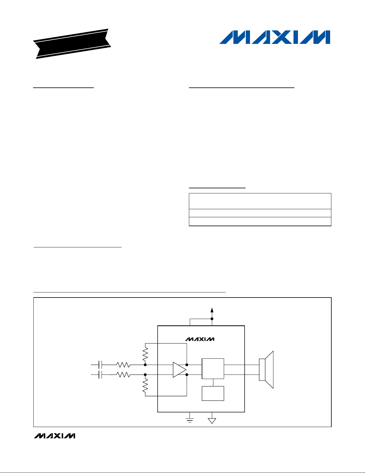
Simplified Block Diagram
19-0701; Rev 0; 12/06
For pricing, delivery, and ordering information, please contact Maxim/Dallas Direct! at
1-888-629-4642, or visit Maxim’s website at www.maxim-ic.com.
EVALUATION KIT
AVAILABLE
MP3 Players
Personal Media Players
Handheld Gaming
Consoles
Cell Phones
Smartphones
Notebook Computers
Applications
Typical Application Circuit/Functional Diagram and Pin
Configurations appear at end of data sheet.
UCSP is a trademark of Maxim Integrated Products, Inc.
+
Denotes lead-free package.
*
Future product—contact factory for availability.
**
EP = Exposed pad.
PART TEMP RANGE
MAX9730EBP+T* -40°C to +85°C 20 UCSP-20 B20-7
MAX9730ETI -40°C to +85°C 28 TQFN-EP** T2844-1
PINPACKAGE
PKG
CODE
Page 2
MAX9730
2.4W, Single-Supply, Class G Power Amplifier
2 _______________________________________________________________________________________
ABSOLUTE MAXIMUM RATINGS
ELECTRICAL CHARACTERISTICS
(VCC= CPVDD= SHDN = 3.6V, GND = CPGND = 0V, R
IN+
= R
IN-
= 10kΩ, R
FB+
= R
FB-
= 10kΩ, RFS= 100kΩ, C1 = 4.7µF, C2 =
10µF; speaker load resistors (R
L
) are terminated between OUT+ and OUT-, unless otherwise stated; TA= T
MIN
to T
MAX
, unless other-
wise noted. Typical values are at T
A
= +25°C.) (Notes 1, 2)
Stresses beyond those listed under “Absolute Maximum Ratings” may cause permanent damage to the device. These are stress ratings only, and functional
operation of the device at these or any other conditions beyond those indicated in the operational sections of the specifications is not implied. Exposure to
absolute maximum rating conditions for extended periods may affect device reliability.
(Voltages with respect to GND.)
V
CC
, CPVDD.............................................................-0.3V to +6V
PV
SS
, SVSS...............................................................-6V to +0.3V
CPGND..................................................................-0.3V to +0.3V
OUT+, OUT-...................................(SV
SS
- 0.3V) to (VCC+ 0.3V)
IN+, IN-, FB+, FB- ......................................-0.3V to (V
CC
+ 0.3V)
C1N..........................................(PV
SS
- 0.3V) to (CPGND + 0.3V)
C1P.......................................(CPGND - 0.3V) to (CPV
DD
+ 0.3V)
FS, SHDN ...................................................-0.3V to (V
CC
+ 0.3V)
Continuous Current Into/Out of
OUT+, OUT-, V
CC
, GND, SVSS.....................................800mA
CPV
DD
, CPGND, C1P, C1N, PVSS.................................800mA
Any Other Pin ..................................................................20mA
Duration of OUT+, OUT- Short Circuit to
V
CC
, GND, CPVDD, CPGND ..................................Continuous
Continuous Power Dissipation (T
A
= +70°C)
20-Bump UCSP (derate 10.3mW/°C above +70°C) .....827mW
28-Pin TQFN (derate 20.8mW/°C above +70°C) ........1667mW
Operating Temperature Range ...........................-40°C to +85°C
Storage Temperature Range .............................-65°C to +150°C
Lead Temperature (soldering, 10s) ................................+300°C
Bump Temperature (soldering) Reflow............................+235°C
PARAMETER SYMBOL CONDITIONS MIN TYP MAX UNITS
GENERAL
Supply Voltage Range V
Quiescent Current I
Chip Power Dissipation P
Shutdown Current I
Turn-On Time t
Input DC Bias Voltage V
Charge-Pump Oscillator
Frequency (Slow Mode)
Maximum Capacitive Load C
CC
CC
DISS
SHDN
ON
BIAS
f
OSC
L
SHDN Input Threshold (Note 3)
SHDN Input Leakage Current ±1 µA
SPEAKER AMPLIFIER
Output Offset Voltage V
OS
Common-Mode Rejection Ratio CMRR fIN = 1kHz (Note 4) 68 dB
Click-and-Pop Level V
CP
Inferred from PSRR test 2.7 5.5 V
V
= 2.8V
OUT
SHDN = GND 0.3 5 µA
Time from shutdown or power-on to full
operation
IN_ inputs 1.1 1.24 1.4 V
I
= 0mA (slow mode) 55 83 110
LOAD
I
> 100mA (normal mode) 230 330 430
LOAD
V
IH
V
IL
TA = +25°C ±3 ±15
T
≤ TA ≤ T
MIN
Peak voltage into/out of shutdown
A-weighted, 32 samples per second
(Notes 5, 6)
812mA
, f = 1kHz, RL = 8Ω 0.9 W
RMS
50 ms
200 pF
1.4
MAX
-52 dBV
0.4
±20
kHz
V
mV
Page 3
MAX9730
2.4W, Single-Supply, Class G Power Amplifier
_______________________________________________________________________________________ 3
ELECTRICAL CHARACTERISTICS (continued)
(VCC= CPVDD= SHDN = 3.6V, GND = CPGND = 0V, R
IN+
= R
IN-
= 10kΩ, R
FB+
= R
FB-
= 10kΩ, RFS= 100kΩ, C1 = 4.7µF, C2 =
10µF; speaker load resistors (R
L
) are terminated between OUT+ and OUT-, unless otherwise stated; TA= T
MIN
to T
MAX
, unless other-
wise noted. Typical values are at T
A
= +25°C.) (Notes 1, 2)
Note 1: All devices are 100% production tested at room temperature. All temperature limits are guaranteed by design.
Note 2: Testing performed with resistive and inductive loads to simulate an actual speaker load. For dynamic speakers,
R
L
= 8Ω, 68µH.
Note 3: Designed for 1.8V logic.
Note 4: R
IN_
and R
FB_
have 0.5% tolerance.
Note 5: Amplifier inputs AC-coupled to GND.
Note 6: Testing performed at room temperature with 8Ω resistive load in series with 68µH inductive load connected across BTL
output for speaker amplifier. Mode transitions are controlled by SHDN. V
CP
is the peak output transient expressed in dBV.
Note 7: Voltage gain is defined as: [V
OUT+
- V
OUT-
] / [V
IN+
- V
IN-
].
Note 8: Mode A tone burst tested at full amplitude for one cycle and half amplitude for nine cycles. Mode B tone burst tested at
full amplitude for three cycles and half amplitude for seven cycles. Full amplitude is defined as 1% THD+N at full battery
(V
CC
= 4.2V).
Electrical Characteristics
table targets must be met at THD+N = 1% for one cycle (Mode A) and THD+N <
5% for three cycles (Mode B).
Note 9: Dynamic range is calculated by measuring the RMS voltage difference between a -60dBFS output signal and the noise
floor, then adding 60dB. Full scale is defined as the output signal needed to achieve 1% THD+N.
PARAMETER SYMBOL CONDITIONS MIN TYP MAX UNITS
Voltage Gain A
Continuous Output Power P
(Notes 4, 7) 11.5 12 12.5 dB
V
OUT
THD+N = 1%, f = 1kHz,
R
f = 1kHz, 1% THD+N,
Z
Output Voltage V
OUT
f = 10kHz, 1% THD+N,
Z
load
VCC = 2.7V to 5.5V 63 77
Power-Supply Rejection Ratio
(Note 4)
PSRR
f = 217Hz, 200mV
f = 1kHz, 200mV
f = 20kHz, 200mV
Total Harmonic Distortion Plus
Noise
THD+N
Signal-to-Noise Ratio SNR
RL = 8Ω, V
R
V
A-weighted
Dynamic Range DR (Note 9)
= 8Ω
L
= 1µF + 10Ω
L
= 1µF + 10Ω, no
L
= 1kHz / 400mW 0.007
OUT
= 8Ω, V
L
= 0.5W, inputs to GND by C1N,
OUT
= 1kHz / 1W 0.12
OUT
VCC = 5V 2.4
VCC = 4.2V 1.67
VCC = 3.6V 1.25
V
= 3.0V 0.8
CC
VCC = 5V 7.1
VCC = 4.2V 5.9
VCC = 3.6V 5.1
V
= 3.0V 4.2
CC
VCC = 5V 6.5
VCC = 4.2V 5.4
VCC = 3.6V 4.7
= 3.0V 3.8
V
CC
ripple 77
P-P
ripple 77
P-P
ripple 58
P-P
22Hz to 22kHz 96
A-weighted 99
95 dB
V
RMS
W
dB
%
dB
Page 4
MAX9730
2.4W, Single-Supply, Class G Power Amplifier
4 _______________________________________________________________________________________
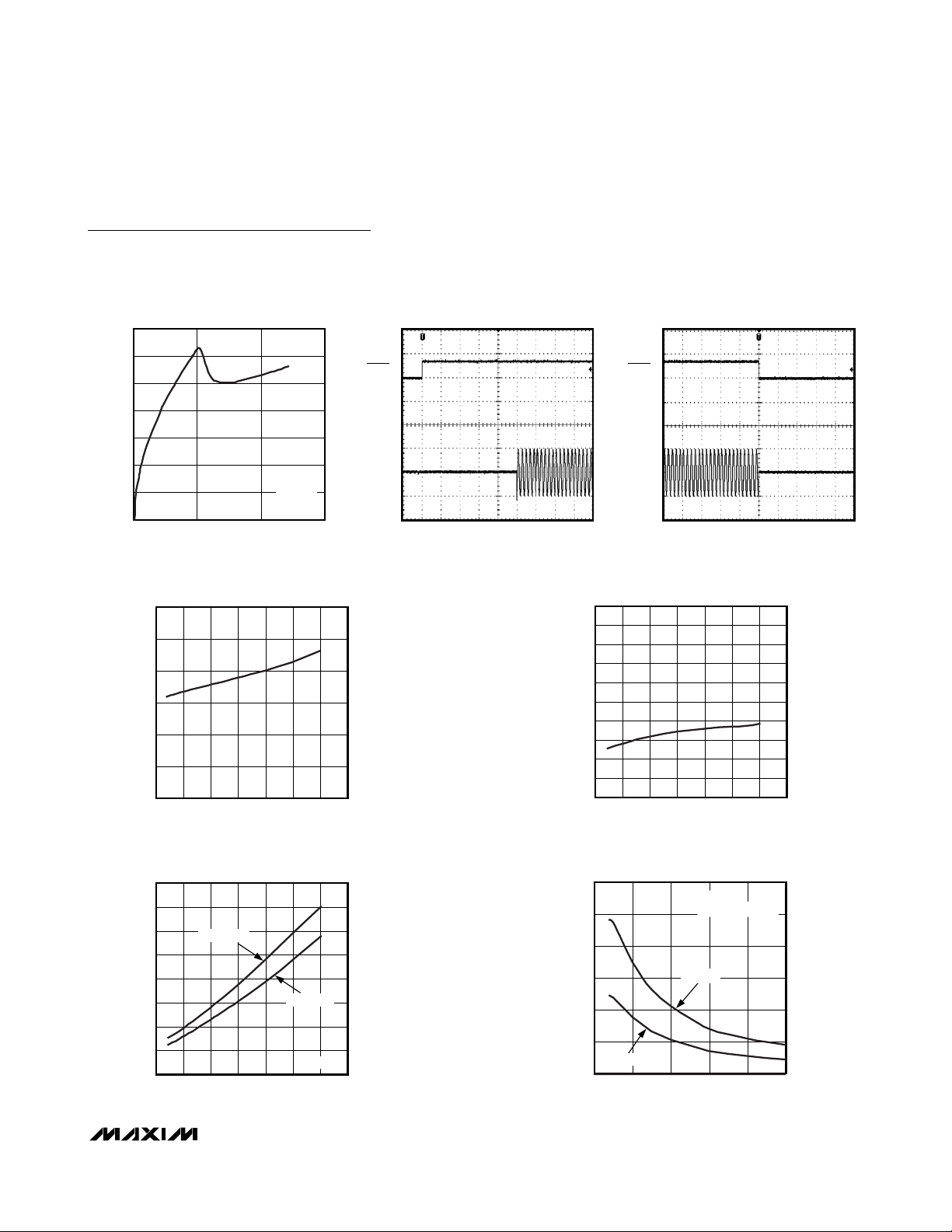
Typical Operating Characteristics
(VCC= CPVDD= SHDN = 3.6V, GND = CPGND = 0V, R
IN+
= R
IN-
= 10kΩ, R
FB+
= R
FB-
= 10kΩ, RFS= 100kΩ, C1 = 4.7µF, C2 =
10µF, R
L
= 8Ω; speaker load resistors (RL) are terminated between OUT+ and OUT-, unless otherwise stated; TA= T
MIN
to T
MAX
,
unless otherwise noted. Typical values are at TA= +25°C.) (Notes 1, 2)
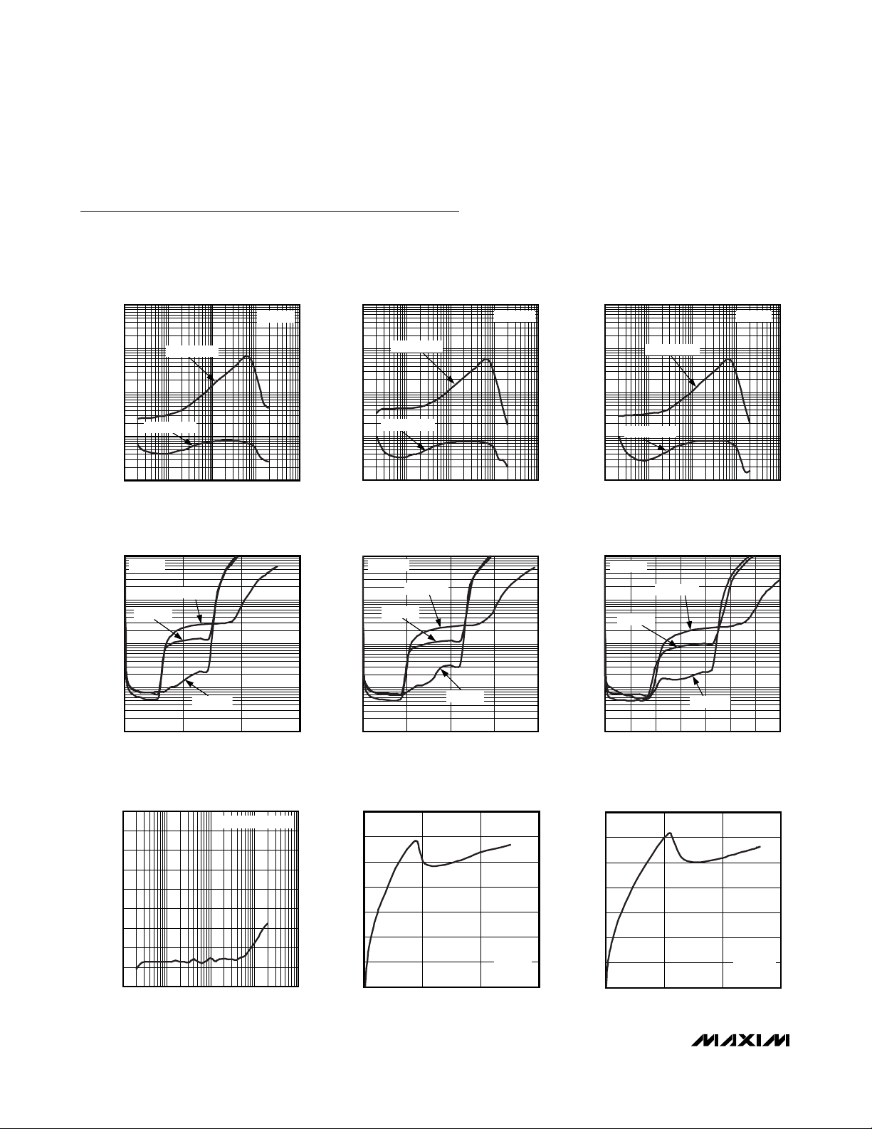
TOTAL HARMONIC DISTORTION PLUS
NOISE vs. FREQUENCY
MAX9730 toc01
FREQUENCY (kHz)
THD+N (%)
1010.1
0.01
0.1
1
10
0.001
0.01 100
V
CC
= 3V
P
OUT
= 0.69W
P
OUT
= 0.33W
TOTAL HARMONIC DISTORTION PLUS
NOISE vs. FREQUENCY
MAX9730 toc02
FREQUENCY (kHz)
THD+N (%)
1010.1
0.01
0.1
1
10
0.001
0.01 100
V
CC
= 3.6V
P
OUT
= 0.37W
P
OUT
= 0.93W
TOTAL HARMONIC DISTORTION PLUS
NOISE vs. FREQUENCY
MAX9730 toc03
FREQUENCY (kHz)
THD+N (%)
1010.1
0.01
0.1
1
10
0.001
0.01 100
V
CC
= 5V
P
OUT
= 0.83W
P
OUT
= 2.08W
TOTAL HARMONIC DISTORTION PLUS
NOISE vs. OUTPUT POWER
MAX9730 toc04
OUTPUT POWER (W)
THD+N (%)
1.00.5
0.01
0.1
1
10
0.001
0 1.5
V
CC
= 3V
f
IN
= 1kHz
f
IN
= 10kHz
f
IN
= 20Hz
TOTAL HARMONIC DISTORTION PLUS
NOISE vs. OUTPUT POWER
MAX9730 toc05
OUTPUT POWER (W)
THD+N (%)
1.51.00.5
0.01
0.1
1
10
0.001
0 2.0
V
CC
= 3.6V
f
IN
= 1kHz
f
IN
= 10kHz
f
IN
= 20Hz
TOTAL HARMONIC DISTORTION PLUS
NOISE vs. OUTPUT POWER
MAX9730 toc06
OUTPUT POWER (W)
THD+N (%)
3.02.52.01.51.00.5
0.01
0.1
1
10
0.001
03.5
f
IN
= 20Hz
f
IN
= 10kHz
f
IN
= 1kHz
V
CC
= 5V
POWER-SUPPLY REJECTION RATIO
vs. FREQUENCY
MAX9730 toc07
FREQUENCY (kHz)
PSRR (dB)
1010.1
-80
-70
-60
-50
-40
-30
-20
-10
0
-90
0.01 100
V
RIPPLE
= 200mV
P-P
POWER EFFICIENCY
vs. OUTPUT POWER
MAX9730 toc08
OUTPUT POWER (W)
EFFICIENCY (%)
1.00.5
10
20
30
40
50
60
70
0
01.5
V
CC
= 3V
f
IN
= 1kHz
POWER EFFICIENCY
vs. OUTPUT POWER
MAX9730 toc09
OUTPUT POWER (W)
EFFICIENCY (%)
1.00.5
10
20
30
40
50
60
70
0
01.5
V
CC
= 3.6V
f
IN
= 1kHz
Page 5
Typical Operating Characteristics (continued)
(VCC= CPVDD= SHDN = 3.6V, GND = CPGND = 0V, R
IN+
= R
IN-
= 10kΩ, R
FB+
= R
FB-
= 10kΩ, RFS= 100kΩ, C1 = 4.7µF, C2 =
10µF, R
L
= 8Ω; speaker load resistors (RL) are terminated between OUT+ and OUT-, unless otherwise stated; TA= T
MIN
to T
MAX
,
unless otherwise noted. Typical values are at TA= +25°C.) (Notes 1, 2)
MAX9730
2.4W, Single-Supply, Class G Power Amplifier
_______________________________________________________________________________________
5
POWER EFFICIENCY
vs. OUTPUT POWER
70
60
50
40
30
EFFICIENCY (%)
20
10
0
03
OUTPUT POWER (W)
V
CC
f
IN
21
= 5V
= 1kHz
MAX9730 toc10
OUT+ - OUT-
500mV/div
SHDN
5V/div
SUPPLY CURRENT
vs. SUPPLY VOLTAGE
12
10
8
6
4
SUPPLY CURRENT (mA)
2
0
2.5 6.0
SUPPLY VOLTAGE (V)
MAX9730 toc13
5.55.04.54.03.53.0
OUTPUT POWER
vs. SUPPLY VOLTAGE
4.0
3.5
3.0
2.5
2.0
1.5
OUTPUT POWER (W)
1.0
0.5
0
2.5 6.0
10% THD+N
SUPPLY VOLTAGE (V)
1% THD+N
f
IN
MAX9730 toc15
= 1kHz
5.55.03.0 3.5 4.0 4.5
STARTUP WAVEFORM
10ms/div
MAX9730 toc11
SHDN
5V/div
OUT+ - OUT-
500mV/div
SHUTDOWN WAVEFORM
SHUTDOWN CURRENT
vs. SUPPLY VOLTAGE
1.0
0.9
0.8
0.7
0.6
0.5
0.4
0.3
SHUTDOWN CURRENT (μA)
0.2
0.1
0
2.5 6.0
SUPPLY VOLTAGE (V)
OUTPUT POWER
vs. LOAD RESISTANCE
3.0
2.5
2.0
1.5
1.0
OUTPUT POWER (W)
0.5
V
= 3.6V
CC
0
0100
LOAD RESISTANCE (Ω)
f
= 1kHz
IN
P
OUT
V
= 5V
CC
10ms/div
5.55.04.0 4.53.53.0
AT 1% THD+N
80604020
MAX9730 toc14
MAX9730 toc16
MAX9730 toc12
Page 6

MAX9730
2.4W, Single-Supply, Class G Power Amplifier
6 _______________________________________________________________________________________
6 _______________________________________________________________________________________
Pin Description
Typical Operating Characteristics (continued)
(VCC= CPVDD= SHDN = 3.6V, GND = CPGND = 0V, R
IN+
= R
IN-
= 10kΩ, R
FB+
= R
FB-
= 10kΩ, RFS= 100kΩ, C1 = 4.7µF, C2 =
10µF, R
L
= 8Ω; speaker load resistors (RL) are terminated between OUT+ and OUT-, unless otherwise stated; TA= T
MIN
to T
MAX
,
unless otherwise noted. Typical values are at TA= +25°C.) (Notes 1, 2)
OUT+
5V/div
OUT-
5V/div
OUT+ - OUT-
10V/div
CLASS G OUTPUT WAVEFORM
200μs/div
MAX9730 toc17
1% THD+N
20
18
16
14
12
10
GAIN (dB)
8
6
4
2
0
FREQUENCY RESPONSE
10 100k
FREQUENCY (Hz)
10k1k100
P
OUT
= 1W
MAX9730 toc18
PIN
TQFN UCSP
NAME FUNCTION
1B2SHDN Shutdown
2, 5, 6, 8, 11, 17,
19, 23, 25, 28
3 A2 C1P
4 A3 CPV
— N.C. No Connection. No internal connection.
Charge-Pump Flying Capacitor, Positive Terminal. Connect a 4.7µF
capacitor between C1P and C1N.
DD
Charge-Pump Positive Supply
7 A4 FB- Negative Amplifier Feedback
9 A5 IN- Negative Amplifier Input
10 B5 IN+ Positive Amplifier Input
12 B4 FB+ Positive Amplifier Feedback
13 C5 FS
14, 22 D1, D5 V
15, 21 C2, C4 SV
CC
SS
Charge-Pump Frequency Set. Connect a 100kΩ resistor from FS to
GND to set the charge-pump switching frequency.
Supply Voltage. Bypass with a 10µF capacitor to GND.
Amplifier Negative Power Supply. Connect to PVSS.
16 D4 OUT- Negative Amplifier Output
18 D3 GND Ground
20 D2 OUT+ Positive Amplifier Output
24 C1 PV
26 B1 C1N
SS
Charge-Pump Output. Connect a 10µF capacitor between PVSS and
CPGND.
Charge-Pump Flying Capacitor, Negative Terminal. Connect a 4.7µF
capacitor between C1N and C1P.
27 A1 CPGND Charge-Pump Ground. Connect to GND.
EP — EP Exposed Pad. Connect the TQFN EP to GND.
Page 7

MAX9730
2.4W, Single-Supply, Class G Power Amplifier
_______________________________________________________________________________________ 7
Detailed Description
The MAX9730 Class G power amplifier with inverting
charge pump is the latest in linear amplifier technology. The Class G output stage offers the performance
of a Class AB amplifier while increasing efficiency to
extend battery life. The integrated inverting charge
pump generates a negative supply capable of delivering up to 500mA.
The Class G output stage and the inverting charge pump
allow the MAX9730 to deliver an output power that is up
to four times greater than a traditional single-supply linear
amplifier. This allows the MAX9730 to maintain 0.8W into
an 8Ω load as the battery rail collapses.
Class G Operation and Efficiency
The MAX9730 Class G amplifier is a linear amplifier that
operates within a low (VCCto GND) and high (VCCto
SV
SS
) supply range. Figure 1 illustrates the transition
from the low to high supply range. For small signals,
the device operates within the lower (V
CC
to GND) sup-
ply range. In this range, the operation of the device is
identical to a traditional single-supply Class AB amplifier where:
I
LOAD
= I
N1
As the output signal increases, so a wider supply is
needed, the device begins its transition to the higher supply range (V
CC
to SVSS) for the large signals. To ensure a
seamless transition between the low and high supply
ranges, both of the lower transistors are on so that:
I
LOAD
= I
N1
+ I
N2
As the output signal continues to increase, the transition to the high supply is complete. The device then
operates in the higher supply range, where the operation of the device is identical to a traditional dual-supply Class AB amplifier where:
I
LOAD
= I
N2
During operation, the output common-mode voltage of
the MAX9730 adjusts dynamically as the device transitions between supply ranges.
Figure 1. Class G Supply Transition
V
CC
BTL CLASS G SUPPLY TRANSITION
V
CC
V
CC
I
P
ON
P
LOW SUPPLY RANGE OPERATION
R
L
I
N1
SV
SS
= I
I
P
N1
I
P
ON
P
N1
ON
N2
OFF
R
L
SV
SS
SUPPLY TRANSITION
= IN1 + I
I
P
N2
I
N1
N1
I
N2
N2
ON P
ON
ON
I
P
R
L
I
N2
SV
SS
HIGH SUPPLY RANGE OPERATION
= I
I
P
N2
N1
OFF
N2
ON
Page 8
MAX9730
2.4W, Single-Supply, Class G Power Amplifier
8 _______________________________________________________________________________________
Utilizing a Class G output stage with an inverting
charge pump allows the MAX9730 to realize a 2.4W
output power with a 5V supply.
The theoretical best efficiency of a linear amplifier is
78%; however, that efficiency is only exhibited at peak
output powers. Under normal operating levels (typical
music reproduction levels), efficiency falls below 30%,
whereas the MAX9730 still exhibits 50% efficiency
under the same conditions.
Inverting Charge Pump
The MAX9730 features an integrated charge pump with
an inverted supply rail that can supply greater than
700mA over the positive 2.7V to 5.5V supply range. In
the case of the MAX9730, the charge pump generates
the negative supply rail (PV
SS
) needed to create the
higher supply range, which allows the output of the
device to operate over a greater dynamic range as the
battery supply collapses over time.
Shutdown Mode
The MAX9730 has a shutdown mode that reduces
power consumption and extends battery life. Driving
SHDN low places the MAX9730 in a low-power (0.3µA)
shutdown mode. Connect SHDN to VCCfor normal
operation.
Click-and-Pop Suppression
The MAX9730 Class G amplifier features Maxim’s comprehensive, industry-leading click-and-pop suppression. During startup, the click-and-pop suppression
circuitry eliminates any audible transient sources internal to the device.
Applications Information
Differential Input Amplifier
The MAX9730 features a differential input configuration,
making the device compatible with many CODECs, and
offering improved noise immunity over a single-ended
input amplifier. In devices such as PCs, noisy digital
signals can be picked up by the amplifier’s input
traces. The signals appear at the amplifiers’ inputs as
common-mode noise. A differential input amplifier
amplifies the difference of the two inputs, and signals
common to both inputs are canceled out. When configured for differential inputs, the voltage gain of the
MAX9730 is set by:
where A
V
is the desired voltage gain in dB. R
IN+
should
be equal to R
IN-
and R
FB+
should be equal to R
FB-
. The
Class G output stage has a fixed gain of 4V/V (12dB). Any
gain or attenuation set by the external input stage resistors
will add to or subtract from this fixed gain. See Figure 3.
Figure 2. MAX9730 Efficiency vs. Class AB Efficiency vs.
Class D Efficiency
Figure 3. Gain Setting
A
=×
V
⎡
⎛
⎞
R
FB
⎢
20 4log
⎢
⎣
_
⎜
⎟
R
⎝
⎠
IN
_
⎤
⎥
dB
()
⎥
⎦
MAX9730
100
90
80
70
60
50
40
EFFICIENCY (%)
30
20
10
0
EFFICIENCY vs. CLASS AB
MAX9730
TRADITIONAL CLASS AB
0 2.0
OUTPUT POWER (W)
1.51.00.5
MAX9730 fig02
C
IN-
R
IN+
R
C
IN-
IN-
FB+
R
FB+
IN+
+
IN-
-
R
FB-
FB-
MAX9730
CLASS G
OUTPUT
STAGE
Page 9

MAX9730
2.4W, Single-Supply, Class G Power Amplifier
_______________________________________________________________________________________ 9
In differential input configurations, the common-mode
rejection ratio (CMRR) is primarily limited by the external resistor and capacitor matching. Ideally, to achieve
the highest possible CMRR, the following external components should be selected where:
and
Component Selection
Input-Coupling Capacitor
The AC-coupling capacitors (C
IN_
) and input resistors
(R
IN_
) form highpass filters that remove any DC bias from
an input signal (see the
Typical Application
Circuit/Functional Diagram
). C
IN_
blocks DC voltages
from the amplifier. The -3dB point of the highpass filter,
assuming zero source impedance due to the input signal
source, is given by:
Choose CINso that f
-3dB
is well below the lowest fre-
quency of interest. Setting f
-3dB
too high affects the
amplifier’s low frequency response. Use capacitors with
low-voltage coefficient dielectrics. Aluminum electrolytic,
tantalum, or film dielectric capacitors are good choices
for AC-coupling capacitors. Capacitors with high-voltage
coefficients, such as ceramics (non-C0G dielectrics),
can result in increased distortion at low frequencies.
Charge-Pump Capacitor Selection
Use capacitors with an ESR less than 50mΩ for optimum performance. Low-ESR ceramic capacitors minimize the output resistance of the charge pump. For
best performance over the extended temperature
range, select capacitors with an X7R dielectric.
Flying Capacitor (C1)
The value of the flying capacitor (C1) affects the load
regulation and output resistance of the charge pump. A
C1 value that is too small degrades the device’s ability
to provide sufficient current drive. Increasing the value
of C1 improves load regulation and reduces the chargepump output resistance to an extent. Above 1µF, the onresistance of the switches and the ESR of C1 and C2
dominate. A 4.7µF capacitor is recommended.
Hold Capacitor (C2)
The output capacitor value and ESR directly affect the
ripple at PVSS. Increasing C2 reduces output ripple.
Likewise, decreasing the ESR of C2 reduces both ripple and output resistance. A 10µF capacitor is recommended.
Charge-Pump Frequency Set Resistor (RFS)
The charge pump operates in two modes. When the
charge pump is loaded below 100mA, it operates in a
slow mode where the oscillation frequency is reduced
to 1/4 of its normal operating frequency. Once loaded,
the charge-pump oscillation frequency returns to normal operation. In applications where the design may be
sensitive to the operating charge-pump oscillation frequency, the value of the external resistor RFScan be
changed to adjust the charge-pump oscillation frequency (see Figure 4).
Figure 4. Charge-Pump Oscillation Frequency vs. R
FS
R
R
FB
IN
R
FB
+
+
−
=
R
IN
−
CC
=
IN IN+
−
f
=
dB
−
3
2π
1
RC
××
IN IN
__
Hz
()
CHARGE-PUMP OSCILLATION
FREQUENCY vs. R
600
550
500
450
400
350
300
250
CHARGE-PUMP OSCILLATION FREQUENCY (kHz)
200
50 150
RFS (kΩ)
I
LOAD
FS
> 100mA
MAX9730 fig04
12510075
Page 10

MAX9730
Thermal Considerations
Class G amplifiers provide much better efficiency and
thermal performance than a comparable Class AB
amplifier. However, the system’s thermal performance
must be considered with realistic expectations and
include consideration of many parameters. This section
examines Class G amplifiers using general examples to
illustrate good design practices.
TQFN Considerations
The exposed pad is the primary route of keeping heat
away from the IC. With a bottom-side exposed pad, the
PCB and its copper become the primary heatsink for
the Class G amplifier. Solder the exposed pad to a
large copper polygon that is connected to the ground
plane.
The copper polygon to which the exposed pad is
attached should have multiple vias to the opposite side
of the PCB, where they connect to GND. Make this
polygon as large as possible within the system’s constraints.
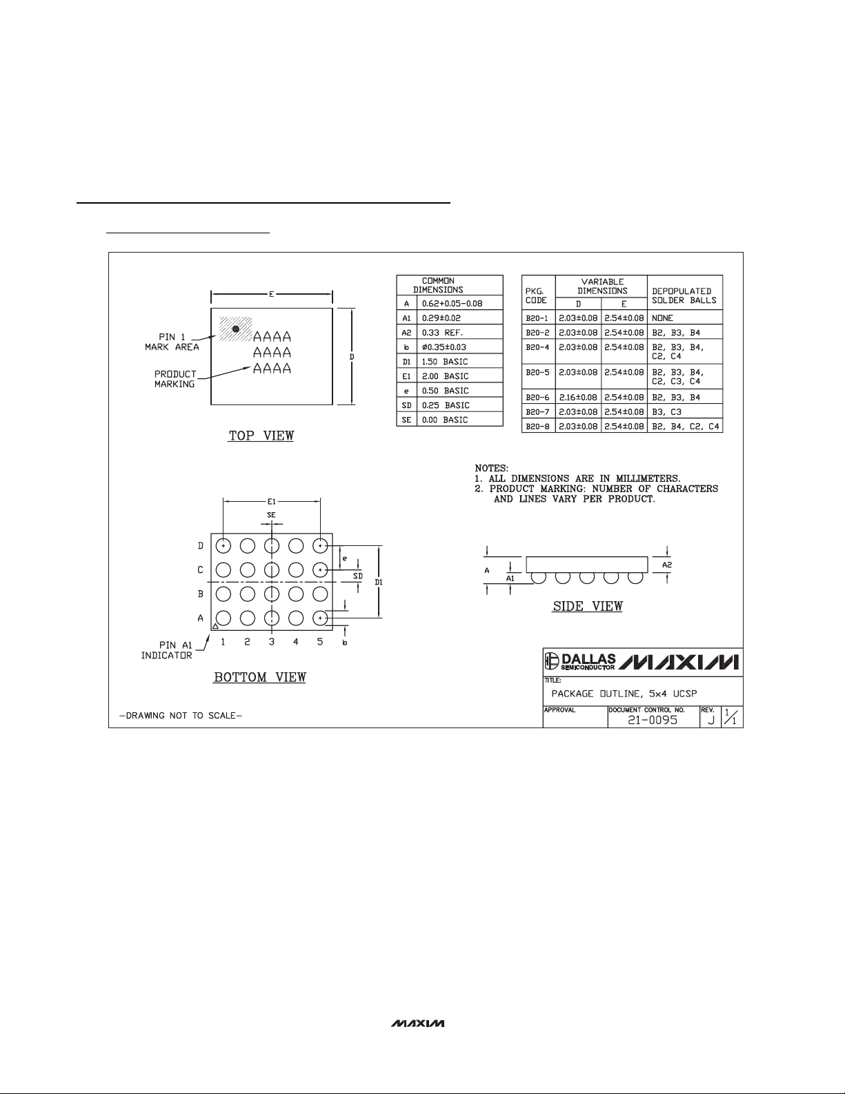
UCSP Applications Information
For the latest application details on UCSP construction,
dimensions, tape carrier information, PCB techniques,
bump-pad layout, and recommended reflow temperature profile, as well as the latest information on reliability
testing results, go to the Maxim website at www.maximic.com/ucsp for the application note,
UCSP—A Wafer-
Level Chip-Scale Package
.
2.4W, Single-Supply, Class G Power Amplifier
10 ______________________________________________________________________________________
Typical Application Circuit/Functional Diagram
V
DD
12 (B4)
C
IN
1μF
C
IN
1μF
( ) UCSP PACKAGE
DEVICE SHOWN WITH A
*SYSTEM-LEVEL REQUIREMENT TYPICALLY 10μF
R
10kΩ
R
10kΩ
IN-
IN-
= 12dB
V
R
10kΩ
R
10kΩ
FB+
10 (B5)
9 (A5)
FB-
7 (A4)
18 (D3) 27 (A1) 26 (B1) 3 (A2)
14, 22
(D1, D5)
1 (B2)
V
SHDN
FB+
CC
MAX9730
IN+
+
IN-
FB-
-
GND
CPGND PV
C1N
CPV
4.7μF
4 (A3)
DD
CLASS G
OUTPUT
STAGE
CHARGE
PUMP
C1
C1P
0.1μF
SS
24 (C1)
*
OUT+
OUT-
SV
15, 21
(C2, C4)
20 (D2)
16 (D4)
13 (C5)
FS
R
FS
SS
100kΩ
C2
10μF
Page 11

MAX9730
2.4W, Single-Supply, Class G Power Amplifier
______________________________________________________________________________________ 11
Pin Configurations
Chip Information
PROCESS: BiCMOS
TOP VIEW
SHDN
1
2
N.C.
3
C1P
CPV
4
DD
5
N.C.
6
N.C.
FB-
7
*EXPOSED PAD.
TOP VIEW
(BUMP SIDE DOWN)
N.C.
CPGND
C1N
28
27
+
26
N.C.
25
SS
PV
24
MAX9730
EP*
8
9
10
11
12
IN-
N.C.
IN+
N.C.
FB+
THIN QFN
N.C.
23
13
FS
CC
V
22
SV
21
SS
20
OUT+
19
N.C.
18
GND
17
N.C.
16
OUT-
SV
15
SS
14
CC
V
A
B
C
D
1
CPGND
C1N
PV
SS
V
CC
MAX9730
FB-
FB+
SV
OUT-
4
IN-
IN+
FS
SS
V
CC
23 5
CPV
C1P
SHDN
SV
OUT+
SS
DD
GND
UCSP
Page 12

MAX9730
2.4W, Single-Supply, Class G Power Amplifier
12 ______________________________________________________________________________________
Package Information
(The package drawing(s) in this data sheet may not reflect the most current specifications. For the latest package outline information
go to www.maxim-ic.com/packages
.)
24L QFN THIN.EPS
PACKAGE OUTLINE,
12, 16, 20, 24, 28L THIN QFN, 4x4x0.8mm
21-0139
1
E
2
Page 13

MAX9730
2.4W, Single-Supply, Class G Power Amplifier
______________________________________________________________________________________ 13
Package Information (continued)
(The package drawing(s) in this data sheet may not reflect the most current specifications. For the latest package outline information
go to www.maxim-ic.com/packages
.)
PACKAGE OUTLINE,
12, 16, 20, 24, 28L THIN QFN, 4x4x0.8mm
21-0139
2
E
2
Page 14
MAX9730
2.4W, Single-Supply, Class G Power Amplifier
Maxim cannot assume responsibility for use of any circuitry other than circuitry entirely embodied in a Maxim product. No circuit patent licenses are
implied. Maxim reserves the right to change the circuitry and specifications without notice at any time.
14
____________________Maxim Integrated Products, 120 San Gabriel Drive, Sunnyvale, CA 94086 408-737-7600
© 2006 Maxim Integrated Products is a registered trademark of Maxim Integrated Products, Inc.
Package Information (continued)
(The package drawing(s) in this data sheet may not reflect the most current specifications. For the latest package outline information
go to www.maxim-ic.com/packages
.)
5x4 UCSP.EPS
 Loading...