

Page 1
General Description
The MAX9729 stereo DirectDrive™ headphone amplifier features bass boost, volume control, an input mux,
and an I2C/SMBus™-compatible serial interface. This
makes the MAX9729 ideal for portable audio applications where space is at a premium and performance is
essential. The MAX9729 operates from a single 1.8V to
3.6V, and uses Maxim’s patented
†
DirectDrive architecture, eliminating the need for large DC-blocking capacitors. The headphone amplifiers deliver 52mW into a
32Ω load, feature low 0.03% THD+N, and high 90dB
PSRR. Maxim’s industry-leading click-and-pop suppression circuitry reduces audible transients during
power and shutdown cycles.
The BassMax feature boosts the bass response of the
amplifier, improving audio reproduction for low-end
headphones. The integrated volume control features 32
discrete volume levels along with a ramping function to
ensure smooth transitions during shutdown cycles and
input selection. The MAX9729’s eight programmable
maximum gain settings allow for a wide range of input
signal levels. A 3:1 multiplexer/mixer allows the selection
and summation of multiple stereo input signal sources.
The MAX9729 also includes a dedicated BEEP input
with independent attenuation control. BassMax, volume
control, gain settings, and input selection are controlled
using the I2C/SMBus-compatible serial interface. A lowpower, 5µA shutdown mode is controlled through an
external logic input or the serial interface.
The MAX9729 consumes only 4.8mA of supply current,
provides short-circuit and thermal-overload protection,
and is specified over the -40°C to +85°C extended temperature range. The MAX9729 is available in a spacesaving 28-pin thin QFN package (5mm x 5mm x 0.8mm).
Features
♦ DirectDrive Headphone Amplifier Eliminates
Bulky DC-Blocking Capacitors
♦ 3:1 Input Multiplexer with Digital-Fade Circuitry
♦ Software-Enabled Bass Boost
♦ 32-Step Integrated Volume Control
♦ Beep Input with Programmable Output Level
♦ Low Quiescent Current
♦ Industry-Leading Click-and-Pop Suppression
♦ I2C-Compatible 2-Wire Interface
♦ Short-Circuit Protection
♦ 1.8V to 3.6V Single-Supply Operation
♦ Available in Space-Saving, Thermally Efficient
28-Pin TQFN-EP (5mm x 5mm x 0.8mm)
MAX9729
Stereo Headphone Amplifier with BassMax,
Volume Control, and Input Mux
________________________________________________________________
Maxim Integrated Products
1
19-0857; Rev 0; 7/07
For pricing, delivery, and ordering information, please contact Maxim Direct at 1-888-629-4642,
or visit Maxim’s website at www.maxim-ic.com.
EVALUATION KIT
AVAILABLE
Ordering Information
Note: This device is specified over the -40°C to +85°C operating
temperature range.
+
Denotes lead-free package.
*Last digit of slave address is pin programmable.
**EP = Exposed pad.
SMBus is a trademark of Intel Corp.
†
U.S. Patent # 7,061,327
Pin Configuration appears at end of data sheet.
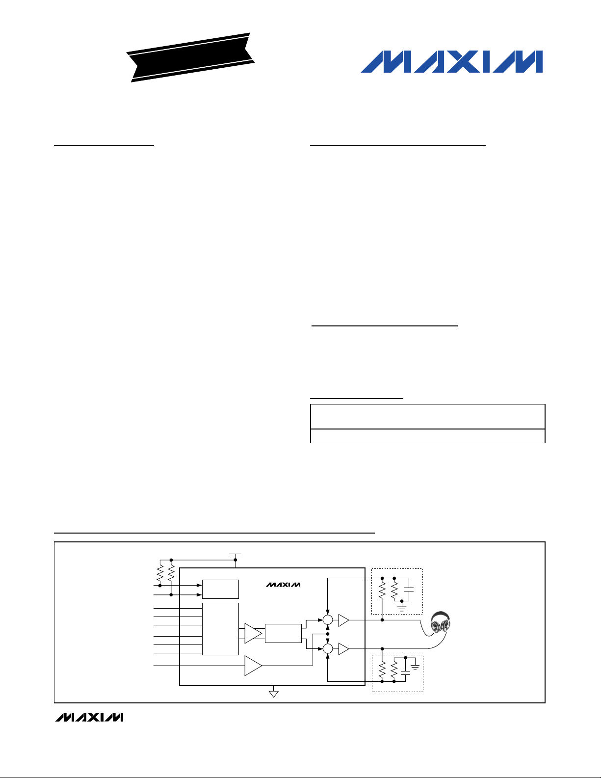
I2C INTERFACE
MUX
MIXER
FADER
CONTROL
VOLUME
CONTROL
BassMax
BassMax
1.8V TO 3.6V
SCL
SDA
INL1
INL2
INL3
INR1
INR2
INR3
BEEP
OUTL
BML
BMR
MAX9729
Σ
Σ
PGA
OUTR
PGA
Simplified Block Diagram
Portable CD/DVD/MD
Players
Cell Phones
MP3/PMP Players
Automotive Rear Seat
Entertainment (RSE)
Flat-Panel TVs
Applications
PART
MAX9729ETI+ 28 TQFN-EP** 101000_ T2855-5
PINPACKAGE
SLAVE
ADDRESS*
PKG
CODE
Page 2
MAX9729
Stereo Headphone Amplifier with BassMax,
Volume Control, and Input Mux
2 _______________________________________________________________________________________
ABSOLUTE MAXIMUM RATINGS
ELECTRICAL CHARACTERISTICS (3V Supply)
(VDD= PVDD= SHDN = 3V, PGND = SGND = 0V, C1 = C2 = C3 = 1µF, BM_ = 0V, maximum gain setting = 6dB, volume attenuation
setting = -16dB (overall gain = -10dB), BassMax disabled. Load connected between OUT_ and PGND where specified. THD+N
measurement BW = 22Hz to 22kHz. T
A
= T
MIN
to T
MAX
, unless otherwise noted. Typical values are at TA= +25°C.) (Note 1)
Stresses beyond those listed under “Absolute Maximum Ratings” may cause permanent damage to the device. These are stress ratings only, and functional
operation of the device at these or any other conditions beyond those indicated in the operational sections of the specifications is not implied. Exposure to
absolute maximum rating conditions for extended periods may affect device reliability.
VDD, PVDDto PGND or SGND .................................-0.3V to +4V
V
DD
to PVDD................................................Internally Connected
PV
SS
to SVSS.......................................................................±0.3V
SGND to PGND...................................................................±0.3V
C1P to PGND..............................................-0.3V to (V
DD
+ 0.3V)
C1N to PGND............................................(PV
SS
- 0.3V) to +0.3V
PV
SS
, SVSSto PGND ................................................+0.3V to -4V
INL_, INR_, BEEP to SGND............(SV
SS
- 0.3V) to (VDD+ 0.3V)
SDA, SCL, BEEP_EN to PGND.................................-0.3V to +4V
SHDN to PGND ..........................................-0.3V to (V
DD
+ 0.3V)
OUT_ to PGND ............................................................-3V to +3V
BM_ to SGND ..............................................................-2V to +2V
Duration of OUT_ Short Circuit to PGND....................Continuous
Continuous Current Into/Out of:
V
DD
, C1P, C1N, PGND, PVSS, SVSS, or OUT_ .............±0.85A
All other pins.................................................................±20mA
Continuous Power Dissipation (T
A
= +70°C, multilayer board)
28-Pin Thin QFN (derate 28.6mW/°C above +70°C) 0.2286mW
Junction-to-Ambient Thermal Resistance (θ
JA
)
28-Pin TQFN.................................................................35°C/W
Operating Temperature Range ...........................-40°C to +85°C
Junction Temperature......................................................+150°C
Storage Temperature Range .............................-65°C to +150°C
OUT_ ESD Protection (Human Body Model) .......................±8kV
ESD Protection of All Other Pins ..........................................±2kV
Lead Temperature (soldering, 10s) .................................+300°C
PARAMETER SYMBOL CONDITIONS MIN TYP MAX UNITS
GENERAL
Supply Voltage Range V
Charge-Pump and Logic Supply
Voltage
Quiescent Supply Current I
Shutdown Supply Current I
Turn-On Time t
Beep Enable Time t
Thermal Shutdown Threshold T
Thermal Shutdown Hysteresis T
HEADPHONE AMPLIFIER
Input Resistance R
Output Offset Voltage V
BMR, BML Input Bias Current I
DD
PV
DD
DD
DD_SHDNVSHDN
ON
ON_BEEP
THRES
HYST
IN
OSHP
BIAS_BM
(Note 2) 1.8 3.6 V
(Note 2) 1.8 3.6 V
No load, BEEP_EN = VDD (Note 3) 5.5 8 mA
= 0V 5 10 µA
From shutdown mode to full operation 200 µs
Applicable to all maximum gain and
volume settings
Measured between OUT_ and SGND,
overall gain = -10dB (Note 3)
12 µs
146 °C
13 °C
14 25 35 kΩ
±0.7 ±3.5 mV
±10 ±100 nA
Page 3
MAX9729
Stereo Headphone Amplifier with BassMax,
Volume Control, and Input Mux
_______________________________________________________________________________________ 3
ELECTRICAL CHARACTERISTICS (3V Supply) (continued)
(VDD= PVDD= SHDN = 3V, PGND = SGND = 0V, C1 = C2 = C3 = 1µF, BM_ = 0V, maximum gain setting = 6dB, volume attenuation
setting = -16dB (overall gain = -10dB), BassMax disabled. Load connected between OUT_ and PGND where specified. THD+N
measurement BW = 22Hz to 22kHz. T
A
= T
MIN
to T
MAX
, unless otherwise noted. Typical values are at TA= +25°C.) (Note 1)
PARAMETER SYMBOL CONDITIONS MIN TYP MAX UNITS
Power-Supply Rejection Ratio
Output Power P
Total Harmonic Distortion Plus
Noise
Maximum Gain A
Beep Input Attenuation A
Signal-to-Noise Ratio SNR
Slew Rate SR 0.5 V/µs
Capacitive Drive No sustained oscillations 200 pF
Output Resistance in Shutdown R
PSRR (Note 3)
OUT
THD+N
VMAX
V_BEEP
OUT_SHDN
VDD = 1.8V to 3.6V, overall
gain = 6dB
f = 217Hz, 100mV
ripple, overall gain = 26dB
f = 1kHz, 100mV
overall gain = 26dB
f = 20kHz, 100mV
ripple, overall gain = 26dB
THD+N = 1%,
= 1kHz, overall
f
IN
gain = 1.8dB,
T
= +25°C (Note 4)
A
f
= 1kHz, overall
IN
gain = 3.5dB
(Note 4)
Register 0x01, B[2:0] = 000 3.5
Register 0x01, B[2:0] = 001 6
Register 0x01, B[2:0] = 010 8
Register 0x01, B[2:0] = 011 10
Register 0x01, B[2:0] = 100 19.5
Register 0x01, B[2:0] = 101 22
Register 0x01, B[2:0] = 110 24
Register 0x01, B[2:0] = 111 26
Register 0x01, B[7:5] = 000 10
Register 0x01, B[7:5] = 001 20
Register 0x01, B[7:5] = 010 30
Register 0x01, B[7:5] = 011 40
Register 0x01, B[7:5] = 100 50
Register 0x01, B[7:5] = 101 52
Register 0x01, B[7:5] = 110 54
Register 0x01, B[7:5] = 111 56
R
= 32Ω,
L
V
= 1V
OUT
= 0V, measured from OUT_ to
V
SHDN
SGND
BW = 22Hz to 22kHz 99
BW = 22Hz to 22kHz
RMS
and A-weighted
P-P
ripple,
P-P
P-P
RL = 16Ω 12 49
R
= 32Ω 21 52
L
RL = 16Ω ,
= 42m W
P
OU T
= 32Ω ,
R
L
P
= 40m W
OU T
72 95
90
82
58
0.04
0.04
101
20 kΩ
dB
mW
%
dB
dB
dB
Page 4
MAX9729
Stereo Headphone Amplifier with BassMax,
Volume Control, and Input Mux
4 _______________________________________________________________________________________
ELECTRICAL CHARACTERISTICS (3V Supply) (continued)
(VDD= PVDD= SHDN = 3V, PGND = SGND = 0V, C1 = C2 = C3 = 1µF, BM_ = 0V, maximum gain setting = 6dB, volume attenuation
setting = -16dB (overall gain = -10dB), BassMax disabled. Load connected between OUT_ and PGND where specified. THD+N
measurement BW = 22Hz to 22kHz. T
A
= T
MIN
to T
MAX
, unless otherwise noted. Typical values are at TA= +25°C.) (Note 1)
ELECTRICAL CHARACTERISTICS (2.4V Supply)
(VDD= PVDD= SHDN = 2.4V, PGND = SGND = 0V, C1 = C2 = C3 = 1µF, BM_ = 0V, maximum gain setting = 6dB, volume attenuation
setting = -16dB (overall gain = -10dB), BassMax disabled. Load connected between OUT_ and PGND where specified. THD+N
measurement BW = 22Hz to 22kHz. T
A
= T
MIN
to T
MAX
, unless otherwise noted. Typical values are at TA= +25°C.) (Note 1)
PARAMETER SYMBOL CONDITIONS MIN TYP MAX UNITS
Click-and-Pop Level K
Charge-Pump Switching Frequency f
Crosstalk
DIGITAL INPUTS (SHDN, SDA, SCL, BEEP_EN)
Input High Voltage V
Input Low Voltage V
Input Leakage Current -1 +1 µA
DIGITAL OUTPUTS (SDA)
Output Low Voltage V
Output High Current I
CP
CP
IH
IL
OL
OH
Peak voltage, Aweighted, 32 samples
per second
(Notes 3 and 5)
L to R, or R to L, f = 10kHz, V
1V
, RL = 32Ω, both channels loaded
RMS
IOL = 3mA 0.4 V
V
= V
SDA
DD
Into shutdown 81
Out of shutdown 80
505 600 730 kHz
=
OUT
1.4 V
78 dB
0.4 V
1µA
dBV
PARAMETER SYMBOL CONDITIONS MIN TYP MAX UNITS
Quiescent Current I
Shutdown Current I
Output Power P
Total Harmonic Distortion Plus
Noise
Power-Supply Rejection Ratio PSRR
DD
SHDN
OUT
THD+N
No load (Note 3) 4.5 mA
V
= 0V 4 µA
SHDN
THD+N = 1%,
f
= 1kHz, overall
IN
gain = 3.5dB,
T
= +25°C
A
(Note 4)
f
= 1kHz, overall
IN
gain = 3.5dB
(Note 4)
100mV
(Note 3)
P-P
ripple
RL = 16Ω 32
= 32Ω 32
R
L
RL = 16Ω ,
= 23m W
P
OU T
= 32Ω ,
R
L
= 23m W
P
OU T
f = 217Hz 90
f = 1kHz 85
f = 10kHz 61
0.03
0.03
mW
%
dB
Page 5
MAX9729
Stereo Headphone Amplifier with BassMax,
Volume Control, and Input Mux
_______________________________________________________________________________________ 5
TIMING CHARACTERISTICS
(VDD= PVDD= SHDN = 3V, PGND = SGND = 0V, C1 = C2 = C3 = 1µF, BM_ = 0V, maximum gain setting = 6dB, volume setting = -16dB
(overall gain = -10dB), BassMax disabled. Load connected between OUT_ and PGND where specified. T
A
= T
MIN
to T
MAX
, unless other-
wise noted. Typical values are at T
A
= +25°C.) (Notes 1 and 6)
ELECTRICAL CHARACTERISTICS (2.4V Supply) (continued)
(VDD= PVDD= SHDN = 2.4V, PGND = SGND = 0V, C1 = C2 = C3 = 1µF, BM_ = 0V, maximum gain setting = 6dB, volume attenuation
setting = -16dB (overall gain = -10dB), BassMax disabled. Load connected between OUT_ and PGND where specified. THD+N
measurement BW = 22Hz to 22kHz. T
A
= T
MIN
to T
MAX
, unless otherwise noted. Typical values are at TA= +25°C.) (Note 1)
Note 1: All specifications are 100% tested at TA= +25°C. Temperature limits are guaranteed by design.
Note 2: V
DD
and PVDDmust be connected together.
Note 3: Inputs AC-coupled to SGND.
Note 4: Both channels loaded and driven in phase.
Note 5: Headphone testing performed with a 32Ω resistive load connected to PGND. Mode transitions are controlled by SHDN. K
CP
level is calculated as 20log[(peak voltage during mode transition, no input signal)/1V
RMS
]. Units are expressed in dBV.
Note 6: Guaranteed by design.
PARAMETER SYMBOL CONDITIONS MIN TYP MAX UNITS
Signal-to-Noise Ratio SNR
Click-and-Pop Level K
CP
= 32Ω,
R
L
= 1V
V
OUT
overall gain =
3.5dB
Peak voltage,
A-weighted,
32 samples per
second
(Notes 3 and 5)
RMS
BW = 22Hz to 22kHz 98
,
BW = 22Hz to 22kHz
and A-weighted
Into shutdown 79
Out of shutdown 79
101
dB
dBV
PARAMETER SYMBOL CONDITIONS MIN TYP MAX UNITS
Serial Clock Frequency f
Bus Free Time Between a STOP and a
START Condition
Hold Time Repeated for a START
Condition
Low Period of the SCL Clock t
High Period of the SCL Clock t
Setup Time for a Repeated START
Condition
Data Hold Time t
Data Setup Time t
Rise Time of Both SDA and SCL Signals t
Fall Time of Both SDA and SCL Signals t
Setup Time for STOP Condition t
Pulse Width of Suppressed Spike t
Capacitive Load for Each Bus Line C
SCL
t
BUF
t
HD:STA
LOW
HIGH
t
SU:STA
HD:DAT
SU:DAT
r
f
SU:STO
SP
L_BUS
0 400 kHz
1.3 µs
0.6 µs
1.3 µs
0.6 µs
0.6 µs
0 0.9 µs
100 ns
0.6 µs
50 ns
300 ns
300 ns
400 pF
Page 6
MAX9729
Stereo Headphone Amplifier with BassMax,
Volume Control, and Input Mux
6 _______________________________________________________________________________________
Typical Operating Characteristics
(VDD= PVDD= SHDN = 3V, PGND = SGND = 0V, C1 = C2 = C3 = 1µF, CIN= 1µF (1206 case size, X7R dielectric ceramic capacitor),
BM_ = 0V, maximum gain setting = 3.5dB, volume attenuation setting = 0dB (total voltage gain = 3.5dB), BassMax disabled. Load
connected between OUT_ and PGND where specified. THD+N measurement BW = 22Hz to 22kHz. Both channels loaded and driven
in phase. T
A
= +25°C, unless otherwise noted.)
TOTAL HARMONIC DISTORTION PLUS
NOISE vs. OUTPUT POWER
MAX9729 toc01
OUTPUT POWER PER CHANNEL (mW)
THD+N (%)
50 60 7010 20 30 40080
100
0.01
0.1
1
10
VDD = 3V
R
L
= 16Ω
fIN = 100Hz
fIN = 5kHz
fIN = 1kHz
TOTAL HARMONIC DISTORTION PLUS
NOISE vs. OUTPUT POWER
MAX9729 toc02
OUTPUT POWER PER CHANNEL (mW)
THD+N (%)
50 60 7010 20 30 40080
100
0.01
0.1
1
10
VDD = 3V
R
L
= 32Ω
fIN = 100Hz
fIN = 1kHz
fIN = 5kHz
TOTAL HARMONIC DISTORTION PLUS
NOISE vs. OUTPUT POWER
MAX9729 toc03
OUTPUT POWER PER CHANNEL (mW)
THD+N (%)
0 5 10 15 20 25 30 35 40 45 50
100
0.01
0.1
1
10
VDD = 2.4V
R
L
= 16Ω
fIN = 100Hz
fIN = 1kHz
fIN = 5kHz
TOTAL HARMONIC DISTORTION PLUS
NOISE vs. OUTPUT POWER
MAX9729 toc04
OUTPUT POWER PER CHANNEL (mW)
THD+N (%)
0 5 10 15 20 25 30 35 40 45 50
100
0.01
0.1
1
10
VDD = 2.4V
R
L
= 32Ω
fIN = 100Hz
fIN = 1kHz
fIN = 5kHz
TOTAL HARMONIC DISTORTION PLUS
NOISE vs. FREQUENCY
MAX9729 toc05
FREQUENCY (Hz)
THD+N (%)
10k1k100
0.1
0.01
1
0.001
10 100k
VDD = 3V
R
L
= 16Ω
P
OUT
= 42mW
P
OUT
= 9mW
TOTAL HARMONIC DISTORTION PLUS
NOISE vs. FREQUENCY
MAX9729 toc06
FREQUENCY (Hz)
THD+N (%)
10k1k100
0.01
0.1
1
0.001
10 100k
VDD = 3V
R
L
= 32Ω
P
OUT
= 40mW
P
OUT
= 5mW
TOTAL HARMONIC DISTORTION PLUS
NOISE vs. FREQUENCY
MAX9729 toc07
FREQUENCY (Hz)
THD+N (%)
10k1k100
0.01
0.1
1
0.001
10 100k
VDD = 2.4V
R
L
= 16Ω
P
OUT
= 23mW
P
OUT
= 8mW
TOTAL HARMONIC DISTORTION PLUS
NOISE vs. FREQUENCY
MAX9729 toc08
FREQUENCY (Hz)
THD+N (%)
10k1k100
0.01
0.1
1
0.001
10 100k
VDD = 2.4V
R
L
= 32Ω
P
OUT
= 23mW
P
OUT
= 3mW
0
50
200
100
150
300
250
350
0 20 40 60 80 100 140120 160 180
POWER DISSIPATION
vs. OUTPUT POWER
MAX9729 toc09
OUTPUT POWER (mW)
POWER DISSIPATION (mW)
VDD = 3V
f
IN
= 1kHz
P
OUT
= P
OUTL
+ P
OUTR
RL = 32Ω
RL = 16Ω
Page 7
MAX9729
Stereo Headphone Amplifier with BassMax,
Volume Control, and Input Mux
_______________________________________________________________________________________
7
Typical Operating Characteristics (continued)
(VDD= PVDD= SHDN = 3V, PGND = SGND = 0V, C1 = C2 = C3 = 1µF, CIN= 1µF (1206 case size, X7R dielectric ceramic capacitor),
BM_ = 0V, maximum gain setting = 3.5dB, volume attenuation setting = 0dB (total voltage gain = 3.5dB), BassMax disabled. Load
connected between OUT_ and PGND where specified. THD+N measurement BW = 22Hz to 22kHz. Both channels loaded and driven
in phase. T
A
= +25°C, unless otherwise noted.)
250
200
150
100
POWER DISSIPATION (mW)
120
100
POWER DISSIPATION
vs. OUTPUT POWER
VDD = 2.4V
= 1kHz
f
IN
= P
OUT
OUTL
+ P
OUTR
RL = 16Ω
RL = 32Ω
OUTPUT POWER (mW)
P
50
0
0406020 80 100 120
OUTPUT POWER
vs. SUPPLY VOLTAGE
fIN = 1kHz
= 16Ω
R
L
90
80
MAX9729 toc10
70
60
50
40
30
20
OUTPUT POWER PER CHANNEL (mW)
10
0
10 100 1000
120
fIN = 1kHz
= 32Ω
R
L
100
MAX9729 toc13
OUTPUT POWER
vs. LOAD RESISTANCE
THD+N = 10%
THD+N = 1%
LOAD RESISTANCE (Ω)
OUTPUT POWER
vs. SUPPLY VOLTAGE
VDD = 3V
= 1kHz
f
IN
50
45
MAX9729 toc11
40
35
30
25
20
15
10
OUTPUT POWER PER CHANNEL (mW)
5
0
10 100 1000
POWER-SUPPLY REJECTION RATIO
0
VDD = 3V
SUPPLY RIPPLE 100mV
-20
vs. LOAD RESISTANCE
MAX9729 toc14
RL = 32Ω
OUTPUT POWER
THD+N = 10%
THD+N = 1%
LOAD RESISTANCE (Ω)
vs. FREQUENCY
P-P
VDD = 2.4V
= 1kHz
f
IN
MAX9729 toc12
MAX9729 toc15
80
60
40
20
OUTPUT POWER PER CHANNEL (mW)
0
THD+N = 10%
THD+N = 1%
SUPPLY VOLTAGE (V)
POWER-SUPPLY REJECTION RATIO
vs. FREQUENCY
0
VDD = 2.4V
SUPPLY RIPPLE 100mV
-20
RL = 32Ω
-40
-60
PSRR (dB)
-80
-100
-120
10 100k
P-P
HPR
HPL
FREQUENCY (Hz)
MAX9729 toc17
-40
-60
PSRR (dB)
-80
-100
-120
10 100k
HPR
HPL
FREQUENCY (Hz)
CROSSTALK vs. FREQUENCY
0
GAIN = 19.5dB
= 1V
V
OUT
RL = 32Ω
P-P
FREQUENCY (Hz)
-20
-40
-60
CROSSTALK (dB)
-80
-100
-120
10 100k
10k1k100
MAX9729 toc18
L TO R
R TO L
10k1k100
3.43.22.8 3.02.2 2.4 2.62.01.8 3.6
80
60
40
20
OUTPUT POWER PER CHANNEL (mW)
0
THD+N = 10%
THD+N = 1%
3.43.22.8 3.02.2 2.4 2.62.01.8 3.6
SUPPLY VOLTAGE (V)
CROSSTALK vs. FREQUENCY
0
GAIN = 3.5dB
= 1V
V
OUT
RL = 32Ω
P-P
R TO L
L TO R
10k1k100
FREQUENCY (Hz)
-20
MAX9729 toc16
-40
-60
CROSSTALK (dB)
-80
-100
10k1k100
-120
10 100k
Page 8
MAX9729
Stereo Headphone Amplifier with BassMax,
Volume Control, and Input Mux
8 _______________________________________________________________________________________
Typical Operating Characteristics (continued)
(VDD= PVDD= SHDN = 3V, PGND = SGND = 0V, C1 = C2 = C3 = 1µF, CIN= 1µF (1206 case size, X7R dielectric ceramic capacitor),
BM_ = 0V, maximum gain setting = 3.5dB, volume attenuation setting = 0dB (total voltage gain = 3.5dB), BassMax disabled. Load
connected between OUT_ and PGND where specified. THD+N measurement BW = 22Hz to 22kHz. Both channels loaded and driven
in phase. T
A
= +25°C, unless otherwise noted.)
-10
-20
-30
-40
-50
-60
CROSSTALK (dB)
-70
-80
-90
-100
-100
-120
OUTPUT MAGNITUDE (dBV)
-140
-160
CROSSTALK vs. FREQUENCY
0
GAIN = 3.5dB
= 1V
V
OUT
P-P
RL = 16Ω
L TO R
R TO L
10 100k
FREQUENCY (Hz)
10k1k100
OUTPUT SPECTRUM
0
VDD = 3V
= 1kHz
f
IN
-20
= 32Ω
R
L
-40
-60
-80
0468102 1214161820
FREQUENCY (kHz)
-20
MAX9729 toc19
-40
-60
CROSSTALK (dB)
-80
-100
-120
MAX9729 toc22
OUTPUT POWER (mW)
CROSSTALK vs. FREQUENCY
MAX9729 toc20
GAIN (dB)
-10
MAX9729 toc23
OUTPUT POWER (mW)
20
15
10
5
0
-5
DISABLED
OUTPUT POWER vs. CHARGE-PUMP
CAPACITANCE AND LOAD RESISTANCE
40
35
30
25
20
15
10
5
0
060
0
GAIN = 19.5dB
= 1V
V
OUT
P-P
RL = 16Ω
L TO R
R TO L
10 100k
FREQUENCY (Hz)
10k1k100
OUTPUT POWER vs. CHARGE-PUMP
CAPACITANCE AND LOAD RESISTANCE
60
50
40
30
20
10
0
060
C1 = C2 = 0.68μF
LOAD RESISTANCE (Ω)
C1 = C2 = 1μF
VDD = 3V
= 1kHz
f
IN
THD+N = 1%
402010 30 50
RESPONSE
R2 = 36kΩ
C4 = 0.068μF
R2 = 22kΩ
C6 = 0.1μF
R2 = 10kΩ
C6 = 0.22μF
FREQUENCY (Hz)
C1 = C2 = 1μF
LOAD RESISTANCE (Ω)
BASS BOOST FREQUENCY
C1 = C2 = 0.68μF
4020 30 5010
NO LOAD
R1 = 47kΩ
10k1k10010 100k
VDD = 2.4V
= 1kHz
f
IN
THD+N = 1%
MAX9729 toc21
MAX9729 toc24
POWER-UP/POWER-DOWN
ENTERING SHUTDOWN
V
2V/div
V
OUT_
10mV/div
WAVEFORM
DD
100ms/div
MAX9729 toc25
V
SHDN
2V/div
V
OUT_
2V/div
EXITING SHUTDOWN
40μs/div
MAX9729 toc26
V
SHDN
2V/div
V
OUT_
2V/div
MAX9729 toc27
40μs/div
Page 9
MAX9729
Stereo Headphone Amplifier with BassMax,
Volume Control, and Input Mux
_______________________________________________________________________________________ 9
Typical Operating Characteristics (continued)
(VDD= PVDD= SHDN = 3V, PGND = SGND = 0V, C1 = C2 = C3 = 1µF, CIN= 1µF (1206 case size, X7R dielectric ceramic capacitor),
BM_ = 0V, maximum gain setting = 3.5dB, volume attenuation setting = 0dB (total voltage gain = 3.5dB), BassMax disabled. Load
connected between OUT_ and PGND where specified. THD+N measurement BW = 22Hz to 22kHz. Both channels loaded and driven
in phase. T
A
= +25°C, unless otherwise noted.)
Pin Description
PIN NAME FUNCTION
1 INR2 Right-Channel Input 2
2 INR3 Right-Channel Input 3
3 SGND Signal Ground. Connect SGND to PGND at a single point on the PCB near the device.
4, 8, 15,
22
N.C. No Connection. Not internally connected.
5 ADD
Slave Address Selection Input. Connect ADD to V
DD
to set the device slave address to 1010001 or to
PGND to set the device slave address to 1010000.
6PVSSCharge-Pump Output. Connect to SVSS.
7 SDA Serial Data Input. Connect a pullup resistor greater than 500Ω from SDA to PVDD.
9 C1N Charge-Pump Flying Capacitor Negative Terminal. Connect a 1µF capacitor between C1P and C1N.
10 PGND Power Ground. Connect PGND to SGND at a single point on the PCB near the device.
11 C1P Charge-Pump Flying Capacitor Positive Terminal. Connect a 1µF capacitor between C1P and C1N.
12 SCL Serial Clock Input. Connect a pullup resistor greater than 500Ω from SCL to PVDD.
13 PV
DD
Charge-Pump and Logic Power-Supply Input. Bypass PVDD to PGND with a 1µF capacitor and connect
to V
DD
. PVDD and VDD are internally connected and should each have a 1µF bypass capacitor located
as close to the device as possible.
14 SV
SS
Headphone Amplifier Negative Power-Supply Input. Connect to PVSS and bypass with a 1µF capacitor
to PGND.
200mV/div
200mV/div
100mV/div
FADER OPERATION
20ms/div
MAX9729 toc28
SUPPLY CURRENT
6
5
4
SUPPLY CURRENT (mA)
3
2
1.8 3.6
vs. SUPPLY VOLTAGE
NO LOAD
INPUTS AC-GROUNDED
SUPPLY VOLTAGE (V)
SHUTDOWN CURRENT
7
MAX9729 toc29
3.43.23.02.82.62.42.22.0
6
5
4
3
2
SUPPLY CURRENT (μA)
1
0
1.8 3.6
vs. SUPPLY VOLTAGE
3.43.23.02.82.62.42.22.0
SUPPLY VOLTAGE (V)
MAX9729 toc30
Page 10

MAX9729
Detailed Description
The MAX9729 stereo headphone amplifier features
Maxim’s patented DirectDrive architecture, eliminating
the large output-coupling capacitors required by conventional single-supply headphone amplifiers. The
MAX9729 consists of two 52mW Class AB headphone
amplifiers, 3:1 stereo input multiplexer/mixer, two
adjustable gain preamplifiers, a dedicated beep amplifier with independent gain control, hardware/software
shutdown control, inverting charge pump, integrated
32-level volume control, BassMax circuitry, comprehensive click-and-pop suppression circuitry, and an
I
2
C/SMBus-compatible interface (see the
Functional
Diagram/Typical Operating Circuit
). A negative power
supply (PVSS) is created internally by inverting the positive supply (PVDD). Powering the amplifiers from V
DD
and PVSSincreases the dynamic range of the amplifiers
to almost twice that of other single-supply amplifiers,
increasing the total available output power.
An I2C/SMBus-compatible interface allows serial communication between the MAX9729 and a microcon-
troller. The MAX9729’s slave address is programmed to
one of two different values using the ADD input allowing
two MAX9729 ICs to share the same bus (see Table 1).
The internal command registers control the shutdown
mode of the MAX9729, select/mix input signal sources,
enable the BassMax circuitry, headphone and beep
amplifier gains, and set the volume level (see Table 2).
The MAX9729’s BassMax circuitry improves audio
reproduction by boosting the bass response of the
amplifier, compensating for any low-frequency attenuation introduced by the headphone. External components set the MAX9729’s overall gain allowing for
custom gain settings (see the
BassMax Gain-Setting
Components
section).
DirectDrive
Traditional single-supply headphone amplifiers have
their outputs biased about a nominal DC voltage, typically half the supply, for maximum dynamic range.
Large coupling capacitors are needed to block this DC
bias from the headphone. Without these capacitors, a
significant amount of DC current flows to the head-
Stereo Headphone Amplifier with BassMax,
Volume Control, and Input Mux
10 ______________________________________________________________________________________
Pin Description (continued)
PIN NAME FUNCTION
16 BMR
Right BassMax Input. Connect an external passive network between OUTR and BMR to apply bass
boost to the right-channel output. See the BassMax Gain-Setting Components section. Connect BMR to
SGND if BassMax is not used.
17 OUTR Right Headphone Output
18 OUTL Left Headphone Output
19 BML
Left BassMax Input. Connect an external passive network between OUTL and BML to apply bass boost
to the left-channel output. See the BassMax Gain-Setting Components section. Connect BML to SGND,
if BassMax is not used.
20
Beep Enable Input. Connect BEEP_EN to PVDD to enable the beep amplifier or to PGND to disable the
beep amplifier.
21 SHDN
Active-Low Shutdown Input. Drive SHDN low to disable the MAX9729. Connect SHDN to V
DD
while B7
in command register 0x00 is equal to 1 for normal operation (see Command Registers section).
23 V
DD
Power-Supply Input. Bypass VDD to PGND with a 1µF capacitor and connect to PVDD. VDD and PV
DD
are internally connected and should each have a 1µF bypass capacitor located as to close to the
device as possible.
24 BEEP Beep Input
25 INL1 Left-Channel Input 1
26 INL2 Left-Channel Input 2
27 INL3 Left-Channel Input 3
28 INR1 Right-Channel Input 1
EP EP Exposed Paddle. Connect EP to SVSS or leave unconnected.
BEEP_EN
Page 11

phone, resulting in unnecessary power dissipation and
possible damage to both headphone and headphone
amplifier. In addition to the cost and size disadvantages, the DC-blocking capacitors required by conventional headphone amplifiers limit low-frequency
response and can distort the audio signal.
Maxim’s patented DirectDrive architecture uses a
charge pump to create an internal negative supply voltage. This allows the MAX9729 headphone amplifier
outputs to be biased about ground, almost doubling
the dynamic range while operating from a single supply
(see Figure 1). With no DC component, there is no
need for the large DC-blocking capacitors. Instead of
two large (up to 220µF) tantalum capacitors, the
MAX9729 charge pump requires only two small 1µF
ceramic capacitors, conserving board space, reducing
cost, and improving the frequency response of the
headphone amplifier. See the Output Power vs.
Charge-Pump Capacitance and Load Resistance
graph in the
Typical Operating Characteristics
for
details of the possible capacitor sizes.
Charge Pump
The MAX9729 features a low-noise charge pump. The
610kHz switching frequency is well beyond the audio
range, and does not interfere with the audio signals.
This enables the MAX9729 to achieve an SNR of 99dB.
The switch drivers feature a controlled switching speed
that minimizes noise generated by turn-on and turn-off
transients. Limiting the switching speed of the charge
pump also minimizes di/dt noise caused by the parasitic bond wire and trace inductances.
Click-and-Pop Suppression
In conventional single-supply headphone amplifiers,
the output-coupling capacitor is a major contributor of
audible clicks and pops. The amplifier charges the
coupling capacitor to its output bias voltage at startup.
During shutdown, the capacitor is discharged. The
charging and discharging results in a DC shift across
the capacitor, which appears as an audible transient at
the headphone speaker. Since the MAX9729 headphone amplifier does not require output-coupling
capacitors, no audible transients occur.
Additionally, the MAX9729 features extensive click-andpop suppression that eliminates any audible transient
sources internal to the device. The Power-Up/PowerDown Waveform in the
Typical Operating Characteristics
shows that there are minimal transients at the output
upon startup or shutdown.
In most applications, the preamplifier driving the
MAX9729 has a DC bias of typically half the supply.
The input-coupling capacitor is charged to the pream-
plifier’s bias voltage through the MAX9729’s input resistor (R
IN
) during startup. The resulting shift across the
capacitor creates a voltage transient that must settle
before the 50ms turn-on time has elapsed. Delay the
rise of SHDN by at least 4 time constants (4 x R
IN
x
CIN) relative to the start of the preamplifier to avoid
clicks/pops caused by the input filter.
Shutdown
The MAX9729 features a 5µA, low-power shutdown
mode that reduces quiescent current consumption and
extends battery life. Shutdown is controlled by the
SHDN logic input or software interface. Driving the
SHDN input low disables the drive amplifiers, bias cir-
cuitry, charge pump, and sets the headphone amplifier
output resistance to 20kΩ. Similarly, the MAX9729
enters shutdown when bit seven (B7) in the command
register, 0x00, is set to 0 (see the
Command Registers
section). SHDN and B7 must be high to enable the
MAX9729. The I2C/SMBus interface is active and the
MAX9729
Stereo Headphone Amplifier with BassMax,
Volume Control, and Input Mux
______________________________________________________________________________________ 11
Figure 1. Traditional Amplifier Output vs. MAX9729 DirectDrive
Output
V
OUT
V
DD
V
/ 2
DD
GND
CONVENTIONAL DRIVER BIASING SCHEME
V
OUT
+V
DD
GND
-V
DD
DirectDrive BIASING SCHEME
V
DD
2V
DD
Page 12

MAX9729
contents of the command register are not affected
when in shutdown. This allows the master device to
write to the MAX9729 while in shutdown.
When a shutdown is activated, either hardware (SHDN
pin) or software (I2C register), the volume is smoothly
reduced, according to a constant slope ramp. Similarly,
when a shutdown is deactivated, either hardware or
software, the volume is smoothly increased, according
to a constant slope ramp, until the volume programmed
in the register file is reached.
BassMax (Bass Boost)
Typical headphones do not have a flat-frequency
response. The small physical size of the diaphragm
does not allow the headphone speaker to efficiently
reproduce low frequencies. This physical limitation
results in attenuated bass response. The MAX9729
includes a bass boost feature that compensates for the
headphone’s poor bass response by increasing the
amplifier gain at low frequencies.
The DirectDrive output of the MAX9729 has more headroom than typical single-supply headphone amplifiers.
This additional headroom allows boosting the bass frequencies without the output signal clipping.
Program the BassMax gain and cutoff frequency with
external components connected between OUT_ and
BM_ (see the
BassMax Gain-Setting Components
sec-
tion and the
Functional Diagram/Typical Operating
Circuit
). Use the I2C-compatible interface to program the
command register to enable/disable the BassMax circuit.
BM_ is connected to the noninverting input of the output amplifier when BassMax is enabled. BM_ is pulled
to SGND when BassMax is disabled. The typical application of the BassMax circuit involves feeding a lowpass-filtered version of the output signal back to the
amplifier. This is realized using positive feedback from
OUT_ to BM_. Figure 2 shows the connections needed
to implement BassMax.
Maximum Gain Control
The MAX9729 features eight different programmable
maximum gain settings ranging from +3.5dB to +26dB
(see Table 8). Bits [2:0] in command register 0x01 control the maximum gain setting (A
V_MAX
).
Volume Control
The MAX9729 includes a 32-level volume control that
adjusts the total voltage gain of the headphone amplifier according to the values of bits [4:0] in the 0x00 command register. With BassMax disabled, the total
voltage gain of the MAX9729 is equal to:
where A
V_TOTAL
is the total voltage gain in dB, A
V_MAX
is the maximum gain setting in dB, and ATTEN is the
volume attenuation in dB.
Tables 5a, 5b, 5c show all the possible volume attenuation settings and the resulting A
V_TOTAL
with BassMax
disabled. Figure 8 shows the volume control transfer
function. Mute attenuation is typically better than 100dB
when driving a 32Ω load. To perform smooth-sounding
volume changes, step through all intermediate volume
settings at a rate of approximately 2ms per step when a
volume change occurs.
Automatic Volume Ramping During Mode
Transitions and Input Source Selection
The MAX9729 implements an automatic volume rampup/ramp-down function when exiting/entering shutdown
and when selecting different input signal paths with the
internal 3:1 multiplexer. The automatic volume rampup/ramp-down function steps through each intermediate volume setting at a rate of 1.5ms per step allowing
for smooth sounding volume transitions. When
exiting/entering shutdown, the volume ramp-up/rampdown function is implemented regardless of whether
the shutdown command is initiated by an I2C command
or the SHDN input. When exiting shutdown, the volume
is ramped up to the value stored in register 0x00 (see
Table 2). When selecting a new input signal path with
the multiplexer, the MAX9729 first ramps down the volume, selects the new input source, and then ramps the
volume back up to the value stored in register 0x00.
This prevents any audible clicks and pops due to
abrupt changes in signal amplitude when selecting a
different input signal source.
Stereo Headphone Amplifier with BassMax,
Volume Control, and Input Mux
12 ______________________________________________________________________________________
Figure 2. BassMax External Connections
VOLUME
ATTENUATOR
MAX9729
R
FROM
STAGE
R
BassMax
ENABLE
OUT_
R1
BM_
TO HEADPHONE
SPEAKER
A A ATTEN dB
V TOTAL V MAX__
()=−
C6R2
Page 13

BEEP Input
The MAX9729 features a BEEP input with eight different
attenuation settings (see Table 6). The BEEP input is
useful for applications requiring the routing of a system
alert signal to the stereo audio path. The attenuation
value of the BEEP input is set by bits [7:5] in the 0x01
command register (see Tables 2 and 6). The attenuation settings of the BEEP input are independent of the
volume settings stored in register 0x00 (see Table 2).
The BEEP input is enabled when BEEP_EN is connected to VDDand disabled when driven low. When
BEEP_EN is high, the selected INL_ and INR_ inputs
are disconnected from the signal path and the BEEP
input signal is routed to both headphone outputs after
being attenuated by the value set by bits [7:5] in register 0x01. When BEEP_EN is low, the BEEP input is disconnected from the signal path and the selected INL_
and INR_ inputs are reconnected.
Input Multiplexer/Mixer
The MAX9729 includes a stereo 3:1 multiplexer/mixer,
allowing selection and mixing of three different stereo
input sources. Bits [6:5] in register 0x00 control the
selection/mixing of the input signal sources (see Tables
2 and 4). When all three stereo inputs are selected (Bits
[6:5] = 11), the stereo signals are summed (mixed)
together and connected to the signal path. The
MAX9729 implements the automatic volume ramping
function when an input source change occurs to ensure
smooth sounding transitions. Clipping may occur if
three high level signals are summed. Reprogram the
preamplifier maximum gain setting to compensate.
Serial Interface
The MAX9729 features an I2C/SMBus-compatible 2-wire
serial interface consisting of a serial data line (SDA) and
a serial clock line (SCL). SDA and SCL facilitate bidirectional communication between the MAX9729 and the
master at clock rates up to 400kHz. Figure 3 shows the
2-wire interface timing diagram. The MAX9729 is a
transmit/receive slave-only device, relying upon a master device to generate the clock signal. The master
device, typically a microcontroller, initiates data transfer
on the bus and generates SCL to permit that transfer.
A master device communicates to the MAX9729 by
transmitting the slave address with the Read/Write
(R/W) bit followed by the data word. Each transmit
sequence is framed by a START (S) or REPEATED
START (Sr) condition and a STOP (P) condition. Each
word transmitted over the bus is 8 bits long and is
always followed by an acknowledge or not acknowledge clock pulse.
The MAX9729 SDA line operates as both an input and
an open-drain output. A pullup resistor, greater than
500Ω, is required on the SDA bus. The MAX9729 SCL
line operates as an input only. A pullup resistor, greater
than 500Ω, is required on SCL unless the MAX9729 is
operating in a single-master system where the master
device has a push-pull SCL output. Series resistors in
line with SDA and SCL are optional. Series resistors
protect the digital inputs of the MAX9729 from highvoltage spikes on the bus lines, and minimize crosstalk
and undershoot of the bus signals.
Bit Transfer
One data bit is transferred during each SCL cycle. The
data on SDA must remain stable during the high period
of the SCL pulse since changes in SDA while SCL is
high are control signals (see the
START and STOP
Conditions
section). SDA and SCL idle high when the
I2C bus is not busy.
MAX9729
Stereo Headphone Amplifier with BassMax,
Volume Control, and Input Mux
______________________________________________________________________________________ 13
Figure 3. 2-Wire Serial-Interface Timing Diagram
SDA
t
SU, DAT
t
LOW
SCL
t
t
HD, STA
START
CONDITION
HIGH
t
R
t
F
t
HD, DAT
t
SU, STA
REPEATED
START
CONDITION
t
HD, STA
t
BUF
t
SP
t
SU, STO
STOP
CONDITION
START
CONDITION
Page 14

MAX9729
START and STOP Conditions
SDA and SCL idle high when the bus is not in use. A
master device initiates communication by issuing a
START condition. A START condition is a high-to-low
transition on SDA with SCL high. A STOP condition is a
low-to-high transition on SDA while SCL is high (see
Figure 4). A START condition from the master signals
the beginning of a transmission to the MAX9729. The
master terminates transmission, and frees the bus, by
issuing a STOP condition. The bus remains active if a
REPEATED START condition is generated instead of a
STOP condition.
Early STOP Conditions
The MAX9729 recognizes a STOP condition at any
point during data transmission except if the STOP condition occurs in the same high clock pulse as a START
condition. At least one clock pulse must separate any
START and STOP conditions.
Slave Address
The slave address of the MAX9729 is pin programmable
using the ADD input to one of two different values (see
Table 1). The slave address is defined as the 7 most
significant bits (MSBs) of the serial data transmission.
The first byte of information sent to the MAX9729 after
the START condition must contain the slave address
and R/W bit. R/W bit indicates whether the master is
writing to or reading from the MAX9729 (R/W = 0 selects
the write condition, R/W = 1 selects the read condition).
After receiving the proper address, the MAX9729 issues
an ACK by pulling SDA low for one clock cycle.
Acknowledge
The acknowledge bit (ACK) is the ninth bit attached to
any byte transmitted over the serial interface (see
Figure 5). ACK is always generated by the receiving
device. The MAX9729 generates an ACK when receiving a slave address or data by pulling SDA low during
the ninth clock period. The SDA line must remain stable
and low during the high period of the ACK clock pulse.
When transmitting data, the MAX9729 waits for the
receiving device to generate an ACK. Monitoring ACK
allows detection of unsuccessful data transfers. An
unsuccessful data transfer occurs if a receiving device
is busy or if a system fault has occurred. In the event of
an unsuccessful data transfer, the bus master should
reattempt communication at a later time.
Write Data Format
A write to the MAX9729 includes transmission of a
START condition, the slave address with the R/W bit set
to 0 (see Table 1), one or two command bytes to configure the command registers, and a STOP condition.
Figure 6a illustrates the proper data transmission for
writing to register 0x00 in a single frame. Figure 6b
illustrates the proper data transmission for writing to
both registers 0x00 and 0x01 in a single frame.
As shown in Figures 6a and 6b, the MAX9729 communicates an ACK after each byte of information is
received. The MAX9729 latches each command byte
into the respective command registers after an ACK is
communicated. The master device terminates the write
data transmission by issuing a STOP condition.
When writing to register 0x01, register 0x00 must be
written to first in the same data frame as shown in
Figure 6b. In other words, when updating register 0x01
both registers must be written to.
Stereo Headphone Amplifier with BassMax,
Volume Control, and Input Mux
14 ______________________________________________________________________________________
Figure 4. START, STOP, and REPEATED START Conditions
Figure 5. Acknowledge
Table 1. MAX9729 Slave Address with
R/W Bit
SSrP
SCL
SDA
CLOCK PULSE FOR
START
CONDITION
SCL
SDA
1
289
ACKNOWLEDGMENT
NOT ACKNOWLEDGE
ACKNOWLEDGE
MAX9729 SLAVE ADDRES S
ADD
GND 1 0 1 0 0 0 0 0
A6
(MSB)
VDD 1 0 1 0 0 0 1 0
A5 A4 A3 A2 A1 A0
R/W
Page 15

Read Data Format
A read from the MAX9729 includes transmission of a
START condition, the slave address with the R/W bit
set to 1, one or two bytes of register data sent by the
MAX9729, and a STOP condition. Once the MAX9729
acknowledges the receipt of the slave address and
R/W bit, the data direction of the SDA line reverses and
the MAX9729 writes the contents of the command register 0x00 and 0x01 to the bus in that order. Each byte
sent by the MAX9729 should be acknowledged by the
master device unless the byte is the last data byte of
the transmission, in which case, the master device
should communicate a not acknowledge (NACK). After
the NACK is communicated, the master device terminates the read data transmission by issuing a STOP
condition. Figure 7a illustrates the proper data transmission for reading the contents of register 0x00.
Figure 7b illustrates the proper data transmission for
reading the contents of both registers 0x00 and 0x01 in
a single frame. Data sent by the MAX9729 is valid on
the rising edge of SCL.
When reading register 0x01, register 0x00 must be
read first in the same data frame as shown in Figure 7b.
In other words, when reading register 0x01 both registers must be read.
Command Registers
The MAX9729 utilizes two command registers to
enable/disable shutdown, control the multiplexer/mixer,
set the volume, set the BEEP input attenuation,
enable/disable BassMax, and set the maximum gain.
Table 2 describes the function of the bits contained in
the command registers.
Set B7 to 0 in register 0x00 to shut down the MAX9729.
The MAX9729 exits shutdown when B7 is set to 1 provided SHDN is high. SHDN must be high and B7 must be set
to 1 for the MAX9729 to operate normally (see Table 3).
Bits [6:5] in register 0x00 control the input multiplexer/
mixer. Select the desired input path and enable mixing of
all three stereo input sources with these bits (see Table 4).
Adjust the MAX9729’s volume with bits [4:0] in register
0x00. The volume is adjustable to one of 32 steps ranging from full mute to the maximum gain set by bits
[B2:B0] in register 0x01. Tables 5a, 5b, 5c list all the
possible volume settings and resulting total voltage
MAX9729
Stereo Headphone Amplifier with BassMax,
Volume Control, and Input Mux
______________________________________________________________________________________ 15
Figure 6a. Write Data Format for Writing to Register 0x00 Only
Figure 6b. Write Data Format for Writing to Registers 0x00 and 0x01
FROM MAX9729
FROM MASTER DEVICE
0SLAVE ADDRESS COMMAND BYTE FOR REGISTER 0x00
START
CONDITION
FROM MAX9729
FROM MASTER DEVICE
0
ASLAVE ADDRESS COMMAND BYTE FOR REGISTER 0x01
START
CONDITION
R/W
R/W
COMMAND BYTE FOR REGISTER 0x00
FROM MASTER DEVICE
ACKS
FROM MASTER DEVICE
COMMAND BYTE IS
STORED AFTER ACK
B1 B0B3 B2B5 B4B7 B6
FROM MAX9729
ACKS
COMMAND BYTE IS
STORED AFTER ACK
B1 B0B3 B2B5 B4B7 B6
FROM MAX9729
FROM MASTER DEVICE
ACK
STOP
CONDITION
P
B1 B0B3 B2B5 B4B7 B6
FROM MAX9729
COMMAND BYTE IS
STORED AFTER ACK
ACK
P
STOP
CONDITION
Page 16

gains for the MAX9729. Figure 8 shows the volume
control transfer function for the MAX9729.
Use bits [B7:B5] in register 0x01 to set the BEEP input
attenuation. The BEEP input attenuation is adjustable to
one of eight different values ranging from -10dB to
-56dB (see Table 6).
Set B3 in register 0x01 to 1 to enable BassMax (see
Table 7). The output signal’s low-frequency response
will be boosted according to the external components
connected between OUT_ and BM_. See the
BassMax
Gain-Setting Components
section for details on choos-
ing the external components.
Use bits [2:0] in register 0x01 to set the maximum gain
of the MAX9729 to one of eight different values ranging
from +3.5dB to +26dB (see Table 8). The maximum
gain setting in conjunction with the volume setting
determines the overall voltage gain of the MAX9729
(see Tables 5a, 5b, 5c).
MAX9729
Stereo Headphone Amplifier with BassMax,
Volume Control, and Input Mux
16 ______________________________________________________________________________________
Figure 7a. Read Data Format for Reading Register 0x00 Only
Figure 7b. Read Data Format for Reading Registers 0x00 and 0x01
Table 2. MAX9729 Command Registers
Table 3. Shutdown Control (Register 0x00),
SHDN = V
DD
X
= Don’t Care.
COMMAND BYTE IS
STORED AFTER ACK
FROM MAX9729
FROM MASTER DEVICE
START
CONDITION
START
CONDITION
FROM MAX9729
FROM MASTER DEVICE
R/W
1
ASLAVE ADDRESS COMMAND BYTE FOR REGISTER 0x01
R/W
COMMAND BYTE FOR REGISTER 0x00
1SLAVE ADDRESS CONTENTS OF REGISTER 0x00
ACKS
FROM MAX9729
FROM MASTER DEVICE
B1 B0B3 B2B5 B4B7 B6
ACKS
FROM MAX9729
FROM MASTER DEVICE
B1 B0B3 B2B5 B4B7 B6
FROM MAX9729
NACK
P
STOP
CONDITION
FROM MASTER DEVICE
B1 B0B3 B2B5 B4B7 B6
REGISTER B7 B6 B5 B4 B3 B2 B1 B0
0x00
0x01 BEEP INPUT ATTENUATION (see Table 6) 1
S H U TD OW N
( see Tab l e 3)
MUX/MIXER CONTROL
(see Table 4)
VOLUME CONTROL (see Table 5)
BassM ax
E N ABLE
( see Tab l e 7)
MAXIMUM GAIN CONTROL (see Table 8)
NACK
CONDITION
P
STOP
B7 MODE
0 MAX9729 disabled
1 MAX9729 enabled
Page 17

Power-On Reset
The MAX9729 features internal power-on reset (POR)
circuitry that initializes the device upon power-up. The
contents of the MAX9729’s command registers at
power-on are shown in Table 9.
Applications Information
Power Dissipation and Heat Sinking
Linear power amplifiers can dissipate a significant
amount of power under normal operating conditions.
The maximum power dissipation for each package is
given in the
Absolute Maximum Ratings
section under
Continuous Power Dissipation or can be calculated by
the following equation:
where T
J(MAX)
is +150°C, TAis the ambient temperature,
and θJAis the reciprocal of the derating factor in °C/W as
specified in the
Absolute Maximum Ratings
section. For
example, θJAfor the thin QFN package is +35°C/W.
If the power dissipation exceeds the rated package
dissipation, reduce VDD, increase load impedance,
decrease the ambient temperature, or add heatsinking.
Large output, supply, and ground traces decrease θJA,
allowing more heat to be transferred from the package
to surrounding air.
Output Dynamic Range
Dynamic range is the difference between the noise
floor of the system and the output level at 1% THD+N. It
is essential that a system’s dynamic range be known
before setting the maximum output gain. Output clipping will occur if the output signal is greater than the
dynamic range of the system. The DirectDrive architecture of the MAX9729 has increased dynamic range (for
a given VDD) compared to other single-supply amplifiers. Due to the absolute maximum ratings of the
MAX9729 and to limit power dissipation, the MAX9729
includes internal circuitry that limits the output voltage
to approximately ±2.5V.
Use the THD+N vs. Output Power graph in the
Typical
Operating Characteristics
to identify the system’s
dynamic range. Find the output power that causes 1%
THD+N for a given load. This point will indicate what
output power causes the output to begin to clip. Use
the following equation to determine the peak-to-peak
output voltage that causes 1% THD+N for a given load:
where P
OUT_1%
is the output power that causes 1%
THD+N, RLis the load resistance, and V
OUT_(P-P)
is the
peak-to-peak output voltage. Determine the total voltage gain (A
V_TOTAL
) necessary to attain this output
voltage based on the maximum peak-to-peak input
voltage (V
IN_(P-P)
):
The A
V_TOTAL
setting is determined by the maximum
voltage gain setting, volume setting, and bass boost
gain if BassMax is enabled (see the
Maximum Gain
Control, Volume Control, and BassMax Gain-Setting
Components
sections).
UVLO
The MAX9729 features an undervoltage lockout (UVLO)
function that prevents the device from operating if the
supply voltage is less than 1.65V. This feature ensures
proper operation during brownout conditions and prevents deep battery discharge. Once the supply voltage
exceeds the UVLO threshold, the MAX9729 charge
pump is turned on, the amplifiers are powered (provided that SHDN is high), and the command registers are
reset to their POR values (see Table 9).
Component Selection
Charge-Pump Capacitor Selection
Use ceramic capacitors with a low ESR for optimum performance. For optimal performance over the extended temperature range, select capacitors with an X7R dielectric.
MAX9729
Stereo Headphone Amplifier with BassMax,
Volume Control, and Input Mux
______________________________________________________________________________________ 17
Table 4. Multiplexer/Mixer Control (Register 0x00)
B6 B5 OUTL OUTR
0 0 INL1 x A
0 1 INL2 x A
1 0 INL3 x A
1 1 (INL1 + INL2 + INL3) x A
P
D MAX
()
TT
=
−
J MAX A
()
θ
JA
V_TOTAL
V_TOTAL
V_TOTAL
V_TOTAL
(INR1 + INR2 + INR3) x A
VPR
OUT P P OUT L_( ) _ %
=×22
−
A
V TOTAL
_
INR1 x A
INR2 x A
INR3 x A
V_TOTAL
V_TOTAL
V_TOTAL
V_TOTAL
()
1
V
OUT P P
_( )
IN P P
_( )
−
−
=
V
Page 18

MAX9729
Stereo Headphone Amplifier with BassMax,
Volume Control, and Input Mux
18 ______________________________________________________________________________________
Table 5a. Volume Control (Register 0x00)
ATTEN FROM
B4 B3 B2 B1 B0
0 0 0 0 0 -0 +3.5 +6 +8
0 0 0 0 1 -1.7 +1.8 +4.3 +6.3
0 0 0 1 0 -3.4 +0.1 +2.6 +4.6
0 0 0 1 1 -4.8 -1.3 +1.2 +3.2
0 0 1 0 0 -6.2 -2.7 -0.2 +1.8
0 0 1 0 1 -7.6 -4.1 -1.6 +0.4
0 0 1 1 0 -9 -5.5 -3 -1
0 0 1 1 1 -10.4 -6.9 -4.4 -2.4
0 1 0 0 0 -11.8 -8.3 -5.8 -3.8
0 1 0 0 1 -13.2 -9.7 -7.2 -5.2
0 1 0 1 0 -14.6 -11.1 -8.6 -6.6
0 1 0 1 1 -16 -12.5 -10 -8
0 1 1 0 0 -17.4 -13.9 -11.4 -9.4
0 1 1 0 1 -18.8 -15.3 -12.8 -10.8
0 1 1 1 0 -20.2 -16.7 -14.2 -12.2
0 1 1 1 1 -21.6 -18.1 -15.6 -13.6
1 0 0 0 0 -23.1 -19.6 -17.1 -15.1
1 0 0 0 1 -24.4 -20.9 -18.4 -16.4
1 0 0 1 0 -26 -22.5 -20 -18
1 0 0 1 1 -27.1 -23.6 -21.1 -19.1
1 0 1 0 0 -28.6 -25.1 -22.6 -20.6
1 0 1 0 1 -30.1 -26.6 -24.1 -22.1
1 0 1 1 0 -32.3 -28.8 -26.3 -24.3
1 0 1 1 1 -35.1 -31.6 -29.1 -27.1
1 1 0 0 0 -38.6 -35.1 -32.6 -30.6
1 1 0 0 1 -42.1 -38.6 -36.1 -34.1
1 1 0 1 0 -46.2 -42.7 -40.2 -38.2
1 1 0 1 1 -50.7 -47.2 -44.7 -42.7
1 1 1 0 0 -54.2 -50.7 -48.2 -46.2
1 1 1 0 1 -60.2 -56.7 -54.2 -52.2
1 1 1 1 0 -70 -66.5 -64 -62
1 1 1 1 1 MUTE MUTE MUTE MUTE
MAX GAIN
SETTING (dB)
WITH A
= +3.5dB WITH A
V_MAX
A
V_TOTAL
V_MAX
(dB)
= +6dB WITH A
V_MAX
= +8dB
Page 19

MAX9729
Stereo Headphone Amplifier with BassMax,
Volume Control, and Input Mux
______________________________________________________________________________________ 19
Table 5b. Volume Control (Register 0x00)
ATTEN FROM
B4 B3 B2 B1 B0
0 0 0 0 0 -0 +10 +19.5 +22
0 0 0 0 1 -1.7 +8.3 +17.8 +20.3
0 0 0 1 0 -3.4 +6.6 +16.1 +18.6
0 0 0 1 1 -4.8 +5.2 +14.7 +17.2
0 0 1 0 0 -6.2 +3.8 +13.3 +15.8
0 0 1 0 1 -7.6 +2.4 +11.9 +14.4
0 0 1 1 0 -9 +1 +10.5 +13
0 0 1 1 1 -10.4 -0.4 +9.1 +11.6
0 1 0 0 0 -11.8 -1.8 +7.7 +0.2
0 1 0 0 1 -13.2 -3.2 +6.3 +8.8
0 1 0 1 0 -14.6 -4.6 +4.9 +7.4
0 1 0 1 1 -16 -6 +3.5 +6
0 1 1 0 0 -17.4 -7.4 +2.1 +4.6
0 1 1 0 1 -18.8 -8.8 +0.7 +3.2
0 1 1 1 0 -20.2 -10.2 -0.7 +1.8
0 1 1 1 1 -21.6 -11.6 -2.1 +0.4
1 0 0 0 0 -23.1 -13.1 -3.6 -1.1
1 0 0 0 1 -24.4 -14.4 -4.9 -2.4
1 0 0 1 0 -26 -16 -6.5 -4
1 0 0 1 1 -27.1 -17.1 -7.6 -5.1
1 0 1 0 0 -28.6 -18.6 -9.1 -6.6
1 0 1 0 1 -30.1 -20.1 -10.6 -8.1
1 0 1 1 0 -32.3 -22.3 -12.8 -10.3
1 0 1 1 1 -35.1 -25.1 -15.6 -13.1
1 1 0 0 0 -38.6 -28.6 -19.1 -16.6
1 1 0 0 1 -42.1 -32.1 -22.6 -20.1
1 1 0 1 0 -46.2 -36.2 -26.7 -24.2
1 1 0 1 1 -50.7 -40.7 -31.2 -28.7
1 1 1 0 0 -54.2 -44.2 -34.7 -32.2
1 1 1 0 1 -60.2 -50.2 -40.7 -38.2
1 1 1 1 0 -70 -60 -50.5 -48
1 1 1 1 1 MUTE MUTE MUTE MUTE
MAX GAIN
SETTING (dB)
WITH A
= +10dB WITH A
V_MAX
A
V_TOTAL
V_MAX
(dB)
= +19.5dB WITH A
V_MAX
= +22dB
Page 20

MAX9729
Stereo Headphone Amplifier with BassMax,
Volume Control, and Input Mux
20 ______________________________________________________________________________________
Table 5c. Volume Control (Register 0x00)
ATTEN FROM
B4 B3 B2 B1 B0
0 0 0 0 0 -0 +24 +26
0 0 0 0 1 -1.7 +22.3 +24.3
0 0 0 1 0 -3.4 +20.6 +22.6
0 0 0 1 1 -4.8 +19.2 +21.2
0 0 1 0 0 -6.2 +17.8 +19.8
0 0 1 0 1 -7.6 +16.4 +18.4
0 0 1 1 0 -9 +15 +17
0 0 1 1 1 -10.4 +13.6 +15.6
0 1 0 0 0 -11.8 +12.2 +14.2
0 1 0 0 1 -13.2 +10.8 +12.8
0 1 0 1 0 -14.6 +9.4 +11.4
01011 -16 +8 +10
0 1 1 0 0 -17.4 +6.6 +8.6
0 1 1 0 1 -18.8 +5.2 +7.2
0 1 1 1 0 -20.2 +3.8 +5.8
0 1 1 1 1 -21.6 +2.4 +4.4
1 0 0 0 0 -23.1 +0.9 +2.9
1 0 0 0 1 -24.4 -0.4 +1.6
1 0 0 1 0 -26 -2 +0
1 0 0 1 1 -27.1 -3.1 -1.1
1 0 1 0 0 -28.6 -4.6 -2.6
1 0 1 0 1 -30.1 -6.1 -4.1
1 0 1 1 0 -32.3 -8.3 -6.3
1 0 1 1 1 -35.1 -11.1 -9.1
1 1 0 0 0 -38.6 -14.6 -12.6
1 1 0 0 1 -42.1 -18.1 -16.1
1 1 0 1 0 -46.2 -22.2 -20.2
1 1 0 1 1 -50.7 -26.7 -24.7
1 1 1 0 0 -54.2 -30.2 -28.2
1 1 1 0 1 -60.2 -36.2 -34.2
1 1 1 1 0 -70 -46 -44
1 1 1 1 1 MUTE MUTE MUTE
MAX GAIN
SETTING (dB
WITH A
= +24dB WITH A
V_MAX
A
V_TOTAL
(dB)
V_MAX
= +26dB
Page 21

Charge-Pump Flying Capacitor (C1)
The charge-pump flying capacitor connected between
C1N and C1P affects the charge pump’s load regulation and output impedance. Choosing too small a flying
capacitor degrades the MAX9729’s ability to provide
sufficient current drive and leads to a loss of output
voltage. Increasing the value of the flying capacitor
improves load regulation and reduces the chargepump output impedance. See the Output Power vs.
Charge-Pump Capacitance and Load Resistance
graph in the
Typical Operating Characteristics
. Place
C1 physically close to C1P and C1N. Use a 1µF capacitor for C1 in most applications.
Charge-Pump Hold Capacitor (C2)
The hold capacitor’s value and ESR directly affect the
ripple at PVSS. Ripple is reduced by increasing the
value of the hold capacitor. Choosing a capacitor with
lower ESR reduces ripple and output impedance. Lower
capacitance values can be used in systems with low
maximum output power levels. See the Output Power vs.
Charge-Pump Capacitance and Load Resistance graph
in the
Typical Operating Characteristics
. C2 should be
equal to the value of C1. Place C2 physically close to
PVSSand SVSS. Connect PVSSand SVSStogether at
C2. Use a 1µF capacitor for C2 in most applications.
PVDDBypass Capacitor (C3)
The PVDDbypass capacitor lowers the output impedance of the power supply and reduces the impact of
the MAX9729’s charge-pump switching transients. C3
should be greater than or equal to C1. Place C3 physically close to PVDD.
MAX9729
Stereo Headphone Amplifier with BassMax,
Volume Control, and Input Mux
______________________________________________________________________________________ 21
Figure 8. MAX9729 Volume Control Transfer Function
Table 6. Beep Level (Register 0x01)
BEEP level referenced to a 3V BEEP input.
Table 7. BassMax Control (Register 0x01)
Table 8. Maximum Gain Control
(Register 0x01)
Table 9. Initial Power-Up Command Register Status
MAX9729 VOLUME CONTROL
TRANSFER FUNCTION
0
10
20
30
40
50
60
ATTENUATION (dB)
70
80
90
100
0 5 10 15 20 25 30 35
CODE (DECIMAL)
B7 B6 B5 BEEP LEVEL (dBV)
0 0 0 -10
0 0 1 -20
0 1 0 -30
0 1 1 -40
1 0 0 -50
1 0 1 -52
1 1 0 -54
1 1 1 -56
B3 MODE
0 BassMax Disabled
1 BassMax Enabled
B2 B1 B0 MAXIMUM GAIN (dB)
0 0 0 3.5
001 6
010 8
011 10
1 0 0 19.5
101 22
110 24
111 26
REGISTER B7 B6 B5 B4 B3 B2 B1 B0 POR SETTINGS
0x00 1 0 0 01011
0x01 1 1 1 11001Beep input attenuation = 56dB, BassMax enabled, A
Shutdown mode disabled (assuming V
INR1 inputs selected, ATTEN = 16dB (A
SHDN
= VDD), INL1 and
V_TOTAL
= -10dB)
V_MAX
= 6dB
Page 22

MAX9729
Input-Coupling Capacitor
The AC-coupling capacitor (CIN) and input resistor (RIN)
form a highpass filter that removes any DC bias from an
input signal. See the
Functional Diagram/Typical
Operating Circuit
. CINprevents any DC components
from the input signal source from appearing at the
amplifier outputs. The -3dB point of the highpass filter,
assuming zero source impedance due to the input signal source, is given by:
Choose CINsuch that f
-3dB
is well below the lowest fre-
quency of interest. Setting f
-3dB
too high affects the
amplifier’s low-frequency response. Use capacitors with
low-voltage coefficient dielectrics. Aluminum electrolytic,
tantalum, or film dielectric capacitors are good choices
for AC-coupling capacitors. Capacitors with high-voltage
coefficients, such as ceramics (non-C0G dielectrics),
can result in increased distortion at low zero frequencies. If a ceramic capacitor is selected due to board
space or cost constraints, use the largest package possible to minimize voltage coefficient effects. In addition,
use X7R dielectrics as opposed to X5R, Y5V, or Z5U.
BassMax Gain-Setting Components
The bass boost, low-frequency response when
BassMax is enabled, is set by the ratio of R1 to R2 (see
Figure 2), by the following equation:
where A
V_BOOST
is the gain boost, in dB, at low fre-
quencies. A
V_BOOST
is added to the gain realized by
the maximum gain setting and the volume setting. The
total gain at low frequencies is equal to:
where A
V_TOTAL_BM
is the total voltage gain at low fre-
quencies in dB, A
V_MAX
is the maximum gain setting in
dB, and ATTEN is the volume attenuation in dB. To
maintain circuit stability, the ratio:
must not exceed 1/2. A ratio equaling 1/3 is recommended. The switch that shorts BM_ to SGND, when BassMax
is disabled, can have an on-resistance as high as 300Ω.
Choose a value for R1 that is greater than 40kΩ to
ensure that positive feedback is negligible when
BassMax is disabled. Table 10 contains a list of R2 values, with R1 = 47kΩ, and the corresponding low-frequency gain boost values.
The low-frequency boost attained by the BassMax circuit is added to the gain realized by the maximum gain
setting and volume setting. Select the BassMax gain so
that the output signal will remain within the dynamic
range of the MAX9729. Output signal clipping will occur
at low frequencies if the BassMax gain boost is excessively large. See the
Output Dynamic Range
section.
Capacitor C4 forms a pole and a zero according to the
following equations:
f
POLE
is the frequency at which the gain boost begins
to roll off. f
ZERO
is the frequency at which the bass
boost gain no longer affects the transfer function. At
frequencies greater than or equal to f
ZERO
, the gain set
by the maximum gain setting and the volume control
attenuation dominate. Table 11 contains a list of capacitor values and the corresponding poles and zeros for a
given DC gain. See Figure 9 for an example of a gain
profile using BassMax.
Layout and Grounding
Proper layout and grounding are essential for optimum
performance. Connect PGND and SGND together at a
single point (star ground point) on the PCB near the
MAX9729. Connect PVSSand SVSStogether at C2.
Place C2 physically close to PVSSand SVSSand connect it to PGND. Bypass PV
DD
to PGND with C3.
Connect C3 as close to PV
DD
as possible. Bypass V
DD
to SGND with a 1µF capacitor. Place the VDDbypass
Stereo Headphone Amplifier with BassMax,
Volume Control, and Input Mux
22 ______________________________________________________________________________________
Table 10. BassMax Gain Examples,
R1 = 47kΩ
f
=
dB
−
3
1
RC
××
2π
IN IN
Hz
()
RR
+
A
V BOOST_
20
log ( )=×
RR
12
dB
−
12
R2 (kΩ)A
39 20.6
33 15.1
27 11.3
22 8.8
15 5.7
10 3.7
V_BOOST
RR
f
POLE
f
ZERO
=
=
12
CRR
×××
2612
π
RR
12
CRR
×××
2612
π
(dB)
−
+
Hz
()
Hz
()
A A ATTEN A dB
V TOTAL BM V MAX V BOOST__ _ _
()=−+
R
2
RR
12+
Page 23

capacitor as close to VDDas possible. Route PGND
and all traces that carry switching transients away from
SGND and the audio signal path. Route digital signal
traces away from the audio signal path. Make traces
perpendicular to each other when routing digital signals over or under audio signals.
The thin QFN package features an exposed paddle
that improves thermal efficiency. Ensure that the
exposed paddle is electrically isolated from PGND,
SGND, and VDD. Connect the exposed paddle to
SVSSwhen the board layout dictates that the
exposed paddle cannot be left unconnected.
MAX9729
Stereo Headphone Amplifier with BassMax,
Volume Control, and Input Mux
______________________________________________________________________________________ 23
Table 11. BassMax Pole and Zero
Examples for a Gain Boost of 8.8dB
(R1 = 47kΩ, R2 = 22kΩ)
Figure 9. BassMax Gain Profile Example
C6 (nF) f
100 38 106
82 47 130
68 56 156
56 68 190
47 81 230
22 174 490
10 384 1060
(Hz) f
POLE
ZERO
(Hz)
GAIN PROFILE WITH AND
10
8
6
4
2
(dB)
0
V
A
-2
-4
-6
-8
-10
1 10k
WITHOUT BassMax
WITH
BassMax
WITHOUT
BassMax
f
POLE
FREQUENCY (Hz)
f
ZERO
MAX9729
CMD REGISTER
CODE = 0xFF
R1 = 47kΩ
R2 = 22kΩ
C3 = 0.1μF
1k10010
Page 24

MAX9729
Stereo Headphone Amplifier with BassMax,
Volume Control, and Input Mux
24 ______________________________________________________________________________________
Functional Diagram/Typical Operating Circuit
R2
22kΩ
R1
47kΩ
18
OUTL
DD
R
V
SS
SV
BassMax
ENABLE
BEEP
19
BML
ENABLE
R2
22kΩ
R1
47kΩ
DD
V
C3
C6
0.1μF
C6
0.1μF
16
17
BMR
OUTR
SS
DD
V
R
SV
1μF
C1
1μF
13
11109
14
C1P
C1N
CHARGE PUMP
SS
SV
SS
PV
PGND
SGND
C2
1μF
6
3
VDD
P
R
R
R
R
DD
V
20
BEEP_EN
21
SHDN
12
DD
V
10kΩ 10kΩ
C
2
TO I
MASTER
1.8V TO 3.6V
SCL
C INTERFACE/CONTROL LOGIC
7
2
I
SDA
5
ADD
DD
V
23
DD
V
25kΩ
1μF
IN
C
25kΩ
INL2
INL1
25
26
IN
1μF
1μF
C
SS
SV
DD
V
0 TO 100dB
ATTENUATOR
SS
DD
V
SV
25kΩ
INL3
27
IN
1μF
C
25kΩ
INR1
28
IN
1μF
C
SS
R
SV
BEEP ENABLE
MAX9729
SS
SV
= 106Hz.
BEEP
24
ZERO
= 38Hz, f
IN
BEEP INPUT
POLE
C
1μF
= +8.8dB, f
V_BOOST
PGND
SGND
BASS-BOOST CIRCUIT CONFIGURED FOR A
() USCP PACKAGE
DD
V
25kΩ
SVSS
25kΩ
25kΩ
INR2
INR3
1
2
IN
IN
1μF
C
1μF
C
INPUT 1
LEFT AUDIO
INPUT 2
LEFT AUDIO
INPUT 3
LEFT AUDIO
INPUT 1
RIGHT AUDIO
RIGHT AUDIO
INPUT 2
INPUT 3
RIGHT AUDIO
Page 25

MAX9729
Stereo Headphone Amplifier with BassMax,
Volume Control, and Input Mux
______________________________________________________________________________________ 25
System Diagram
CONTROLLER
AUDIO CODEC
BASEBAND IC
FM RADIO IC
C
1μF
C
1μF
C
1μF
C
1μF
C
1μF
C
1μF
C
1μF
10kΩ10kΩ
1μF
SDA
SCL
SHDN
BEEP_EN
IN
BEEP
IN
IN
IN
IN
IN
IN
ADD
INL1
INR1
INL2
INR2
INL3
INR3
V
C1N
DD
SGNDC1P
1.8V TO
3.6V
MAX9729
PGND
PV
DD
PVSSSV
OUTL
BML
BMR
OUTR
SS
C3
1μF
R1
47kΩ
C4
0.1μF
C4
0.1μF
R1
47kΩ
R2
22kΩ
R2
22kΩ
C2
C1
1μF
1μF
Page 26

MAX9729
Stereo Headphone Amplifier with BassMax,
Volume Control, and Input Mux
26 ______________________________________________________________________________________
Pin Configuration
Chip Information
PROCESS: BiCMOS
TOP VIEW
SHDN
BEEP_EN
BML
OUTL
OUTR
BMR
N.C.
21
20 19 18 17 16 15
N.C.
V
BEEP
INL1
INL2
INL3
INR1
22
23
DD
24
25
26
27
+
28
1234567
INR2
INR3
MAX9729
N.C.
SGND
ADD
SS
PV
SDA
SV
14
SS
13
PV
DD
12
SCL
11
C1P
10
PGND
9
C1N
8
N.C.
TQFN
Page 27

MAX9729
Stereo Headphone Amplifier with BassMax,
Volume Control, and Input Mux
______________________________________________________________________________________ 27
Package Information
(The package drawing(s) in this data sheet may not reflect the most current specifications. For the latest package outline information,
go to www.maxim-ic.com/packages
.)
QFN THIN.EPS
PACKAGE OUTLINE,
16, 20, 28, 32, 40L THIN QFN, 5x5x0.8mm
21-0140
1
K
2
Page 28

MAX9729
Stereo Headphone Amplifier with BassMax,
Volume Control, and Input Mux
Maxim cannot assume responsibility for use of any circuitry other than circuitry entirely embodied in a Maxim product. No circuit patent licenses are
implied. Maxim reserves the right to change the circuitry and specifications without notice at any time.
28
____________________Maxim Integrated Products, 120 San Gabriel Drive, Sunnyvale, CA 94086 408-737-7600
© 2007 Maxim Integrated Products is a registered trademark of Maxim Integrated Products. Inc.
SPRINGER
Package Information (continued)
(The package drawing(s) in this data sheet may not reflect the most current specifications. For the latest package outline information,
go to www.maxim-ic.com/packages
.)
PACKAGE OUTLINE,
16, 20, 28, 32, 40L THIN QFN, 5x5x0.8mm
21-0140
2
K
2
 Loading...