

Page 1
General Description
The MAX9716/MAX9717 audio power amplifiers are ideal
for portable audio devices with internal speakers. A
bridge-tied load (BTL) architecture minimizes external
component count, while providing high-quality audio
reproduction. Both devices deliver 1.4W continuous
power into a 4Ω load with less than 1% Total Harmonic
Distortion (THD) while operating from a single +5V supply. With an 8Ω load, both devices deliver 1W continuous
power. These devices also deliver 350mW continuous
power into an 8Ω load while operating from a single
+3.0V supply. The devices are available as adjustable
gain amplifiers (MAX9716/MAX9717A) or with internally
fixed gains of 6dB, 9dB, and 12dB (MAX9717B/
MAX9717C/MAX9717D), reducing component count.
A low-power shutdown mode disables the bias generator
and amplifiers, reducing quiescent current consumption
to less than 10nA. These devices feature Maxim’s
industry-leading, comprehensive click-and-pop suppression that reduces audible clicks and pops during
startup and shutdown.
The MAX9717 features a headphone sense input (BTL/SE)
that senses when a headphone is connected to the
device, disables the BTL slave driver, muting the speaker
while driving the headphone as a single-ended load.
The MAX9716 is pin compatible with the LM4890 and is
available in 9-bump UCSP™, 8-pin TDFN (3mm x
3mm), and 8-pin µMAX packages. The MAX9717 is
available in 9-bump UCSP, 8-pin TDFN, and 8-pin
µMAX packages. Both devices operate over the -40°C
to +85°C extended temperature range.
Applications
Mobile Phones
PDAs
Portable Devices
Features
♦ 2.7V to 5.5V Single-Supply Operation
♦ 1.4W into 4Ω at 1% THD+N
♦ 10nA Low-Power Shutdown Mode
♦ 73dB PSRR at 1kHz
♦ No Audible Clicks or Pops at Power-Up/Down
♦ Internal Fixed Gain to Reduce Component Count
(MAX9717B/C/D)
♦ Adjustable Gain Option (MAX9716/MAX9717A)
♦ BTL /SE Input Senses when Headphones are
Connected (MAX9717)
♦ Pin Compatible with LM4890 (MAX9716)
♦ Pin Compatible with TPA711 (MAX9717A)
♦ Available in Compact, Thermally Enhanced µMAX
and TDFN (3mm x 3mm) Packages
MAX9716/MAX9717
Low-Cost, Mono, 1.4W BTL Audio Power
Amplifiers
________________________________________________________________ Maxim Integrated Products 1
Ordering Information
V
CC
BTL/SE
BIAS
IN-
MAX9717B/C/D
SINGLE SUPPLY
2.7V TO 5.5V
BIAS
IN-
MAX9716
SINGLE SUPPLY
2.7V TO 5.5V
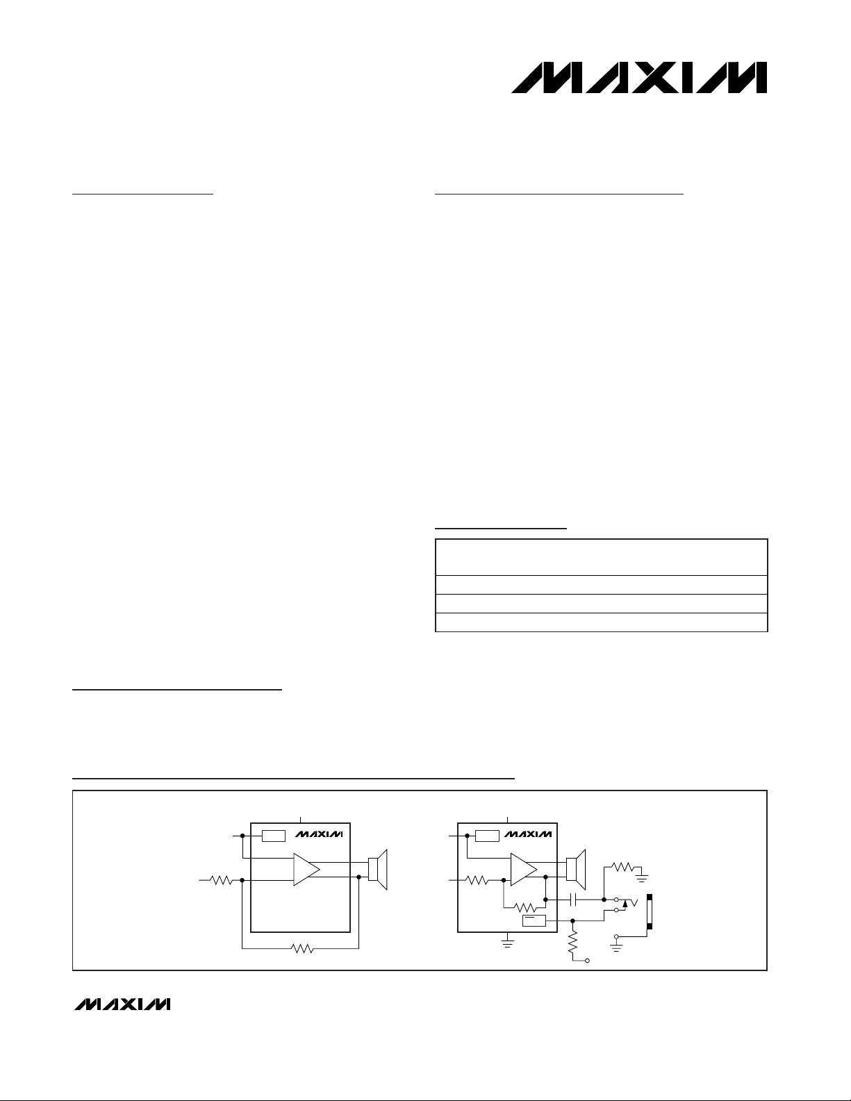
Simplified Block Diagrams
19-3146; Rev 0; 1/04
For pricing, delivery, and ordering information, please contact Maxim/Dallas Direct! at
1-888-629-4642, or visit Maxim’s website at www.maxim-ic.com.
Pin Configurations and Selector Guide appear at end of data
sheet.
UCSP is a trademark of Maxim Integrated Products, Inc.
*Future product—contact factory for availability.
**EP = Exposed paddle.
PART
TEMP RANGE
PINPACKAGE
GAIN
(dB)
MAX9716ETA
Adj.
MAX9716EBL-T*
3 x 3 UCSP
Adj.
MAX9716EUA
Adj.
Ordering Information continued at end of data sheet.
-40°C to +85°C 8 TDFN-EP**
-40°C to +85°C
-40°C to +85°C 8 µMAX-EP**
Page 2
MAX9716/MAX9717
Low-Cost, Mono, 1.4W BTL Audio Power
Amplifiers
2 _______________________________________________________________________________________
ABSOLUTE MAXIMUM RATINGS
ELECTRICAL CHARACTERISTICS—5V Supply
(VCC= 5V, GND = 0, SHDN = VCC, TA= +25°C. C
BIAS
= 1µF, RIN= RF= 20kΩ (MAX9716/MAX9717A), IN+ = BIAS (MAX9716),
BTL/SE = GND (MAX9717_), R
L
= ∞ connected between OUT+ and OUT-. Typical values are at TA= +25°C.) (Note 2)
Stresses beyond those listed under “Absolute Maximum Ratings” may cause permanent damage to the device. These are stress ratings only, and functional
operation of the device at these or any other conditions beyond those indicated in the operational sections of the specifications is not implied. Exposure to
absolute maximum rating conditions for extended periods may affect device reliability.
Supply Voltage (VCCto GND)..................................-0.3V to +6V
Any Other Pin to GND ...............................-0.3V to (V
CC
+ 0.3V)
IN_, BIAS, SHDN, BTL/SE Continuous Current...................20mA
OUT_ Short-Circuit Duration to GND or V
CC
(Note 1)...Continuous
Continuous Power Dissipation (T
A
= +70°C)
8-Pin TDFN (derate 24.4mW/°C above +70°C) .........1951mW
8-Pin µMAX (derate 10.3mW/°C above +70°C)...........825mW
9-Bump UCSP (derate 5.2mW/°C above 70°C)...........412mW
Operating Temperature Range ..........................-40°C to +85°C
Maximum Junction Temperature ....................................+150°C
Storage Temperature Range.............................-65°C to +150°C
Lead Temperature (soldering, 10s).................................+300°C
Bump Temperature (soldering)........................................+235°C
PARAMETER
SYMBOL
CONDITIONS
MIN
TYP
MAX
UNITS
Supply Voltage V
CC
Inferred by PSRR test 2.7 5.5 V
Quiescent Supply Current I
CC
V
IN-
= V
IN+
= V
BIAS
(Note 3),
T
A
= -40°C to +85°C
4.3 8 mA
Shutdown Supply Current I
SHDN
SHDN = GND
1µA
V
IH
1.2
SHDN Threshold
V
IL
0.4
V
V
IH
0.9 x
BTL/SE Threshold
V
IL
0.7 x
V
Common-Mode Bias Voltage V
BIAS
(Note 4)
V
CC
/2
VCC/2
V
Output Offset Voltage V
OS
V
IN-
= V
OUT+
, V
IN+
= V
BIAS
(Note 5) ±7
mV
VCC = 2.7V to 5.5V DC, V
BIAS
= 1.5V 60 80
f = 217Hz 61
Power-Supply Rejection Ratio PSRR
V
IN+
= V
BIAS
,
RL = 8Ω (Note 6)
f = 1kHz 73
dB
0.8 1.1
1.4
Output Power P
OUT
RL = 16Ω, BTL/SE = VCC (single-ended
mode), THD+N = 1%, f
IN
= 1kHz
W
Total Harmonic Distortion Plus
Noise
AV = 6dB, RL = 8Ω, fIN = 1kHz,
P
OUT
= 0.5W (Note 8)
%
Output Noise Density e
n
fIN = 10kHz
nV/√Hz
Signal-to-Noise Ratio SNR THD+N = 1%
dB
0.01
THD+N
V
RIPPLE
= 200mV
RL = 8Ω, THD+N = 1%, f
RL = 4Ω, THD+N = 1%, f
,
P-P
IN
IN
= 1kHz (Note 7)
= 1kHz (Note 7)
V
CC
V
/2
- 6%
CC
0.155
0.024
106
105
V
CC
+ 6%
±15
Page 3
MAX9716/MAX9717
Low-Cost, Mono, 1.4W BTL Audio Power
Amplifiers
_______________________________________________________________________________________ 3
ELECTRICAL CHARACTERISTICS—5V Supply (continued)
(VCC= 5V, GND = 0, SHDN = VCC, TA= +25°C. C
BIAS
= 1µF, RIN= RF= 20kΩ (MAX9716/MAX9717A), IN+ = BIAS (MAX9716),
BTL/SE = GND (MAX9717_), R
L
= ∞ connected between OUT+ and OUT-. Typical values are at TA= +25°C.) (Note 2)
PARAMETER
SYMBOL
CONDITIONS
MIN
TYP
MAX
UNITS
Output Short-Circuit Current Limit
I
SC
(Note 9) 1.1 A
Thermal Shutdown Threshold
°C
Thermal Shutdown Hysteresis 15 °C
Power-Up/Enable from Shutdown
Time (Note 10)
t
PU
C
BIAS
= 0.1µF 25
ms
Shutdown Time t
SHDN
5µs
Input Resistance R
IN
MAX9717B/C/D 12 20 28 kΩ
ELECTRICAL CHARACTERISTICS—3V Supply
(VCC= 3V, GND = 0, SHDN = VCC, TA= +25°C. C
BIAS
= 1µF, RIN= RF= 20kΩ (MAX9716/MAX9717A), IN+ = BIAS (MAX9716),
BTL/SE = GND (MAX9717_), R
L
= ∞ connected between OUT+ and OUT-. Typical values are at TA= +25°C.) (Note 2)
PARAMETER
SYMBOL
CONDITIONS
MIN
TYP
MAX
UNITS
Quiescent Supply Current I
CC
V
IN-
= V
IN+
= V
BIAS
(Note 3),
T
A
= -40°C to +85°C
4 8.0 mA
Shutdown Supply Current I
SHDN
SHDN = GND
1µA
V
IH
1.2
SHDN Threshold
V
IL
0.4
V
V
IH
0.9 x
BTL/SE Threshold
V
IL
0.7 x
V
Common-Mode Bias Voltage V
BIAS
(Note 4)
VCC/2
V
Output Offset Voltage V
OS
V
IN-
= V
OUT+
, V
IN+
= V
BIAS
(Note 5) ±7
mV
f = 217Hz 61
Power-Supply Rejection Ratio PSRR
V
IN+
= V
BIAS
,
RL = 8Ω (Note 6)
f = 1kHz 73
dB
Output Power P
OUT
mW
Total Harmonic Distortion Plus
Noise
AV = 6dB, RL = 8Ω, fIN = 1kHz,
P
OUT
= 0.5W, VCC = 3V (Note 8)
%
Output-Noise Density e
n
fIN = 10kHz
nV/√Hz
Signal-to-Noise Ratio SNR THD+N = 1%
dB
+160
250
0.01
V
V
RIPPLE
= 200mV
RL = 8Ω, THD+N = 1%, f
RL = 4Ω, THD+N = 1%, f
P-P
,
= 1kHz (Note 7) 350
IN
= 1kHz (Note 7) 525
IN
THD+N
CC
VCC/2
- 9%
/2
V
CC
0.024
106
100
V
CC
+ 9%
±15
Page 4
MAX9716/MAX9717
Low-Cost, Mono, 1.4W BTL Audio Power
Amplifiers
4 _______________________________________________________________________________________
ELECTRICAL CHARACTERISTICS—3V Supply (continued)
(VCC= 3V, GND = 0, SHDN = VCC, TA= +25°C. C
BIAS
= 1µF, RIN= RF= 20kΩ (MAX9716/MAX9717A), IN+ = BIAS (MAX9716),
BTL/SE = GND (MAX9717_), R
L
= ∞ connected between OUT+ and OUT-. Typical values are at TA= +25°C.) (Note 2)
PARAMETER
SYMBOL
CONDITIONS
MIN
TYP
MAX
UNITS
Output Short-Circuit Current Limit
I
SC
(Note 9) 1.1 A
Thermal Shutdown Threshold
°C
Thermal Shutdown Hysteresis 15 °C
Power-Up/Enable from Shutdown
Time (Note 10)
t
PU
C
BIAS
= 0.1µF 25
ms
Shutdown Time t
SHDN
5µs
Input Resistance R
IN
MAX9717B/C/D 12 20 28 kΩ
Note 1: Continuous power dissipation must also be observed.
Note 2: All specifications are tested at T
A
= +25°C. Specifications over temperature (TA = T
MIN
to T
MAX
) are not production tested,
and guaranteed by design.
Note 3: Quiescent power-supply current is specified and tested with no load. Quiescent power-supply current depends on the off-
set voltage when a practical load is connected to the amplifier.
Note 4: Common-mode bias voltage is the voltage on BIAS and is nominally V
CC
/2.
Note 5: V
OS
= V
OUT+
- V
OUT-.
Note 6: The amplifier input IN- is AC-coupled to GND through CIN.
Note 7: Output power is specified by a combination of a functional output current test and characterization analysis.
Note 8: Measurement bandwidth for THD+N is 22Hz to 22kHz.
Note 9: Extended short-circuit conditions result in a pulsed output.
Note 10: Time for V
OUT
to rise to 50% of final DC value.
+160
250
Page 5
MAX9716/MAX9717
Low-Cost, Mono, 1.4W BTL Audio Power
Amplifiers
_______________________________________________________________________________________ 5
TOTAL HARMONIC DISTORTION
PLUS NOISE vs. FREQUENCY
MAX9716 toc01
FREQUENCY (Hz)
THD+N (%)
10k1k100
0.01
0.1
1
10
100
0.001
10 100k
VCC = 5V
R
L
= 8
Ω
A
V
= 6dB
OUTPUT POWER = 800mW
OUTPUT POWER = 30mW
TOTAL HARMONIC DISTORTION
PLUS NOISE vs. FREQUENCY
MAX9716 toc02
FREQUENCY (Hz)
THD+N (%)
10k1k100
0.01
0.1
1
10
100
0.001
10 100k
VCC = 5V
R
L
= 8
Ω
A
V
= 12dB
OUTPUT POWER = 800mW
OUTPUT POWER = 200mW
TOTAL HARMONIC DISTORTION
PLUS NOISE vs. FREQUENCY
MAX9716 toc03
FREQUENCY (Hz)
THD+N (%)
10k1k100
0.01
0.1
1
10
100
0.001
10 100k
VCC = 3V
R
L
= 8
Ω
A
V
= 6dB
OUTPUT POWER = 250mW
OUTPUT POWER = 30mW
TOTAL HARMONIC DISTORTION
PLUS NOISE vs. FREQUENCY
MAX9716 toc04
FREQUENCY (Hz)
THD+N (%)
10k1k100
0.01
0.1
1
10
100
0.001
10 100k
VCC = 3V
R
L
= 8
Ω
A
V
= 12dB
OUTPUT POWER = 200mW
OUTPUT POWER = 50mW
TOTAL HARMONIC DISTORTION
PLUS NOISE vs. FREQUENCY
MAX9716 toc05
FREQUENCY (Hz)
THD+N (%)
10k1k100
0.01
0.1
1
10
100
0.001
10 100k
VCC = 5V
R
L
= 4
Ω
A
V
= 6dB
OUTPUT POWER = 1W
OUTPUT POWER = 200mW
TOTAL HARMONIC DISTORTION
PLUS NOISE vs. FREQUENCY
MAX9716 toc06
FREQUENCY (Hz)
THD+N (%)
10k1k100
0.01
0.1
1
10
100
0.001
10 100k
VCC = 5V
R
L
= 4
Ω
A
V
= 12dB
OUTPUT POWER = 250mW
OUTPUT POWER = 1W
TOTAL HARMONIC DISTORTION
PLUS NOISE vs. FREQUENCY
MAX9716 toc07
FREQUENCY (Hz)
THD+N (%)
10k1k100
0.01
0.1
1
10
100
0.001
10 100k
VCC = 3V
R
L
= 4
Ω
A
V
= 6dB
OUTPUT POWER = 50mW
OUTPUT POWER = 350mW
TOTAL HARMONIC DISTORTION
PLUS NOISE vs. FREQUENCY
MAX9716 toc08
FREQUENCY (Hz)
THD+N (%)
10k1k100
0.01
0.1
1
10
100
0.001
10 100k
VCC = 3V
R
L
= 4
Ω
A
V
= 12dB
OUTPUT POWER = 50mW
OUTPUT POWER = 350mW
TOTAL HARMONIC DISTORTION PLUS
NOISE vs. FREQUENCY (SINGLE-ENDED)
MAX9716 toc09
FREQUENCY (Hz)
THD+N (%)
10k1k100
0.001
0.01
0.1
1
10
100
0.0001
10 100k
VCC = 5V
R
L
= 16Ω
A
V
= 12dB
OUTPUT POWER = 125mW
OUTPUT POWER = 25mW
Typical Operating Characteristics
(VCC= 5V, THD+N measurement bandwidth = 22Hz to 22kHz, BTL mode, TA= +25°C, unless otherwise noted.)
Page 6
MAX9716/MAX9717
Low-Cost, Mono, 1.4W BTL Audio Power
Amplifiers
6 _______________________________________________________________________________________
Typical Operating Characteristics (continued)
(VCC= 5V, THD+N measurement bandwidth = 22Hz to 22kHz, BTL mode, TA= +25°C, unless otherwise noted.)
TOTAL HARMONIC DISTORTION PLUS
NOISE vs. OUTPUT POWER
MAX9716 toc10
OUTPUT POWER (W)
THD+N (%)
1.21.00.80.60.40.2
0.01
0.1
1
10
100
0.001
01.4
VCC = 5V
R
L
= 8Ω
A
V
= 6dB
fIN = 100Hz
fIN = 1kHz
fIN = 10kHz
TOTAL HARMONIC DISTORTION PLUS
NOISE vs. OUTPUT POWER
MAX9716 toc11
OUTPUT POWER (W)
THD+N (%)
1.41.21.00.80.60.40.2
0.01
0.1
1
10
100
0.001
0
VCC = 5V
R
L
= 8Ω
A
V
= 12dB
fIN = 1kHz
fIN = 100Hz
fIN = 10kHz
TOTAL HARMONIC DISTORTION PLUS
NOISE vs. OUTPUT POWER
MAX9716 toc12
OUTPUT POWER (mW)
THD+N (%)
400300200100
0.01
0.1
1
10
100
0.001
0 500
VCC = 3V
R
L
= 8Ω
A
V
= 6dB
fIN = 100Hz
fIN = 1kHz
fIN = 10kHz
TOTAL HARMONIC DISTORTION PLUS
NOISE vs. OUTPUT POWER
MAX9716 toc13
OUTPUT POWER (mW)
THD+N (%)
400300200100
0.01
0.1
1
10
100
0.001
0 500
VCC = 3V
R
L
= 8Ω
A
V
= 12dB
fIN = 100Hz
fIN = 1kHz
fIN = 10kHz
TOTAL HARMONIC DISTORTION PLUS
NOISE vs. OUTPUT POWER
MAX9716 toc14
OUTPUT POWER (W)
THD+N (%)
1.81.61.41.21.00.80.60.40.2
0.01
0.1
1
10
100
0.001
0 2.0
VCC = 5V
R
L
= 4Ω
A
V
= 6dB
fIN = 1kHz
fIN = 100Hz
fIN = 10kHz
TOTAL HARMONIC DISTORTION PLUS
NOISE vs. OUTPUT POWER
MAX9716 toc15
OUTPUT POWER (W)
THD+N (%)
1.81.61.41.21.00.80.60.40.2
0.01
0.1
1
10
100
0.001
02.0
fIN = 100Hz
fIN = 1kHz
VCC = 5V
R
L
= 4Ω
A
V
= 12dB
fIN = 10kHz
TOTAL HARMONIC DISTORTION PLUS
NOISE vs. OUTPUT POWER
MAX9716 toc16
OUTPUT POWER (mW)
THD+N (%)
700600500400300200100
0.01
0.1
1
10
100
0.001
0 800
fIN = 10kHz
fIN = 100Hz
fIN = 1kHz
VCC = 3V
R
L
= 4Ω
A
V
= 6dB
TOTAL HARMONIC DISTORTION PLUS
NOISE vs. OUTPUT POWER
MAX9716 toc17
OUTPUT POWER (mW)
THD+N (%)
700600500400300200100
0.01
0.1
1
10
100
0.001
0 800
VCC = 3V
R
L
= 4Ω
A
V
= 12dB
fIN = 1kHz
fIN = 100Hz
fIN = 10kHz
TOTAL HARMONIC DISTORTION PLUS NOISE
vs. OUTPUT POWER (SINGLE-ENDED)
MAX9716 toc18
OUTPUT POWER (mW)
THD+N (%)
225200175150125100755025
0.01
0.1
1
10
100
0.001
0 250
VCC = 5V
R
L
= 16Ω
A
V
= 6dB
fIN = 100Hz
fIN = 10kHz
fIN = 1kHz
Page 7
MAX9716/MAX9717
Low-Cost, Mono, 1.4W BTL Audio Power
Amplifiers
_______________________________________________________________________________________ 7
OUTPUT POWER
vs. SUPPLY VOLTAGE
MAX9716 toc19
SUPPLY VOLTAGE (V)
OUTPUT POWER (W)
5.04.54.03.53.0
0.3
0.6
0.9
1.2
1.5
1.8
0
2.5 5.5
RL = 8Ω
f = 1kHz
A
V
= 6dB
THD+N = 10%
THD+N = 1%
1.5
2.0
2.5
3.0
0
OUTPUT POWER
vs. SUPPLY VOLTAGE
MAX9716 toc20
SUPPLY VOLTAGE (V)
OUTPUT POWER (W)
5.04.54.03.53.02.5 5.5
THD+N = 10%
THD+N = 1%
RL = 4Ω
f = 1kHz
A
V
= 6dB
1.0
0.5
OUTPUT POWER
vs. LOAD RESISTANCE
MAX9716 toc21
LOAD RESISTANCE (Ω)
OUTPUT POWER (mW)
10
0.5
1.0
1.5
2.0
2.5
0
1 100
THD+N = 1%
THD+N = 10%
VCC = 5V
f = 1kHz
A
V
= 6dB
100
200
300
400
500
600
700
0
OUTPUT POWER
vs. LOAD RESISTANCE
MAX9716 toc22
LOAD RESISTANCE (Ω)
OUTPUT POWER (mW)
101 100
VCC = 3V
f = 1kHz
A
V
= 6dB
THD+N = 1%
THD+N = 10%
POWER DISSIPATION
vs. OUTPUT POWER
MAX9716 toc23
OUTPUT POWER (W)
POWER DISSIPATION (W)
1.20.90.60.3
0.2
0.4
0.6
0.8
1.0
0
01.5
VCC = 5V
R
L
= 8Ω
f = 1kHz
A
V
= 6dB
50
100
150
200
250
300
0
POWER DISSIPATION
vs. OUTPUT POWER
MAX9716 toc24
OUTPUT POWER (mW)
POWER DISSIPATION (mW)
4003002001000 500
VCC = 3V
R
L
= 8Ω
f = 1kHz
A
V
= 6dB
POWER DISSIPATION
vs. OUTPUT POWER
MAX9716 toc25
OUTPUT POWER (W)
POWER DISSIPATION (W)
1.61.20.80.4
0.4
0.8
1.2
1.6
2.0
0
02.0
VCC = 5V
R
L
= 4Ω
f = 1kHz
A
V
= 6dB
600500400300200100
100
200
300
400
500
600
700
0
0700
POWER DISSIPATION
vs. OUTPUT POWER
MAX9716 toc26
OUTPUT POWER (mW)
POWER DISSIPATION (mW)
VCC = 3V
R
L
= 4Ω
f = 1kHz
A
V
= 6dB
OUTPUT-NOISE DENSITY
vs. FREQUENCY
MAX9716 toc27
FREQUENCY (Hz)
OUTPUT-NOISE DENSITY (nV/
√
Hz)
10k1k
100
200
300
400
500
600
0
100 100k
AV = 6dB
Typical Operating Characteristics (continued)
(VCC= 5V, THD+N measurement bandwidth = 22Hz to 22kHz, BTL mode, TA= +25°C, unless otherwise noted.)
Page 8
MAX9716/MAX9717
Low-Cost, Mono, 1.4W BTL Audio Power
Amplifiers
8 _______________________________________________________________________________________
Typical Operating Characteristics (continued)
(VCC= 5V, THD+N measurement bandwidth = 22Hz to 22kHz, BTL mode, TA= +25°C, unless otherwise noted.)
GAIN AND PHASE vs. FREQUENCY
MAX9716 toc28
FREQUENCY (Hz)
GAIN AND PHASE (°/dB)
1M100k100 1k 10k
-90
-60
-30
0
30
60
90
120
-120
10 10M
AV = 60dB
POWER-SUPPLY REJECTION RATIO
vs. FREQUENCY
MAX9716 toc29
FREQUENCY (Hz)
PSRR (dB)
10k1k100
-90
-80
-70
-60
-50
-40
-30
-20
-10
0
10 100k
SUPPLY CURRENT vs. V
CC
MAX9716 toc30
VCC (V)
SUPPLY CURRENT (mA)
5.14.73.1 3.5 3.9 4.3
2.5
3.0
3.5
4.0
4.5
5.0
5.5
6.0
2.0
2.7 5.5
SUPPLY CURRENT
vs. TEMPERATURE
MAX9716 toc31
TEMPERATURE (°C)
SUPPLY CURRENT (mA)
603510-15
1
2
3
4
5
6
-40 85
VCC = 3V
VCC = 5V
COMING OUT OF SHUTDOWN
MAX9716 toc32
OUT+
1V/div
OUT+ - OUT200mV/div
OUT1V/div
SHDN
2V/div
100ms/div
RL = 8
Ω
GOING INTO SHUTDOWN
MAX9716 toc33
OUT+
1V/div
OUT+ - OUT200mV/div
OUT1V/div
SHDN
2V/div
10µs/div
RL = 8
Ω
SHUTDOWN CURRENT vs. V
CC
MAX9716 toc34
VCC (V)
SHUTDOWN CURRENT (nA)
5.04.54.03.53.0
2
4
6
8
10
12
14
16
18
20
0
2.5 5.5
SHUTDOWN CURRENT
vs. TEMPERATURE
MAX9716 toc35
TEMPERATURE (°C)
SHUTDOWN CURRENT (nA)
6035-15 10
5
10
15
20
25
30
35
40
0
-40 85
VCC = 5V
VCC = 3V
Page 9

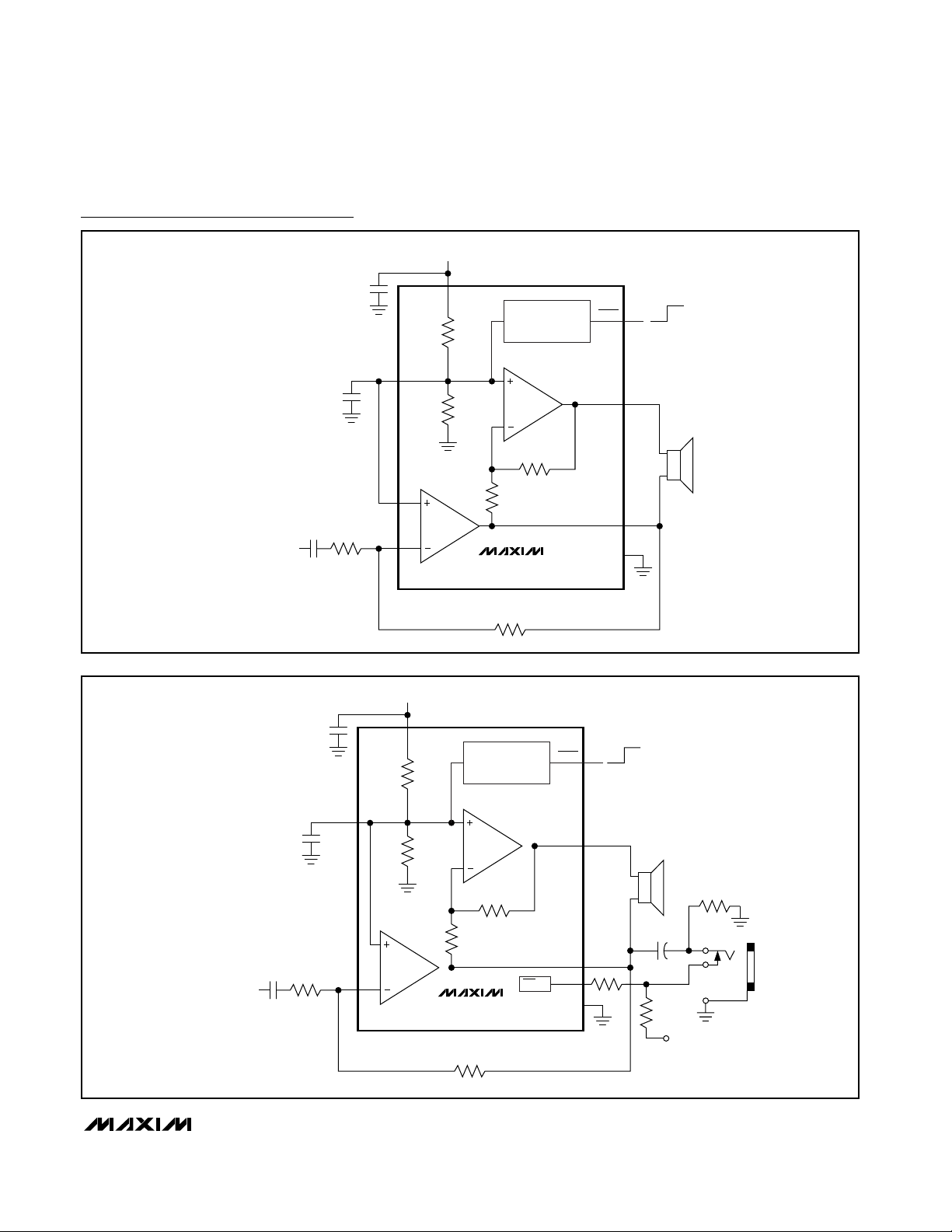
Detailed Description
The MAX9716/MAX9717 are 1.3W BTL speaker amplifiers. Both devices feature a low-power shutdown
mode, and industry-leading click-and-pop suppression.
The MAX9717 features a headphone sense input that
disables the slave BTL amplifier to drive the headphone
as a single-ended load. These devices consist of high
output-current audio amps configured as BTL amplifiers (see Functional Diagrams). The closed-loop gain
of the input op amp sets the single-ended gain of the
device. Two external gain resistors set the gain of the
MAX9716 and MAX9717A (see the Gain-Setting
Resistor section). The MAX9717B/C/D feature internally
set gains of 6dB, 9dB, and 12dB, respectively.
The output of the first amplifier serves as the input of the
second amplifier, which is configured as an inverting
unity-gain follower. This results in two outputs, identical in
amplitude, but 180° out-of-phase.
BIAS
The MAX9716/MAX9717 operate from a single 2.7V to
5.5V supply and feature an internally generated, commonmode bias voltage of VCC/2 referenced to ground. BIAS
provides both click-and-pop suppression and sets the DC
bias level for the audio outputs. The MAX9716 can be
configured as a single-ended or differential input. For single-ended input, connect the noninverting input IN+ to
BIAS externally. The MAX9717 BIAS is internally connected to the amplifier noninverting input IN+.
The MAX9717 can only be used with a single-ended
input. Always bypass BIAS to ground with a capacitor.
Choose the value of the bypass capacitor as described in
the BIAS Capacitor section. Do not connect external loads
to BIAS. Any load lowers the BIAS voltage, affecting the
overall performance of the device.
BTL
/SE Control Input
The MAX9717 features a headphone sense input,
BTL/SE, that enables headphone jack sensing to control the power amplifier output configuration. Driving
BTL/SE low enables the slave amplifier (OUT-). Driving
BTL/SE high disables the slave amplifier.
Shutdown Mode
The MAX9716/MAX9717 feature a low-power shutdown
mode that reduces quiescent current consumption to
10nA. Entering shutdown disables the bias circuitry,
forces the amplifier outputs to GND through an internal
20kΩ resistor. Drive SHDN low to enter shutdown
mode; drive SHDN high for normal operation.
Click-and-Pop Suppression
The MAX9716/MAX9717 feature Maxim’s industry-leading
click-and-pop suppression circuitry. During startup, the
amplifier common-mode bias voltage ramps to the DC
bias. When entering shutdown, the amplifier outputs are
pulled to GND through an internal 20kΩ resistor. This
scheme minimizes the energy present in the audio band.
MAX9716/MAX9717
Low-Cost, Mono, 1.4W BTL Audio Power
Amplifiers
_______________________________________________________________________________________ 9
Pin Description
PIN BUMP
TDFN/µMAX UCSP
MAX9716
FUNCTION
1 1 C3 C3 SHDN Active-Low Shutdown
2 2 C1 C1 BIAS
DC Bias Bypass Capacitor Connection. Bypass BIAS to ground with a
1µF capacitor.
3 — A3 — IN+ Noninverting Input
4 4 A1 A1 IN- Inverting Input
5 5 A2 A2 OUT+ Bridge Amplifier Positive Output
6 6 B3 B3 V
CC
Power Supply. Bypass VCC with a 1µF capacitor to ground.
77
GND Ground
8 8 C2 C2 OUT-
Bridge Amplifier Negative Output. OUT- becomes high-impedance
when BTL/SE is driven high.
—3—A3
BTL/Single-Ended Mode Input. Logic low sets the device in BTL mode.
Logic high sets the device in single-ended mode.
EP EP — — EP Exposed Pad. Connect EP to GND.
NAME
MAX9717 MAX9716 MAX9717
B1, B2 B1, B2
BTL/SE
Page 10

MAX9716/MAX9717
Applications Information
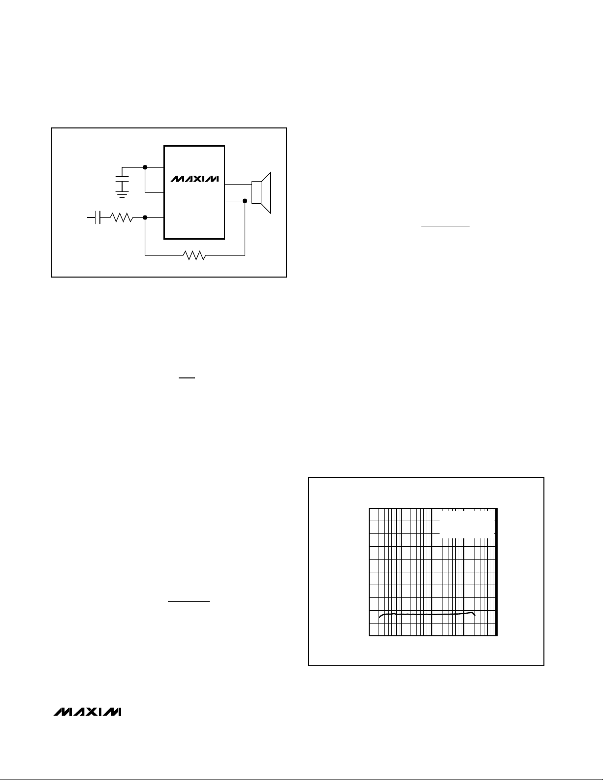
BTL Amplifier
The MAX9716/MAX9717 are designed to drive a load
differentially, a configuration referred to as bridge-tied
load or BTL. The BTL configuration (Figure 1) offers
advantages over the single-ended configuration, where
one side of the load is connected to ground. Driving the
load differentially doubles the output voltage compared
to a single-ended amplifier under similar conditions.
Thus, the differential gain of the device is twice the
closed-loop gain of the input amplifier. The effective
gain is given by:
Substituting 2 x V
OUT(P-P)
for V
OUT(P-P)
into the following
equations yields four times the output power due to
doubling of the output voltage:
There is no net DC voltage across the load because the
differential outputs are each biased at midsupply. This
eliminates the need for DC-blocking capacitors
required for single-ended amplifiers. These capacitors
can be large and expensive, consume board space,
and degrade low-frequency performance.
Power Dissipation and Heat Sinking
Under normal operating conditions, the MAX9716/
MAX9717 dissipate a significant amount of power. The
maximum power dissipation for each package is given
in the Absolute Maximum Ratings section under
Continuous Power Dissipation or can be calculated by
the following equation:
where T
J(MAX)
is +150°C, TAis the ambient temperature,
and θJAis the reciprocal of the derating factor in °C/W as
specified in the Absolute Maximum Ratings section. For
example, θJAof the TDFN package is 41°C/W.
The increase in power delivered by the BTL configuration
directly results in an increase in internal power dissipation
over the single-ended configuration. The maximum power
dissipation for a given VCCand load is given by the
following equation:
If the power dissipation for a given application exceeds
the maximum allowed for a given package, reduce
power dissipation by increasing the ground plane heatsinking capability and the size of the traces to the device
(see the Layout and Grounding section). Other methods
for reducing power dissipation are to reduce VCC,
increase load impedance, decrease ambient temperature, reduce gain, or reduce input signal.
Thermal-overload protection limits total power dissipation
in the MAX9716/MAX9717. Thermal protection circuitry
disables the amplifier output stage when the junction
temperature exceeds +160°C. The amplifiers are
enabled once the junction temperature cools by 15°C. A
pulsing output under continuous thermal-overload conditions results as the device heats and cools.
Fixed Gain
The MAX9717B, MAX9717C, and MAX9717D feature
internally fixed gains of 6dB, 9dB, and 12dB, respectively (see the Selector Guide). Fixed gain simplifies
designs, reduces pin count, decreases required footprint size, and eliminates external gain-setting resistors.
Resistors RINand RFshown in the MAX9717B/C/D
Typical Operating Circuit are used to achieve each
fixed gain.
P
V
R
DISS MAX
CC
L
()
=
2
2
2
π
P
TT
DISSPKG MAX
J MAX A
JA
()
()
=
−
θ
P
V
R
OUT
RMS
L
=
2
V
V
RMS
OUT P P
()
=
−
22
A
R
R
V
F
IN
=×2
Low-Cost, Mono, 1.4W BTL Audio Power
Amplifiers
10 ______________________________________________________________________________________
+1
V
OUT(P-P)
2 x V
OUT(P-P)
V
OUT(P-P)
-1
Figure 1. Bridge-Tied Load Configuration
Page 11
Adjustable Gain
Gain-Setting Resistors
External feedback resistors set the gain of the
MAX9716 and MAX9717A. Resistors RFand RIN(see
Figure 2) set the gain of the amplifier as follows:
Where AVis the desired voltage gain. Hence, an RINof
20kΩ and an RFof 20kΩ yields a gain of 2V/V, or 6dB.
RFcan be either fixed or variable, allowing the use of a
digitally controlled potentiometer to alter the gain under
software control.
The gain of the MAX9717 in a single-ended output
configuration is half the gain when configured as BTL
output. Choose RFbetween 10kΩ and 50kΩ for the
MAX9716 and MAX9717A. Gains for the MAX9717B/C/D
are set internally.
Input Filter
C
IN
and RINform a highpass filter that removes the DC
bias from an incoming signal. The AC-coupling capacitor allows the amplifier to bias the signal to an optimal
DC level. Assuming zero-source impedance, the -3dB
point of the highpass filter is:
Setting f
-3dB
too high affects the low-frequency
response of the amplifier. Use capacitors with
dielectrics that have low-voltage coefficients, such as
tantalum or aluminum electrolytic. Capacitors with highvoltage coefficients, such as ceramics, can increase
distortion at low frequencies.
Output-Coupling Capacitor
The MAX9717 require output-coupling capacitors to
operate in single-ended (headphone) mode. The output-coupling capacitor blocks the DC component of the
amplifier output, preventing DC current from flowing to
the load. The output capacitor and the load impedance
form a highpass filter with a -3dB point determined by:
As with the input capacitor, choose C
OUT
such that
f
-3dB
is well below the lowest frequency of interest.
Setting f
-3dB
too high affects the amplifier’s low-frequency response. Load impedance is a concern when
choosing C
OUT
. Load impedance can vary, changing
the -3dB point of the output filter. A lower impedance
increases the corner frequency, degrading low-frequency response. Select C
OUT
such that the worst-
case load/C
OUT
combination yields an adequate
response. Select capacitors with low ESR to minimize
resistive losses and optimize power transfer to the load.
Differential Input
The MAX9716 can be configured for a differential input.
The advantage of differential inputs is that any common-mode noise is attenuated and not passed through
the amplifier. This input improves noise rejection and
provides common-mode rejection (Figure 3). External
components should be closely matched for high
CMRR. Figure 4 shows the MAX9716 configured for a
differential input.
f
RC
dB
L OUT
−=3
1
2
π
f
RC
dB
IN IN
−=3
1
2
π
A
R
R
V
F
IN
=
⎛
⎝
⎜
⎞
⎠
⎟
2
MAX9716/MAX9717
Low-Cost, Mono, 1.4W BTL Audio Power
Amplifiers
______________________________________________________________________________________ 11
OUTOUT+
MAX9716
R
F
IN-
IN+
BIAS
R
IN
C
IN
AUDIO
INPUT
Figure 2. Setting the MAX9716/MAX9717A Gain
FREQUENCY (Hz)
CMRR (dB)
10k1k100
-90
-80
-70
-60
-50
-40
-30
-20
-10
0
-100
10 100k
V
RIPPLE
= 200mV
P-P
RL = 8Ω
C
BIAS
= 1µF
COMMON-MODE REJECTION RATIO
vs. FREQUENCY
Figure 3. CMRR with Differential Input
Page 12

MAX9716/MAX9717
BIAS Capacitor
BIAS is the output of the internally-generated VCC/2 bias
voltage. The BIAS bypass capacitor, C
BIAS
, improves the
power-supply rejection ratio by reducing power supply
and other noise sources at the common-mode bias node.
C
BIAS
also generates the clickless/popless startup DC
bias waveform for the speaker amplifiers. Bypass BIAS
with a 1µF capacitor to GND. Larger C
BIAS
values
improve PSRR but slow down tONtime. Do not connect
external loads to BIAS.
Supply Bypassing
Proper power-supply bypassing ensures low-noise,
low-distortion performance. Connect a 1µF ceramic
capacitor from VCCto GND. Add additional bulk
capacitance as required by the application. Connect
the bypass capacitor as close to the device as possible.
Layout and Grounding
Proper PC board layout and grounding is essential for
optimizing performance. Use large traces for the
power-supply inputs and amplifier outputs to minimize
losses due to parasitic trace resistance. Large traces
also aid in moving heat away from the package. Proper
grounding improves audio performance and prevents
digital switching noise from coupling into the audio signal.
The MAX9716/MAX9717 TDFN and µMAX packages
feature exposed thermal pads on their undersides. This
pad lowers the thermal resistance of the package by
providing a direct-heat conduction path from the die to
the printed circuit board. Connect the exposed pad to
the ground plane using multiple vias, if required.
Low-Cost, Mono, 1.4W BTL Audio Power
Amplifiers
12 ______________________________________________________________________________________
CLICKLESS/POPLESS
SHUTDOWN
CONTROL
BIAS
IN+
IN-
OUT+
OUT-
SHDN
GND
MAX9716
R
F
20kΩ
R
F
20kΩ
V
CC
R
IN
20kΩ
C
IN
0.33µF
AUDIO
INPUT
R
IN
20kΩ
C
IN
0.33µF
AUDIO
INPUT
C
BIAS
220pF
220pF
20kΩ
20kΩ
V
CC
VALUES SHOWN FOR 0dB GAIN.
OFF
ON
Figure 4. MAX9716 Differential Input
Page 13

UCSP Applications Information
For the latest application details on UCSP construction,
dimensions, tape carrier information, printed circuit board
techniques, bump-pad layout, and recommended reflow
temperature profile, as well as the latest information on
reliability testing results, refer to the application note,
“UCSP—A Wafer-Level Chip-Scale Package” available
on Maxim’s web site at http://www.maxim-ic.com/ucsp.
UCSP Marking Information
Pin A1 Bump Indicator
AAA: Product ID code
XXX: Lot Code
Chip Information
TRANSISTOR COUNT: 4877
PROCESS: BiCMOS
MAX9716/MAX9717
Low-Cost, Mono, 1.4W BTL Audio Power
Amplifiers
______________________________________________________________________________________ 13
Selector Guide
PART BTL/SE INPUT GAIN (dB)
MAX9716 — Adjustable
MAX9717A √ Adjustable
MAX9717B √ 6
MAX9717C √ 9
MAX9717D √ 12
Ordering Information (continued)
PART
TEMP RANGE
PINPACKAGE
GAIN
(dB)
MAX9717AEBL-T*
3 x 3 UCSP
Adj.
MAX9717AETA
Adj.
MAX9717AEUA
Adj.
MAX9717BEBL-T*
3 x 3 UCSP 6
MAX9717BETA
6
MAX9717BEUA
6
MAX9717CEBL-T*
3 x 3 UCSP 9
MAX9717CETA
9
MAX9717CEUA
9
MAX9717DEBL-T*
3 x 3 UCSP 12
MAX9717DETA
12
MAX9717DEUA
12
*Future product—contact factory for availability.
**EP = Exposed paddle.
AAA
XXX
-40°C to +85°C
-40°C to +85°C 8 TDFN-EP**
-40°C to +85°C 8 µMAX-EP**
-40°C to +85°C
-40°C to +85°C 8 TDFN-EP**
-40°C to +85°C 8 µMAX-EP**
-40°C to +85°C
-40°C to +85°C 8 TDFN-EP**
-40°C to +85°C 8 µMAX-EP**
-40°C to +85°C
-40°C to +85°C 8 TDFN-EP**
-40°C to +85°C 8 µMAX-EP**
Page 14

MAX9716/MAX9717
Low-Cost, Mono, 1.4W BTL Audio Power
Amplifiers
14 ______________________________________________________________________________________
V
CC
OUT+IN-
1
2
87OUT-
GNDBIAS
BTL/SE
SHDN
µMAX
3
4
6
5
MAX9717
IN- OUT+ BTL/SE
BIAS SHDNOUT-
GND V
CC
GND
UCSP
(1.5mm x 1.5mm)
MAX9717
A
B
C
123
TDFN
(3mm x 3mm x 0.8mm)
MAX9716
1
2
3
4
8
7
6
5
SHDN
BIAS
IN+
IN-
OUT-
GND
V
CC
OUT+
TDFN
(3mm x 3mm x 0.8mm)
MAX9717
1
2
3
4
8
7
6
5
SHDN
BIAS
BTL/SE
IN-
OUT-
GND
V
CC
OUT+
TOP VIEW
V
CC
OUT+IN-
1
2
87OUT-
GNDBIAS
IN+
SHDN
µMAX
3
4
6
5
MAX9716
TOP VIEW
(BUMPS ON BOTTOM)
IN- OUT+ IN+
BIAS SHDNOUT-
GND V
CC
GND
UCSP
(1.5mm x 1.5mm)
MAX9716
A
B
C
123
Pin Configurations
Page 15
MAX9716/MAX9717
Low-Cost, Mono, 1.4W BTL Audio Power
Amplifiers
______________________________________________________________________________________ 15
CLICKLESS/POPLESS
SHUTDOWN
CONTROL
BIAS
IN+
IN-
OUT+
OUT-
SHDN
GND
MAX9716
R
F
40kΩ
V
CC
R
IN
20kΩ
C
IN
0.33µF
AUDIO
INPUT
C
BIAS
1µF
20kΩ
20kΩ
V
CC
VALUES SHOWN FOR 12dB GAIN.
1µF
OFF
ON
Functional Diagrams/Typical Operating Circuits
CLICKLESS/POPLESS
SHUTDOWN
CONTROL
BIAS
IN-
OUT+
OUT-
SHDN
GND
MAX9717A
R
F
40kΩ
V
CC
R
IN
20kΩ
C
IN
0.33µF
AUDIO
INPUT
C
BIAS
1µF
20kΩ
20kΩ
V
CC
VALUES SHOWN FOR BTL 12dB GAIN,
HEADPHONE 6dB GAIN.
1µF
BTL/SE
C
OUT
100µF
100kΩ
V
CC
1kΩ
OFF
ON
100kΩ
Page 16

MAX9716/MAX9717
Low-Cost, Mono, 1.4W BTL Audio Power
Amplifiers
16 ______________________________________________________________________________________
CLICKLESS/POPLESS
SHUTDOWN
CONTROL
BIAS
IN-
OUT+
OUT-
SHDN
GND
MAX9717B
MAX9717C
MAX9717D
R
F
V
CC
R
IN
20kΩ
C
IN
0.33µF
AUDIO
INPUT
C
BIAS
1µF
20kΩ
20kΩ
V
CC
1µF
BTL/SE
C
OUT
100µF
100kΩ
V
CC
1kΩ
IN+
OFF
ON
100kΩ
Functional Diagrams/Typical Operating Circuits (continued)
Page 17

MAX9716/MAX9717
Low-Cost, Mono, 1.4W BTL Audio Power
Amplifiers
______________________________________________________________________________________ 17
Package Information
(The package drawing(s) in this data sheet may not reflect the most current specifications. For the latest package outline information,
go to www.maxim-ic.com/packages.)
8L, µMAX, EXP PAD.EPS
Page 18

MAX9716/MAX9717
Low-Cost, Mono, 1.4W BTL Audio Power
Amplifiers
18 ______________________________________________________________________________________
Package Information (continued)
(The package drawing(s) in this data sheet may not reflect the most current specifications. For the latest package outline information,
go to www.maxim-ic.com/packages.)
6, 8, &10L, DFN THIN.EPS
PROPRIETARY INFORMATION
TITLE:
APPROVAL
DOCUMENT CONTROL NO. REV.
2
1
PACKAGE OUTLINE, 6, 8 & 10L,
TDFN, EXPOSED PAD, 3x3x0.80 mm
21-0137 D
L
C
L
C
SEMICONDUCTOR
DALLAS
A2
A
PIN 1
INDEX
AREA
D
E
A1
D2
b
E2
[(N/2)-1] x e
REF.
e
k
1N1
L
e
L
A
L
PIN 1 ID
C0.35
DETAIL A
e
NUMBER OF LEADS SHOWN ARE FOR REFERENCE ONLY
DOCUMENT CONTROL NO.APPROVAL
TITLE:
PROPRIETARY INFORMATION
REV.
2
2
COMMON DIMENSIONS
SYMBOL
MIN. MAX.
A
0.70 0.80
D
2.90 3.10
E
2.90 3.10
A1
0.00 0.05
L
0.20 0.40
PKG. CODE
6
N
T633-1 1.50±0.10D22.30±0.10
E2
0.95 BSCeMO229 / WEEA
JEDEC SPEC
0.40±0.05b1.90 REF
[(N/2)-1] x e
1.50±0.10
MO229 / WEEC
1.95 REF0.30±0.05
0.65 BSC
2.30±0.10T833-1 8
PACKAGE VARIATIONS
21-0137
0.25±0.05 2.00 REFMO229 / WEED-30.50 BSC1.50±0.10 2.30±0.1010T1033-1
0.25 MIN.
k
A2 0.20 REF.
D
SEMICONDUCTOR
DALLAS
PACKAGE OUTLINE, 6, 8 & 10L,
TDFN, EXPOSED PAD, 3x3x0.80 mm
Page 19

MAX9716/MAX9717
Low-Cost, Mono, 1.4W BTL Audio Power
Amplifiers
Maxim cannot assume responsibility for use of any circuitry other than circuitry entirely embodied in a Maxim product. No circuit patent licenses are
implied. Maxim reserves the right to change the circuitry and specifications without notice at any time.
Maxim Integrated Products, 120 San Gabriel Drive, Sunnyvale, CA 94086 408-737-7600 ___________________ 19
© 2004 Maxim Integrated Products Printed USA is a registered trademark of Maxim Integrated Products.
Package Information (continued)
(The package drawing(s) in this data sheet may not reflect the most current specifications. For the latest package outline information,
go to www.maxim-ic.com/packages.)
 Loading...