

Page 1
General Description
The MAX9703/MAX9704 mono/stereo class D audio
power amplifiers provide class AB amplifier performance
with class D efficiency, conserving board space and
eliminating the need for a bulky heatsink. Using a class
D architecture, these devices deliver up to 15W while
offering up to 78% efficiency. Proprietary and patent-protected modulation and switching schemes render the traditional class D output filter unnecessary.
The MAX9703/MAX9704 offer two modulation schemes:
a fixed-frequency mode (FFM), and a spread-spectrum
mode (SSM) that reduces EMI-radiated emissions due
to the modulation frequency. The device utilizes a fully
differential architecture, a full bridged output, and comprehensive click-and-pop suppression.
The MAX9703/MAX9704 feature high 80dB PSRR, low
0.07% THD+N, and SNR in excess of 100dB. Short-circuit and thermal-overload protection prevent the
devices from being damaged during a fault condition.
The MAX9703 is available in a 32-pin TQFN (5mm x
5mm x 0.8mm) package. The MAX9704 is available in a
32-pin TQFN (7mm x 7mm x 0.8mm) package. Both
devices are specified over the extended -40°C to
+85°C temperature range.
Applications
Features
♦ Filterless Class D Amplifier
♦ Unique Spread-Spectrum Mode Offers 5dB
Emissions Improvement Over Conventional
Methods
♦ Up to 78% Efficient
♦ 15W Output Power into 8Ω
♦ Up to 20W Peak Power
♦ Low 0.07% THD+N
♦ High PSRR (80dB at 1kHz)
♦ 10V to 25V Single-Supply Operation
♦ Differential Inputs Minimize Common-Mode Noise
♦ Pin-Selectable Gain Reduces Component Count
♦ Industry-Leading Click-and-Pop Suppression
♦ Low Quiescent Current (24mA)
♦ Low-Power Shutdown Mode (0.2µA)
♦ Short-Circuit and Thermal-Overload Protection
♦ Available in Thermally Efficient, Space-Saving
Packages
32-Pin TQFN (5mm x 5mm x 0.8mm)–MAX9703
32-Pin TQFN (7mm x 7mm x 0.8mm)–MAX9704
MAX9703/MAX9704
15W, Filterless, Spread-Spectrum
Mono/Stereo Class D Amplifiers
________________________________________________________________ Maxim Integrated Products 1
19-3160; Rev 1; 3/04
For pricing, delivery, and ordering information, please contact Maxim/Dallas Direct! at
1-888-629-4642, or visit Maxim’s website at www.maxim-ic.com.
Ordering Information
PART
AMP
MAX9703ETJ
32 TQFN-EP*
Mono
MAX9704ETJ
32 TQFN-EP*
Stereo
*EP = Exposed paddle.
LCD TVs
LCD Monitors
Desktop PCs
LCD Projectors
Hands-Free Car
Phone Adaptors
Automotive
Pin Configurations appear at end of data sheet.
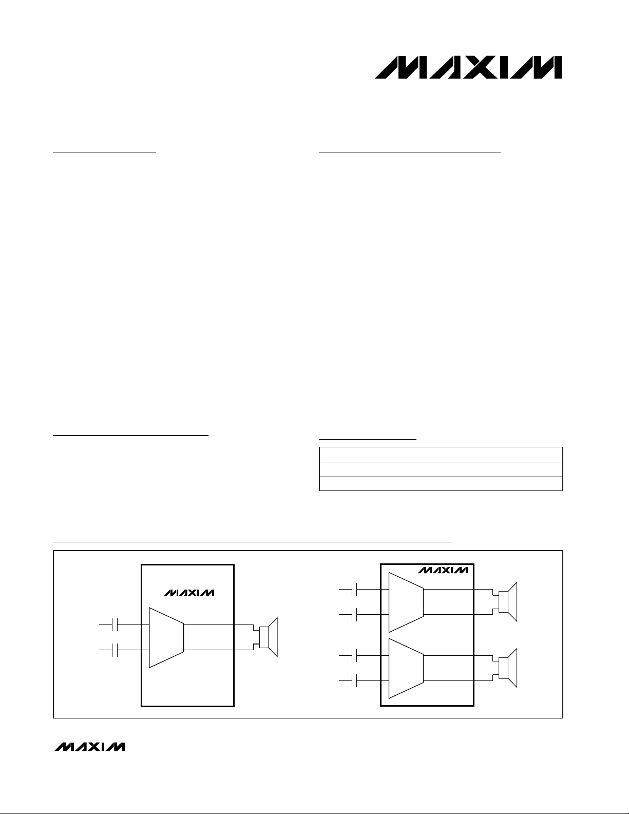
MAX9704
0.47µF
INL+ OUTL+
OUTL-INL-
0.47µF
H-BRIDGE
0.47µF
INR+ OUTR+
OUTR-INR-
0.47µF
H-BRIDGE
MAX9703
0.47µF
IN+ OUT+
OUT-
IN-
0.47µF
H-BRIDGE
Block Diagrams
TEMP RANGE
-40oC to +85oC
-40oC to +85oC
PIN-PACKAGE
Page 2
MAX9703/MAX9704
15W, Filterless, Spread-Spectrum
Mono/Stereo Class D Amplifiers
2 _______________________________________________________________________________________
ABSOLUTE MAXIMUM RATINGS
Stresses beyond those listed under “Absolute Maximum Ratings” may cause permanent damage to the device. These are stress ratings only, and functional
operation of the device at these or any other conditions beyond those indicated in the operational sections of the specifications is not implied. Exposure to
absolute maximum rating conditions for extended periods may affect device reliability.
(All voltages referenced to GND.)
V
DD
to PGND, AGND .............................................................30V
OUTR_, OUTL_, C1N..................................-0.3V to (V
DD
+ 0.3V)
C1P............................................(V
DD
- 0.3V) to (CHOLD + 0.3V)
CHOLD........................................................(V
DD
- 0.3V) to +40V
All Other Pins to GND.............................................-0.3V to +12V
Duration of OUTR_/OUTL_
Short Circuit to GND, V
DD
..................................................10s
Continuous Input Current (V
DD
, PGND) ...............................1.6A
Continuous Input Current......................................................0.8A
Continuous Input Current (all other pins)..........................±20mA
Continuous Power Dissipation (T
A
= +70°C)
MAX9703 32-Pin TQFN (derate 21.3mW/°C
above +70°C)..........................................................1702.1mW
MAX9704 32-Pin TQFN (derate 33.3mW/°C
above +70°C)..........................................................2666.7mW
Junction Temperature......................................................+150°C
Operating Temperature Range ...........................-40°C to +85°C
Storage Temperature Range .............................-65°C to +150°C
Lead Temperature (soldering, 10s) .................................+300°C
ELECTRICAL CHARACTERISTICS
(VDD= 15V, GND = PGND = 0V, SHDN ≥ VIH, AV= 16dB, CSS= CIN= C
REG
= 0.47µF, C1 = 100nF, C2 = 1µF, FS1 = FS2 = GND
(f
S
= 660kHz), RLconnected between OUTL+ and OUTL- and OUTR+ and OUTR-, TA= T
MIN
to T
MAX
, unless otherwise noted.
Typical values are at T
A
= +25°C.) (Notes 1, 2)
PARAMETER
CONDITIONS
UNITS
GENERAL
Supply Voltage Range V
DD
Inferred from PSRR test 10 25 V
MAX9703 14 22
Quiescent Current I
DD
RL = OPEN
MAX9704 24 34
mA
Shutdown Current
0.2 1.5 µA
CSS = 470nF 100
Turn-On Time t
ON
CSS = 180nF 50
ms
Amplifier Output Resistance in
Shutdown
SHDN = GND 150 330
kΩ
AV = 13dB 35 58 80
AV = 16dB 30 48 65
AV = 19.1dB 23 39 55
Input Impedance R
IN
AV = 29.6dB 10 15 22
kΩ
G1 = L, G2 = L
G1 = L, G2 = H
G1 = H, G2 = L
13
Voltage Gain A
V
G1 = H, G2 = H
16
dB
Gain Matching Between channels (MAX9704) 0.5 %
Output Offset Voltage V
OS
±6 ±30
mV
fIN = 1kHz, input referred 60
dB
VDD = 10V to 25V 54 80
f
RIPPLE
= 1kHz 80
Power-Supply Rejection Ratio
(Note 3)
PSRR
200mV
P-P
ripple
f
RIPPLE
= 20kHz 66
dB
RL = 4Ω 7.5
Output Power P
OUT
TH D + N = 10%,
f = 1kH z,
T
A
= + 25° C
R
L
= 8Ω, VDD = 20V 20
W
SYMBOL
MIN TYP MAX
I
SHDN
Common-Mode Rejection Ratio CMRR
29.4 29.6 29.8
18.9 19.1 19.3
12.8
15.9
13.2
16.3
Page 3
MAX9703/MAX9704
15W, Filterless, Spread-Spectrum
Mono/Stereo Class D Amplifiers
_______________________________________________________________________________________ 3
ELECTRICAL CHARACTERISTICS (continued)
(VDD= 15V, GND = PGND = 0V, SHDN ≥ VIH, AV= 16dB, CSS= CIN= C
REG
= 0.47µF, C1 = 100nF, C2 = 1µF, FS1 = FS2 = GND
(f
S
= 660kHz), RLconnected between OUTL+ and OUTL- and OUTR+ and OUTR-, TA= T
MIN
to T
MAX
, unless otherwise noted.
Typical values are at T
A
= +25°C.) (Notes 1, 2)
PARAMETER
CONDITIONS
Total Harmonic Distortion Plus
Noise
fIN = 1kHz, either FFM or SSM, RL = 8Ω,
P
OUT
= 4W
%
FFM 94
BW = 22Hz to
22kHz
SSM 88
FFM 97
Signal-to-Noise Ratio SNR
R
L
= 8Ω, P
OUT
=
10W, f = 1kHz
A-weighted
SSM 91
Crosstalk Left to right, right to left, 8Ω load, fIN = 10kHz 65
FS1 = L, FS2 = L 560 670 800
FS1 = L, FS2 = H 940
FS1 = H, FS2 = L 470
Oscillator Frequency f
OSC
FS1 = H, FS2 = H (spread-spectrum mode)
670
Efficiency η P
OUT
= 15W, f = 1kHz, RL = 8Ω 78 %
Regulator Output V
REG
6V
DIGITAL INPUTS (SHDN, FS_, G_) (Note 4)
V
IH
2.5
Input Thresholds
V
IL
0.8
V
Input Leakage Current ±1µA
Note 1: All devices are 100% production tested at +25°C. All temperature limits are guaranteed by design.
Note 2: Testing performed with a resistive load in series with an inductor to simulate an actual speaker load. For R
L
= 8Ω, L = 68µH.
For R
L
= 4Ω, L = 33µH.
Note 3: PSRR is specified with the amplifier inputs connected to GND through C
IN
.
Note 4: Do not apply more than 8V to any logic pin.
SYMBOL
THD+N
MIN TYP MAX UNITS
0.07
±7%
dB
dB
kHz
Page 4
MAX9703/MAX9704
15W, Filterless, Spread-Spectrum
Mono/Stereo Class D Amplifiers
4 _______________________________________________________________________________________
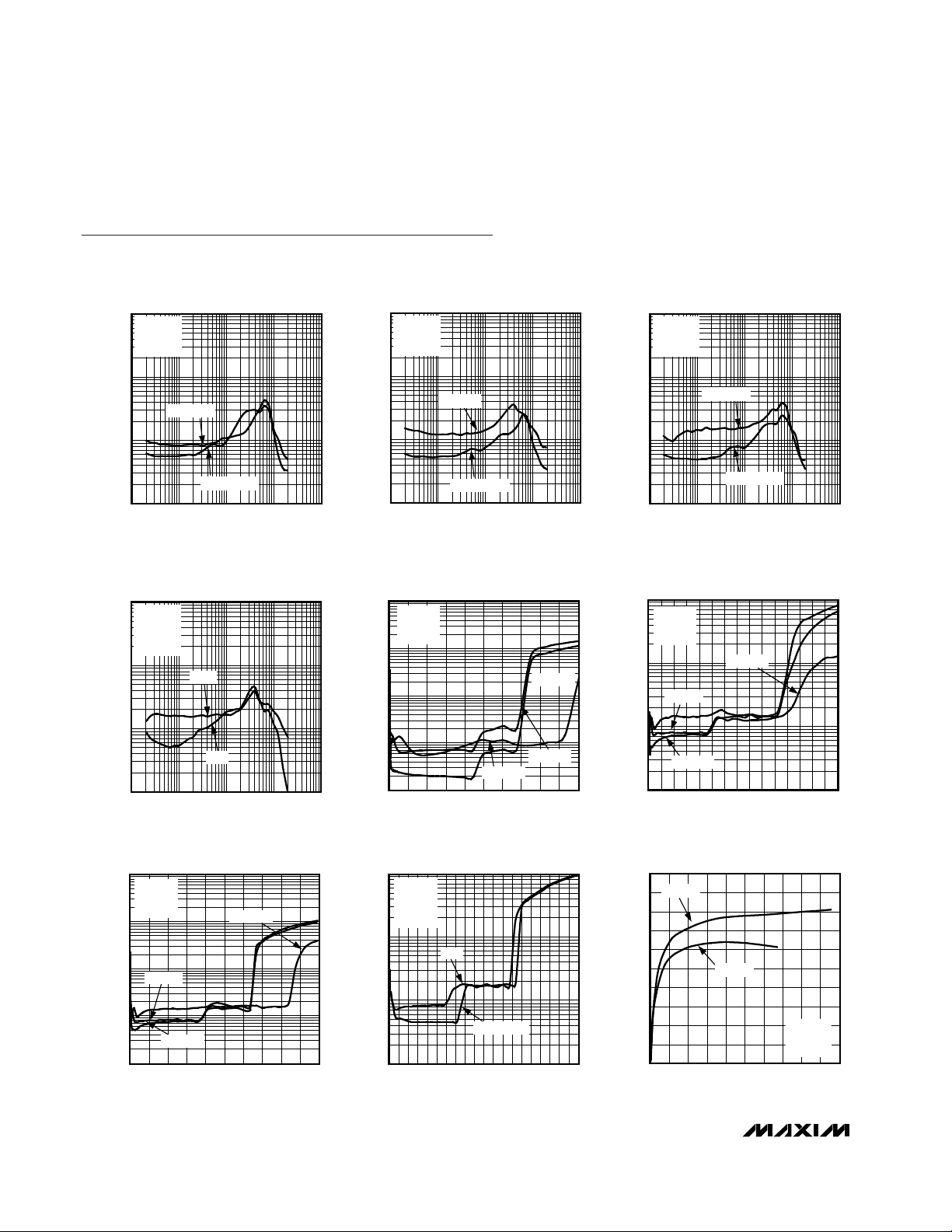
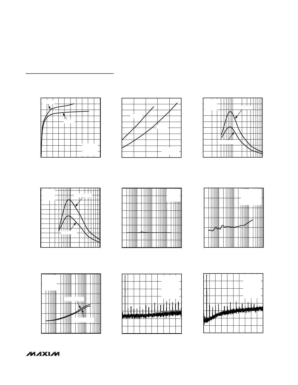
TOTAL HARMONIC DISTORTION PLUS
NOISE vs. FREQUENCY
MAX9703/04 toc01
FREQUENCY (Hz)
THD+N (%)
10k1k100
0.1
1
10
0.01
10 100k
VDD = 15V
R
L
= 4
Ω
A
V
= 16dB
P
OUT
= 4W
P
OUT
= 500mW
TOTAL HARMONIC DISTORTION PLUS
NOISE vs. FREQUENCY
MAX9703/04 toc02
FREQUENCY (Hz)
THD+N (%)
10k1k100
0.1
1
10
0.01
10 100k
VDD = 15V
R
L
= 8
Ω
A
V
= 16dB
P
OUT
= 500mW
P
OUT
= 8W
TOTAL HARMONIC DISTORTION PLUS
NOISE vs. FREQUENCY
MAX9703/04 toc03
FREQUENCY (Hz)
THD+N (%)
10k1k100
0.1
1
10
0.01
10 100k
VDD = 20V
R
L
= 8
Ω
A
V
= 16dB
P
OUT
= 8W
P
OUT
= 500mW
TOTAL HARMONIC DISTORTION PLUS
NOISE vs. FREQUENCY
MAX9703/04 toc04
FREQUENCY (Hz)
THD+N (%)
10k1k100
0.1
1
10
0.01
10 100k
VDD = 20V
R
L
= 8
Ω
A
V
= 16dB
P
OUT
= 8W
SSM
FFM
TOTAL HARMONIC DISTORTION PLUS
NOISE vs. OUTPUT POWER
MAX9703/04 toc07
OUTPUT POWER (W)
THD+N (%)
42681012 14 16 18
0.1
1
10
100
0.01
020
VDD = 20V
R
L
= 8
Ω
A
V
= 16dB
f = 100Hz
f = 1kHz
f = 10kHz
TOTAL HARMONIC DISTORTION PLUS
NOISE vs. OUTPUT POWER
MAX9703/04 toc05
OUTPUT POWER (W)
THD+N (%)
6
45
231
0.1
1
10
100
0.01
010978
VDD = 15V
R
L
= 4
Ω
A
V
= 16dB
f = 10kHz
f = 1kHz
f = 100Hz
TOTAL HARMONIC DISTORTION PLUS
NOISE vs. OUTPUT POWER
MAX9703/04 toc06
OUTPUT POWER (W)
THD+N (%)
12345678910 11 12 13 14
0.1
1
10
0.01
015
VDD = 15V
R
L
= 8
Ω
A
V
= 16dB
f = 100Hz
f = 1kHz
f = 10kHz
TOTAL HARMONIC DISTORTION PLUS
NOISE vs. OUTPUT POWER
MAX9703/04 toc08
OUTPUT POWER (W)
THD+N (%)
1234
5678
91011 12 13 141516 17 18 19
0.1
1
10
0.01
020
FFM (335kHz)
SSM
VDD = 20V
R
L
= 8
Ω
A
V
= 16dB
f = 1kHz
EFFICIENCY vs. OUTPUT POWER
MAX9703/04 toc09
OUTPUT POWER (W)
EFFICIENCY (%)
86423 5 7
9
1
10
20
30
40
50
60
70
80
90
100
0
010
VDD = 12V
A
V
= 16dB
f = 1kHz
RL = 4
Ω
RL = 8
Ω
Typical Operating Characteristics
(33µH with 4Ω, 68µH with 8Ω, part in SSM mode, 136µH with 16Ω, measurement BW = 22Hz to 22kHz, unless otherwise noted.)
Page 5
MAX9703/MAX9704
15W, Filterless, Spread-Spectrum
Mono/Stereo Class D Amplifiers
_______________________________________________________________________________________ 5
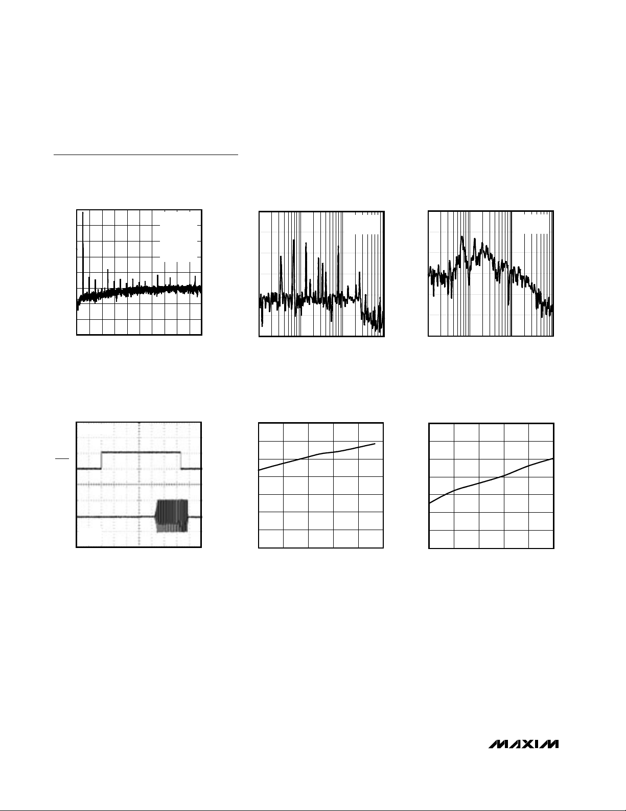
EFFICIENCY vs. OUTPUT POWER
MAX9703/04 toc10
OUTPUT POWER (W)
EFFICIENCY (%)
16
12
8
4
2
6
10
14 18
10
20
30
40
50
60
70
80
90
100
0
020
VDD = 15V
A
V
= 16dB
f = 1kHz
RL = 16
Ω
RL = 8
Ω
OUTPUT POWER
vs. SUPPLY VOLTAGE
MAX9703/04 toc11
SUPPLY VOLTAGE (V)
OUTPUT POWER (W)
0
6
4
2
8
10
12
14
16
18
20
10 1613 19 22 25
RL = 8
Ω
RL = 16
Ω
AV = 16dB
THD+N = 10%
20
18
16
14
12
10
8
6
4
2
0
110100
OUTPUT POWER
vs. LOAD RESISTANCE
MAX9703/04 toc12
LOAD RESISTANCE (Ω)
OUTPUT POWER (W)
THD+N = 1%
THD+N = 10%
VDD = 15V
R
L
= 8
Ω
A
V
= 16dB
24
22
20
18
16
14
12
10
8
6
4
2
0
110100
OUTPUT POWER
vs. LOAD RESISTANCE
MAX9703/04 toc13
LOAD RESISTANCE (Ω)
OUTPUT POWER (W)
VDD = 20V
R
L
= 8
Ω
A
V
= 16dB
THD+N = 10%
THD+N = 1%
CROSSTALK vs. FREQUENCY
MAX9703/04 toc16
FREQUENCY (Hz)
CROSSTALK (dB)
10k1k100
-80
-100
-60
-40
-20
0
-120
10 100k
LEFT TO RIGHT
RIGHT TO LEFT
AV = 16dB
1% THD+N
V
DD
= 15V
8Ω LOAD
COMMON-MODE REJECTION RATIO
vs. FREQUENCY
MAX9703/04 toc14
FREQUENCY (Hz)
CMRR (dB)
10k1k100
-70
-60
-50
-40
-30
-20
-10
0
-80
10 100k
VDD = 15V
R
L
= 8
Ω
A
V
= 16dB
POWER-SUPPLY REJECTION RATIO
vs. FREQUENCY
MAX9703/04 toc15
FREQUENCY (Hz)
PSRR (dB)
10k1k100
-100
-80
-60
-40
-20
0
-120
10 100k
AV = 16dB
R
L
= 8
Ω
200mV
P-P
INPUT
V
DD
= 15V
OUTPUT FREQUENCY SPECTRUM
MAX9703/04 toc17
FREQUENCY (kHz)
OUTPUT MAGNITUDE (dB)
-120
-100
-80
-60
-40
-20
0
20
-140
181612 144 6 8 102020
FFM MODE
A
V
= 16dB
UNWEIGHTED
f
IN
= 1kHz
P
OUT
= 5W
R
L
= 8
Ω
OUTPUT FREQUENCY SPECTRUM
MAX9703/04 toc18
FREQUENCY (kHz)
OUTPUT MAGNITUDE (dB)
-120
-100
-80
-60
-40
-20
0
20
-140
181612 144 6 8 102020
SSM MODE
A
V
= 16dB
UNWEIGHTED
f
IN
= 1kHz
P
OUT
= 5W
R
L
= 8
Ω
Typical Operating Characteristics (continued)
(33µH with 4Ω, 68µH with 8Ω, part in SSM mode, 136µH with 16Ω, measurement BW = 22Hz to 22kHz, unless otherwise noted.)
Page 6
MAX9703/MAX9704
15W, Filterless, Spread-Spectrum
Mono/Stereo Class D Amplifiers
6 _______________________________________________________________________________________
OUTPUT FREQUENCY SPECTRUM
MAX9703/04 toc19
FREQUENCY (kHz)
OUTPUT MAGNITUDE (dB)
-120
-100
-80
-60
-40
-20
0
20
-140
181612 144 6 8 102020
SSM MODE
A
V
= 16dB
A-WEIGHTED
f
IN
= 1kHz
P
OUT
= 5W
R
L
= 8
Ω
100k 1M 10M 100M
WIDEBAND OUTPUT SPECTRUM
(FFM MODE)
MAX9703/04 toc20
FREQUENCY (Hz)
OUTPUT AMPLITUDE (dBV)
0
-120
-100
-80
-60
-40
-20
RBW = 10kHz
V
DD
= 15V
100k 1M 10M 100M
WIDEBAND OUTPUT SPECTRUM
(SSM MODE)
MAX9703/04 toc21
FREQUENCY (Hz)
OUTPUT AMPLITUDE (dBV)
0
-120
-100
-80
-60
-40
-20
RBW = 10kHz
V
DD
= 15V
TURN-ON/TURN-OFF RESPONSE
MAX9703/04 toc22
20ms/div
OUTPUT
1V/div
5V/div
SHDN
f = 1kHz
R
L
= 8
Ω
CSS = 180pF
SUPPLY CURRENT
vs. SUPPLY VOLTAGE
MAX9703/04 toc23
SUPPLY VOLTAGE (V)
SUPPLY CURRENT (mA)
22191613
10
5
15
20
25
30
35
0
10 25
SHUTDOWN SUPPLY CURRENT
vs. SUPPLY VOLTAGE
MAX97703/04 toc24
SUPPLY VOLTAGE (V)
SUPPLY CURRENT (µA)
18161412
0.10
0.05
0.15
0.20
0.25
0.30
0.35
0
10 20
Typical Operating Characteristics (continued)
(33µH with 4Ω, 68µH with 8Ω, part in SSM mode, 136µH with 16Ω, measurement BW = 22Hz to 22kHz, unless otherwise noted.)
Page 7

MAX9703/MAX9704
15W, Filterless, Spread-Spectrum
Mono/Stereo Class D Amplifiers
_______________________________________________________________________________________ 7
PIN
MAX9703 MAX9704
NAME FUNCTION
1, 2, 23, 24 1, 2, 23, 24 PGND Power Ground
3, 4, 21, 22 3, 4, 21, 22 V
DD
Power-Supply Input
55C1N Charge-Pump Flying Capacitor Negative Terminal
66C1P Charge-Pump Flying Capacitor Positive Terminal
77
Charge-Pump Hold Capacitor. Connect a 1µF capacitor from CHOLD to VDD.
8, 17, 20, 25,
26, 31, 32
8N.C. No Connection. Not internally connected.
914REG Internal Regulator Output. Bypass with a 0.47µF capacitor to PGND.
10 13 AGND Analog Ground
11 — IN- Negative Input
12 — IN+ Positive Input
13 12 SS
Soft-Start. Connect a 0.47µF capacitor from SS to GND to enable soft-start feature.
14 11 SHDN
Active-Low Shutdown. Connect SHDN to GND to disable the device. Connect to
V
DD
for normal operation.
15 17 G1 Gain-Select Input 1
16 18 G2 Gain-Select Input 2
18 19 FS1 Frequency-Select Input 1
19 20 FS2 Frequency-Select Input 2
27, 28 — OUT- Negative Audio Output
29, 30 — OUT+ Positive Audio Output
—9INL- Left-Channel Negative Input
—10INL+ Left-Channel Positive Input
—15INR- Right-Channel Negative Input
—16INR+ Right-Channel Positive Input
— 25, 26 OUTR- Right-Channel Negative Audio Output
— 27, 28 OUTR+ Right-Channel Positive Audio Output
— 29, 30 OUTL- Left-Channel Negative Audio Output
— 31, 32 OUTL+ Left-Channel Positive Audio Output
——EP Exposed Paddle. Connect to GND.
Pin Description
CHOLD
Page 8

MAX9703/MAX9704
Detailed Description
The MAX9703/MAX9704 filterless, class D audio power
amplifiers feature several improvements to switchmode amplifier technology. The MAX9703 is a mono
amplifier, the MAX9704 is a stereo amplifier. These
devices offer class AB performance with class D efficiency, while occupying minimal board space. A
unique filterless modulation scheme and spread-spectrum switching mode create a compact, flexible, lownoise, efficient audio power amplifier. The differential
input architecture reduces common-mode noise pickup, and can be used without input-coupling capacitors.
The devices can also be configured as a single-ended
input amplifier.
Comparators monitor the device inputs and compare
the complementary input voltages to the triangle waveform. The comparators trip when the input magnitude of
the triangle exceeds their corresponding input voltage.
Operating Modes
Fixed-Frequency Modulation (FFM) Mode
The MAX9703/MAX9704 feature three FFM modes with
different switching frequencies (Table 1). In FFM mode,
the frequency spectrum of the class D output consists
of the fundamental switching frequency and its associated harmonics (see the Wideband FFT graph in the
Typical Operating Characteristics). The MAX9703/
MAX9704 allow the switching frequency to be changed
by ±35%, should the frequency of one or more of the
harmonics fall in a sensitive band. This can be done at
any time and does not affect audio reproduction.
Spread-Spectrum Modulation (SSM) Mode
The MAX9703/MAX9704 feature a unique, patented
spread-spectrum mode that flattens the wideband
spectral components, improving EMI emissions that
may be radiated by the speaker and cables. This mode
is enabled by setting FS1 = FS2 = H. In SSM mode, the
switching frequency varies randomly by ±7% around
the center frequency (670kHz). The modulation scheme
remains the same, but the period of the triangle waveform changes from cycle to cycle. Instead of a large
amount of spectral energy present at multiples of the
switching frequency, the energy is now spread over a
bandwidth that increases with frequency. Above a few
megahertz, the wideband spectrum looks like white
noise for EMI purposes.
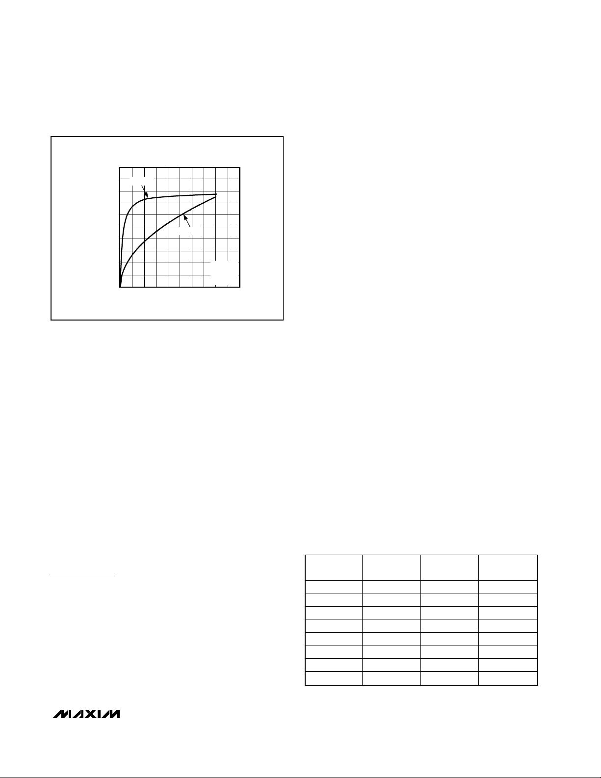
Efficiency
Efficiency of a class D amplifier is attributed to the
region of operation of the output stage transistors. In a
class D amplifier, the output transistors act as currentsteering switches and consume negligible additional
power. Any power loss associated with the class D output stage is mostly due to the I*R loss of the MOSFET
on-resistance, and quiescent current overhead.
The theoretical best efficiency of a linear amplifier is
78%; however, that efficiency is only exhibited at peak
output powers. Under normal operating levels (typical
music reproduction levels), efficiency falls below 30%,
whereas the MAX9704 still exhibits >78% efficiency
under the same conditions (Figure 2).
15W, Filterless, Spread-Spectrum
Mono/Stereo Class D Amplifiers
8 _______________________________________________________________________________________
Table 1. Operating Modes
FS1 FS2
SWITCHING MODE
(kHz)
LL 670
LH 940
HL 470
HH670 ±7%
Figure 1. MAX9704 Outputs with No Input Signal Applied
VIN = 0V
OUT-
OUT+
Page 9
Shutdown
The MAX9703/MAX9704 have a shutdown mode that
reduces power consumption and extends battery life.
Driving SHDN low places the device in low-power
(0.2µA) shutdown mode. Connect SHDN to a logic high
for normal operation.
Click-and-Pop Suppression
The MAX9703/MAX9704 feature comprehensive clickand-pop suppression that eliminates audible transients
on startup and shutdown. While in shutdown, the Hbridge is pulled to GND through 330kΩ. During startup,
or power-up, the input amplifiers are muted and an internal loop sets the modulator bias voltages to the correct
levels, preventing clicks and pops when the H-bridge is
subsequently enabled. Following startup, a soft-start
function gradually unmutes the input amplifiers. The
value of the soft-start capacitor has an impact on the
click/pop levels. For optimum performance, C
SS
should
be at least 180nF with a voltage rating of at least 7V.
Applications Information
Filterless Operation
Traditional class D amplifiers require an output filter to
recover the audio signal from the amplifier’s PWM output. The filters add cost, increase the solution size of
the amplifier, and can decrease efficiency. The traditional PWM scheme uses large differential output
swings (2
✕
VDDpeak-to-peak) and causes large ripple
currents. Any parasitic resistance in the filter components results in a loss of power, lowering the efficiency.
The MAX9703/MAX9704 do not require an output filter.
The devices rely on the inherent inductance of the
speaker coil and the natural filtering of both the speaker and the human ear to recover the audio component
of the square-wave output. Eliminating the output filter
results in a smaller, less-costly, more-efficient solution.
Because the frequency of the MAX9703/MAX9704 output is well beyond the bandwidth of most speakers,
voice coil movement due to the square-wave frequency
is very small. Although this movement is small, a speaker not designed to handle the additional power can be
damaged. For optimum results, use a speaker with a
series inductance > 30µH. Typical 8Ω speakers exhibit
series inductances in the range of 30µH to 100µH.
Optimum efficiency is achieved with speaker inductances > 60µH.
Gain Selection
Table 2 shows the suggested gain settings to attain a
maximum output power from a given peak input voltage
and given load.
Output Offset
Unlike a class AB amplifier, the output offset voltage of
class D amplifiers does not noticeably increase quiescent current draw when a load is applied. This is due to
the power conversion of the class D amplifier. For
example, an 8mVDC offset across an 8Ω load results in
1mA extra current consumption in a class AB device. In
the class D case, an 8mV offset into 8Ω equates
to an additional power drain of 8µW. Due to the high
efficiency of the class D amplifier, this represents an
additional quiescent current draw of: 8µW/(VDD/100 ✕ η),
which is in the order of a few microamps.
MAX9703/MAX9704
15W, Filterless, Spread-Spectrum
Mono/Stereo Class D Amplifiers
_______________________________________________________________________________________ 9
Figure 2. MAX9704 Efficiency vs. Class AB Efficiency
0
30
20
10
40
50
60
70
80
90
100
0
6
8
10 12 141618
24
20
EFFICIENCY vs. OUTPUT POWER
OUTPUT POWER (W)
EFFICIENCY (%)
VDD = 15V
f = 1kHz
R
L
= 8
Ω
MAX9704
CLASS AB
Table 2. Gain Settings
GAIN (dB)
INPUT DIFF
(V
RMS
)
R
L
(Ω)
P
OUT
AT 10%
THD+N (W)
13.0 0.67 4 9
16.0 0.48 4 9
19.1 0.33 4 9
29.6 0.10 4 9
13.0 1.23 8 15
16.0 0.86 8 15
19.1 0.61 8 15
29.6 0.19 8 15
Page 10

MAX9703/MAX9704
Input Amplifier
Differential Input
The MAX9703/MAX9704 feature a differential input structure, making them compatible with many CODECs, and
offering improved noise immunity over a single-ended
input amplifier. In devices such as PCs, noisy digital signals can be picked up by the amplifier’s input traces.
The signals appear at the amplifiers’ inputs as commonmode noise. A differential input amplifier amplifies the
difference of the two inputs, any signal common to both
inputs is canceled.
Single-Ended Input
The MAX9703/MAX9704 can be configured as singleended input amplifiers by capacitively coupling either
input to GND and driving the other input (Figure 3).
Component Selection
Input Filter
An input capacitor, C
IN
, in conjunction with the input
impedance of the MAX9703/MAX9704, forms a highpass filter that removes the DC bias from an incoming
signal. The AC-coupling capacitor allows the amplifier
to bias the signal to an optimum DC level. Assuming
zero-source impedance, the -3dB point of the highpass
filter is given by:
Choose C
IN
so f
-3dB
is well below the lowest frequency
of interest. Setting f
-3dB
too high affects the low-frequency response of the amplifier. Use capacitors with
dielectrics that have low-voltage coefficients, such as
tantalum or aluminum electrolytic. Capacitors with highvoltage coefficients, such as ceramics, may result in
increased distortion at low frequencies.
Charge-Pump Capacitor Selection
Use capacitors with an ESR less than 100mΩ for optimum performance. Low-ESR ceramic capacitors minimize the output resistance of the charge pump. For
best performance over the extended temperature
range, select capacitors with an X7R dielectric.
Flying Capacitor (C1)
The value of the flying capacitor (C1) affects the load
regulation and output resistance of the charge pump. A
C1 value that is too small degrades the device’s ability to
provide sufficient current drive. Increasing the value of
C1 improves load regulation and reduces the chargepump output resistance to an extent. Above 1µF, the onresistance of the switches and the ESR of C1 and C2
dominate.
Hold Capacitor (C2)
The output capacitor value and ESR directly affect the ripple at CHOLD. Increasing C2 reduces output ripple.
Likewise, decreasing the ESR of C2 reduces both ripple
and output resistance. Lower capacitance values can be
used in systems with low maximum output power levels.
Output Filter
The MAX9703/MAX9704 do not require an output filter
and can pass FCC emissions standards with unshielded speaker cables. However, output filtering can be
used if a design is failing radiated emissions due to
board layout or cable length, or the circuit is near EMIsensitive devices. Use a ferrite bead filter when radiated frequencies above 10MHz are of concern. Use an
LC filter when radiated frequencies below 10MHz are of
concern, or when long leads connect the amplifier to
the speaker. Refer to the MAX9704 Evaluation Kit
schematic for details of this filter.
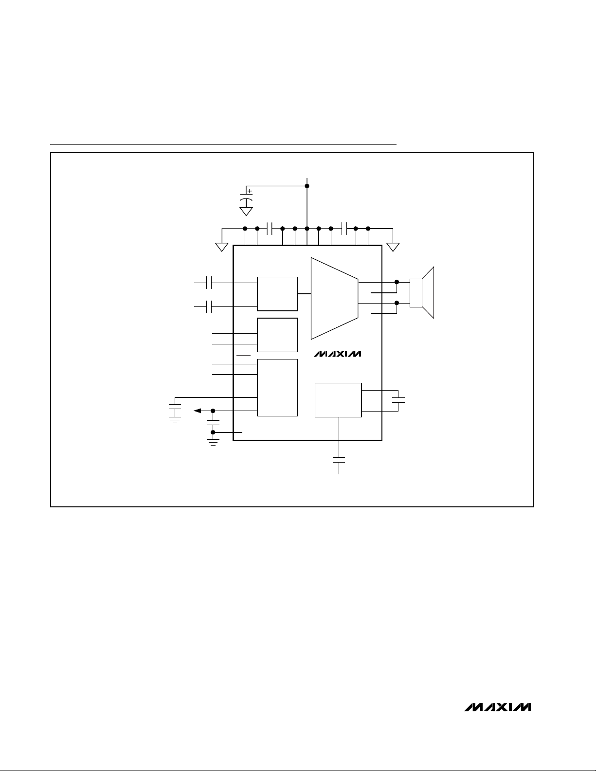
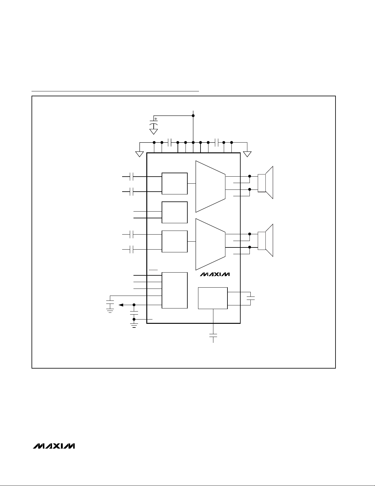
Sharing Input Sources
In certain systems, a single audio source can be shared
by multiple devices (speaker and headphone amplifiers). When sharing inputs, it is common to mute the
unused device, rather than completely shutting it down,
preventing the unused device inputs from distorting the
input signal. Mute the MAX9703/MAX9704 by driving SS
low through an open-drain output or MOSFET (see the
System Diagram). Driving SS low turns off the class D
output stage, but does not affect the input bias levels of
the MAX9703/MAX9704. Be aware that during normal
operation, the voltage at SS can be up to 7V, depending
on the MAX9703/MAX9704 supply.
f
RC
-3dB
IN IN
1
2=π
15W, Filterless, Spread-Spectrum
Mono/Stereo Class D Amplifiers
10 ______________________________________________________________________________________
MAX9703/
MAX9704
IN+
IN-
0.47µF
0.47µF
SINGLE-ENDED
AUDIO INPUT
Figure 3. Single-Ended Input
Page 11

Supply Bypassing/Layout
Proper power-supply bypassing ensures low distortion
operation. For optimum performance, bypass VDDto
PGND with a 0.1µF capacitor as close to each V
DD
pin
as possible. A low-impedance, high-current power-sup-
ply connection to VDDis assumed. Additional bulk
capacitance should be added as required depending on
the application and power-supply characteristics. AGND
and PGND should be star connected to system ground.
Refer to the MAX9704 Evaluation Kit for layout guidance.
MAX9703/MAX9704
15W, Filterless, Spread-Spectrum
Mono/Stereo Class D Amplifiers
______________________________________________________________________________________ 11
32
31
30
29
28
27
26
N.C.
N.C.
OUT+
OUT+
OUT-
OUT-
N.C.
25 N.C.
9
10
11
12
13
14
15
REG
AGND
IN-
IN+
SS
G1
16G2
17
18
19
20
21
22
23
N.C.
FS1
FS2
N.C.
V
DD
V
DD
PGND
8
7
6
5
4
3
2
N.C.
CHOLD
C1P
C1N
V
DD
V
DD
PGND
MAX9703
1PGND
24 PGND
TOP VIEW
TQFN (5mm x 5mm)
SHDN
32
31
30
29
28
27
26
OUTL+
OUTL+
OUTL-
OUTL-
OUTR+
OUTR+
OUTR-
25 OUTR-
9
10
11
12
13
14
15
INL-
INL+
SS
AGND
INR-
REG
16INR+
17
18
19
20
21
22
23
G1
G2
FS1
FS2
V
DD
V
DD
PGND
8
7
6
5
4
3
2
N.C.
CHOLD
C1P
C1N
V
DD
V
DD
PGND
MAX9704
1PGND
24 PGND
TQFN (7mm x 7mm)
SHDN
Pin Configurations
Chip Information
MAX9703 TRANSISTOR COUNT: 3093
MAX9704 TRANSISTOR COUNT: 4630
PROCESS: BiCMOS
Page 12
MAX9703/MAX9704
15W, Filterless, Spread-Spectrum
Mono/Stereo Class D Amplifiers
12 ______________________________________________________________________________________
MAX9703
0.47µF
LOGIC INPUTS SHOWN FOR A
V
= 16dB (SSM).
V
IN
= LOGIC HIGH > 2.5V.
IN+11
12
18
14
15
16
13
10 AGND
9
6
5
19
IN-
FS1
V
REG
V
REG
V
REG
V
REG
FS2
G1
G2
SS
REG
V
REG
0.47µF
MODULATOR
OSCILLATOR
CHARGE PUMP
C1P
C1
0.1µF
25V
C1N
0.18µF
10V
V
IH
GAIN
CONTROL
SHUTDOWN
CONTROL
0.47µF
10V
SHDN
H-BRIDGE
OUT+
OUT+
OUTOUT-
30
29
28
27
PGND V
DD
V
DD
PGND
134212223242
10V TO 25V
100µF
25V
0.1µF
25V
0.1µF
25V
C2
1µF
25V
CHOLD
V
DD
7
Functional Diagrams
Page 13
MAX9703/MAX9704
15W, Filterless, Spread-Spectrum
Mono/Stereo Class D Amplifiers
______________________________________________________________________________________ 13
MAX9704
0.47µF
LOGIC INPUTS SHOWN FOR A
V
= 16dB (SSM).
V
IN
= LOGIC HIGH > 2.5V.
INL+10
9
19
11
17
18
12
13 AGND
14
6
5
20
INL-
FS1
V
REG
V
REG
V
REG
V
REG
FS2
G1
G2
SS
REG
0.47µF
MODULATOR
OSCILLATOR
CHARGE PUMP
C1P
C1
0.1µF
25V
C1N
0.18µF
10V
V
IH
GAIN
CONTROL
SHUTDOWN
CONTROL
0.47µF
10V
SHDN
H-BRIDGE
OUTL+
OUTL+
OUTLOUTL-
32
31
30
29
PGND V
DD
V
DD
PGND
134212223242
10V TO 25V
100µF
25V
0.1µF
25V
0.1µF
25V
C2
1µF
25V
CHOLD
V
DD
7
0.47µF
INR+15
16
INR-
0.47µF
MODULATOR
H-BRIDGE
OUTR+
OUTR+
OUTROUTR-
26
25
28
27
V
REG
Functional Diagrams (continued)
Page 14

MAX9703/MAX9704
15W, Filterless, Spread-Spectrum
Mono/Stereo Class D Amplifiers
14 ______________________________________________________________________________________
MAX9704
MAX9722B
0.47µF
V
DD
INL-
V
DD
OUTL-
SHDN
OUTL+INL+
CODEC
INR+ OUTR+
OUTR-
0.18µF
5V
V
DD
OUTL
OUTR
PV
SS
SV
SS
INL+
INL-
INR+
INR-
C1P
1µF
1µF
CIN
100kΩ
INR-
0.47µF
0.47µF
0.47µF
1µF
SS
SHDN
LOGIC INPUTS SHOWN FOR AV = 16dB (SSM).
1µF
1µF
30kΩ 30kΩ
15kΩ
15kΩ
1µF
1µF
1µF
100µF
System Diagram
Page 15

MAX9703/MAX9704
15W, Filterless, Spread-Spectrum
Mono/Stereo Class D Amplifiers
______________________________________________________________________________________ 15
32, 44, 48L QFN.EPS
PROPRIETARY INFORMATION
APPROVAL
TITLE:
DOCUMENT CONTROL NO.
21-0144
PACKAGE OUTLINE
32, 44, 48, 56L THIN QFN, 7x7x0.8mm
1
D
REV.
2
e
L
e
L
A1AA2
E/2
E
D/2
D
DETAIL A
D2/2
D2
b
L
k
E2/2
E2
(NE-1) X e
(ND-1) X e
e
C
L
C
L
C
L
C
L
k
DALLAS
SEMICONDUCTOR
DETAIL B
e
L
L1
Package Information
(The package drawing(s) in this data sheet may not reflect the most current specifications. For the latest package outline information,
go to www.maxim-ic.com/packages
.)
Page 16

MAX9703/MAX9704
15W, Filterless, Spread-Spectrum
Mono/Stereo Class D Amplifiers
16 ______________________________________________________________________________________
PROPRIETARY INFORMATION
DOCUMENT CONTROL NO.APPROVAL
TITLE:
REV.
2
2
21-0144
DALLAS
SEMICONDUCTOR
PACKAGE OUTLINE
32, 44, 48, 56L THIN QFN, 7x7x0.8mm
D
Package Information (continued)
(The package drawing(s) in this data sheet may not reflect the most current specifications. For the latest package outline information,
go to www.maxim-ic.com/packages
.)
Page 17

MAX9703/MAX9704
15W, Filterless, Spread-Spectrum
Mono/Stereo Class D Amplifiers
______________________________________________________________________________________ 17
QFN THIN.EPS
D2
(ND-1) X e
e
D
C
PIN # 1
I.D.
(NE-1) X e
E/2
E
0.08 C
0.10 C
A
A1 A3
DETAIL A
0.15
C B
0.15 C A
E2/2
E2
0.10 M C A B
PIN # 1 I.D.
b
0.35x45∞
L
D/2
D2/2
L
C
L
C
e e
L
CC
L
k
k
LL
E
1
2
21-0140
PACKAGE OUTLINE
16, 20, 28, 32, 40L, THIN QFN, 5x5x0.8mm
DETAIL B
L
L1
e
Package Information (continued)
(The package drawing(s) in this data sheet may not reflect the most current specifications. For the latest package outline information,
go to www.maxim-ic.com/packages
.)
Page 18

MAX9703/MAX9704
15W, Filterless, Spread-Spectrum
Mono/Stereo Class D Amplifiers
Maxim cannot assume responsibility for use of any circuitry other than circuitry entirely embodied in a Maxim product. No circuit patent licenses are
implied. Maxim reserves the right to change the circuitry and specifications without notice at any time.
18 ____________________Maxim Integrated Products, 120 San Gabriel Drive, Sunnyvale, CA 94086 408-737-7600
© 2004 Maxim Integrated Products Printed USA is a registered trademark of Maxim Integrated Products.
COMMON DIMENSIONS
3.353.15
T2855-1 3.25 3.353.15 3.25
MAX.
3.20
EXPOSED PAD VARIATIONS
3.00T2055-2 3.10
D2
NOM.MIN.
3.203.00 3.10
MIN.E2NOM. MAX.
NE
ND
PKG.
CODES
1. DIMENSIONING & TOLERANCING CONFORM TO ASME Y14.5M-1994.
2. ALL DIMENSIONS ARE IN MILLIMETERS. ANGLES ARE IN DEGREES.
3. N IS THE TOTAL NUMBER OF TERMINALS.
4. THE TERMINAL #1 IDENTIFIER AND TERMINAL NUMBERING CONVENTION SHALL CONFORM TO JESD 95-1
SPP-012. DETAILS OF TERMINAL #1 IDENTIFIER ARE OPTIONAL, BUT MUST BE LOCATED WITHIN THE
ZONE INDICATED. THE TERMINAL #1 IDENTIFIER MAY BE EITHER A MOLD OR MARKED FEATURE.
5. DIMENSION b APPLIES TO METALLIZED TERMINAL AND IS MEASURED BETWEEN 0.25 mm AND 0.30 mm
FROM TERMINAL TIP.
6. ND AND NE REFER TO THE NUMBER OF TERMINALS ON EACH D AND E SIDE RESPECTIVELY.
7. DEPOPULATION IS POSSIBLE IN A SYMMETRICAL FASHION.
8. COPLANARITY APPLIES TO THE EXPOSED HEAT SINK SLUG AS WELL AS THE TERMINALS.
9. DRAWING CONFORMS TO JEDEC MO220, EXCEPT EXPOSED PAD DIMENSION FOR T2855-1,
T2855-3 AND T2855-6.
NOTES:
SYMBOL
PKG.
N
L1
e
E
D
b
A3
A
A1
k
10. WARPAGE SHALL NOT EXCEED 0.10 mm.
JEDEC
T1655-1
3.203.00 3.10 3.00 3.10 3.20
0.70 0.800.75
4.90
4.90
0.25
0.250--
4
WHHB
4
16
0.350.30
5.10
5.105.00
0.80 BSC.
5.00
0.05
0.20 REF.
0.02
MIN. MAX.NOM.
16L 5x5
3.10
T3255-2
3.00
3.20
3.00 3.10 3.20
2.70
T2855-2 2.60 2.602.80 2.70 2.80
E
2
2
21-0140
PACKAGE OUTLINE
16, 20, 28, 32, 40L, THIN QFN, 5x5x0.8mm
L
0.30 0.500.40
---
---
WHHC
20
5
5
5.00
5.00
0.30
0.55
0.65 BSC.
0.45
0.25
4.90
4.90
0.25
0.65
--
5.10
5.10
0.35
20L 5x5
0.20 REF.
0.75
0.02
NOM.
0
0.70
MIN.
0.05
0.80
MAX.
---
WHHD-1
28
7
7
5.00
5.00
0.25
0.55
0.50 BSC.
0.45
0.25
4.90
4.90
0.20
0.65
--
5.10
5.10
0.30
28L 5x5
0.20 REF.
0.75
0.02
NOM.
0
0.70
MIN.
0.05
0.80
MAX.
---
WHHD-2
32
8
8
5.00
5.00
0.40
0.50 BSC.
0.30
0.25
4.90
4.90
0.50
--
5.10
5.10
32L 5x5
0.20 REF.
0.75
0.02
NOM.
0
0.70
MIN.
0.05
0.80
MAX.
-
40
10
10
5.00
5.00
0.20
0.50
0.40 BSC.
0.40
0.25
4.90
4.90
0.15
0.60
5.10
5.10
0.25
40L 5x5
0.20 REF.
0.75
NOM.
0
0.70
MIN.
0.05
0.80
MAX.
0.20 0.25 0.30
-
0.35 0.45
0.30 0.40 0.50
DOWN
BONDS
ALLOWED
NO
YES3.103.00 3.203.103.00 3.20T2055-3
3.103.00 3.203.103.00 3.20T2055-4
T2855-3 3.15 3.25 3.35 3.15 3.25 3.35
T2855-6 3.15 3.25 3.35 3.15 3.25 3.35
T2855-4 2.60 2.70 2.80 2.60 2.70 2.80
T2855-5 2.60 2.70 2.80 2.60 2.70 2.80
T2855-7 2.60 2.70
2.80
2.60 2.70 2.80
3.20
3.00 3.10T3255-3 3.203.00 3.10
3.203.00 3.10T3255-4 3.203.00 3.10
3.403.20 3.30T4055-1 3.20 3.30 3.40
NO
NO
NO
NO
NO
NO
NO
NO
YES
YES
YES
YES
YES
3.203.00T1655-2 3.10 3.00 3.10 3.20 YE S
Package Information (continued)
(The package drawing(s) in this data sheet may not reflect the most current specifications. For the latest package outline information,
go to www.maxim-ic.com/packages
.)
 Loading...