

Page 1
General Description
The MAX9700 mono class D audio power amplifier provides class AB amplifier performance with class D efficiency, conserving board space and extending battery
life. Using a class D architecture, the MAX9700 delivers
1.2W into an 8Ω load while offering efficiencies above
90%. A patented, low-EMI modulation scheme renders
the traditional class D output filter unnecessary.
The MAX9700 offers two modulation schemes: a fixedfrequency (FFM) mode, and a spread-spectrum (SSM)
mode that reduces EMI-radiated emissions due to the
modulation frequency. Furthermore, the MAX9700 oscillator can be synchronized to an external clock through
the SYNC input, allowing the switching frequency to be
user defined. The SYNC input also allows multiple
MAX9700s to be cascaded and frequency locked, minimizing interference due to clock intermodulation. The
device utilizes a fully differential architecture, a fullbridged output, and comprehensive click-and-pop suppression. The gain of the MAX9700 is set internally
(MAX9700A: 6dB, MAX9700B: 12dB, MAX9700C:
15.6dB, MAX9700D: 20dB), further reducing external
component count.
The MAX9700 features high 72dB PSRR, a low 0.01%
THD+N, and SNR in excess of 90dB. Short-circuit and
thermal-overload protection prevent the device from
damage during a fault condition. The MAX9700 is available in 10-pin TDFN (3mm ✕3mm ✕0.8mm), 10-pin
µMAX, and 12-bump UCSP™ (1.5mm ✕2mm ✕ 0.6mm)
packages. The MAX9700 is specified over the extended
-40°C to +85°C temperature range.
Applications
Features
♦ Filterless Amplifier Passes FCC Radiated
Emissions Standards with 100mm of Cable
♦ Unique Spread-Spectrum Mode Offers 5dB
Emissions Improvement Over Conventional
Methods
♦ Optional External SYNC Input
♦ Simple Master-Slave Setup for Stereo Operation
♦ 94% Efficiency
♦ 1.2W into 8Ω
♦ Low 0.01% THD+N
♦ High PSRR (72dB at 217Hz)
♦ Integrated Click-and-Pop Suppression
♦ Low Quiescent Current (4mA)
♦ Low-Power Shutdown Mode (0.1µA)
♦ Short-Circuit and Thermal-Overload Protection
♦ Available in Thermally Efficient, Space-Saving
Packages
10-Pin TDFN (3mm ✕ 3mm ✕ 0.8mm)
10-Pin µMAX
12-Bump UCSP (1.5mm ✕2mm ✕0.6mm)
MAX9700
1.2W, Low-EMI, Filterless,
Class D Audio Amplifier
________________________________________________________________ Maxim Integrated Products 1
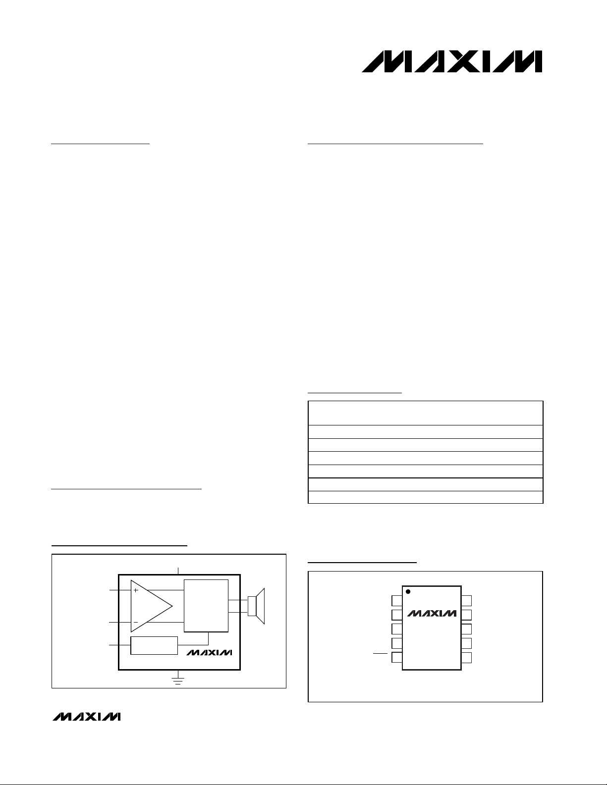
Pin Configurations
Ordering Information
MAX9700
DIFFERENTIAL
AUDIO INPUT
SYNC
INPUT
V
DD
OSCILLATOR
MODULATOR
AND H-BRIDGE
Block Diagram
19-3030; Rev 0; 10/03
For pricing, delivery, and ordering information, please contact Maxim/Dallas Direct! at
1-888-629-4642, or visit Maxim’s website at www.maxim-ic.com.
Cellular Phones
PDAs
MP3 Players
Portable Audio
Pin Configurations continued at end of data sheet.
Ordering Information continued at end of data sheet.
*Future Product—contact factory for availability.
UCSP is a trademark of Maxim Integrated Products, Inc.
Selector Guide appears at end of data sheet.
PART TEMP RANGE
o
MAX9700AETB* -40
MAX9700AEUB* -40oC to +85oC 10 µMAX —
MAX9700AEBC-T* -40oC to +85oC 12 UCSP-12 —
MAX9700BETB -40oC to +85oC 10 TDFN ACI
MAX9700BEUB* -40oC to +85oC 10 µMAX —
MAX9700BEBC-T* -40oC to +85oC 12 UCSP-12 —
C to +85oC 10 TDFN ACM
PINPACKAGE
TOP
MARK
TOP VIEW
V
1
DD
IN+
2
IN-
MAX9700
3
4
5
TDFN/µMAX
10
PV
DD
OUT-
9
OUT+
8
PGNDGND
7
SYNCSHDN
6
Page 2
1.2W, Low-EMI, Filterless,
Class D Audio Amplifier
2 _______________________________________________________________________________________
ABSOLUTE MAXIMUM RATINGS
ELECTRICAL CHARACTERISTICS
(VDD= PVDD= SHDN = 3.3V, GND = PGND = 0V, SYNC = GND (FFM), RL= 8Ω, RLconnected between OUT+ and OUT-
(MAX9700B), T
A
= T
MIN
to T
MAX
, unless otherwise noted. Typical values are at TA= +25°C.) (Notes 1, 2)
Stresses beyond those listed under “Absolute Maximum Ratings” may cause permanent damage to the device. These are stress ratings only, and functional
operation of the device at these or any other conditions beyond those indicated in the operational sections of the specifications is not implied. Exposure to
absolute maximum rating conditions for extended periods may affect device reliability.
VDDto GND..............................................................................6V
PV
DD
to PGND .........................................................................6V
GND to PGND .......................................................-0.3V to +0.3V
All Other Pins to GND.................................-0.3V to (V
DD
+ 0.3V)
Continuous Current Into/Out of PV
DD
/PGND/OUT_........±600mA
Continuous Input Current (all other pins)..........................±20mA
Duration of OUT_ Short Circuit to GND or PV
DD
........Continuous
Duration of Short Circuit Between OUT+ and OUT- ..Continuous
Continuous Power Dissipation (T
A
= +70°C)
10-Pin TDFN (derate 24.4mW/°C above +70°C) .....1951.2mW
10-Pin µMAX (derate 5.6mW/
o
C above +70°C) .........444.4mW
12-Bump UCSP (derate 6.1mW/°C above +70°C)........484mW
Junction Temperature......................................................+150°C
Operating Temperature Range ...........................-40°C to +85°C
Storage Temperature Range .............................-65°C to +150°C
Lead Temperature (soldering, 10s) .................................+300°C
Bump Temperature (soldering)
Reflow ..........................................................................+235°C
MAX9700
GENERAL
Supply Voltage Range V
Quiescent Current I
Shutdown Current I
Turn-On Time t
Input Resistance R
Input Bias Voltage V
Voltage Gain A
Output Offset Voltage V
Common-Mode Rejection Ratio CMRR fIN = 1kHz, input referred 72 dB
Power-Supply Rejection Ratio
(Note 3)
Output Power P
Total Harmonic Distortion
Plus Noise
PARAMETER SYMBOL CONDITIONS MIN TYP MAX UNITS
DD
DD
SHDN
ON
BIAS
OS
PSRR
OUT
THD+N
Inferred from PSRR test 2.5 5.5 V
TA = +25°C1420kΩ
IN
Either input 0.73 0.83 0.93 V
MAX9700A 6
MAX9700B 12
V
MAX9700C 15.6
MAX9700D 20
TA = +25°C ±11 40
T
≤ TA ≤ T
MIN
VDD = 2.5V to 5.5V 50 70
200mV
THD+N = 1%
f
= 1kHz, either
IN
FFM or SSM
P-P
MAX
ripple
f
= 217Hz 72
RIPPLE
= 20kHz 55
f
RIPPLE
RL = 8Ω 600
= 6Ω 800
R
L
RL = 8Ω,
P
= 125mW
OUT
R
= 6Ω,
L
P
= 125mW
OUT
4 5.2 mA
0.1 5 µA
30 ms
±65
0.01
0.01
dB
mV
dB
mW
%
Page 3
MAX9700
1.2W, Low-EMI, Filterless,
Class D Audio Amplifier
_______________________________________________________________________________________ 3
ELECTRICAL CHARACTERISTICS (continued)
(VDD= PVDD= SHDN = 3.3V, GND = PGND = 0V, SYNC = GND (FFM), RL= 8Ω, RLconnected between OUT+ and OUT-
(MAX9700B), T
A
= T
MIN
to T
MAX
, unless otherwise noted. Typical values are at TA= +25°C.) (Notes 1, 2)
Note 1: All devices are 100% production tested at +25°C. All temperature limits are guaranteed by design.
Note 2: Testing performed with a resistive load in series with an inductor to simulate an actual speaker load. For R
L
= 6Ω, L = 47µH.
For R
L
= 8Ω, L = 68µH. For RL= 16Ω, L = 136µH.
Note 3: PSRR is specified with the amplifier inputs connected to GND through C
IN
.
ELECTRICAL CHARACTERISTICS
(VDD= PVDD= SHDN = 5V, GND = PGND = 0V, SYNC = GND (FFM), RL= 8Ω, RLconnected between OUT+ and OUT-
(MAX9700B), T
A
= T
MIN
to T
MAX
, unless otherwise noted. Typical values are at TA= +25°C.) (Notes 1, 2)
Signal-to-Noise Ratio SNR V
Oscillator Frequency f
SYNC Frequency Lock Range 800 2000 kHz
Efficiency η P
DIGITAL INPUTS (SHDN, SYNC)
Input Thresholds
SHDN Input Leakage Current ±1µA
SYNC Input Current ±5µA
PARAMETER SYMBOL CONDITIONS MIN TYP MAX UNITS
FFM 89
SSM 87
FFM 92
SSM 90
OSC
BW = 22Hz
= 2V
OUT
SYNC = GND 980 1100 1220
SYNC = float 1280 1450 1620
SYNC = VDD (SSM mode)
OUT
V
IH
V
IL
RMS
= 500mW, fIN = 1kHz 94 %
to 22kHz
A-weighted
dB
1220
±120
2
0.8
kHz
V
Quiescent Current I
Shutdown Current I
Common-Mode Rejection Ratio CMRR f = 1kHz, input referred 72 dB
Power-Supply Rejection Ratio PSRR 200mV
Total Harmonic Distortion
Plus Noise
Signal-to-Noise Ratio SNR
PARAMETER SYMBOL CONDITIONS MIN TYP MAX UNITS
DD
SHDN
f = 217Hz 72
f = 20kHz 55
RL = 16Ω 700
RL = 8Ω 1200Output Power P
= 6Ω 1600
R
L
RL = 8Ω, P
R
= 4Ω, P
L
BW = 22Hz to
22kHz
A-weighted
= 125mW 0.015
OUT
= 125mW 0.02
OUT
FFM 92.5
SSM 90.5
FFM 95.5
SSM 93.5
OUT
THD+N
ripple
P-P
THD+N = 1%
f = 1kHz, either
FFM or SSM
V
=
OUT
3V
RMS
5.2 mA
0.1 µA
dB
mW
%
dB
Page 4
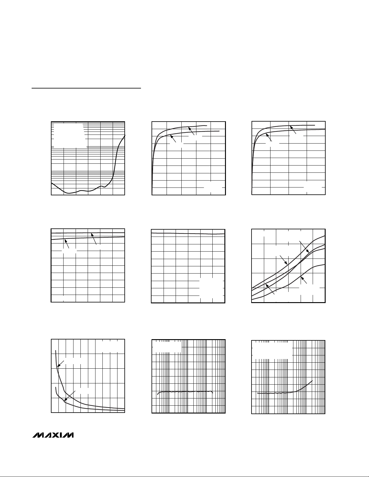
100
0 0.5 1.0 1.5 2.0
10
1
0.1
0.01
0.001
TOTAL HARMONIC DISTORTION PLUS NOISE
vs. OUTPUT POWER
MAX9700 toc04
OUTPUT POWER (W)
THD+N (%)
VDD = 5V
R
L
= 8Ω
f = 1kHz
f = 10kHz
f = 100Hz
100
0 0.2 0.4 0.6 0.8 1.0
10
1
0.1
0.01
0.001
TOTAL HARMONIC DISTORTION PLUS NOISE
vs. OUTPUT POWER
MAX9700 toc05
OUTPUT POWER (W)
THD+N (%)
VDD = 5V
R
L
= 16Ω
f = 10kHz
f = 1kHz
f = 100Hz
100
0 0.5 1.0 1.5 2.0
10
1
0.1
0.01
0.001
TOTAL HARMONIC DISTORTION PLUS NOISE
vs. OUTPUT POWER
MAX9700 toc06
OUTPUT POWER (W)
THD+N (%)
VDD = 5V
R
L
= 6Ω
f = 1kHz
f = 10kHz
f = 100Hz
100
0 0.1 0.2 0.3 0.4 0.5
10
1
0.1
0.01
0.001
TOTAL HARMONIC DISTORTION PLUS NOISE
vs. OUTPUT POWER
MAX9700 toc07
OUTPUT POWER (W)
THD+N (%)
VDD = 2.5V
R
L
= 8Ω
V
CM
= 1.25V
NO INPUT CAPACITORS
DIFFERENTIAL
INPUT
SINGLE ENDED
100
0 0.5 1.0 1.5 2.0
10
1
0.1
0.01
0.001
TOTAL HARMONIC DISTORTION PLUS NOISE
vs. OUTPUT POWER
MAX9700 toc08
OUTPUT POWER (W)
THD+N (%)
VDD = 5V
f = 1kHz
R
L
= 8Ω
FFM
(SYNC FLOATING)
SSM
FFM
(SYNC = GND)
100
0 0.5 1.0 1.5 2.0
10
1
0.1
0.01
0.001
TOTAL HARMONIC DISTORTION PLUS NOISE
vs. OUTPUT POWER
MAX9700 toc09
OUTPUT POWER (W)
THD+N (%)
VDD = 5V
f = 1kHz
R
L
= 8Ω
f
SYNC
= 800kHz
f
SYNC
= 2MHz
f
SYNC
= 1.4MHz
MAX9700
1.2W, Low-EMI, Filterless,
Class D Audio Amplifier
4 _______________________________________________________________________________________
Typical Operating Characteristics
(VDD= 3.3V, SYNC = GND (SSM), TA= +25°C, unless otherwise noted.)
0.001
10 100k10k100 1k
TOTAL HARMONIC DISTORTION PLUS NOISE
vs. FREQUENCY
1
0.1
0.01
MAX9700 toc01
FREQUENCY (Hz)
THD+N (%)
VDD = +5V
R
L
= 8Ω
P
OUT
= 300mW
P
OUT
= 125mW
0.001
10 100k10k100 1k
TOTAL HARMONIC DISTORTION PLUS NOISE
vs. FREQUENCY
1
0.1
0.01
MAX9700 toc02
FREQUENCY (Hz)
THD+N (%)
VDD = +3.3V
R
L
= 8Ω
P
OUT
= 300mW
P
OUT
= 125mW
0.001
10 100k10k100 1k
TOTAL HARMONIC DISTORTION PLUS NOISE
vs. FREQUENCY
1
0.1
0.01
MAX9700 toc03
FREQUENCY (Hz)
THD+N (%)
VDD = +3.3V
R
L
= 8Ω
P
OUT
= 125mW
SSM MODE
FFM MODE
Page 5
MAX9700
1.2W, Low-EMI, Filterless,
Class D Audio Amplifier
_______________________________________________________________________________________ 5
Typical Operating Characteristics (continued)
(VDD= 3.3V, SYNC = GND (SSM), TA= +25°C, unless otherwise noted.)
10
0 0.5 1.0 1.5 2.0 2.5 3.0
1
0.1
0.01
TOTAL HARMONIC DISTORTION PLUS NOISE
vs. COMMON-MODE VOLTAGE
MAX9700 toc10
COMMON-MODE VOLTAGE (V)
THD+N (%)
VDD = 3.3V
R
L
= 8Ω
f = 1kHz
P
OUT
= 300mW
DIFFERENTIAL INPUT
EFFICIENCY vs. OUTPUT POWER
MAX9700toc11
OUTPUT POWER (W)
EFFICIENCY (%)
0.80.60.40.2
10
20
30
40
50
60
70
80
90
100
0
0 1.0
RL = 6Ω
RL = 8Ω
VDD = 3.3V
f = 1kHz
EFFICIENCY vs. OUTPUT POWER
MAX9700toc12
OUTPUT POWER (W)
EFFICIENCY (%)
1.51.00.5
10
20
30
40
50
60
70
80
90
100
0
0 2.0
RL = 6Ω
RL = 8Ω
VDD = 5V
f = 1kHz
0
30
20
10
50
40
90
80
70
60
100
2.5 3.0 3.5 4.0 4.5 5.0 5.5
EFFICIENCY vs. SUPPLY VOLTAGE
MAX9700 toc13
SUPPLY VOLTAGE (V)
EFFICIENCY (%)
RL = 8Ω
f = 1kHz
RL = 6Ω
0
30
20
10
50
40
90
80
70
60
100
800 1000 1200 1400 18001600 2000
EFFICIENCY
vs. SYNC INPUT FREQUENCY
MAx9700 toc14
SYNC FREQUENCY (kHz)
EFFICIENCY (%)
VDD = 3.3V
f = 1kHz
P
OUT
= 300mW
R
L
= 8Ω
OUTPUT POWER vs.
SUPPLY VOLTAGE
MAX9700toc15
SUPPLY VOLTAGE (V)
OUTPUT POWER (mW)
5.04.54.03.53.0
500
1000
1500
2000
2500
0
2.5 5.5
RL = 6Ω
THD+N = 1%
f = 1kHz
RL = 6Ω
THD+N = 10%
RL = 8Ω
THD+N = 10%
RL = 8Ω
THD+N = 1%
OUTPUT POWER vs. LOAD RESISTANCE
MAX9700toc16
LOAD RESISTANCE (Ω)
OUTPUT POWER (mW)
908070605040302010
400
800
1200
1600
2000
0
0 100
VDD = 5V
f = 1kHz
THD+N = 1%
VDD = 3.3V
0
-100
10 100 1k 10k 100k
COMMON-MODE REJECTION RATIO
vs. FREQUENCY
-80
MAX9700TOC17
FREQUENCY (Hz)
CMRR (dB)
-60
-40
-20
-30
-50
-70
-90
-10
INPUT REFERRED
V
IN
= 200mV
P-P
0
-100
10 100 1k 10k 100k
POWER-SUPPLY REJECTION RATIO
vs. FREQUENCY
-80
MAX9700TOC18
PSRR (dB)
-60
-40
-20
-30
-50
-70
-90
-10
OUTPUT REFERRED
INPUTS AC GROUNDED
V
DD
= 3.3V
Page 6
MAX9700
1.2W, Low-EMI, Filterless,
Class D Audio Amplifier
6 _______________________________________________________________________________________
Typical Operating Characteristics (continued)
(VDD= 3.3V, SYNC = GND (SSM), TA= +25°C, unless otherwise noted.)
GSM POWER-SUPPLY REJECTION
V
DD
MAX9700 toc19
500mV/div
MAX9712
OUTPUT
f = 217Hz
INPUT LOW = 3V
INPUT HIGH = 3.5V
2ms/div
DUTY CYCLE = 88%
= 8Ω
R
L
100µV/div
OUTPUT FREQUENCY SPECTRUM
0
FFM MODE
= -60dBV
V
OUT
-20
f = 1kHz
= 8Ω
R
L
-40
UNWEIGHTED
-60
-80
-100
OUTPUT MAGNITUDE (dBV)
-120
-140
0 5 10 15 20
FREQUENCY (kHz)
MAX9700 toc20
OUTPUT FREQUENCY SPECTRUM
0
SSM MODE
= -60dBV
V
OUT
-20
f = 1kHz
= 8Ω
R
L
-40
UNWEIGHTED
-60
-80
-100
OUTPUT MAGNITUDE (dBV)
-120
-140
0 5 10 15 20
FREQUENCY (kHz)
WIDEBAND OUTPUT SPECTRUM
0
-10
-20
-30
-40
-50
-60
-70
OUTPUT AMPLITUDE (dB)
-80
-90
-100
1M 10M 100M 1G
(SSM MODE)
FREQUENCY (Hz)
MAX9700 toc21
-20
-40
-60
-80
-100
OUTPUT MAGNITUDE (dBV)
-120
-140
RBW = 10kHz
OUTPUT FREQUENCY SPECTRUM
0
SSM MODE
= -60dBV
V
OUT
f = 1kHz
= 8Ω
R
L
A-WEIGHTED
0 5 10 15 20
MAX9700 toc24
FREQUENCY (kHz)
SHDN
MAX9712
OUTPUT
WIDEBAND OUTPUT SPECTRUM
0
-10
MAX9700 toc22
-20
-30
-40
-50
-60
-70
OUTPUT AMPLITUDE (dB)
-80
-90
-100
1M 10M 100M 1G
TURN-ON/TURN-OFF RESPONSE
f = 1kHz
= 8Ω
R
L
10ms/div
(FFM MODE)
RBW = 10kHz
MAX9700 toc23
FREQUENCY (Hz)
3V
MAX9700 toc25
0V
250mV/div
Page 7

MAX9700
1.2W, Low-EMI, Filterless,
Class D Audio Amplifier
_______________________________________________________________________________________ 7
Typical Operating Characteristics (continued)
(VDD= 3.3V, SYNC = GND (SSM), TA= +25°C, unless otherwise noted.)
3.0
3.5
4.5
4.0
5.5
5.0
6.0
SUPPLY CURRENT
vs. SUPPLY VOLTAGE
MAX9700 toc26
SUPPLY VOLTAGE (V)
SUPPLY CURRENT (mA)
2.5 3.0 3.5 4.0 4.5 5.0 5.5
TA = +85°C
TA = +25°C
TA = -40°C
0
0.06
0.04
0.02
0.10
0.08
0.14
0.12
0.16
2.5 3.0 3.5 4.0 4.5 5.0 5.5
SHUTDOWN SUPPLY CURRENT
vs. SUPPLY VOLTAGE
MAX9700 toc27
SUPPLY VOLTAGE (V)
SUPPLY CURRENT (µA)
TA = +85°C
TA = -40°C
TA = +25°C
Functional Diagram
MAX9700
2
(B4)
5
(B3)
3
(A4)
7
(B2)
10µF
( ) UCSP BUMP.
1µF
PGND
OUT+
OUT-
PV
DD
PGND
PGND
PV
DD
4
(A5)
GND
IN+
V
DD
V
DD
1
(C4)
SHDN
IN-
UVLO/POWER
MANAGEMENT
CLASS D
MODULATOR
PV
DD
SYNC
10
(B1)
6
(C2)
8
(C1)
9
(A1)
CLICK-AND-POP
SUPPRESSION
OSCILLATOR
1µF
1µF
Page 8

MAX9700
1.2W, Low-EMI, Filterless,
Class D Audio Amplifier
8 _______________________________________________________________________________________
Detailed Description
The MAX9700 filterless, class D audio power amplifier
features several improvements to switch-mode amplifier
technology. The MAX9700 offers class AB performance
with class D efficiency, while occupying minimal board
space. A unique filterless modulation scheme, synchronizable switching frequency, and SSM mode create a
compact, flexible, low-noise, efficient audio power
amplifier. The differential input architecture reduces
common-mode noise pickup, and can be used without
input-coupling capacitors. The device can also be configured as a single-ended input amplifier.
Comparators monitor the MAX9700 inputs and compare the complementary input voltages to the sawtooth
waveform. The comparators trip when the input magnitude of the sawtooth exceeds their corresponding input
voltage. Both comparators reset at a fixed time after the
rising edge of the second comparator trip point, generating a minimum-width pulse t
ON(MIN)
at the output of
the second comparator (Figure 1). As the input voltage
increases or decreases, the duration of the pulse at one
output increases (the first comparator to trip) while the
other output pulse duration remains at t
ON(MIN)
. This
causes the net voltage across the speaker (V
OUT+
-
V
OUT-
) to change.
Operating Modes
Fixed-Frequency Modulation (FFM) Mode
The MAX9700 features two FFM modes. The FFM
modes are selected by setting SYNC = GND for a
1.1MHz switching frequency, and SYNC = FLOAT for a
1.45MHz switching frequency. In FFM mode, the frequency spectrum of the class D output consists of the
fundamental switching frequency and its associated
harmonics (see the Wideband FFT graph in the Typical
Operating Characteristics). The MAX9700 allows the
switching frequency to be changed by +32%, should
the frequency of one or more of the harmonics fall in a
sensitive band. This can be done at any time and does
not affect audio reproduction.
Spread-Spectrum Modulation (SSM) Mode
The MAX9700 features a unique, patented spread-spectrum mode that flattens the wideband spectral components, improving EMI emissions that may be radiated by
the speaker and cables by 5dB. Proprietary techniques
ensure that the cycle-to-cycle variation of the switching
period does not degrade audio reproduction or efficiency (see the Typical Operating Characteristics). Select
SSM mode by setting SYNC = VDD. In SSM mode, the
switching frequency varies randomly by ±120kHz
around the center frequency (1.22MHz). The modulation
scheme remains the same, but the period of the sawtooth waveform changes from cycle to cycle (Figure 2).
Instead of a large amount of spectral energy present at
multiples of the switching frequency, the energy is now
Pin Description
PIN BUMP
TDFN/µMAX UCSP
1C4V
2 B4 IN+ Noninverting Audio Input
3 A4 IN- Inverting Audio Input
4 A3 GND Analog Ground
5B3SHDN Active-Low Shutdown Input. Connect to VDD for normal operation.
6 C2 SYNC
7 B2 PGND Power Ground
8 C1 OUT+ Amplifier Output Positive Phase
9 A1 OUT- Amplifier Output Negative Phase
10 B1 PV
NAME FUNCTION
DD
DD
Analog Power Supply
Frequency Select and External Clock Input.
SYNC = GND: Fixed-frequency mode with f
SYNC = Float: Fixed-frequency mode with f
SYNC = V
SYNC = Clocked: Fixed-frequency mode with f
H-Bridge Power Supply
= 1100kHz.
S
= 1450kHz.
: Spread-spectrum mode with fS = 1220kHz ±120kHz.
DD
S
= external clock frequency.
S
Page 9

MAX9700
1.2W, Low-EMI, Filterless,
Class D Audio Amplifier
_______________________________________________________________________________________ 9
spread over a bandwidth that increases with frequency.
Above a few megahertz, the wideband spectrum looks
like white noise for EMI purposes (Figure 3).
External Clock Mode
The SYNC input allows the MAX9700 to be synchronized to a system clock (allowing a fully synchronous
system), or allocating the spectral components of the
switching harmonics to insensitive frequency bands.
Applying an external TTL clock of 800kHz to 2MHz to
SYNC synchronizes the switching frequency of the
MAX9700. The period of the SYNC clock can be randomized, enabling the MAX9700 to be synchronized to
another MAX9700 operating in SSM mode.
Filterless Modulation/Common-Mode Idle
The MAX9700 uses Maxim’s unique, patented modulation scheme that eliminates the LC filter required by
traditional class D amplifiers, improving efficiency,
reducing component count, and conserving board
space and system cost. Conventional class D amplifiers
output a 50% duty cycle square wave when no signal is
present. With no filter, the square wave appears across
Figure 1. MAX9700 Outputs with an Input Signal Applied
Table 1. Operating Modes
t
SW
V
IN-
V
IN+
OUT-
OUT+
t
ON(MIN)
V
- V
OUT+
OUT-
SYNC INPUT MODE
GND FFM with fS = 1100kHz
FLOAT FFM with fS = 1450kHz
V
DD
Clocked FFM with fS = external clock frequency
SSM with fS = 1220kHz ±120kHz
Page 10

MAX9700
1.2W, Low-EMI, Filterless,
Class D Audio Amplifier
10 ______________________________________________________________________________________
the load as a DC voltage, resulting in finite load current,
increasing power consumption. When no signal is present at the input of the MAX9700, the outputs switch as
shown in Figure 4. Because the MAX9700 drives the
speaker differentially, the two outputs cancel each other,
resulting in no net Idle Mode™ voltage across the
speaker, minimizing power consumption.
Efficiency
Efficiency of a class D amplifier is attributed to the
region of operation of the output stage transistors. In a
class D amplifier, the output transistors act as current-
steering switches and consume negligible additional
power. Any power loss associated with the class D output stage is mostly due to the I ✕R loss of the MOSFET
on-resistance, and quiescent current overhead.
The theoretical best efficiency of a linear amplifier is
78%; however, that efficiency is only exhibited at peak
output powers. Under normal operating levels (typical
music reproduction levels), efficiency falls below 30%,
whereas the MAX9700 still exhibits >90% efficiencies
under the same conditions (Figure 5).
Figure 2. MAX9700 Output with an Input Signal Applied (SSM Mode)
Idle Mode is a trademark of Maxim Integrated Products.
V
IN-
V
IN+
OUT+
V
- V
OUT+
OUT-
OUT-
t
ON(MIN)
t
SW
t
SW
t
SW
t
SW
Page 11

MAX9700
1.2W, Low-EMI, Filterless,
Class D Audio Amplifier
______________________________________________________________________________________ 11
Shutdown
The MAX9700 has a shutdown mode that reduces power
consumption and extends battery life. Driving SHDN low
places the MAX9700 in a low-power (0.1µA) shutdown
mode. Connect SHDN to VDDfor normal operation.
Click-and-Pop Suppression
The MAX9700 features comprehensive click-and-pop
suppression that eliminates audible transients on startup and shutdown. While in shutdown, the H-bridge is in
a high-impedance state. During startup or power-up,
the input amplifiers are muted and an internal loop sets
the modulator bias voltages to the correct levels, preventing clicks and pops when the H-bridge is subsequently enabled. For 35ms following startup, a soft-start
function gradually unmutes the input amplifiers.
Applications Information
Filterless Operation
Traditional class D amplifiers require an output filter to
recover the audio signal from the amplifier’s output. The
filters add cost, increase the solution size of the amplifier, and can decrease efficiency. The traditional PWM
scheme uses large differential output swings (2 x V
DD
peak-to-peak) and causes large ripple currents. Any
parasitic resistance in the filter components results in a
loss of power, lowering the efficiency.
The MAX9700 does not require an output filter. The
device relies on the inherent inductance of the speaker
coil and the natural filtering of both the speaker and the
human ear to recover the audio component of the
square-wave output. Eliminating the output filter results
in a smaller, less costly, more efficient solution.
Because the frequency of the MAX9700 output is well
beyond the bandwidth of most speakers, voice coil
movement due to the square-wave frequency is very
small. Although this movement is small, a speaker not
designed to handle the additional power can be damaged. For optimum results, use a speaker with a series
inductance >10µH. Typical 8Ω speakers exhibit series
inductances in the 20µH to 100µH range.
Power-Conversion Efficiency
Unlike a class AB amplifier, the output offset voltage of
a class D amplifier does not noticeably increase quiescent current draw when a load is applied. This is due to
Figure 3. MAX9700 EMI Spectrum
50.0
Figure 4. MAX9700 Outputs with No Input Signal
Figure 5. MAX9700 Efficiency vs. Class AB Efficiency
45.0
40.0
35.0
30.0
25.0
AMPLITUDE (dBµV/m)
20.0
15.0
10.0
30.0 60.0 80.0 100.0 120.0 140.0 160.0 180.0 280.0 300.0220.0200.0 240.0 260.0
FREQUENCY (MHz)
VIN = 0V
OUT-
OUT+
V
- V
OUT-
= 0V
OUT+
EFFICIENCY vs. OUTPUT POWER
100
90
80
70
60
50
40
EFFICIENCY (%)
30
20
10
0
MAX9700
CLASS AB
VDD = 3.3V
f = 1kHz
- 8Ω
R
L
0 0.1 0.2 0.4 0.60.3 0.5 0.7
OUTPUT POWER (W)
Page 12
MAX9700
1.2W, Low-EMI, Filterless,
Class D Audio Amplifier
12 ______________________________________________________________________________________
the power conversion of the class D amplifier. For example, an 8mV DC offset across an 8Ω load results in 1mA
extra current consumption in a class AB device. In the
class D case, an 8mV offset into 8Ω equates to an additional power drain of 8µW. Due to the high efficiency of
the class D amplifier, this represents an additional quiescent-current draw of 8µW/(VDD/100η), which is on the
order of a few microamps.
Input Amplifier
Differential Input
The MAX9700 features a differential input structure,
making it compatible with many CODECs, and offering
improved noise immunity over a single-ended input
amplifier. In devices such as cellular phones, high-frequency signals from the RF transmitter can be picked
up by the amplifier’s input traces. The signals appear at
the amplifier’s inputs as common-mode noise. A differential input amplifier amplifies the difference of the two
inputs; any signal common to both inputs is canceled.
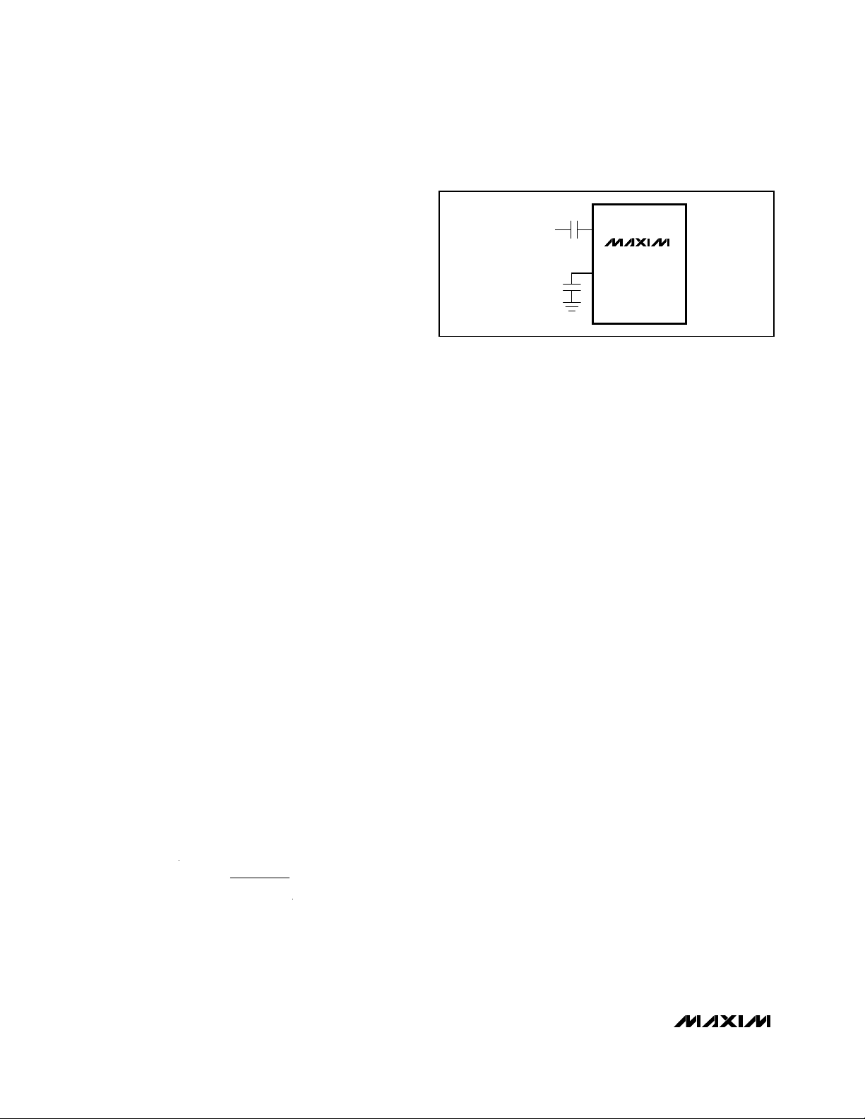
Single-Ended Input
The MAX9700 can be configured as a single-ended
input amplifier by capacitively coupling either input to
GND and driving the other input (Figure 6).
DC-Coupled Input
The input amplifier can accept DC-coupled inputs that
are biased within the amplifier’s common-mode range
(see the Typical Operating Characteristics). DC coupling eliminates the input-coupling capacitors, reducing component count to potentially one external
component (see the System Diagram). However, the
low-frequency rejection of the capacitors is lost, allowing low-frequency signals to feedthrough to the load.
Component Selection
Input Filter
An input capacitor, CIN, in conjunction with the input
impedance of the MAX9700 forms a highpass filter that
removes the DC bias from an incoming signal. The ACcoupling capacitor allows the amplifier to bias the signal to an optimum DC level. Assuming zero source
impedance, the -3dB point of the highpass filter is
given by:
Choose CINso f
-3dB
is well below the lowest frequency
of interest. Setting f
-3dB
too high affects the low-fre-
quency response of the amplifier. Use capacitors
whose dielectrics have low-voltage coefficients, such
as tantalum or aluminum electrolytic. Capacitors with
high-voltage coefficients, such as ceramics, may result
in increased distortion at low frequencies.
Other considerations when designing the input filter
include the constraints of the overall system and the
actual frequency band of interest. Although high-fidelity
audio calls for a flat gain response between 20Hz and
20kHz, portable voice-reproduction devices such as
cellular phones and two-way radios need only concentrate on the frequency range of the spoken human
voice (typically 300Hz to 3.5kHz). In addition, speakers
used in portable devices typically have a poor response
below 150Hz. Taking these two factors into consideration, the input filter may not need to be designed for a
20Hz to 20kHz response, saving both board space and
cost due to the use of smaller capacitors.
Output Filter
The MAX9700 does not require an output filter. The
device passes FCC emissions standards with 100mm
of unshielded speaker cables. However, output filtering
can be used if a design is failing radiated emissions
due to board layout or cable length, or the circuit is
near EMI-sensitive devices. Use an LC filter when radiated emissions are a concern, or when long leads are
used to connect the amplifier to the speaker.
Supply Bypassing/Layout
Proper power-supply bypassing ensures low-distortion
operation. For optimum performance, bypass V
DD
to
GND and PVDDto PGND with separate 0.1µF capacitors as close to each pin as possible. A low-impedance, high-current power-supply connection to PVDDis
assumed. Additional bulk capacitance should be
added as required depending on the application and
power-supply characteristics. GND and PGND should
be star connected to system ground. Refer to the
MAX9700 evaluation kit for layout guidance.
f
RC
dB
IN IN
−=3
1
2π
Figure 6. Single-Ended Input
1µF
1µF
IN+
MAX9700
IN-
SINGLE-ENDED
AUDIO INPUT
Page 13

MAX9700
1.2W, Low-EMI, Filterless,
Class D Audio Amplifier
______________________________________________________________________________________ 13
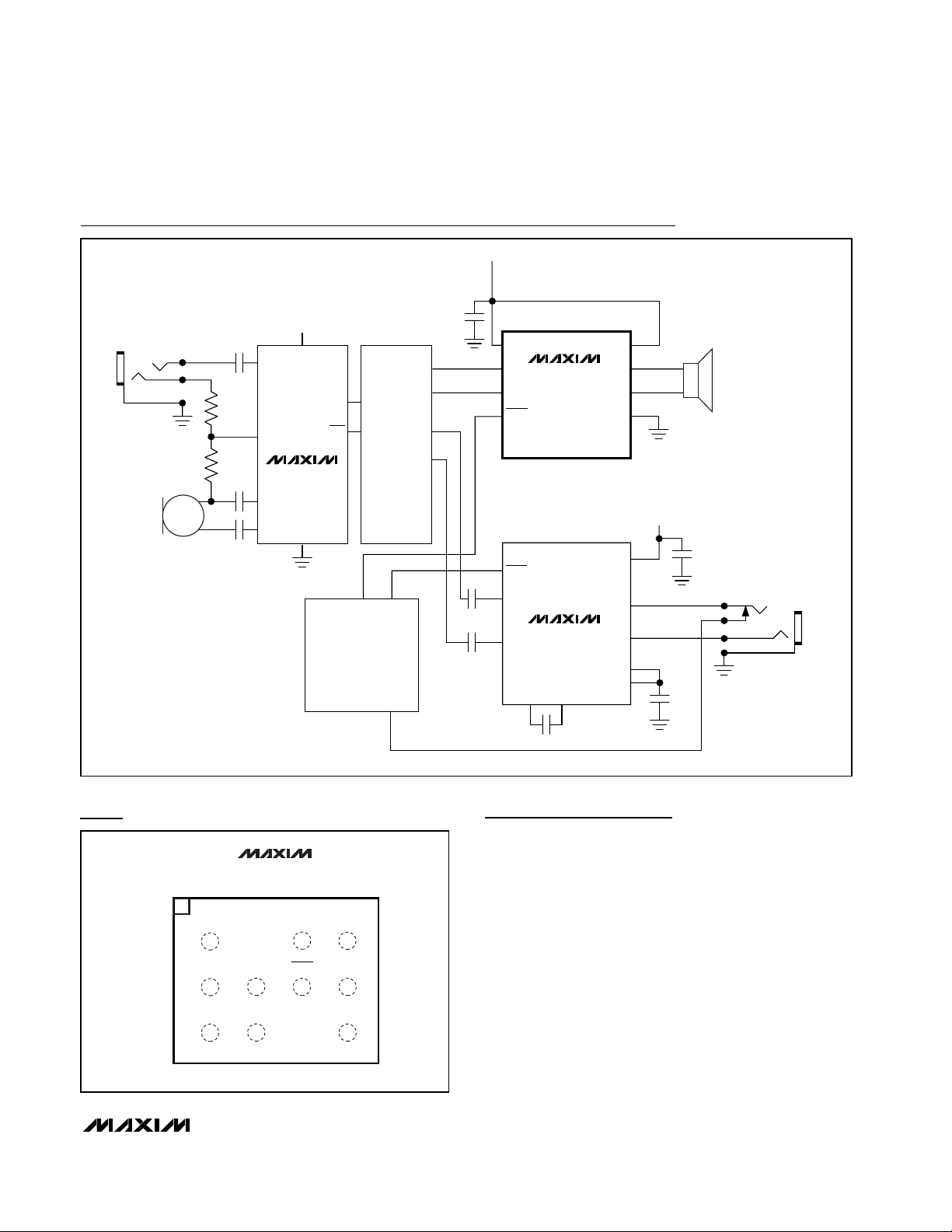
Stereo Configuration
Two MAX9700s can be configured as a stereo amplifier
(Figure 7). Device U1 is the master amplifier; its unfiltered output drives the SYNC input of the slave device
(U2), synchronizing the switching frequencies of the two
devices. Synchronizing two MAX9700s ensures that no
beat frequencies occur within the audio spectrum. This
configuration works when the master device is in either
FFM or SSM mode. There is excellent THD+N performance and minimal crosstalk between devices due to
the SYNC connection (Figures 8 and 9). U2 locks onto
only the frequency present at SYNC, not the pulse
width. The internal feedback loop of device U2 ensures
that the audio component of U1’s output is rejected.
Designing with Volume Control
The MAX9700 can easily be driven by single-ended
sources (Figure 6), but extra care is needed if the
source impedance “seen” by each differential input is
unbalanced, such as the case in Figure 10a, where the
MAX9700 is used with an audio taper potentiometer
acting as a volume control. Functionally, this configuration works well, but can suffer from click-pop transients
at power-up (or coming out of SHDN) depending on the
volume-control setting. As shown, the click-pop performance is fine for either max or min volume, but worsens
at other settings.
Figure 7. Master-Slave Stereo Configuration
Figure 8. Master-Slave THD+N
Figure 9. Master-Slave Crosstalk
1µF
RIGHT-CHANNEL
DIFFERENTIAL
AUDIO INPUT
1µF
LEFT-CHANNEL
DIFFERENTIAL
AUDIO INPUT
V
DD
V
IN+
IN-
DD
MAX9700
PV
OUT+
OUT-
SYNC
DD
V
IN+
DD
MAX9700
PV
OUT+
DD
IN-
OUT-
SYNC
TOTAL HARMONIC DISTORTION PLUS NOISE
vs. OUTPUT POWER
100
VDD = 3.3V
f = 1kHz
= 8Ω
R
10
L
SLAVE DEVICE
1
THD+N (%)
0.1
0.01
0.001
0 0.1 0.2 0.3 0.4 0.5
OUTPUT POWER (W)
CROSSTALK vs. FREQUENCY
0
VDD = 3.3V
= 8Ω
R
L
-20
f = 1kHz
= 500mV
V
IN
-40
-60
CROSSTALK (dB)
-80
-100
-120
10 100 1k 10k 100k
P-P
MASTER-TO-SLAVE
SLAVE-TO-MASTER
FREQUENCY (Hz)
Page 14

MAX9700
One solution is the configuration shown in Figure 10b.
The potentiometer is connected between the differential
inputs, and these “see” identical RC paths when the
device powers up. The variable resistive element
appears between the two inputs, meaning the setting
affects both inputs the same way. The potentiometer is
audio taper, as in Figure 10a. This significantly
improves transient performance on power-up or release
from SHDN. A similar approach can be applied when
the MAX9700 is driven differentially and a volume control is required.
UCSP Applications Information
For the latest application details on UCSP construction,
dimensions, tape carrier information, PC board techniques, bump-pad layout, and recommended reflow temperature profile, as well as the latest information on
reliability testing results, refer to the Application Note:
UCSP—A Wafer-Level Chip-Scale Package available on
Maxim’s website at www.maxim-ic.com/ucsp.
1.2W, Low-EMI, Filterless,
Class D Audio Amplifier
14 ______________________________________________________________________________________
Figure 10a. Single-Ended Drive of MAX9700 Plus Volume
Figure 10b. Improved Single-Ended Drive of MAX9700 Plus
Volume
Ordering Information (continued)
Selector Guide
*Future Product—contact factory for availability.
CW
50kΩ
1µF
IN-
MAX9700
IN+
1µF
1µF
22kΩ
CW
50kΩ
1µF
22kΩ
IN-
MAX9700
IN+
PART TEMP RANGE
o
MAX9700CETB* -40
MAX9700CEUB* -40oC to +85oC 10 µMAX —
MAX9700CEBC-T* -40oC to +85oC 12 UCSP-12 —
MAX9700DETB* -40oC to +85oC 10 TDFN ACO
MAX9700DEUB* -40oC to +85oC 10 µMAX —
MAX9700DEBC-T* -40oC to +85oC 12 UCSP-12 —
C to +85oC 10 TDFN ACN
PINPACKAGE
TOP
MARK
MAX9700AETB 10 TDFN 6
MAX9700AEUB 10 µMAX 6
MAX9700AEBC-T 12 UCSP-12 6
MAX9700BETB 10 TDFN 12
MAX9700BEUB 10 µMAX 12
MAX9700BEBC-T 12 UCSP-12 12
MAX9700CETB 10 TDFN 15.6
MAX9700CEUB 10 µMAX 15.6
MAX9700CEBC-T 12 UCSP-12 15.6
MAX9700DETB 10 TDFN 20
MAX9700DEUB 10 µMAX 20
MAX9700DEBC-T 12 UCSP-12 20
PART PIN-PACKAGE GAIN (dB)
Page 15
MAX9700
1.2W, Low-EMI, Filterless,
Class D Audio Amplifier
______________________________________________________________________________________ 15
Chip Information
TRANSISTOR COUNT: 3595
PROCESS: BiCMOS
System Diagram
MAX9700
TOP VIEW
(BUMP SIDE DOWN)
UCSP
GND
IN-
OUT-
1
A
B
C
234
OUT+ V
DD
SYNC
PV
DD
SHDN IN+
PGND
Pin Configurations (continued)
0.1µF
2.2kΩ
2.2kΩ
0.1µF
0.1µF
V
DD
V
DD
AUX_IN
BIAS
MAX4063
IN+
IN-
OUT
OUT
PROCESSOR
µCONTROLLER
CODEC/
BASEBAND
1µF
1µF
1µF
V
DD
IN+
IN-
SHDN
SHDN
INL
INR
C1P CIN
MAX9700
MAX9722
PV
OUT+
OUT-
SYNC
V
OUTL
OUTR
PV
SV
DD
DD
SS
SS
V
DD
1µF
1µF
1µF
Page 16

MAX9700
1.2W, Low-EMI, Filterless,
Class D Audio Amplifier
16 ______________________________________________________________________________________
Package Information
(The package drawing(s) in this data sheet may not reflect the most current specifications. For the latest package outline information
go to www.maxim-ic.com/packages
.)
PACKAGE OUTLINE, 4x3 UCSP
21-0104
12L, UCSP 4x3.EPS
1
F
1
Page 17

MAX9700
1.2W, Low-EMI, Filterless,
Class D Audio Amplifier
______________________________________________________________________________________ 17
Package Information (continued)
(The package drawing(s) in this data sheet may not reflect the most current specifications. For the latest package outline information
go to www.maxim-ic.com/packages
.)
D
PIN 1
INDEX
AREA
A
A2
b
E
A1
L
DETAIL A
E2
e
C
L
C0.35
D2
C
L
L
PIN 1 ID
1N1
[(N/2)-1] x e
REF.
k
L
6, 8, &10L, DFN THIN.EPS
A
NUMBER OF LEADS SHOWN ARE FOR REFERENCE ONLY
e
PROPRIETARY INFORMATION
TITLE:
PACKAGE OUTLINE, 6, 8 & 10L,
TDFN, EXPOSED PAD, 3x3x0.80 mm
APPROVAL
e
DALLAS
SEMICONDUCTOR
DOCUMENT CONTROL NO. REV.
21-0137 D
1
2
Page 18

MAX9700
1.2W, Low-EMI, Filterless,
Class D Audio Amplifier
18 ______________________________________________________________________________________
Package Information (continued)
(The package drawing(s) in this data sheet may not reflect the most current specifications. For the latest package outline information
go to www.maxim-ic.com/packages
.)
COMMON DIMENSIONS
SYMBOL
A
D
E
A1
L
k
A2 0.20 REF.
PACKAGE VARIATIONS
PKG. CODE
T633-1 1.50±0.10D22.30±0.10
MIN. MAX.
0.70 0.80
2.90 3.10
2.90 3.10
0.00 0.05
0.20 0.40
N
6
0.25 MIN.
1.50±0.10
E2
0.95 BSCeMO229 / WEEA
2.30±0.10T833-1 8
0.65 BSC
JEDEC SPEC
MO229 / WEEC
[(N/2)-1] x e
0.40±0.05b1.90 REF
1.95 REF0.30±0.05
0.25±0.05 2.00 REFMO229 / WEED-30.50 BSC1.50±0.10 2.30±0.1010T1033-1
DALLAS
SEMICONDUCTOR
PROPRIETARY INFORMATION
TITLE:
PACKAGE OUTLINE, 6, 8 & 10L,
TDFN, EXPOSED PAD, 3x3x0.80 mm
DOCUMENT CONTROL NO.APPROVAL
21-0137
REV.
2
2
D
Page 19

MAX9700
1.2W, Low-EMI, Filterless,
Class D Audio Amplifier
Maxim cannot assume responsibility for use of any circuitry other than circuitry entirely embodied in a Maxim product. No circuit patent licenses are
implied. Maxim reserves the right to change the circuitry and specifications without notice at any time.
Maxim Integrated Products, 120 San Gabriel Drive, Sunnyvale, CA 94086 408-737-7600 ____________________ 19
© 2003 Maxim Integrated Products Printed USA is a registered trademark of Maxim Integrated Products.
Package Information (continued)
(The package drawing(s) in this data sheet may not reflect the most current specifications. For the latest package outline information
go to www.maxim-ic.com/packages
.)
e
10
ÿ 0.50±0.1
0.6±0.1
1
0.6±0.1
TOP VIEW
D2
A2
D1
FRONT VIEW
4X S
10
H
1
BOTTOM VIEW
E2
GAGE PLANE
A
b
A1
α
E1
L
L1
SIDE VIEW
INCHES
MIN
DIM
-A
A1
0.002
A2 0.030 0.037 0.75 0.95
D1
0.116
0.114
D2
0.116
E1
0.114
E2
0.187
H
0.0157
L
L1
0.037 REF
0.007
b
e
0.0197 BSC
0.0035
c
0.0196 REF
S
α
0∞ 0∞ 6∞
c
MAX
0.043
0.006
0.120
0.118
0.120
0.118
0.199
0.0275
0.0106
0.0078
6∞
MILLIMETERS
MAX
MIN
1.10
-
0.15
0.05
3.05
2.95
2.89
3.00
3.05
2.95
2.89
3.00
4.75
5.05
0.40
0.70
0.940 REF
0.177
0.270
0.500 BSC
0.090
0.200
0.498 REF
10LUMAX.EPS
PROPRIETARY INFORMATION
TITLE:
PACKAGE OUTLINE, 10L uMAX/uSOP
REV.DOCUMENT CONTROL NO.APPROVAL
21-0061
1
I
1
 Loading...