

Page 1
_______________General Description
The MAX965–MAX970 single/dual/quad micropower
comparators feature Rail-to-Rail®inputs and outputs, and
fully specified single-supply operation down to +1.6V.
These devices draw less than 5µA per comparator and
have open-drain outputs that can be pulled beyond V
CC
to 6V (max) above ground. In addition, their rail-to-rail
input common-mode voltage range makes these comparators suitable for ultra-low-voltage operation.
A +1.6V to +5.5V single-supply operating voltage range
makes the MAX965 family of comparators ideal for 2-cell
battery-powered applications. The MAX965/MAX967/
MAX968/MAX969 offer programmable hysteresis and
an internal 1.235V ±1.5% reference. All devices are
available in either space-saving 8-pin µMAX or 16-pin
QSOP packages.
________________________Applications
2-Cell Battery-Powered/Portable Systems
Window Comparators
Threshold Detectors/Discriminators
Mobile Communications
Voltage-Level Translation
Ground/Supply-Sensing Applications
____________________________Features
♦ Ultra-Low Single-Supply Operation down to +1.6V
♦ Rail-to-Rail Common-Mode Input Voltage Range
♦ 3µA Quiescent Supply Current per Comparator
♦ Open-Drain Outputs Swing Beyond V
CC
♦ 1.235V ±1.5% Precision Internal Reference
(MAX965/967/968/969)
♦ 10µs Propagation Delay (50mV overdrive)
♦ Available in Space-Saving Packages:
8-Pin µMAX (MAX965–MAX968)
16-Pin QSOP (MAX969/MAX970)
MAX965–MAX970
Single/Dual/Quad, Micropower,
Ultra-Low-V oltage, Rail-to-Rail I/O Comparators
________________________________________________________________
Maxim Integrated Products
1
V
CC
V
OUT
7
OUT
GND
1.235V
REF6
HYST
1
5
IN-4
IN+3
8
V
CC
V
IN
R
PULL-UP
MAX965
__________Typical Operating Circuit
19-1226; Rev 0; 4/97
PART
MAX965ESA
MAX965EUA
MAX966ESA
-40°C to +85°C
-40°C to +85°C
-40°C to +85°C
TEMP. RANGE PIN-PACKAGE
8 SO
8 µMAX
8 SO
______________Ordering Information
Rail-to-Rail is a registered trademark of Nippon Motorola Ltd.
For free samples & the latest literature: http://www.maxim-ic.com, or phone 1-800-998-8800
MAX966EUA -40°C to +85°C 8 µMAX
MAX967ESA
-40°C to +85°C 8 SO
MAX967EUA -40°C to +85°C 8 µMAX
PART
INTERNAL
REFERENCE
PROGRAMMABLE
HYSTERESIS
MAX965
Yes Yes
MAX966
No No
MAX967
Yes Yes
MAX968
Yes Yes
MAX969
Yes Yes
MAX970
No No
COMPARATORS
PER
PACKAGE
1
2
2
2
4
4
_____________________Selector Guide
Ordering Information continued on last page.
Pin Configurations appear at end of data sheet.
Page 2
MAX965–MAX970
Single/Dual/Quad, Micropower,
Ultra-Low-V oltage, Rail-to-Rail I/O Comparators
ABSOLUTE MAXIMUM RATINGS
ELECTRICAL CHARACTERISTICS
(VCC= +1.6V to +5.5V, TA= T
MIN
to T
MAX
, unless otherwise noted. Typical values are at VCC= 3V and TA= +25°C.)
Stresses beyond those listed under “Absolute Maximum Ratings” may cause permanent damage to the device. These are stress ratings only, and functional
operation of the device at these or any other conditions beyond those indicated in the operational sections of the specifications is not implied. Exposure to
absolute maximum rating conditions for extended periods may affect device reliability.
Supply Voltage (VCC) ............................................................+6V
Voltages
IN_-, IN_+, REF, HYST ..........................-0.3V to (V
CC
+ 0.3V)
OUT_ ...............................................................-0.3V to +6.0V
Duration of OUT_ Short Circuit to GND or V
CC
..........Continuous
Continuous Power Dissipation
8-Pin SO (derate 5.88mW/°C above +70°C)...............471mW
8-Pin µMAX (derate 4.10mW/°C above +70°C)..........330mW
14-Pin SO (derate 8.33mW/°C above +70°C).............667mW
16-Pin SO (derate 8.70mW/°C above +70°C).............696mW
16-Pin QSOP (derate 5.70mW/°C above +70°C)........457mW
Operating Temperature Range ...........................-40°C to +85°C
Storage Temperature Range.............................-65°C to +150°C
Lead Temperature (soldering, 10sec).............................+300°C
6.0
10.00°C to +85°C
µMAX
package
QSOP package
-40°C to +85°C
Input Offset Voltage V
OS
-40°C to +85°C
0°C to +85°C
QSOP package
SO package 3.0
Common-mode
range = -0.25V
to 1.3V,
VCC> 1.8V
mV
V
-0.25 V
CC
- 0.25
TA= -40°C to +85°C
SO/QSOP packages, TA= -40°C to +85°C
Full common-mode range, TA= +25°C
Common-mode range = -0.25V to (VCC- 0.25V)
All packages, TA= 0°C to +85°C
VCCstepped 0V to 5V
MAX970
MAX966
MAX967/MAX968
TA= +25°C
MAX969
1.7V ≤ VCC≤ 5.5V
CONDITIONS
7.0C
IN
Input Capacitance pF
0.2I
OS
Input Offset Current
0.001 ±50
nA
0.001 ±5
I
B
Input Bias Current
4.0
-0.25 V
CC
V
CMR
Common-Mode Voltage Range
V
0.1 1.0
PSRRPower-Supply Rejection Ratio
1.7 5.5V
CC
Supply Voltage Range V
1.6 5.5
mV/V
20
Power-Up Time
(VCCto output valid)
11 18
µA
7.0 12
I
CC
Supply Current
6.0 10
10 16
14 22
UNITSMIN TYP MAXSYMBOLPARAMETER
4.0
15.0
10.0
Full commonmode range
7.0
µMAX package, TA= -40°C to +85°C 1.8 5.5
MAX965
Comparator Minimum
Operating Voltage
V1.0
µs
pA
HYST = REF mV±1V
HYST
Input Hysteresis
2 _______________________________________________________________________________________
COMPARATOR
POWER SUPPLIES
SO package
µMAX
package
Page 3
V
MAX965–MAX970
Single/Dual/Quad, Micropower,
Ultra-Low-V oltage, Rail-to-Rail I/O Comparators
_______________________________________________________________________________________
3
3
4
-60
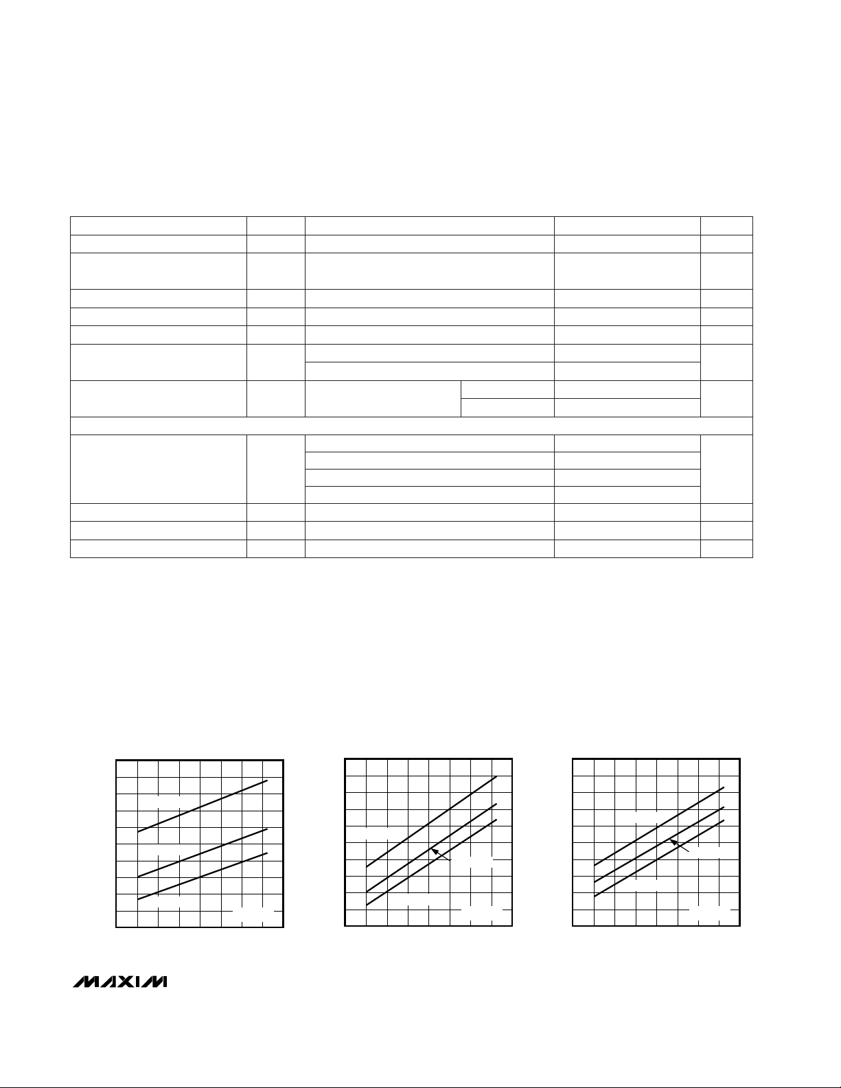
MAX965 SUPPLY CURRENT
vs. TEMPERATURE
MAX965-TOC1b
TEMPERATURE (°C)
SUPPLY CURRENT (µA)
5
7
6
8
9
10
11
12
13
-40 -20 0 20 40 60 80 100
V
IN+
> V
IN-
VCC = 5.0V
VCC = 2.0V
VCC = 3.0V
4.0
-60
MAX966 SUPPLY CURRENT
vs. TEMPERATURE
MAX965-TOC2b
TEMPERATURE (°C)
SUPPLY CURRENT (µA)
4.5
5.5
5.0
6.0
6.5
7.0
7.5
8.0
8.5
9.0
-40 -20 0 20 40 60 80 100
V
IN+
> V
IN-
VCC = 5.0V
VCC = 2.0V
VCC = 3.0V
5
-60
MAX967/MAX968 SUPPLY CURRENT
vs. TEMPERATURE
MAX965-TOC3b
TEMPERATURE (°C)
SUPPLY CURRENT (µA)
6
8
7
9
10
11
12
13
14
15
-40 -20 0 20 40 60 80 100
V
IN+
> V
IN-
VCC = 5.0V
VCC = 2.0V
VCC = 3.0V
ELECTRICAL CHARACTERISTICS (continued)
(VCC= +1.6V to +5.5V, TA= T
MIN
to T
MAX
, unless otherwise noted. Typical values are at VCC= 3V and TA= +25°C.)
f = 100Hz to 100kHz, C
REF
= 0.1µF
HYST = REF
SO package
CONDITIONS
µV
RMS
10Output Voltage Noise
nA200 400I
REF-
Sink Current
µA15 50I
REF+
Source Current
V
1.125 1.235 1.255
V
REF
Reference Voltage
UNITSMIN TYP MAXSYMBOLPARAMETER
1.205 1.235 1.265
__________________________________________Typical Operating Characteristics
(VCC= +3.0V, R
PULL-UP
= 100kΩ, VCM= 0V, TA= +25°C, unless otherwise noted.)
10
CMRRCommon-Mode Rejection Ratio mV/V1.5 4.0
f = 100Hz to 100kHz, C
REF
= 1000pFInput Voltage Noise e
n
µV
RMS
0.2I
OUT
= 100µA, 1.6V < VCC< 2.7V
OUT Output Voltage Low V
OL
V
20
Propagation Delay t
PD-
µs
10
R
PULL-UP
= 1MΩ,
C
LOAD
= 15pF, high to low
10mV overdrive
50mV overdrive
QSOP package
HYST Input Voltage Range V
V
REF -
0.05
V
REF
I
HYST
HYST Input Leakage nA±5
Hysteresis Gain V/V1.0
µMAX package, TA= -40°C to +85°C 1.185 1.235 1.285
µMAX package, TA= 0°C to +85°C 1.205 1.235 1.265
0.4I
OUT
= 500µA, 2.7V < VCC< 5.5V
REFERENCE
Page 4
MAX965–MAX970
Single/Dual/Quad, Micropower,
Ultra-Low-V oltage, Rail-to-Rail I/O Comparators
4 _______________________________________________________________________________________
0
0
MAX965 SUPPLY CURRENT
vs. SUPPLY VOLTAGE
(INCLUDES REFERENCE CURRENT)
MAX965/70-TOC7a
SUPPLY VOLTAGE (V)
SUPPLY CURRENT (µA)
2
4
6
8
10
12
14
1 2 3 4 5 6
V
IN+
> V
IN-
-60 -20 0-40 20 40 60 80 100
COMPARATOR OUTPUT SHORT-CIRCUIT
SINK CURRENT vs. TEMPERATURE
MAX965/70 -TOC8a
TEMPERATURE (°C)
OUTPUT SHORT-CIRCUIT SINK CURRENT (mA)
VCC = 2V
VCC = 3V
V
IN+
< V
IN-
VCC = 5V
0
2
4
6
8
10
12
14
0
1.5
1.0
0.5
2.0
2.5
3.0
3.5
4.0
4.5
5.0
0 42 6 8 10 12
COMPARATOR OUTPUT
LOW VOLTAGE vs. SINK CURRENT
MAX965/70-09a
SINK CURRENT (mA)
OUTPUT LOW VOLTAGE (V)
V
IN+
= < V
IN-
V
CC
= 5V
V
CC
= 3V
V
CC
= 2V
6
-60
PROPAGATION DELAY (t
PD-
)
vs. TEMPERATURE
MAX965-TOC10a
TEMPERATURE (°C)
DELAY (µs)
7
4
5
9
8
10
11
12
13
14
-40 -20 0 20 40 60 80 100
VOD = 50mV
VCC = 2.0V
VCC = 5.0V
VCC = 3.0V
70
0
0.001 0.01 0.1
PROPAGATION DELAY (t
PD-
)
vs. CAPACITIVE LOAD
10
MAX4108/9-11a
CAPACITIVE LOAD (µF)
DELAY (µs)
30
20
40
50
60
VOD = 50mV
VCC = 5.0V
VCC = 3.0V
VCC = 2.0V
0
0
PROPAGATION DELAY (t
PD-
)
vs. INPUT OVERDRIVE
MAX965-TOC12a
INPUT OVERDRIVE (mV)
DELAY (µs)
10
5
15
20
25
30
20 40 60 80 100 120 140 160
VCC = 5.0V
VCC = 2.0V
VCC = 3.0V
_____________________________Typical Operating Characteristics (continued)
(VCC= +3.0V, R
PULL-UP
= 100kΩ, VCM= 0V, TA= +25°C, unless otherwise noted.)
8
-60
MAX969 SUPPLY CURRENT
vs. TEMPERATURE
MAX965-TOC4b
TEMPERATURE (°C)
SUPPLY CURRENT (µA)
12
10
14
16
18
20
-40 -20 0 20 40 60 80 100
V
IN+
> V
IN-
VCC = 5.0V
VCC = 2.0V
VCC = 3.0V
7
-60
MAX970 SUPPLY CURRENT
vs. TEMPERATURE
MAX965-TOC5b
TEMPERATURE (°C)
SUPPLY CURRENT (µA)
8
10
9
11
12
13
14
15
16
-40 -20 0 20 40 60 80 100
V
IN+
> V
IN-
VCC = 2.0V
VCC = 3.0V
VCC = 5.0V
0
0
SUPPLY CURRENT PER COMPARATOR
vs. SUPPLY VOLTAGE
(EXCLUDES REFERENCE CURRENT)
MAX965-TOC6b
SUPPLY VOLTAGE (V)
SUPPLY CURRENT PER COMPARATOR (µA)
0.5
1.0
1.5
2.0
2.5
3.0
3.5
1 2 3 4 5 6
V
IN+
> V
IN-
Page 5

MAX965–MAX970
Single/Dual/Quad, Micropower,
Ultra-Low-V oltage, Rail-to-Rail I/O Comparators
_______________________________________________________________________________________ 5
4.0
3.8
2.0
0.01 0.1 1 10 100
SUPPLY CURRENT PER COMPARATOR
vs. OUTPUT TRANSITION FREQUENCY
2.4
2.2
MAX965/70 TOC13A
OUTPUT TRANSITION FREQUENCY (kHz)
SUPPLY CURRENT PER COMPARATOR (µA)
2.8
2.6
3.2
3.0
3.6
3.4
VCC = 5.5V
VCC = 1.6V
100
120
110
140
130
160
150
170
190
180
200
-60 -20 0-40 20 40 60 80 100
INPUT OFFSET VOLTAGE
vs. TEMPERATURE
MAX965/70-TOC14a
TEMPERATURE (°C)
INPUT OFFSET VOLTAGE (µV)
0
1.0
0.5
2.0
1.5
3.5
3.0
2.5
4.0
-40 -20 0 20 40 60 80 100
INPUT BIAS CURRENT
vs. TEMPERATURE
MAX965/70-TOC15a
TEMPERATURE (°C)
INPUT BIAS CURRENT (pA)
VCC = 5.0V
VCC = 3.0V
0
10
5
15
30
35
25
20
40
0 1.0 1.5 2.0 2.50.5 3.0 3.5 4.0 4.5 5.0
PROGRAMMED HYSTERESIS
vs. COMMON-MODE VOLTAGE
MAX965/70 TOC16
COMMON-MODE VOLTAGE (V)
PROGRAMMED HYSTERESIS (mV)
V
CC
= 5.0V
V
HYST
= 22mV (PROGRAMMED)
1.2320
1.2325
1.2335
1.2330
1.2340
1.2345
-60 -20 0-40 20 40 60 80 100
REFERENCE VOLTAGE
vs. TEMPERATURE
MAX965/70 TOC6a
TEMPERATURE (°C)
REFERENCE VOLTAGE (V)
VCC = 5V
VCC = 3V
VCC = 2V
1.223
1.229
1.227
1.225
1.231
1.233
1.237
1.235
1.239
1.0 1.8 2.6 3.4 4.2 5.0 5.8
REFERENCE VOLTAGE
vs. SUPPLY VOLTAGE
MAX965/70-TOC13
V
CC
(V)
REFERENCE VOLTAGE (V)
0.6
0.8
0.7
1.0
0.9
1.3
1.2
1.1
1.4
0 200100 300 400 500 600 700
REFERENCE VOLTAGE
vs. SOURCE CURRENT
MAX965/70-TOC18a
SOURCE CURRENT (µA)
REFERENCE VOLTAGE (V)
_____________________________Typical Operating Characteristics (continued)
(VCC= +3.0V, R
PULL-UP
= 100kΩ, VCM= 0V, TA= +25°C, unless otherwise noted.)
IN+
OUT
PROPAGATION DELAY (t
PD+
)
MAX965/70-TOC15
2µs/div
VCC = 3V
50mV/div
2V/div
50mV/div
2V/div
IN+
OUT
PROPAGATION DELAY (t
PD-
)
MAX965/70-TOC16b
2µs/div
VCC = 3V
Page 6

MAX965–MAX970
Single/Dual/Quad, Micropower,
Ultra-Low-V oltage, Rail-to-Rail I/O Comparators
6 _______________________________________________________________________________________
_____________________________________________________________Pin Descriptions
FUNCTION
PIN
MAX965
MAX966
— 1 Comparator A Open-Drain Output
1 2 Ground
2 — No Connection. Not internally connected.
— 4 Comparator A Inverting Input
4 — Comparator Inverting Input
— 3 Comparator A Noninverting Input
3 — Comparator Noninverting Input
7 7 Positive Supply Voltage, +1.6V to +5.5V
6 — Internal Reference Output. Typically 1.235V with respect to GND.
5 —
Hysteresis Input. Connect HYST to REF if not used. Input voltage range
is from V
REF
to (V
REF
- 50mV).
— 6 Comparator B Noninverting Input
— 5 Comparator B Inverting Input
MAX967
1
2
—
—
—
3
—
7
6
5
4
—
MAX968
1
2
—
—
—
3
—
7
6
5
—
4
NAME
OUTA
GND
N.C.
INA-
IN-
INA+
IN+
V
CC
REF
HYST
INB+
INB-
8 — — — OUT Comparator Open-Drain Output
— 8 8 8 OUTB Comparator B Open-Drain Output
MAX965–MAX968
50mV/div
1V/div
IN+
OUT
10kHz RESPONSE
MAX965/70-TOC18
20µs/div
2V/div
2V/div
V
CC
OUT
POWER-UP/DOWN RESPONSE
MAX965/70-TOC17
5µs/div
_____________________________Typical Operating Characteristics (continued)
(VCC= +3.0V, R
PULL-UP
= 100kΩ, V
CM
= 0V, TA= +25°C, unless otherwise noted.)
Page 7

MAX965–MAX970
Single/Dual/Quad, Micropower,
Ultra-Low-V oltage, Rail-to-Rail I/O Comparators
_______________________________________________________________________________________ 7
________________________________________________Pin Descriptions (continued)
_______________Detailed Description
The MAX965–MAX970 single/dual/quad, micropower,
ultra-low-voltage comparators feature Rail-to-Rail
®
inputs and outputs and an internal 1.235V ±1.5%
bandgap reference. These devices operate from a single +1.6V to +5.5V supply voltage range, and consume
less than 5µA supply current per comparator over the
extended temperature range. Internal hysteresis is programmable up to ±50mV using two external resistors
and the device’s internal reference. The rail-to-rail input
common-mode voltage range and the open-drain outputs allow easy voltage-level conversion for multivoltage systems. All inputs and outputs can tolerate a
continuous short-circuit fault condition to either rail.
The MAX965 is a single comparator with adjustable
hysteresis and a reference output pin. The MAX966 is a
dual comparator without the reference and without
adjustable hysteresis. The MAX967 is a dual compara-
tor configured as a dual voltage monitor with common
hysteresis adjustment and a reference output. The dual
MAX968 is similar to the MAX967, but is configured as
a window comparator. The MAX969 is a quad comparator with a common hysteresis adjustment and a reference output pin. The MAX970 is a quad comparator
without a reference and without hysteresis adjustment.
(See Functional Diagrams and Selector Guide.)
Comparator Input
The MAX965–MAX970 have a -0.25V to VCCinput common-mode range. Both comparator inputs may operate
at any differential voltage within the common-mode
voltage range, and the comparator displays the correct
output logic state.
Low-Voltage Operation: VCCDown to 1V
The minimum operating voltage is 1.6V. As the supply
voltage falls below 1.6V, performance degrades
and supply current falls. The reference does not
MAX969/MAX970
FUNCTION
MAX969
SO
4 4 Comparator A Inverting Input
3 3 Positive Supply Voltage, +1.6V to +5.5V
2 2 Comparator A Open-Drain Output
1 1 Comparator B Open-Drain Output
8 — Internal Reference Output. Typically 1.235V with respect to GND.
— — No Connection. Not internally connected.
7 7 Comparator B Noninverting Input
6 6 Comparator B Inverting Input
5 5 Comparator A Noninverting Input
MAX970
QSOP
4
3
2
1
—
8, 9
7
6
5
NAME
INA-
VCC
OUTA
OUTB
REF
N.C.
INB+
INB-
INA+
PIN
9 — — HYST
Hysteresis Input. Connect to REF if not used. Input voltage range is
from (V
REF
- 50mV) to V
REF
.
10 8 10 INC- Comparator C Inverting Input
11 9 11 INC+ Comparator C Noninverting Input
12 10 12 IND- Comparator D Inverting Input
13 11 13 IND+ Comparator D Noninverting Input
14 12 14 GND Ground
15 13 15 OUTD Comparator D Open-Drain Output
16 14 16 OUTC Comparator C Open-Drain Output
Page 8

MAX965–MAX970
Single/Dual/Quad, Micropower,
Ultra-Low-V oltage, Rail-to-Rail I/O Comparators
8 _______________________________________________________________________________________
OUTB
OUTA
INAINA+
INBINB+
REF
OUTC
V
CC
V
CC
OUTD
IND+
IND-
INC+
INC-
+
1.235V
GND HYST
OUTB
OUTA
INAINA+
INBINB+
OUTC
OUTD
IND+
IND-
INC+
INC-
GND
MAX969 MAX970
V
CC
V
CC
OUT
IN+ OUTA
INA+
GND
GND
GND
INA-
INB+
INB-
OUTB
OUTA
INA+
REF
REF
REF
REF
REF
V
CC
V
CC
1.235V
1.235V
INB-
HYST
OUTB
OUTA
INA+
REF
INB+
HYST
OUTB
IN-
HYST
REF
+
GND
1.235V
MAX965
MAX968MAX967
MAX966
________________________________________________________Functional Diagrams
Page 9

MAX965–MAX970
Single/Dual/Quad, Micropower,
Ultra-Low-V oltage, Rail-to-Rail I/O Comparators
function below about 1.5V, although the comparators
typically continue to operate with a supply voltage as
low as 1V. At low supply voltages (<1.6V), the input
common-mode range remains rail-to-rail, but the comparator’s output sink capability is reduced and propagation delay increases (see Typical Operating
Characteristics).
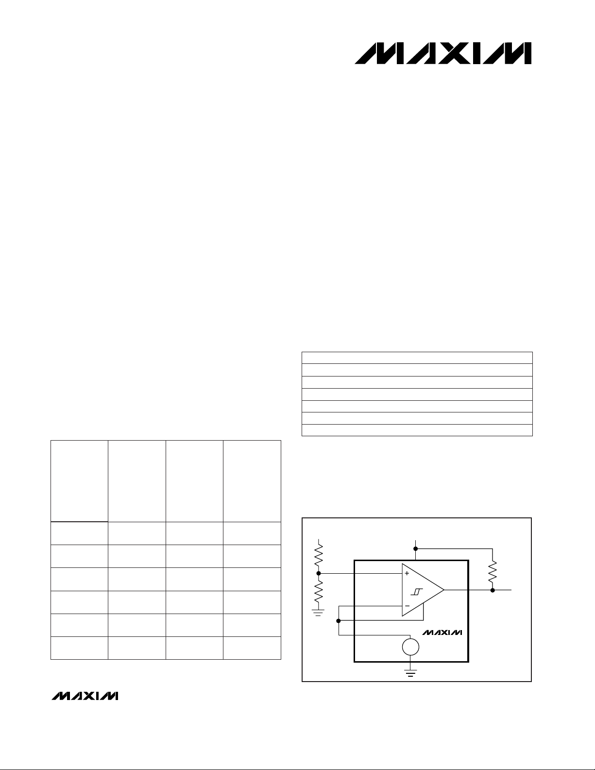
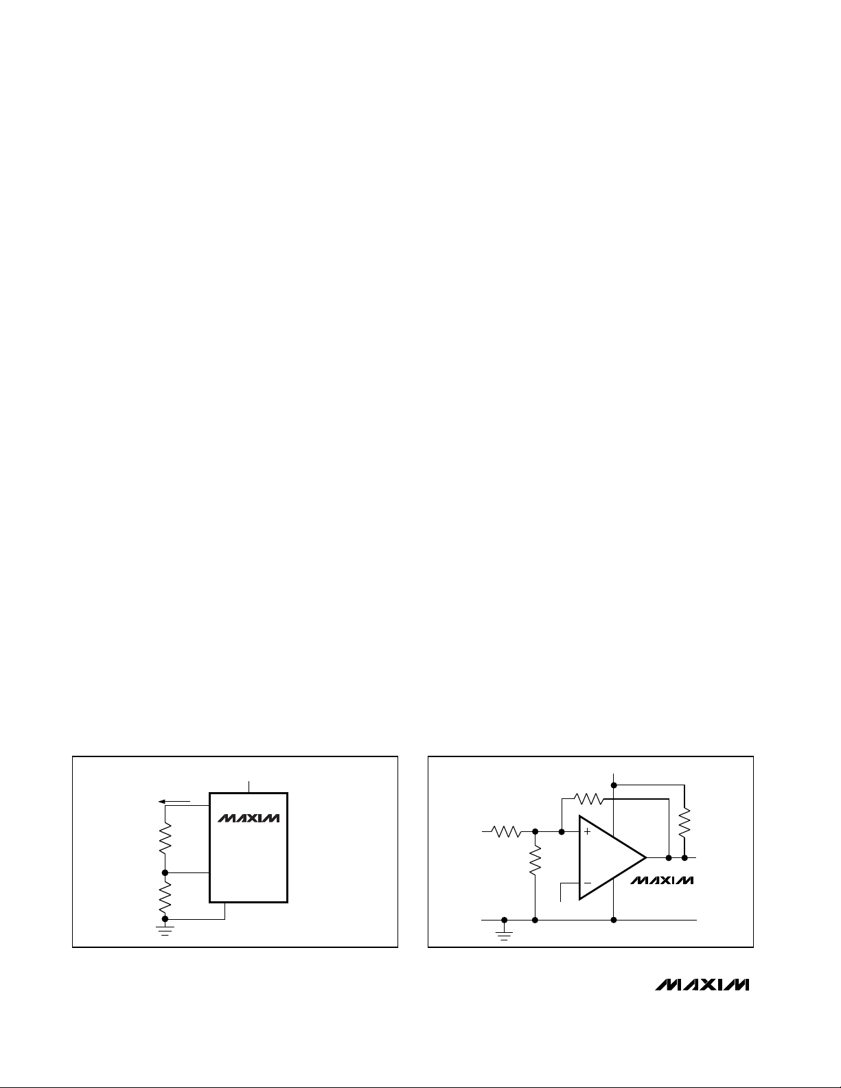
Figure 1 shows a typical comparator application that
monitors VCCat 1.6V. Resistor divider R1/R2 sets the
voltage trip point (V
TRIP
) at 1.6V. As VCCdrops below
1.6V and approaches 1V, the reference voltage typically falls below the divider voltage (V+). This causes the
comparator output to change state. If OUT’s state must
be maintained under these conditions, a latching circuit
is required.
Comparator Output
The MAX965–MAX970 contain a unique slew-ratecontrolled output stage capable of rail-to-rail operation
with an external pull-up resistor. Typical comparators
consume orders of magnitude more current during
switching than during steady-state operation. With the
MAX965 family of comparators, during an output transition from high to low, the output slew rate is limited to
minimize switching current.
Voltage Reference
With VCCgreater than 1.6V but less than 5.5V, the internal 1.235V bandgap reference is ±1.5% accurate over
the commercial temperature range and ±2.5% accurate over the extended temperature range. The REF
output is typically capable of sourcing 50µA. To reduce
reference noise or to provide noise immunity, bypass
REF with a capacitor (0.1nF to 0.1µF).
Noise Considerations
The comparator has an effective wideband peak-topeak noise of around 10µV. The voltage reference has
peak-to-peak noise approaching 1.0mV with a 0.1µF
bypass capacitor. Thus, when a comparator is used
with the reference, the combined peak-to-peak noise is
about 1.0mV. This, of course, is much higher than the
individual components’ RMS noise. Avoid capacitive
coupling from any output to the reference pin. Crosstalk
can significantly increase the references’ actual noise.
__________Applications Information
Hysteresis
Many comparators oscillate in the linear region of operation because of noise or undesired parasitic feedback. This tends to occur when the voltage on one
input is equal or very close to the voltage on the other
input. The MAX965–MAX970 have internal hysteresis to
counter parasitic effects and noise. In addition, with the
use of external resistor, the MAX965/MAX967/
MAX968/MAX969’s hysteresis can be programmed to
as much as ±50mV (see the section Adding Hysteresis
to the MAX965/MAX967/MAX968/MAX969).
The hysteresis in a comparator creates two trip points:
one for the rising input voltage and one for the falling
input voltage (Figure 2). The difference between the trip
points is the hysteresis. When the comparator’s input
voltages are equal, the hysteresis effectively causes
one comparator input voltage to move quickly past the
other, thus taking the input out of the region where
oscillation occurs.
THRESHOLDS
OUT
IN-
IN+
V
HB
HYSTERESIS
BAND
V
REF
- V
HYST
Figure 2. Threshold Hysteresis Band
REF
GND
V
CC
V
TRIP
= 1.22 + 1
V
CC
V
REF
OUT
R1 47k
R2 150k
V+
V
CC
V+
t
1.6V
1.0V
100k
MAX965
R1
R2
R1 = x R2
- 1
V
TRIP
1.22
Figure 1. Operation below 1.6V
_______________________________________________________________________________________ 9
Page 10
MAX965–MAX970
Single/Dual/Quad, Micropower,
Ultra-Low-V oltage, Rail-to-Rail I/O Comparators
10 ______________________________________________________________________________________
HYST
REF
GND
V
CC
R1
R2
MAX965
MAX967
MAX968
MAX969
+1.6V TO +5.5V
I
REF
Figure 3. Programming the HYST Pin
GND
V
CC
V
CC
OUT
R3
R1
R2
R4
V
REF
V
IN
MAX966
MAX970
Figure 4. External Hysteresis
Figure 2 illustrates the case in which IN- has a fixed
voltage applied, and IN+ is varied. If the inputs were
reversed, the figure would be the same, except with an
inverted output.
Adding Hysteresis to the
MAX965/MAX967/MAX968/MAX969
To add hysteresis to the MAX965/MAX967/MAX968/
MAX969, connect resistor R1 between REF and HYST,
and connect resistor R2 between HYST and GND
(Figure 3). If additional hysteresis is not required,
connect HYST to REF. When hysteresis is added, the
upper and lower trip points change by the same
amount in opposite directions. The hysteresis band (the
difference between the upper and lower trip points,
VHB) is approximately twice the voltage between HYST
and REF. The HYST input voltage range is from REF
down to (REF - 50mV). This yields a hysteresis band
from ±1mV to a maximum of ±50mV. Calculate the values of R1 and R2 for the desired hysteresis band with
the following formulas:
R1 = VHB/ I
REF
R2 = (V
REF
- VHB) / I
REF
where I
REF
(the current sourced by the reference) does
not exceed the REF source capability (12µA typical),
and is significantly larger than the HYST leakage current (5nA typical). I
REF
values between 0.1µA and 4µA
are good choices. If 2.4MΩ is chosen for R2 (I
REF
=
0.5µA), the equation for R1 and VHBcan be approximated as:
R1(kΩ) = 2 x VHB(mV)
In the MAX967/MAX968/MAX969, the HYST pin programs the same hysteresis for all comparators in the
package.
Due to the internal structure of the input developed for
ultra-low-voltage operation, the hysteresis band varies
with common-mode voltage. The graph Programmed
Hysteresis vs. Common-Mode Voltage in the Typical
Operating Characteristics shows this variation. Notice
that the hysteresis band increases to almost twice the
calculated value toward the ends of the common-mode
range. This is apparent only when programming additional hysteresis using the HYST pin. The hysteresis
band is constant when HYST is connected to REF.
Adding Hysteresis to the MAX966/MAX970
The MAX966/MAX970 do not have a HYST pin for programming hysteresis. Hysteresis can be generated with
three resistors using positive feedback (Figure 4). This
method generally draws more current than the method
using the HYST pin on the MAX965/MAX967/MAX968/
MAX969. Also, the positive feedback method slows
hysteresis response time. Use the following procedure
to calculate the resistor values:
1) Select R3. The leakage current of IN+ is under 5nA,
so the current through R3 should be at least 500nA
to minimize errors caused by leakage current. The
current through R3 at the trip point is (V
REF
- V
OUT
) /
R3. Taking into consideration the two possible output states and solving for R3 yields two formulas:
R3 = V
REF
/ 500nA
and
R3 = (V
REF
- VCC) / 500nA
Use the smaller of the two resulting resistor values.
For example, if V
REF
= 1.2V and VCC= 5.0V, then
the two resistor values are 2.4MΩ and 7.6mΩ. For
R3, choose the 2.2MΩ standard value.
2) Choose the hysteresis band required (VHB). For this
example, choose 50mV.
Page 11

MAX965–MAX970
Single/Dual/Quad, Micropower,
Ultra-Low-V oltage, Rail-to-Rail I/O Comparators
______________________________________________________________________________________ 11
3) Calculate R1: R1 = (R3 + R4) x (VHB/ VCC). Putting
in the values for this example, R1 = (2.2MΩ + 10k) x
(50mV / 5.0V) = 22.1kΩ.
4) Choose the trip point for VINrising. This is the
threshold voltage where the comparator output transitions from low to high as VINrises above the trip
point. For this example, choose 3.0V.
5) Calculate R2 as follows:
where V
THR
is the rising-voltage trip threshold.
Choose a standard value of 15kΩ.
6) Verify trip voltages and hysteresis as follows:
where V
THR
is the rising-voltage trip point, and V
THF
is the falling-voltage trip point.
Circuit Layout and Bypassing
Power-supply bypass capacitors are not needed if supply impedance is low, but 100nF bypass capacitors
should be used when supply impedance is high or
when supply leads are long. Minimize signal lead
lengths to reduce stray capacitance between the input
and output that might cause instability.
IR Receiver
Figure 5 shows an application using the MAX965 as an
infrared receiver. The infrared photodiode creates a
current relative to the amount of infrared light present.
This current creates a voltage across R1. When this
voltage level crosses the reference voltage applied to
the inverting input, the output transitions. Optional R3
provides additional hysteresis for noise immunity.
2-Cell to TTL Logic-Level Shifter
Figure 6 shows an application using the MAX965
to convert a 2-cell voltage-level signal into a TTLcompatible signal. The supply voltage for the comparator comes from the 2-cell supply. The output is pulled
up to a 5V supply.
V ri g
V V x R x
R R R R
V falling
V V
R x V
R R
Hysteresis V V
IN
THR REF
IN
THF THR
CC
THR THF
sin :
:
= + +
+
= −
+
= −
1
111
213 4
1
3 4
R
V
V x R R R R
R
V
x k k M k
k
THR
REF
2
1
1
1
1
1
3 4
2
1
3 0
1 2 22
1
22
1
2 2 10
14 76
=
− −
+
=
− −
+
=
.
.
.
.
GND
V
CC
V
CC
V
CC
V
CC
0.1µF
OUT
R3
R
D
R
PULL-UP
REF
MAX965
HYST
Figure 5. IR Receiver
GND
V
CC
+5V
2 CELLS
0.1µF
OUT
INPUT
REF
MAX965
HYST
Figure 6. 2-Cell to TTL Logic-Level Translator
Page 12
Maxim cannot assume responsibility for use of any circuitry other than circuitry entirely embodied in a Maxim product. No circuit patent licenses are
implied. Maxim reserves the right to change the circuitry and specifications without notice at any time.
12 __________________Maxim Integrated Products, 120 San Gabriel Drive, Sunnyvale, CA 94086 (408) 737-7600
© 1997 Maxim Integrated Products Printed USA is a registered trademark of Maxim Integrated Products.
MAX965–MAX970
Single/Dual/Quad, Micropower,
Ultra-Low-V oltage, Rail-to-Rail I/O Comparators
TRANSISTOR COUNTS:
MAX965 = 216
MAX966 = 190
MAX967/MAX968 = 299
MAX969 = 465
MAX970 = 380
___________________Chip Information
PART TEMP. RANGE PIN-PACKAGE
MAX969EEE -40°C to +85°C 16 QSOP
MAX969ESE
-40°C to +85°C 16 Narrow SO
MAX968EUA -40°C to +85°C 8 µMAX
MAX968ESA
-40°C to +85°C 8 SO
MAX970ESD
-40°C to +85°C 14 SO
MAX970EEE -40°C to +85°C 16 QSOP
_Ordering Information (continued)
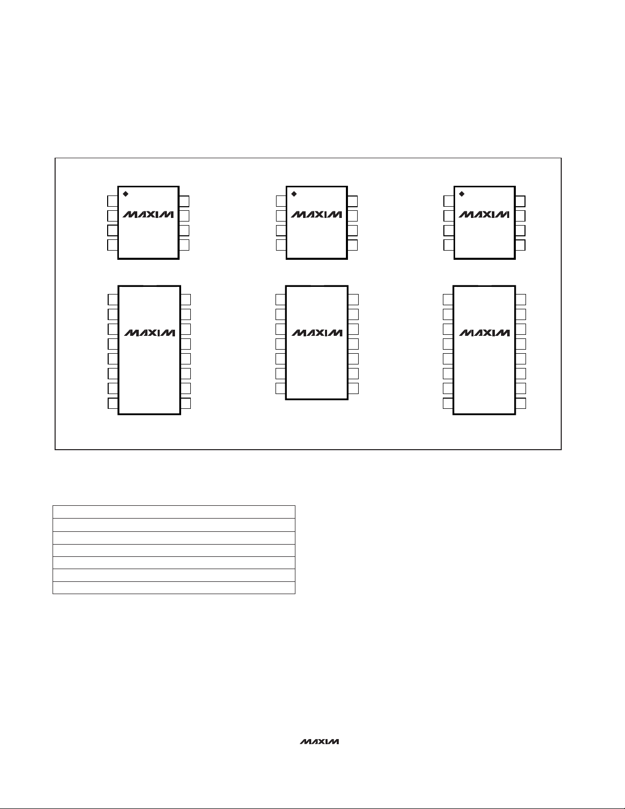
__________________________________________________________Pin Configurations
14
13
12
11
10
9
8
1
2
3
4
5
6
7
OUTC
OUTD
GND
IND+INA-
V
CC
OUTA
OUTB
MAX970
INDINC+
INC-
INB+
INB-
INA+
SO
TOP VIEW
16
15
14
13
12
11
10
9
1
2
3
4
5
6
7
8
OUTC
OUTD
GND
IND+INA-
V
CC
OUTA
OUTB
MAX969
IND-
INC+
INC-
HYST
REF
INB+
INB-
INA+
SO/QSOP
16
15
14
13
12
11
10
9
1
2
3
4
5
6
7
8
OUTC
OUTD
GND
IND+INA-
V
CC
OUTA
OUTB
MAX970
INDINC+
INC-
N.C.
N.C.
INB+
INB-
INA+
QSOP
1
2
3
4
OUT
V
CC
REF
HYSTIN-
IN+
N.C.
GND
MAX965
SO/µMAX
SO/µMAX
SO/µMAX
8
7
6
5
1
2
3
4
OUTB
V
CC
INB+
INB-INA-
INA+
GND
OUTA
MAX966
8
7
6
5
1
2
3
4
OUTB
V
CC
REF
HYSTINB+
(INB-)
INA+
GND
OUTA
MAX967
MAX968
8
7
6
5
( ) ARE FOR MAX968 ONLY.
 Loading...