

Page 1
General Description
The MAX9655/MAX9656 dual SCART switches route
video signals between a set-top box decoder chip and
two external SCART connectors. Under the control of the
TV_SEL logic input, the MAX9655 selects whether the
CVBS and RGB signals from the encoder or the VCR
SCART are routed to the TV SCART. The CVBS signal
from the encoder is always routed to the VCR SCART.
The MAX9656 is similar to the MAX9655 except that
under the control of the VCR_SEL logic input, the
MAX9656 selects whether the CVBS signal from the
encoder or the TV SCART is routed to the VCR SCART.
The MAX9656 also features a low-power shutdown
mode, in which quiescent current falls to 35µA.
The incoming video signals must be AC-coupled to the
inputs, which have sync-tip clamps to set the internal
DC level. After the input stages, multiplexers select
which video signals are routed to the reconstruction filters and output amplifiers. The reconstruction filters are
optimized for standard-definition signals and typically
have ±1dB passband flatness out to 9.5MHz and 47dB
attenuation at 27MHz.
The amplifiers have 2V/V gain, and the outputs can be
DC-coupled to a 75Ω load, which is the equivalent of
two video loads, or AC-coupled to a 150Ω load.
Applications
SCART Set-Top Boxes
Features
♦ Dual SCART Support for Video Signals
♦ Supports CVBS Input from TV SCART (MAX9656)
♦ Reconstruction Filters with 9.5MHz Passband and
47dB Attenuation at 27MHz
♦ Fixed Gain of 2V/V
♦ Input Sync-Tip Clamps
♦ 2.7V to 3.6V Single-Supply Operation
MAX9655/MAX9656
Low-Power Video Switches
for Dual SCART Connectors
________________________________________________________________
Maxim Integrated Products
1
19-4238; Rev 0; 8/08
For pricing, delivery, and ordering information, please contact Maxim Direct at 1-888-629-4642,
or visit Maxim’s website at www.maxim-ic.com.
UNKNOWN
BIAS
ENC_CVBS_IN
300mV
ENC_R_IN
TV_G_OUT
ENC_G_IN
ENC_B_IN
TV_B_OUT
TV_CVBS_OUT
TV_R_OUT
VCR_CVBS_OUT
VCR_CVBS_IN
VCR_R_IN
VCR_G_IN
VCR_B_IN
TV_SEL
TV_SEL
0
1
0
1
0
1
0
1
0
V
DD
GND
MAX9655
LPF
BUFFER
CLAMPREF
LPF
BUFFER
CLAMPREF
LPF
BUFFER
CLAMPREF
LPF
BUFFER
CLAMPREF
2V/V
2V/V
2V/V
2V/V
2V/V
LPF
BUFFER
CLAMPREF
Functional Diagram
Ordering Information
Note: All devices are specified over the -40°C to +125°C operating temperature range.
+
Denotes a lead-free/RoHS-compliant package.
*
Future product—contact factory for availability.
Pin Configurations and Typical Application Circuits appear
at end of data sheet.
PART PIN-PACKAGE
MAX9655AEE+ 16 QSOP No
MAX9656AEP+* 20 QSOP Yes
TV SCART CVBS
RETURN SUPPORT
Page 2
MAX9655/MAX9656
Low-Power Video Switches
for Dual SCART Connectors
2 _______________________________________________________________________________________
ABSOLUTE MAXIMUM RATINGS
ELECTRICAL CHARACTERISTICS
(VDD= 3.3V, V
GND
= 0, V
SHDN
= VDD, VCR_SEL = VDD, TV_SEL = VDD, RL= 150Ω to GND, TA= T
MIN
to T
MAX
, unless otherwise
noted. Typical values are at T
A
= +25°C.) (Note 1)
Stresses beyond those listed under “Absolute Maximum Ratings” may cause permanent damage to the device. These are stress ratings only, and functional
operation of the device at these or any other conditions beyond those indicated in the operational sections of the specifications is not implied. Exposure to
absolute maximum rating conditions for extended periods may affect device reliability.
Supply Voltage
V
DD
to GND...........................................................-0.3V to +4V
All Video and Logic Input Pins..................(GND - 0.3V) to +4V
Duration of Output Short Circuit to V
DD
or GND ........Continuous
Continuous Input Current
All Video and Logic Input Pins .....................................±20mA
Continuous Power Dissipation (T
A
= +70°C)
16-Pin QSOP (derate 8.3mW/°C above +70°C)............667mW
20-Pin QSOP (derate 9.1mW/°C above +70°C)............727mW
Operating Temperature Range .........................-40°C to +125°C
Junction Temperature......................................................+150°C
Storage Temperature Range .............................-65°C to +150°C
Lead Temperature (soldering, 10s) .................................+300°C
PARAMETER SYMBOL CONDITIONS MIN TYP MAX UNITS
Supply Voltage Range V
Quiescent Supply Current I
Shutdown Supply Current I
Input Voltage Unselected input VDD/3 V
Input Resistance
Sync-Tip Clamp Level V
Input Voltage Range
Sync Crush
Input Clamping Current 12µA
Maximum Input Source
Resistance
DC Voltage Gain A
DC Gain Mismatch Guaranteed by output-voltage swing -2 +2 %
Output Level Measured at output, C
Output-Voltage Swing
DD
DD
SHDN
Guaranteed by power-supply rejection test 2.7 3.3 3.6 V
No load 21 45 mA
V
= 0 (MAX9656 only) 35 µA
SHDN
Unselected input 222 kΩ
CLP
Guaranteed by outputvoltage swing
Sync-tip clamp; percentage reduction in
sync pulse (0.3V
clamping current measurement
RL = 150Ω to GND
V
(Note 2) V
Measured at output, VDD = 2.7V, V
to (V
V
CLP
CLP
Measured at output, VDD = 2.7V, V
to (V
V
CLP
CLP
Measured at output, VDD = 3.0V, VIN =
to (V
V
CLP
CLP
Measured at output, VDD = 3.0V, V
to (V
V
CLP
CLP
Measured at output, V
to (V
V
CLP
CLP
0.23 0.3 0.39 V
2.7V ≤ VDD ≤ 3.6V 1.05
3.0V ≤ V
); guaranteed by input
P-P
≤ 3.6V 1.2
DD
2%
300 Ω
VDD = 2.7V, 0V ≤ V
≤ 1.05V
= 3.0V, 0V ≤ V
DD
≤ 1.2V
= 0.1µF to GND 0.218 0.3 0.39 V
IN_
+1.05V), RL = 150Ω to -0.2V
+1.05V), RL = 150Ω to VDD/2
+1.2V), RL = 150Ω to -0.2V
+1.2V), RL = 150Ω to VDD/2
= 3.135V, V
DD
+1.05V), RL = 75Ω to -0.2V
IN
IN
IN
=
=
=
IN
IN
1.96 2 2.04
IN
1.96 2 2.04
2.1
2.1
2.4
2.4
=
2.1
V
V/V
V
P-P
P-P
Page 3
MAX9655/MAX9656
Low-Power Video Switches
for Dual SCART Connectors
_______________________________________________________________________________________ 3
ELECTRICAL CHARACTERISTICS (continued)
(VDD= 3.3V, V
GND
= 0, V
SHDN
= VDD, VCR_SEL = VDD, TV_SEL = VDD, RL= 150Ω to GND, TA= T
MIN
to T
MAX
, unless otherwise
noted. Typical values are at T
A
= +25°C.) (Note 1)
Note 1: All devices are 100% production tested at T
A
= +25°C. Specifications over temperature limits are guaranteed by design.
Note 2: Voltage gain (A
V
) is a two-point measurement in which the output-voltage swing is divided by the input-voltage swing.
PARAMETER SYMBOL CONDITIONS MIN TYP MAX UNITS
Output Short-Circuit Current
Output Resistance R
Power-Supply Rejection Ratio
Standard-Definition
Reconstruction Filter
Differential Gain DG
Differential Phase DP
Group-Delay Distortion 100kHz ≤ f ≤ 5MHz, outputs are 2V
Peak Signal to RMS Noise 100kHz ≤ f ≤ 5MHz 71 dB
2T Pulse Response 2T = 200ns 0.2 K%
2T Bar Response
Short to GND (sourcing) 140
(sinking) 70
DD
= 1.5V, -10mA ≤ I
P-P
= 2V
= 2V
, reference frequency is
P-P
, reference
P-P
≤ +10mA 0.2 Ω
LOAD
f = 5.5MHz 0.1
f = 9.5MHz -1
f = 10MHz -3
f = 27MHz -47
P-P
OUT
Short to V
V
OUT
2.7V ≤ VDD ≤ 3.6V 48 64
f = 1MHz, 100mV
V
OUT
100kHz, ±1dB passband flatness
V
OUT
frequency is 100kHz
5-step modulated staircase of 129mV step
size and 286mV peak-to-peak subcarrier
amplitude, f = 4.43MHz
5-step modulated staircase of 129mV step
size and 286mV peak-to-peak subcarrier
amplitude, f = 4.43MHz
2T = 200ns; bar time is 18µs; the beginning
2.5% and the ending 2.5% of the bar time
are ignored
20
9.5 MHz
0.4 %
0.45 deg
9ns
0.2 K%
mA
dB
dB
2T = 200ns; bar time is 18µs; the beginning
2T Pulse-to-Bar K Rating
Nonlinearity 5-step staircase 0.1 %
Output Impedance f = 5.5MHz 8.07 Ω
All-Hostile Crosstalk
Output-to-Input Crosstalk f = 30MHz -68 dB
LOGIC SIGNALS (MAX9655: TV_SEL, MAX9656: TV_SEL, VCR_SEL, SHDN)
Logic-Low Threshold V
Logic-High Threshold V
Logic Input Current I
2.5% and the ending 2.5% of the bar time
are ignored
f = 15kHz -82
f = 4.43MHz -78
TA = +25°C
IL
TA = +25°C
IH
TA = +25°C10µA
IN
0.7 x
V
DD
0.3 K%
0.3 x
V
DD
dB
V
V
Page 4
MAX9655/MAX9656
Low-Power Video Switches
for Dual SCART Connectors
4 _______________________________________________________________________________________
Typical Operating Characteristics
(VDD= 3.3V, V
GND
= 0, V
SHDN
= VDD, RL= 150Ω to GND, TA= +25°C.)
SMALL-SIGNAL GAIN
vs. FREQUENCY
MAX9655 toc01
FREQUENCY (Hz)
GAIN (dB)
10M1M
-45
-40
-35
-30
-25
-20
-15
-10
-5
0
5
10
-50
100k 100M
VIN 50mV
P-P
NOTE: GAIN IS NORMALIZED TO 0dB
SMALL-SIGNAL GAIN FLATNESS
vs. FREQUENCY
MAX9655 toc02
FREQUENCY (Hz)
GAIN (dB)
10M1M
-6
-5
-4
-3
-2
-1
0
1
2
3
-7
100k 100M
VIN 50mV
P-P
NOTE: GAIN IS NORMALIZED TO 0dB
LARGE-SIGNAL GAIN
vs. FREQUENCY
MAX9655 toc03
FREQUENCY (Hz)
GAIN (dB)
10M1M
-45
-40
-35
-30
-25
-20
-15
-10
-5
0
5
10
-50
100k 100M
VIN 1V
P-P
NOTE: GAIN IS NORMALIZED TO 0dB
LARGE-SIGNAL GAIN FLATNESS
vs. FREQUENCY
MAX9655 toc04
FREQUENCY (Hz)
GAIN (dB)
10M1M
-6
-5
-4
-3
-2
-1
0
1
2
3
-7
100k 100M
VIN 1V
P-P
NOTE: GAIN IS NORMALIZED TO 0dB
VIDEO CROSSTALK
vs. FREQUENCY
MAX9655 toc05
FREQUENCY (Hz)
GAIN (dB)
10M1M
-100
-80
-60
-40
-20
0
-120
100k 100M
ALL-HOSTILE
1 ADJACENT CHANNEL
2 ADJACENT CHANNELS
VIN 1V
P-P
NOTE: GAIN IS NORMALIZED TO 0dB
VIDEO GROUP DELAY DISTORTION
vs. FREQUENCY
MAX9655 toc06
FREQUENCY (Hz)
GROUP DELAY (ns)
10M1M
10
20
30
40
50
60
70
80
90
100
110
120
0
100k 100M
VIN 1V
P-P
NOTE: GAIN IS NORMALIZED TO 0dB
Page 5
MAX9655/MAX9656
Low-Power Video Switches
for Dual SCART Connectors
_______________________________________________________________________________________
5
Typical Operating Characteristics (continued)
(VDD= 3.3V, V
GND
= 0, V
SHDN
= VDD, RL= 150Ω to GND, TA= +25°C.)
VIDEO PSRR
vs. FREQUENCY
0
VDD = 3.3V + 100mV
-10
-20
-30
-40
PSRR (dB)
-50
-60
-70
-80
100k 100M
P-P
FREQUENCY (Hz)
DIFFERENTIAL GAIN
0.1
0
-0.1
-0.2
-0.3
-0.4
-0.5
DIFFERENTIAL GAIN (%)
103245
DIFFERENTIAL PHASE
0.8
0.6
0.4
0.2
0
-0.2
-0.4
DIFFERENTIAL PHASE (deg)
103245
VOLTAGE GAIN
vs. TEMPERATURE
2.10
10M1M
f = 3.58MHz
f = 3.58MHz
MAX9655 toc07
MAX9655 toc09
2.08
2.06
2.04
2.02
2.00
1.98
VOLTAGE GAIN (V/V)
1.96
1.94
1.92
1.90
-50 -25 0 25 50 75 100 125
TEMPERATURE (°C)
DIFFERENTIAL GAIN
0.1
0
-0.1
-0.2
-0.3
-0.4
-0.5
DIFFERENTIAL GAIN (%)
103245
DIFFERENTIAL PHASE
0.8
0.6
0.4
0.2
0
-0.2
-0.4
DIFFERENTIAL PHASE (deg)
103245
f = 4.43MHz
f = 4.43MHz
MAX9655 toc08
MAX9655 toc10
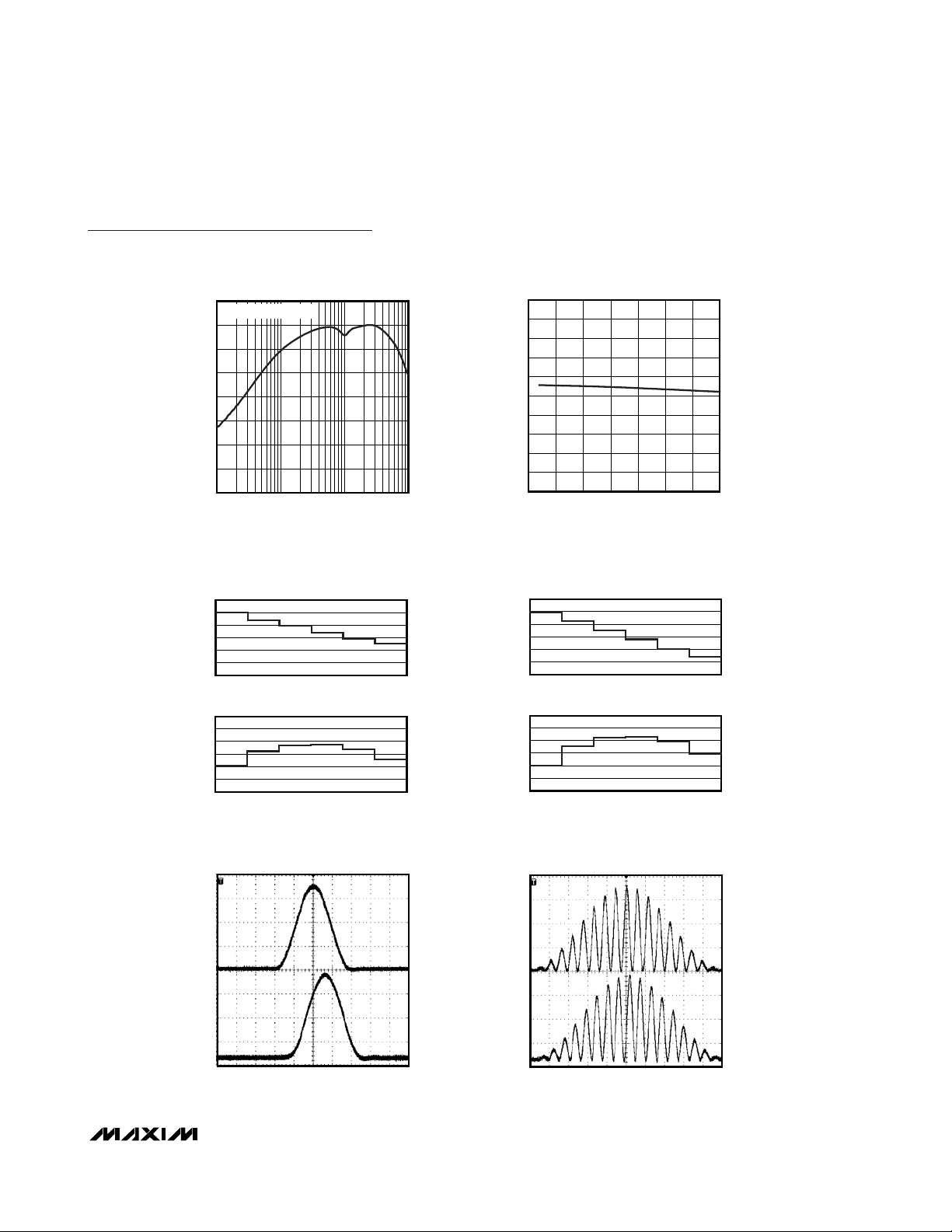
2T RESPONSE
100ns/div
MAX9655 toc11
IN
200mV/div
OUT
400mV/div
12.5T RESPONSE
400ns/div
MAX9655 toc12
IN
200mV/div
OUT
400mV/div
Page 6

MAX9655/MAX9656
Low-Power Video Switches
for Dual SCART Connectors
6 _______________________________________________________________________________________
Typical Operating Characteristics (continued)
(VDD= 3.3V, V
GND
= 0, V
SHDN
= VDD, RL= 150Ω to GND, TA= +25°C.)
10μs/div
NTC-7 VIDEO TEST SIGNAL
IN
500mV/div
MAX9655 toc13
OUT
1V/div
2ms/div
FIELD SQUARE WAVE
IN
500mV/div
MAX9655 toc14
OUT
1V/div
0.26
0.30
0.28
0.34
0.32
0.38
0.36
0.40
-50 0 25-25 50 75 100 125
VIDEO SYNC-TIP CLAMP VOLTAGE
vs. TEMPERATURE
MAX4617 toc15
TEMPERATURE (°C)
SYNC-TIP CLAMP VOLTAGE (V)
0.90
0.94
0.92
0.98
0.96
1.02
1.00
1.04
-50 0 25-25 50 75 100 125
VIDEO SYNC-TIP CLAMP CURRENT
vs. TEMPERATURE
MAX4617 toc16
TEMPERATURE (°C)
SYNC-TIP CLAMP CURRENT (μA)
-100
0
100
200
300
400
500
0 0.40.2 0.6 0.8 1.0 1.2 1.4 1.6
SYNC-TIP CLAMP CURRENT
vs. INPUT VOLTAGE
MAX9655 toc17
INPUT VOLTAGE (V)
SYNC-TIP CLAMP CURRENT (μA)
20.0
20.5
21.5
21.0
22.5
22.0
23.0
-50 0 25-25 50 75 100 125
QUIESCENT SUPPLY CURRENT
vs. TEMPERATURE
MAX4617 toc18
TEMPERATURE (°C)
QUIESCENT SUPPLY CURRENT (mA)
Page 7

MAX9655/MAX9656
Low-Power Video Switches
for Dual SCART Connectors
_______________________________________________________________________________________ 7
Detailed Description
A MAX9655 or a MAX9656 can comprise the video portion of a low-cost, dual SCART solution in set-top boxes
with a subset of the full SCART functions. The
MAX9655/MAX9656 select whether the CVBS, red,
green, and blue video signals from the encoder or the
VCR SCART are routed to the TV SCART. The
MAX9655/MAX9656 support the output of one CVBS
signal to the VCR SCART. In the MAX9655, the CVBS
signal from the encoder is routed to the VCR SCART.
In the MAX9656, the CVBS signal routed to the VCR
SCART can come from the encoder or TV SCART. In
the typical usage case, the VCR (or DVD recorder)
records a television program from the set-top box. In
such a case, the encoder would be the source of the
CVBS signal. Support for the TV SCART CVBS return
path is useful when a person wants to record on his
VCR (or more likely DVD recorder) a television program
received through the television’s antenna. The television program is transmitted from the television to the
set-top box and then to the VCR.
Both the MAX9655 and MAX9656 have integrated
reconstruction filters so that when the encoder video
signals are routed to the TV SCART or the VCR SCART,
the steps and spikes left by the video digital-to-analog
converter (DAC) are smoothed away. Although the
incoming video signals from the VCR SCART are
assumed to be filtered already, the reconstruction filter
has wide enough bandwidth so that the video signals
from the VCR SCART are not degraded.
Pin Description
PIN
MAX9655 MAX9656
1 2 ENC_B_IN Encoder Blue Video Input. AC-couple the signal through a 0.1µF capacitor.
2 3 ENC_G_IN Encoder Green Video Input. AC-couple the signal through a 0.1µF capacitor.
3 4 ENC_R_IN Encoder Red Video Input. AC-couple the signal through a 0.1µF capacitor.
4 5 ENC_CVBS_IN Encoder Composite Video Input. AC-couple the signal through a 0.1µF capacitor.
5 6 VCR_B_IN VCR SCART Blue Video Input. AC-couple the signal through a 0.1µF capacitor.
6 7 VCR_G_IN VCR SCART Green Video Input. AC-couple the signal through a 0.1µF capacitor.
7 8 VCR_R_IN VCR SCART Red Video Input. AC-couple the signal through a 0.1µF capacitor.
8 9 VCR_CVBS_IN V C R S C ART C om p osi te V i d eo Inp ut. AC - coup l e the si g nal thr oug h a 0.1µF cap aci tor .
9 11 GND Ground
10 13 VCR_CVBS_OUT VCR SCART Composite Video Output. The sync tip is biased at 0.3V.
11 14 TV_CVBS_OUT TV SCART Composite Video Output. The sync tip is biased at 0.3V.
12 15 TV_R_OUT TV SCART Red Video Output. The sync tip is biased at 0.3V.
13 16 TV_G_OUT TV SCART Green Video Output. The sync tip is biased at 0.3V.
14 17 TV_B_OUT TV SCART Blue Video Output. The sync tip is biased at 0.3V.
15 18 TV_SEL
16 19 V
— 1 TV_CVBS_IN
— 10 N.C. No Connection. Not internally connected.
—12 SHDN
— 20 VCR_SEL
NAME FUNCTION
TV SCART Output Selection. Connect to GND to route the encoder video signals
to the TV SCART outputs. Connect to VDD to route the VCR SCART video signals
to the TV SCART outputs.
DD
Positive Power Supply. Bypass with 0.1µF ceramic capacitors to GND.
Television SCART Composite Video Input. AC-couple the signal through a 0.1µF
capacitor.
Active-Low Shutdown Logic Input. Connect to GND to place device in shutdown.
Connect to V
VCR SCART Output Selection. Connect to GND to route ENC_CVBS_IN to the
VCR SCART CVBS output. Connect to VDD to route TV_CVBS_IN to the VCR
SCART CVBS output.
for normal operation.
DD
Page 8

MAX9655/MAX9656
Low-Power Video Switches
for Dual SCART Connectors
8 _______________________________________________________________________________________
The incoming video signals can have any DC bias
because the input sync-tip clamps restore the
DC level. The output amplifiers have a gain of 2V/V.
The MAX9655/MAX9656 operate from a single 3.3V
supply and consume low quiescent power and low
average power. In addition, the MAX9656 also has
shutdown mode.
Operating Modes
TV_SEL controls whether the encoder or VCR video signals are sent to the TV SCART. See Table 1.
On the MAX9656, VCR_SEL controls whether the CVBS
signal from the TV SCART or the encoder is sent to the
VCR SCART. SHDN controls whether the device is on
or off. See Tables 2 and 3. In shutdown, the outputs of
the MAX9656 are high impedance.
Input
Every video signal must be AC-coupled to the
MAX9655/MAX9656 through 0.1µF capacitors. The
MAX9655/MAX9656 have sync-tip clamps and bias circuits to restore the DC level of the video signal after the
input coupling capacitor. When a video input is selected, the input has a sync-tip clamp, which accepts
video signals that have sync pulses or that reach their
minimum level during sync. Composite video with
blanking and sync (CVBS) is an example of a video signal with sync pulses. The red, green, and blue signals
in an RGBS signal set are examples of signals that
return to their blank level during sync. The sync-tip voltage is internally set to 300mV.
When a video input is not selected, the inputs to the
MAX9655 and the MAX9656 do not distort the video
signal in case the video source is driving video signals
to another video circuit such as a video multiplexer.
The inputs are biased at VDD/3, which is sufficiently
above ground so that the ESD diodes never forward
bias as the video signal changes. The input resistance
is 220kΩ, which presents negligible loading on the
video current DAC. The sole exception to this condition
is ENC_CVBS_IN (MAX9655), in which the input circuit
is always a sync-tip clamp. Table 4 summarizes which
input circuit is active on the inputs of the MAX9655
depending on TV_SEL. Table 5 summarizes which input
circuit is active on the inputs of the MAX9656 depending on TV_SEL and VCR_SEL.
Table 1. TV_SEL Logic (Applicable to
Both the MAX9655 and the MAX9656)
Table 2. VCR_SEL Logic (Only Applicable
to the MAX9656)
Table 3. SHDN Logic (Only Applicable to
the MAX9656)
Table 4. MAX9655 Input Circuit of Input as Determined by State of TV_SEL
LOGIC STATE MODE
Low
High
Encoder video signals are routed to the
TV SCART.
VCR SCART video signals are routed to
the TV SCART.
LOGIC STATE MODE
Low
High
CVBS signal from encoder is routed to the
VCR SCART.
CVBS signal from the TV SCART is routed
to the VCR SCART.
LOGIC STATE MODE
Low Off
High On
INPUT
ENC_B_IN Sync-tip clamp Bias
ENC_G_IN Sync-tip clamp Bias
ENC_R_IN Sync-tip clamp Bias
ENC_CVBS_IN Sync-tip clamp Sync-tip clamp
VCR_B_IN Bias Sync-tip clamp
VCR_G_IN Bias Sync-tip clamp
VCR_R_IN Bias Sync-tip clamp
VCR_CVBS_IN Bias Sync-tip clamp
INPUT CIRCUIT
(TV_SEL = LOW)
INPUT CIRCUIT
(TV_SEL = HIGH)
Page 9

MAX9655/MAX9656
Low-Power Video Switches
for Dual SCART Connectors
_______________________________________________________________________________________ 9
When the MAX9656 is in shutdown, its inputs are
biased at the same voltage and present the same input
resistance as unselected inputs.
Video Filter
The MAX9655/MAX9656 video filter features ±1dB
passband out to 9.5MHz and 47dB attenuation at
27MHz, making the filter suitable for standard-definition
video signals from all sources (e.g., broadcast and
DVD). Broadcast video signals are channel limited:
NTSC signals have 4.2MHz bandwidth, and PAL signals have 5MHz bandwidth. Video signals from a DVD
player, however, are not channel limited; so the bandwidth of DVD video signals can approach the Nyquist
limit of 6.75MHz. Recommendation: ITU-R BT.601-5
specifies 13.5MHz as the sampling rate for standarddefinition video. Therefore, the maximum bandwidth of
the signal is 6.75MHz. To ease the filtering requirements, most modern video systems oversample by two
times, clocking the video current DAC at 27MHz.
Outputs
The video output amplifiers can both source and sink
load current, allowing output loads to be DC- or ACcoupled. The amplifier output stage needs approximately 300mV of headroom from either supply rail. The
devices have an internal level-shift circuit that positions
the sync tip at approximately 300mV at the output.
If the supply voltage is greater than 3.135V (5% below
a 3.3V supply), each amplifier can drive two DC-coupled video loads to ground. If the supply is less than
3.135V, each amplifier can drive only one DC-coupled
or AC-coupled video load.
Applications Information
Audio Switch for Dual SCART Connectors
In addition to video signals, SCART connectors also
support left and right audio signals that are full duplex.
Figure 1 shows a matching audio switch for the
MAX9655. Notice that it can be made from low-cost,
discrete components. It is assumed that the set-top box
chip generates the left and right audio signals directly,
or the set-top box chip sends an I2S stream to a stereo
audio DAC that generates the left and right audio signals. In both cases, the audio signals are filtered and
amplified by a dual audio op amp before they are presented to the audio switch.
Figure 2 shows a matching audio switch for the
MAX9656. Similar to how the MAX9656 handles video
signals, the audio signals from the set-top box chip or
the audio signals from the TV SCART are routed to the
VCR SCART.
AC-Coupling the Outputs
The outputs can be AC-coupled since the output stage
can source and sink current as shown in Figure 3.
Coupling capacitors should be 220µF or greater to
keep the highpass filter, formed by the 150Ω equivalent
resistance of the video transmission line, to a corner
frequency of 4.8Hz or below. The frame rate of PAL
systems is 25Hz. The corner frequency should be well
below the frame rate.
Table 5. MAX9656 Input Circuit of Input as Determined by State of TV_SEL
Note: VCR_SEL = X (don’t care), except where noted.
INPUT
ENC_B_IN Sync-tip clamp Bias
ENC_G_IN Sync-tip clamp Bias
ENC_R_IN Sync-tip clamp Bias
ENC_CVBS_IN
TV_CVBS_IN
VCR_B_IN Bias Sync-tip clamp
VCR_G_IN Bias Sync-tip clamp
VCR_R_IN Bias Sync-tip clamp
VCR_CVBS_IN Bias Sync-tip clamp
Sync-tip clamp
(VCR_SEL = 0)
Bias
(VCR_SEL = 0)
INPUT CIRCUIT
(TV_SEL = LOW)
Sync-tip clamp (VCR_SEL = 1) Sync-tip clamp (VCR_SEL = 0)
Sync-tip clamp
(VCR_SEL = 1)
(VCR_SEL = 0)
INPUT CIRCUIT
(TV_SEL = HIGH)
Bias
Bias
(VCR_SEL = 1)
Sync-tip clamp
(VCR_SEL = 1)
Page 10

MAX9655/MAX9656
Low-Power Video Switches
for Dual SCART Connectors
10 ______________________________________________________________________________________
Figure 1. Audio Switch for the MAX9655
12V
0.1μF
7
10μF
8
DAC
1
SD ATA
LRCK
MCLK
2
3
U0
4
CS4334
DEMSCLK
10μF
5
DAC
6
3.3V
TV_SEL
10kΩ
JU0
4.7kΩ
+
300kΩ
+
10μF
+
300kΩ
12V
2N3904
12V
4.7kΩ
10kΩ
5.1kΩ
5.1kΩ
TV_SEL
4.7kΩ
2.7nF
4.7kΩ
2.7nF
VCR_SEL
JU1
1.2kΩ
2.7nF
1.2kΩ
2.7nF
3.3V
10kΩ
100kΩ
100kΩ
9, 10, 11
100kΩ
2
1
5
3
12V
16
U2
HEF4053
0.1μF
10μF
15
3
+
10μF
TV
SCART
4
1
6
2
21
2
6
3
4
VCR
SCART
1
21
8
7
15
21
+
10μF
10μF
+
12V
9.5kΩ
180pF
12V
8
4
VCR_SEL
0.1μF
1
U1
1/2 LM833
7
1/2 LM833
2
3
9.5kΩ
180pF
6
5
12V
10kΩ
2N3904
10μF
1MΩ
10μF
1MΩ
10μF
1MΩ
TV_SEL
10μF
1MΩ
+
12V
+
100kΩ
12V
100kΩ
+
100kΩ
12V
100kΩ
+
100kΩ
Page 11

MAX9655/MAX9656
Low-Power Video Switches
for Dual SCART Connectors
______________________________________________________________________________________ 11
Figure 2. Audio Switch for the MAX9656
12V
1MΩ
10μF
+
100kΩ
12V
0.1μF
7
9.5kΩ
180pF
12V
12V
0.1μF
16
10μF
15
3
+
SDATA
DEMSCLK
LRCK
MCLK
9.5kΩ
VCR_SEL
8
4
0.1μF
1
U1
1/2 LM833
7
1/2 LM833
9, 10, 11
TV_SEL
12V
100kΩ
10μF
+
1MΩ
10μF
+
1MΩ
VCR_SEL
12V
10μF
+
1MΩ
3
5
100kΩ
12V
1
2
100kΩ
9, 10, 11
100kΩ
3
5
100kΩ
U2
HEF4053
12V
16
U2
HEF4053
8
7
15
21
0.1μF
15
8
7
15
21
10μF
+
+
10μF
+
10μF
TV
SCART
4
1
6
2
21
2
6
3
VCR
SCART
4
1
21
10μF
8
DAC
1
2
3
U0
4
CS4334
DAC
6
3.3V
TV_SEL
JU0
+
300kΩ
+
10μF
5
+
300kΩ
12V
10kΩ
2N3904
4.7kΩ
4.7kΩ
10kΩ
12V
5.1kΩ
5.1kΩ
TV_SEL
4.7kΩ
2.7nF
4.7kΩ
2.7nF
VCR_SEL
JU1
1.2kΩ
2.7nF
1.2kΩ
2.7nF
3.3V
10kΩ
2
3
180pF
6
5
12V
10kΩ
2N3904
Page 12

MAX9655/MAX9656
Low-Power Video Switches
for Dual SCART Connectors
12 ______________________________________________________________________________________
Power Consumption
The quiescent power consumption and average power
consumption of the MAX9655/MAX9656 are very low
because of the 3.3V operation and low-power circuit
design. Quiescent power consumption is defined when
the MAX9655/MAX9656 are operating without loads
and without any video signals.
Average power consumption represents the normal
power consumption when the devices drive real video
signals into real video loads. It is measured when the
MAX9655/MAX9656 drive a 150Ω load to ground with
a 50% flat field, which serves as a proxy for a real
video signal.
Table 6 shows the quiescent and average power consumption of the MAX9655/MAX9656.
Power-Supply Bypassing and Ground
The MAX9655/MAX9656 operate from a single-supply
voltage down to 2.7V, allowing for low-power operation.
Bypass VDDto GND with a 0.1µF capacitor. Place
all external components as close as possible to
the device.
Chip Information
PROCESS: BiCMOS
Figure 3. AC-Coupled Outputs
Table 6. Quiescent and Average Power
Consumption for MAX9655/MAX9656
POWER
MEASUREMENTS
Quiescent Power
Consumption
Average Power
Consumption
CONSUMPTION
(mW)
69 No load.
175
CONDITIONS
150Ω to ground on
each output. 50%
flat field signal on
each input.
MAX9655
MAX9656
LPF
LPF
AV = 2V/V
AV = 2V/V
TV_B_OUT
75Ω
TV_G_OUT
75Ω
220μF
220μF
TV SCART
TV_R_OUT
AV = 2V/V
LPF
TV_CVBS_OUT
AV = 2V/V
LPF
VCR_CVBS_OUT
AV = 2V/V
LPF
220μF
75Ω
220μF
75Ω
220μF
75Ω
TO VCR SCART
Page 13

MAX9655/MAX9656
Low-Power Video Switches
for Dual SCART Connectors
______________________________________________________________________________________ 13
Typical Application Circuits
MPEG
DECODER
DAC
DAC
DAC
DAC
VCR
SCART
GPIO
CVBS
+3.3V
0.1μF
V
TV_SEL
0.1μF
0.1μF
0.1μF
0.1μF
0.1μF
0.1μF
0.1μF
0.1μF
ENC_B_IN
ENC_G_IN
ENC_R_IN
ENC_CVBS_IN
VCR_B_IN
VCR_G_IN
VCR_R_IN
VCR_CVBS_IN
0
1
0
1
0
1
0
1
TVSEL
B
75Ω
G
R
75Ω
75Ω
75Ω
75Ω
75Ω
75Ω
75Ω
DD
BUFFER
CLAMPREF
BUFFER
CLAMPREF
BUFFER
CLAMPREF
BUFFER
CLAMPREF
BUFFER
0
MAX9655
LPF
LPF
LPF
LPF
LPF
2V/V
2V/V
2V/V
2V/V
2V/V
TV_B_OUT
75Ω
TV_G_OUT
75Ω
TV_R_OUT
75Ω
TV_CVBS_OUT
75Ω
VCR_CVBS_OUT
75Ω
TV
SCART
CLAMPREF
GND
Page 14

MAX9655/MAX9656
Low-Power Video Switches
for Dual SCART Connectors
14 ______________________________________________________________________________________
Typical Application Circuits (continued)
MPEG
DECODER
GPIO
GPIO
75Ω
0.1μF
SHDN
TV_SEL
TV_CVBS_IN
+3.3V
V
DD
0.1μF
ENC_B_IN
0.1μF
ENC_G_IN
0.1μF
ENC_R_IN
0.1μF
ENC_CVBS_IN
0.1μF
VCR_B_IN
0.1μF
VCR_G_IN
0.1μF
VCR_R_IN
0.1μF
VCR_CVBS_IN
0.1μF
CVBS
B
G
R
75Ω
75Ω
75Ω
75Ω
75Ω
75Ω
75Ω
75Ω
DAC
DAC
DAC
DAC
VCR
SCART
TVSEL
VCRSEL
0
BUFFER
1
CLAMPREF
0
BUFFER
1
CLAMPREF
0
BUFFER
1
CLAMPREF
0
BUFFER
1
1
CLAMPREF
BUFFER
0
CLAMPREF
0
MAX9656
LPF
LPF
LPF
LPF
LPF
2V/V
2V/V
2V/V
2V/V
2V/V
TV_B_OUT
75Ω
TV_G_OUT
75Ω
TV_R_OUT
75Ω
TV_CVBS_OUT
75Ω
VCR_SEL
VCR_CVBS_OUT
75Ω
TV
SCART
GND
Page 15

MAX9655/MAX9656
Low-Power Video Switches
for Dual SCART Connectors
______________________________________________________________________________________ 15
Pin Configurations
TOP VIEW
ENC_B_IN
ENC_G_IN
ENC_R_IN
ENC_CVBS_IN
VCR_B_IN
VCR_G_IN
VCR_R_IN
VCR_CVBS_IN
1
2
3
MAX9655
4
5
6
7
8
16
V
DD
TV_SEL
15
TV_B_OUT
14
TV_G_OUT
13
TV_R_OUT
12
TV_CVBS_OUT
11
VCR_CVBS_OUT
10
GND
9
QSOP
TV_CVBS_IN
ENC_B_IN
ENC_G_IN
ENC_CVBS_IN
VCR_B_IN
VCR_G_IN
VCR_CVBS_IN
++
1
2
3
4
MAX9656
5
6
7
8
9
10
20
VCR_SEL
19
V
DD
TV_SEL
18
TV_B_OUTENC_R_IN
17
TV_G_OUT
16
TV_R_OUT
15
14
TV_CVBS_OUT
VCR_CVBS_OUTVCR_R_IN
13
12
SHDN
11
GNDN.C.
QSOP
Page 16

MAX9655/MAX9656
Low-Power Video Switches
for Dual SCART Connectors
Maxim cannot assume responsibility for use of any circuitry other than circuitry entirely embodied in a Maxim product. No circuit patent licenses are
implied. Maxim reserves the right to change the circuitry and specifications without notice at any time.
16
____________________Maxim Integrated Products, 120 San Gabriel Drive, Sunnyvale, CA 94086 408-737-7600
© 2008 Maxim Integrated Products is a registered trademark of Maxim Integrated Products, Inc.
PACKAGE TYPE PACKAGE CODE DOCUMENT NO.
16 QSOP E16-4
21-0055
20 QSOP E20-1
21-0055
Package Information
For the latest package outline information and land patterns, go to www.maxim-ic.com/packages.
QSOP.EPS
 Loading...