

Page 1
19-4753; Rev 1; 9/09
EVALUATION KIT
AVAILABLE
General Description
The MAX9617/MAX9618 are low-power, zero-drift operational amplifiers, designed for use in portable consumer,
medical, and industrial applications.
The MAX9617/MAX9618 feature rail-to-rail CMOS inputs
and outputs, a 1.5MHz GBW at just 59FA supply current
and 10FV (max) zero-drift input offset voltage over time
and temperature. The zero-drift feature of the MAX9617/
MAX9618 reduces the high 1/f noise typically found in
CMOS input operational amplifiers, making it useful for a
wide variety of low-frequency measurement applications.
The MAX9617 is available in a space-saving, 2mm x
2mm, 6-pin SC70 package. The MAX9618 is available
in a 2mm x 2mm, 8-pin SC70 package. All devices are
specified over the -40NC to +125NC automotive operating
temperature range.
High-Efficiency, 1.5MHz
Op Amps with RRIO
Features
Low 59µA Quiescent Current
S
Very-Low 10µV (max) Input Offset Voltage
S
Low Input Noise
S
42nV/√Hz at 1kHz
1µV
Rail-to-Rail Inputs and Outputs
S
1.5MHz GBW
S
Ultra-Low 10pA Input Bias Current
S
Single 1.8V to 5.5V Supply Voltage Range
S
Unity-Gain Stable
S
Available in Tiny 6-Pin SC70 (MAX9617) and 8-Pin
S
SC70 (MAX9618) Packages
from 0.1Hz to 10Hz
P-P
MAX9617/MAX9618
Applications
Sensor Interfaces
Loop-Powered Systems
Portable Medical Devices
Battery-Powered Devices
Cardiac Monitors
Ordering Information
PART TEMP RANGE PIN-PACKAGE
MAX9617AXT+
MAX9618AXA+*
+Denotes a lead(Pb)-free/RoHS-compliant package.
*Future product—contact factory for availability.
-40NC to +125NC
-40NC to +125NC
6 SC70
8 SC70
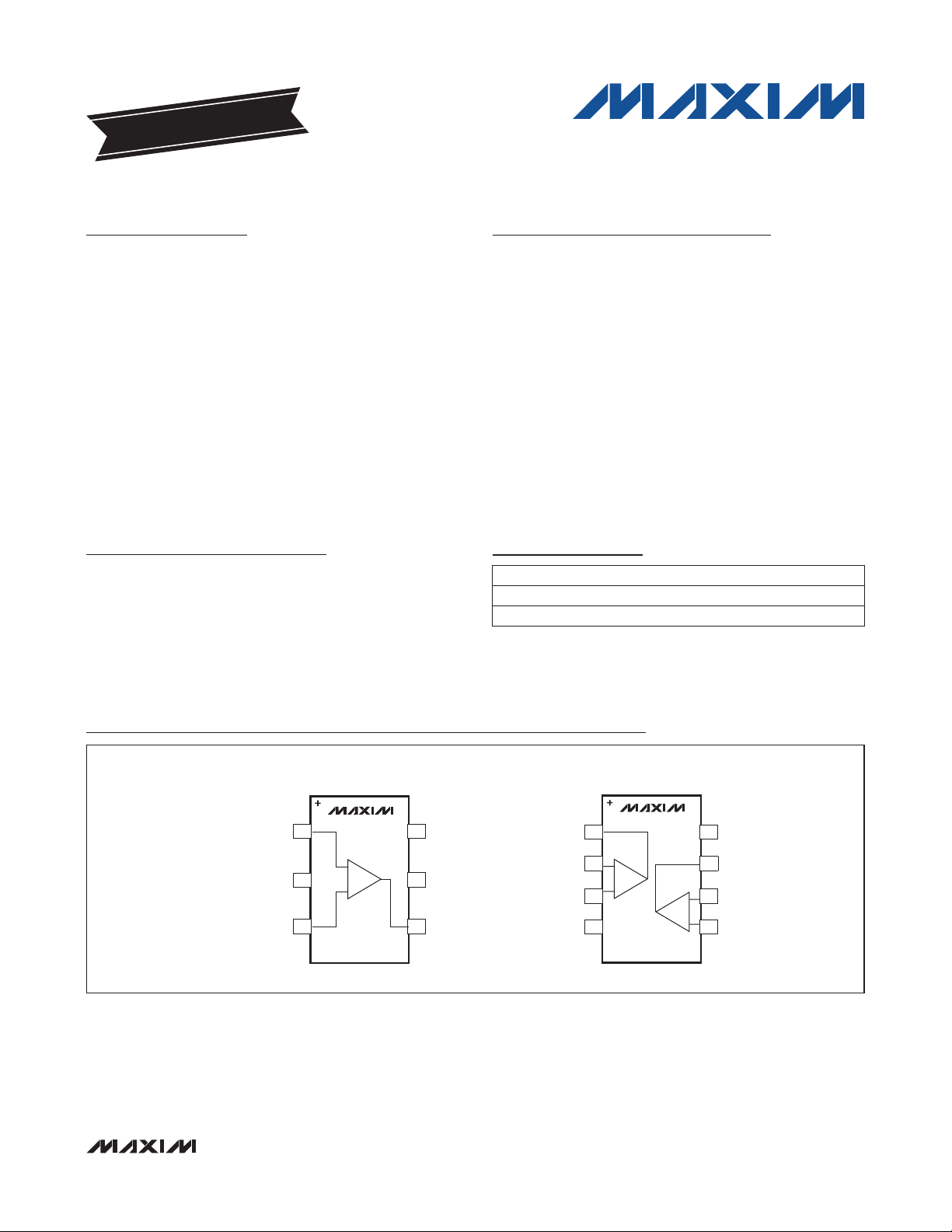
Functional Diagrams
TOP VIEW
IN+
GND
MAX9617
1
2
IN-
3
+
-
V
6
DD
5
V
DD
4
OUT
OUTA
INA-
INA+
GND
MAX9618
1
-
2
+
3
4
V
8
DD
7
OUTB
INB-
6
-
+
5
INB+
_______________________________________________________________ Maxim Integrated Products 1
For pricing, delivery, and ordering information, please contact Maxim Direct at 1-888-629-4642,
or visit Maxim’s website at www.maxim-ic.com.
Page 2
High-Efficiency, 1.5MHz
Op Amps with RRIO
ABSOLUTE MAXIMUM RATINGS
Supply Voltage (VDD to GND) .................................-0.3V to +6V
All Other Pins, IN+ to IN- .............(GND - 0.3V) to (VDD + 0.3V)
Short-Circuit Duration to Either Supply Rail,
OUT, OUTA, OUTB ............................................................ 10s
Continuous Input Current (any pins) ............................... ±20mA
Stresses beyond those listed under “Absolute Maximum Ratings” may cause permanent damage to the device. These are stress ratings only, and functional
operation of the device at these or any other conditions beyond those indicated in the operational sections of the specifications is not implied. Exposure to absolute
maximum rating conditions for extended periods may affect device reliability.
ELECTRICAL CHARACTERISTICS
(VDD = +3.3V, V
are at +25NC.) (Note 1)
PARAMETER SYMBOL CONDITIONS MIN TYP MAX UNITS
POWER SUPPLY
MAX9617/MAX9618
Supply Voltage Range V
Supply Current
(per Amplifier)
Power-Supply Rejection Ratio
(Note 2)
Power-Up Time t
DC SPECIFICATIONS
Input Offset Voltage (Note 2) V
Input Offset Voltage Drift
(Note 2)
Input Bias Current (Note 2) I
Input Offset Current I
Input Common-Mode Range V
Common-Mode Rejection Ratio
(Note 2)
Open-Loop Gain (Note 2) AV
GND
= 0V, V
IN+
= V
= VDD/2, RL = 100kI to VDD/2, TA = -40NC to +125NC, unless otherwise noted. Typical values
IN-
Guaranteed by PSRR, 0NC P TA P +70NC
DD
Guaranteed by PSRR, -40NC P TA P +125NC
I
DD
PSRR
ON
DV
OS
CMRR
TA = +25NC
-40NC P TA P +125NC
VDD = 1.8V to 5.5V
0NC P TA P +70NC, VDD = 1.6V to 5.5V
VDD = 0 to 3V step, AV = 1V/V 20
OS
CM
TA = +25NC
-40NC P TA P +125NC
OS
TA =+25NC
B
-40NC P TA P +125NC
Guaranteed by
CMRR test
-0.1V P VCM P VDD + 0.1V, TA = +25NC
-0.1V P VCM P VDD + 0.05V,
-40NC P TA P +125NC
20mV P V
RL = 100kI to VDD/2
OL
150mV P V
RL = 5kI to VDD/2
OUT
OUT
Continuous Power Dissipation (TA = +70NC)
6-Pin SC70 (derate 3.1mW/NC above +70NC) ..........245.4mW
8-Pin SC70 (derate 3.1mW/NC above +70NC) .............245mW
Operating Temperature Range ........................ -40NC to +125NC
Junction Temperature .....................................................+150NC
Storage Temperature Range ............................ -65NC to +150NC
Lead Temperature (soldering, 10s) ................................+300NC
1.6 5.5
1.8 5.5
59 78
111
TA = +25NC
-40NC P TA P +125NC
TA = +25NC
-40NC P TA P +125NC
P VDD - 20mV,
P VDD - 150mV,
119 135
107
116 135
0.8 10
5 120
0.01 0.14
0.005
-0.1
-0.1
122 135
116
120 138
123 160
25
3.5
VDD +
0.1
VDD +
0.05
V
FA
dB
Fs
FV
nV/NC
nA
V
dB
dB
2 ______________________________________________________________________________________
Page 3
High-Efficiency, 1.5MHz
Op Amps with RRIO
ELECTRICAL CHARACTERISTICS (continued)
(VDD = +3.3V, V
are at +25NC.) (Note 1)
PARAMETER SYMBOL CONDITIONS MIN TYP MAX UNITS
Input Resistance R
Output-Voltage Swing
Short-Circuit Current I
AC SPECIFICATIONS
Gain-Bandwidth Product GBWP 1.5 MHz
Slew Rate SR
Input Voltage-Noise Density e
Input Voltage Noise
Input Current-Noise Density i
Phase Margin CL = 20pF 60 Degrees
Capacitive Loading C
Crosstalk f = 10kHz (MAX9618) -100 dB
Note 1: Specifications are 100% tested at TA = +25NC (exceptions noted). All temperature limits are guaranteed by design.
Note 2: Guaranteed by design.
GND
= 0V, V
IN+
= V
= VDD/2, RL = 100kI to VDD/2, TA = -40NC to +125NC, unless otherwise noted. Typical values
IN-
Differential 50
IN
Common mode 200
RL = 100kI to VDD/2
V
OH
VDD - V
OUT
RL = 5kI to VDD/2
RL = 600I to VDD/2
50
RL = 100kI to VDD/2
V
OL
SC
V
OUT
RL = 5kI to VDD/2
RL = 600I to VDD/2
50
150 mA
0V P V
f = 1kHz 42
n
OUT
P 2V
0.1Hz P f P 10Hz
f = 1kHz 100
n
No sustained oscillation, AV = 1V/V 400 pF
L
0.7
1
12
22
11
18
MI
mV
V/Fs
nV/√Hz
FV
P-P
fA/√Hz
MAX9617/MAX9618
Typical Operating Characteristics
(VDD = +3.3V, V
= 0V, outputs have RL = 100kI connected to VDD/2. TA = +25NC, unless otherwise specified.)
GND
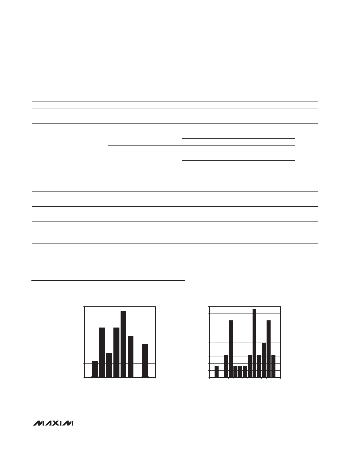
INPUT OFFSET VOLTAGE
DRIFT HISTOGRAM
-0.03
OFFSET VOLTAGE DRIFT (FV/NC)
MAX9617 toc02
0.01 0.02 0.03 0.04-0.02 -0.01 0
25
20
15
10
FREQUENCY (%)
5
0
0
OFFSET VOLTAGE HISTOGRAM
OFFSET VOLTAGE (FV)
20
MAX9617 toc01
4321
18
16
14
12
10
8
FREQUENCY (%)
6
4
2
0
_______________________________________________________________________________________ 3
Page 4

High-Efficiency, 1.5MHz
Op Amps with RRIO
Typical Operating Characteristics (continued)
(VDD = +3.3V, V
= 0V, outputs have RL = 100kI connected to VDD/2. TA = +25NC, unless otherwise specified.)
GND
SUPPLY CURRENT
vs. SUPPLY VOLTAGE
120
100
80
60
40
SUPPLY CURRENT (FA)
20
MAX9617/MAX9618
0
1.6 5.6
TA = +125NC
TA = +25NC
TA = -40NC
SUPPLY VOLTAGE (V)
MAX9617 toc03
SUPPLY CURRENT (FA)
5.14.64.13.63.12.62.1
INPUT OFFSET VOLTAGE
vs. TEMPERATURE
6
5
4
(FV)
3
OS
V
2
1
0
-50 125
TEMPERATURE (NC)
MAX9617 toc06
INPUT BIAS CURRENT (pA)
1007550250-25
COMMON-MODE REJECTION RATIO
vs. TEMPERATURE
140
120
100
CMRR (dB)
80
60
40
-50 125
TEMPERATURE (NC)
MAX9617 toc09
PSRR (dB)
1007550250-25
SUPPLY CURRENT
vs. TEMPERATURE
100
90
80
70
60
50
40
30
20
10
0
-50 125
TEMPERATURE (NC)
INPUT BIAS CURRENT
vs. INPUT COMMON MODE
300
250
200
150
100
50
0
-0.1 3.4
NONINVERTING INPUT
INVERTING INPUT
INPUT COMMON MODE (V)
POWER-SUPPLY REJECTION RATIO
vs. FREQUENCY
140
120
100
80
60
40
20
0
0.1 10M
FREQUENCY (Hz)
INPUT OFFSET VOLTAGE
vs. INPUT COMMON MODE
6
MAX9617 toc04
1007525 500-25
5
4
(FV)
3
OS
V
TA = +25NC
2
1
0
-0.1 3.4
TA = -40NC
INPUT COMMON MODE (V)
T
A
= +125NC
MAX9617 toc05
2.92.41.91.40.90.4
COMMON-MODE REJECTION RATIO
vs. FREQUENCY
140
120
MAX9617 toc07
100
80
60
CMRR (dB)
40
20
2.92.41.91.40.90.4
0
0.1 10M
FREQUENCY (Hz)
MAX9617 toc08
1M100k10k1k100101
OUTPUT-VOLTAGE SWING HIGH
vs. TEMPERATURE
0.40
0.38
MAX9617 toc10
0.36
0.34
0.32
(mV)
0.30
OH
V
0.28
0.26
0.24
0.22
0.20
1M100k10k1k100101
-50 125
TEMPERATURE (NC)
MAX9617 toc11
1007525 500-25
4 ______________________________________________________________________________________
Page 5

High-Efficiency, 1.5MHz
Op Amps with RRIO
Typical Operating Characteristics (continued)
(VDD = +3.3V, V
= 0V, outputs have RL = 100kI connected to VDD/2. TA = +25NC, unless otherwise specified.)
GND
MAX9617/MAX9618
OUTPUT-VOLTAGE SWING LOW
vs. TEMPERATURE
0.40
0.38
0.36
0.34
0.32
(mV)
0.30
OL
V
0.28
0.26
0.24
0.22
0.20
-50 125
TEMPERATURE (NC)
INPUT VOLTAGE 0.1Hz TO 10Hz NOISE
OPEN-LOOP GAIN vs. FREQUENCY
160
140
MAX9617 toc12
120
100
80
60
40
OPEN LOOP GAIN (dB)
20
0
-20
1007525 500-25
-40
-10m 1M 10M
FREQUENCY (Hz)
100k10k100 1k1 10100m
MAX9617 toc13
INPUT VOLTAGE NOISE vs. FREQUENCY
10,000
1000
100
INPUT VOLTAGE NOISE (nV/√Hz)
10
0.1 100k
FREQUENCY (Hz)
MAX9617 toc14
10k1k100101
INPUT CURRENT NOISE
MAX9617 toc15
0.1FV/div
1000
100
vs. FREQUENCY
MAX9617 toc16
SMALL-SIGNAL GAIN
vs. FREQUENCY
5
0
-5
-10
-15
-20
SMALL-SIGNAL GAIN (dB)
-25
-30
-35
10 10M
FREQUENCY (kHz)
_______________________________________________________________________________________ 5
1s/div
100mV
1M100k100 1k 10k
INPUT CURRENT NOISE (fA/√Hz)
10
LARGE-SIGNAL GAIN
vs. FREQUENCY
P-P
10
MAX9617 toc17
0
-10
-20
-30
LARGE-SIGNAL GAIN (dB)
-40
-50
10 10M
FREQUENCY (kHz)
1 10 100 1k
0.1 10k
FREQUENCY (Hz)
SMALL-SIGNAL STEP RESPONSE
vs. TIME
2V
P-P
MAX9617 toc18
1M100k10k1k100
100Fs/div
MAX9617 toc19
100mV
P-P
50mV/div
Page 6

High-Efficiency, 1.5MHz
Op Amps with RRIO
Typical Operating Characteristics (continued)
(VDD = +3.3V, V
= 0V, outputs have RL = 100kI connected to VDD/2. TA = +25NC, unless otherwise specified.)
GND
LARGE-SIGNAL STEP RESPONSE
vs. TIME
MAX9617 toc20
100mV
P-P
10,000
CAPACITIVE LOAD
vs. ISOLATION RESISTOR
VIN = 100mV
AV = 1V/V
P-P
MAX9617 toc21
500mV/div
100Fs/div
MAX9617/MAX9618
1000
UNSTABLE
CAPACITENCE (pF)
100
0.1 1000
ISOLATION RESISTOR (I)
100101
Pin Configurations
TOP VIEW
IN+
GND
+
1
2
MAX9617
IN-
3
V
6
DD
V
5
DD
4
OUT
OUTA
SC70
INA-
INA+
GND
+
1
2
MAX9618
3
4
V
8
DD
7
OUTB
INB-
6
5
INB+
SC70
Pin Description
PIN
MAX9617 MAX9618
NAME FUNCTION
1 — IN+ Positive Input
2 4 GND Ground
3 — IN- Negative Input
4 — OUT Output
5, 6 8 V
DD
Positive Supply Voltage. Bypass to GND with a 0.1FF capacitor.
— 1 OUTA Channel A Output
— 2 INA- Channel A Negative Input
— 3 INA+ Channel A Positive Input
— 5 INB+ Channel B Positive Input
— 6 INB- Channel B Negative Input
— 7 OUTB Channel B Output
6 ______________________________________________________________________________________
Page 7
High-Efficiency, 1.5MHz
Op Amps with RRIO
MAX9617/MAX9618
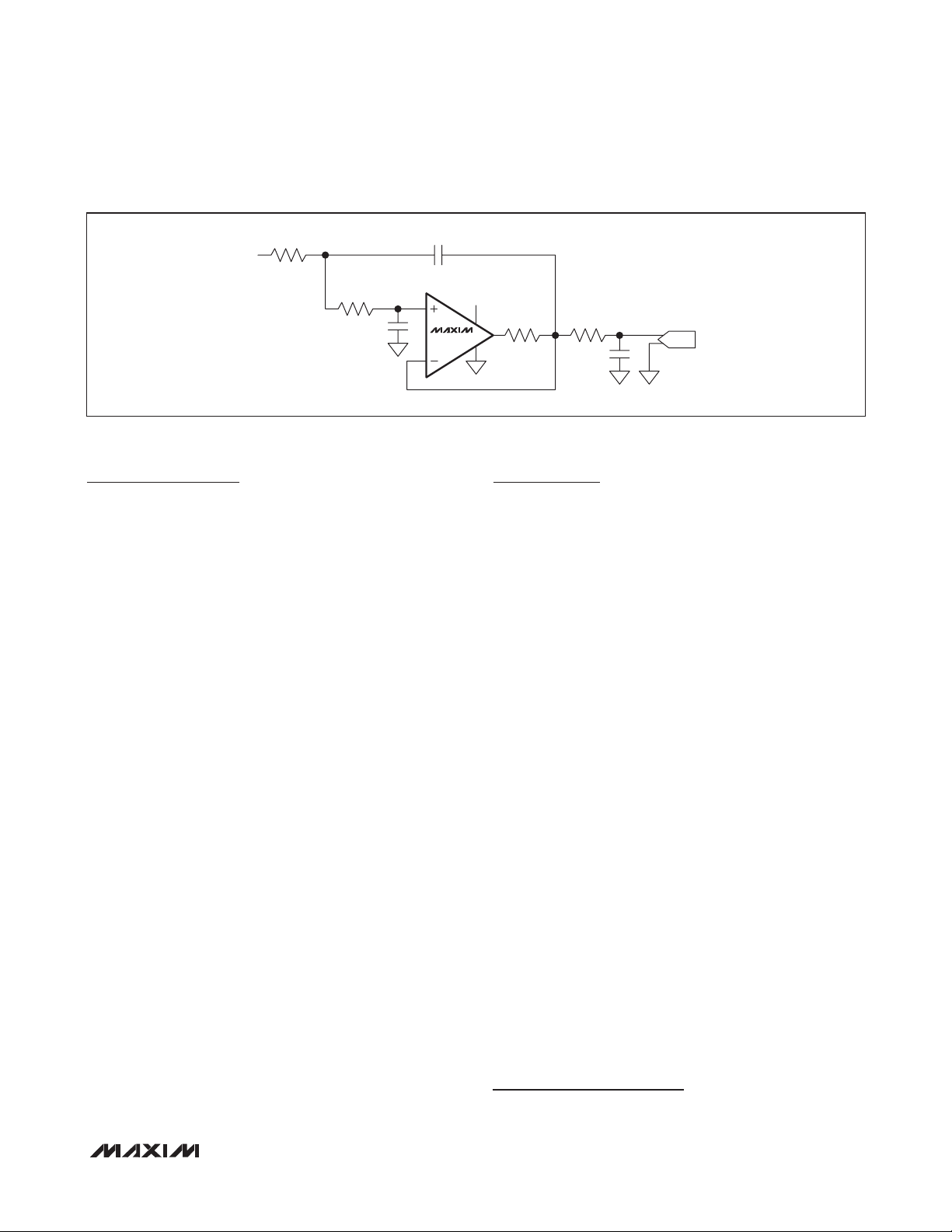
V
IN
+5V
MAX9617
Figure 1. Typical Application Circuit: Sallen-Key Active Lowpass Filter
Detailed Description
The MAX9617 (single) and MAX9618 (dual) are precision, low-power op amps ideal for signal processing
applications. These devices use an innovative autozero
technique that allows precision and low noise with a
minimum amount of power. The low input offset voltage,
CMOS inputs, and the absence of 1/f noise allows for
optimization of active filter designs.
The MAX9617/MAX9618 achieve rail-to-rail performance
at the input through the use of a low-noise charge pump.
This ensures a glitch-free, common-mode input voltage
range extending from the negative supply rail up to
the positive supply rail, eliminating crossover distortion
common to traditional n-channel/p-channel CMOS pair
inputs, reducing harmonic distortion at the output.
Autozero
The MAX9617/MAX9618 feature an autozero circuit that
allows the device to achieve less than 10FV (max) of
input offset voltage and eliminates the 1/f noise.
Internal Charge Pump
An internal charge pump provides an internal supply typically 1V beyond the upper rail. This internal rail allows the
MAX9617/MAX9618 to achieve true rail-to-rail inputs and
outputs, while providing excellent common-mode rejection, power-supply rejection ratios, and gain linearity.
The charge pump requires no external components, and
in most applications is entirely transparent to the user.
The operating frequency is well beyond the unity-gain
frequency of the amplifier, avoiding aliasing or other signal integrity issues in sensitive applications.
ADC
Applications Information
The MAX9617/MAX9618 low-power, low-noise, and precision operational amplifiers are designed for applications in the portable medical, such as ECG and pulse
oximetry, portable consumer, and industrial markets.
The MAX9617/MAX9618 are also ideal for loop-powered
systems that interface with pressure sensors or strain
gauges.
Capacitive-Load Stability
Driving large capacitive loads can cause instability in
many op amps. The MAX9617/MAX9618 are stable
with capacitive loads up to 400pF. Stability with higher
capacitive loads can be improved by adding an isolation
resistor in series with the op-amp output. This resistor
improves the circuit’s phase margin by isolating the load
capacitor from the amplifier’s output. The graph in the
Typical Operating Characteristics gives the stable operation region for capacitive load versus isolation resistors.
Power Supplies and Layout
The MAX9617/MAX9618 operate either with a single supply from +1.6V to +5.5V with respect to ground or with
dual supplies from Q0.8V to Q2.75V. When used with
dual supplies, bypass both supplies with their own 0.1FF
capacitor to ground. When used with a single supply,
bypass VDD with a 0.1FF capacitor to ground.
Careful layout technique helps optimize performance by
decreasing the amount of stray capacitance at the op
amp’s inputs and outputs. To decrease stray capacitance, minimize trace lengths by placing external components close to the op amp’s pins.
Chip Information
PROCESS: BiCMOS
_______________________________________________________________________________________ 7
Page 8
High-Efficiency, 1.5MHz
Op Amps with RRIO
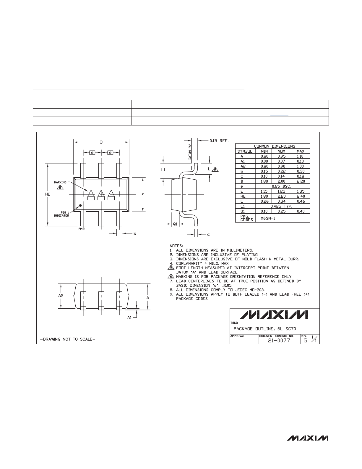
Package Information
For the latest package outline information and land patterns, go to www.maxim-ic.com/packages.
PACKAGE TYPE PACKAGE CODE DOCUMENT NO.
6 SC70 X6SN-1
8 SC70 X8C+1
21-0077
21-0460
MAX9617/MAX9618
SC70, 6L.EPS
8 ______________________________________________________________________________________
Page 9

High-Efficiency, 1.5MHz
Op Amps with RRIO
Package Information (continued)
For the latest package outline information and land patterns, go to www.maxim-ic.com/packages.
MAX9617/MAX9618
_______________________________________________________________________________________ 9
Page 10

High-Efficiency, 1.5MHz
Op Amps with RRIO
Revision History
REVISION
NUMBER
0 7/09 Initial release —
1 9/09 Removed references to MAX9617 shutdown functionality 1, 2, 3, 6, 7
REVISION
DATE
MAX9617/MAX9618
DESCRIPTION
PAGES
CHANGED
Maxim cannot assume responsibility for use of any circuitry other than circuitry entirely embodied in a Maxim product. No circuit patent licenses are implied.
Maxim reserves the right to change the circuitry and specifications without notice at any time.
10 Maxim Integrated Products, 120 San Gabriel Drive, Sunnyvale, CA 94086 408-737-7600
©
2009 Maxim Integrated Products Maxim is a registered trademark of Maxim Integrated Products, Inc.
 Loading...