

Page 1
General Description
The MAX9610 high-side current-sense amplifier offers
precision accuracy specifications of VOSless than
500μV (max) and gain error less than 0.5% (max). This
device features an ultra-low 1μA quiescent supply current. The MAX9610 fits in a tiny, 1mm x 1.5mm μDFN
package or a 5-pin SC70 package, making this part
ideal for applications in notebook computers, cell
phones, cameras, PDAs, and all lithium-ion batteryoperated portable devices where accuracy, low quiescent current, and small size are critical.
The MAX9610 features an input voltage range (common mode) from 1.6V to 5.5V. This input range is excellent for monitoring the current of a single-cell,
lithium-ion battery (Li+), which at full charge is 4.2V,
typically 3.6V in normal use, and less than 2.9V when
ready to be recharged. These current-sense amplifiers
have a voltage output and are offered in three gain versions: 25V/V (MAX9610T), 50V/V (MAX9610F), and
100V/V (MAX9610H).
The three gain versions offer flexibility in the choice of
the external current-sense resistor. The very low 500μV
(max) input offset voltage allows small 25mV to 50mV
full-scale V
SENSE
voltage for very low voltage drop at
full-load current measurement.
The MAX9610 is offered in tiny 6-pin μDFN, (1mm x
1.5mm x 0.8mm footprint) and 5-pin SC70 packages,
specified for operation over the -40°C to +85°C temperature range.
For a very similar 1.6V to 28V input voltage device in a
4-bump UCSP™ package (1mm x 1mm x 0.6mm), refer
to the MAX9938 data sheet.
Applications
Cell Phones
Cameras
Portable Li+ Battery Powered Systems
3.3V and 5V Power Management Systems
PDAs
USB Ports
Features
♦ Ultra-Low Supply Current of 1µA (max)
♦ Low 500µV (max) Input Offset Voltage
♦ Low < 0.5% (max) Gain Error
♦ Input Common Mode: +1.6V to +5.5V
♦ Voltage Output
♦ Three Gain Versions Available
25V/V (MAX9610T)
50V/V (MAX9610F)
100V/V (MAX9610H)
♦ Tiny µDFN (1mm x 1.5mm x 0.8mm) and
SC70 Packages
MAX9610
1µA, µDFN/SC70, Lithium-Ion Battery,
Precision Current-Sense Amplifier
________________________________________________________________
Maxim Integrated Products
1
19-4342; Rev 0; 10/08
For pricing, delivery, and ordering information, please contact Maxim Direct at 1-888-629-4642,
or visit Maxim’s website at www.maxim-ic.com.
Pin Configurations appear at end of data sheet.
UCSP is a trademark of Maxim Integrated Products, Inc.
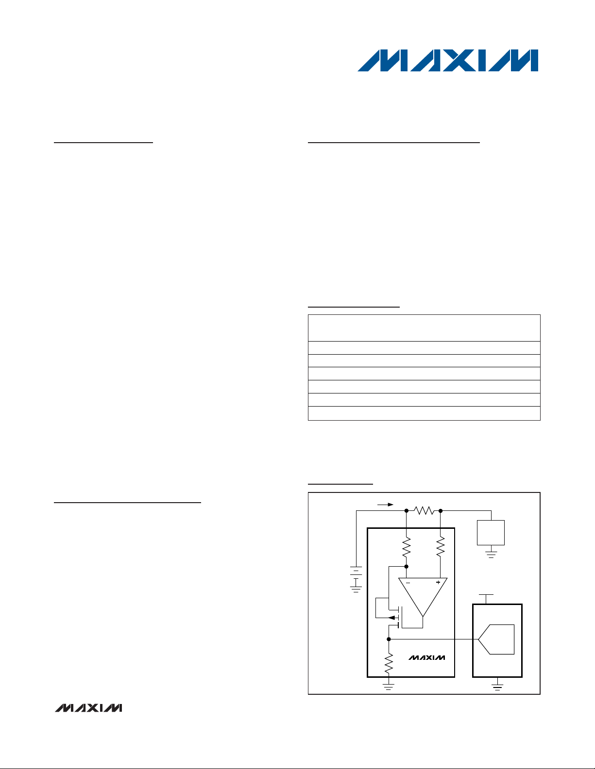
MAX9610
P
R
OUT
10kΩ
GND
OUT
ADC
μC
LOAD
V
DD
= 3.3V
RS-
RS+
R
SENSE
I
LOAD
V
BATT
=
1.6V to 5.5V
R
1
R
1
Typical Operating Circuit
Ordering Information
PART*
PIN-
GAIN
(V/V)
TOP MARK
MAX9610TELT+T 6 μDFN 25 OU
MAX9610FELT+T 6 μDFN 50 OS
MAX9610HELT+T 6 μDFN 100 OT
MAX9610TEXK+T 5 SC70 25 ATG
MAX9610FEXK+T 5 SC70 50 ATE
MAX9610HEXK+T 5 SC70 100 ATF
*
All devices are specified over the -40°C to +85°C extended
temperature range.
+
Denotes a lead-free/RoHS-compliant package.
T = Tape and reel.
PACKAGE
Page 2
MAX9610
1µA, µDFN/SC70, Lithium-Ion Battery,
Precision Current-Sense Amplifier
2 _______________________________________________________________________________________
ABSOLUTE MAXIMUM RATINGS
ELECTRICAL CHARACTERISTICS
(V
RS+
= V
RS-
= 3.6V, V
SENSE
= (V
RS+
- V
RS-
) = 0, TA= -40°C to +85°C, unless otherwise noted. Typical values are at TA= +25°C.)
(Note 1)
Stresses beyond those listed under “Absolute Maximum Ratings” may cause permanent damage to the device. These are stress ratings only, and functional
operation of the device at these or any other conditions beyond those indicated in the operational sections of the specifications is not implied. Exposure to
absolute maximum rating conditions for extended periods may affect device reliability.
RS+, RS- to GND......................................................-0.3V to +6V
OUT to GND .............................................................-0.3V to +6V
RS+ to RS- .............................................................................±6V
Short-Circuit Duration: OUT to GND or RS+ ..............Continuous
Continuous Input Current (Any Pin)..................................±20mA
Continuous Power Dissipation (T
A
= +70°C)
5-Pin SC70 (derate 3.1mW/°C above +70°C)..............247mW
6-Pin μDFN (derate 2.1mW/°C above +70°C) .............168mW
Operating Temperature Range ...........................-40°C to +85°C
Junction Temperature......................................................+150°C
Storage Temperature Range .............................-65°C to +150°C
Lead Temperature (soldering, 10s) .................................+300°C
Package Reflow Soldering Temperature .........................+260°C
PARAMETER
CONDITIONS
UNITS
V
RS+
= 3.6V, TA = +25°C 0.6 1.0
V
RS+
= 3.6V, -40°C < TA < +85°C 1.4
V
RS+
= 5.5V, TA = +25°C
1.2
Supply Current
(Note 2)
I
CC
V
RS+
= 5.5V, -40°C < TA < +85°C 1.6
μA
Common-Mode Input Range V
CM
Guaranteed by CMRR,
-40°C < T
A
< +85°C
1.6 5.5 V
Common-Mode Rejection Ratio CMRR
80
dB
TA = +25°C, gain = 25, 50, 100 (Note 3)
Gain = 25, 50
Input Offset Voltage V
OS
Gain = 100
μV
MAX9610T 25
MAX9610F 50Gain G
MAX9610H
V/V
TA = +25°C, gain = 25, 50, 100 (Note 4)
Gain = 25, 50
Gain Error GE
Gain = 100 ±1
%
Output Resistance R
OUT
TA = +25°C (Note 5) 7.0 10
kΩ
G = 25 2.5 15
G = 50 5 30
OUT Low Voltage V
OL
G = 100 10 70
mV
OUT High Voltage V
OH
VOH = V
RS-
- V
OUT
(Note 6) 0.1 0.2 V
SYMBOL
MIN TYP MAX
0.75
1.6V < V
-40°C < TA < +85°C
-40°C < TA < +85°C
< 5.5V, -40°C < TA < +85°C
RS+
104
±100 ±500
±600
±700
100
±0.1 ±0.5
±0.8
13.2
Page 3
MAX9610
1µA, µDFN/SC70, Lithium-Ion Battery,
Precision Current-Sense Amplifier
_______________________________________________________________________________________ 3
PARAMETER
SYMBOL
CONDITIONS
MIN
TYP
MAX
UNITS
V
SENSE
= 50mV, G = 25
V
SENSE
= 50mV, G = 50
Small-Signal Bandwidth BW
V
SENSE
= 50mV, G = 100 60
kHz
Output Settling Time t
S
1% final value, V
SENSE
= 25mV 35 μs
Power-Up Time t
ON
1% final value, V
SENSE
= 25mV
μs
ELECTRICAL CHARACTERISTICS (continued)
(V
RS+
= V
RS-
= 3.6V, V
SENSE
= (V
RS+
- V
RS-
) = 0, TA= -40°C to +85°C, unless otherwise noted. Typical values are at TA= +25°C.)
(Note 1)
Note 1: All devices are 100% production tested at T
A
= +25°C. All temperature limits are guaranteed by design.
Note 2: V
OUT
= 0V. ICCis the total current into RS+ plus RS-.
Note 3: V
OS
is extrapolated from measurements for the Gain Error test.
Note 4: Gain Error is calculated by applying two values of V
SENSE
and calculating the error of the slope, vs. the ideal:
G = 25: V
SENSE
20mV and 120mV
G = 50: V
SENSE
10mV and 60mV
G = 100: V
SENSE
5mV and 30mV
Note 5: The device is stable for any external capacitance value.
Note 6: V
OH
is the voltage from V
RS-
to V
OUT
with V
SENSE
= 3.6V/Gain.
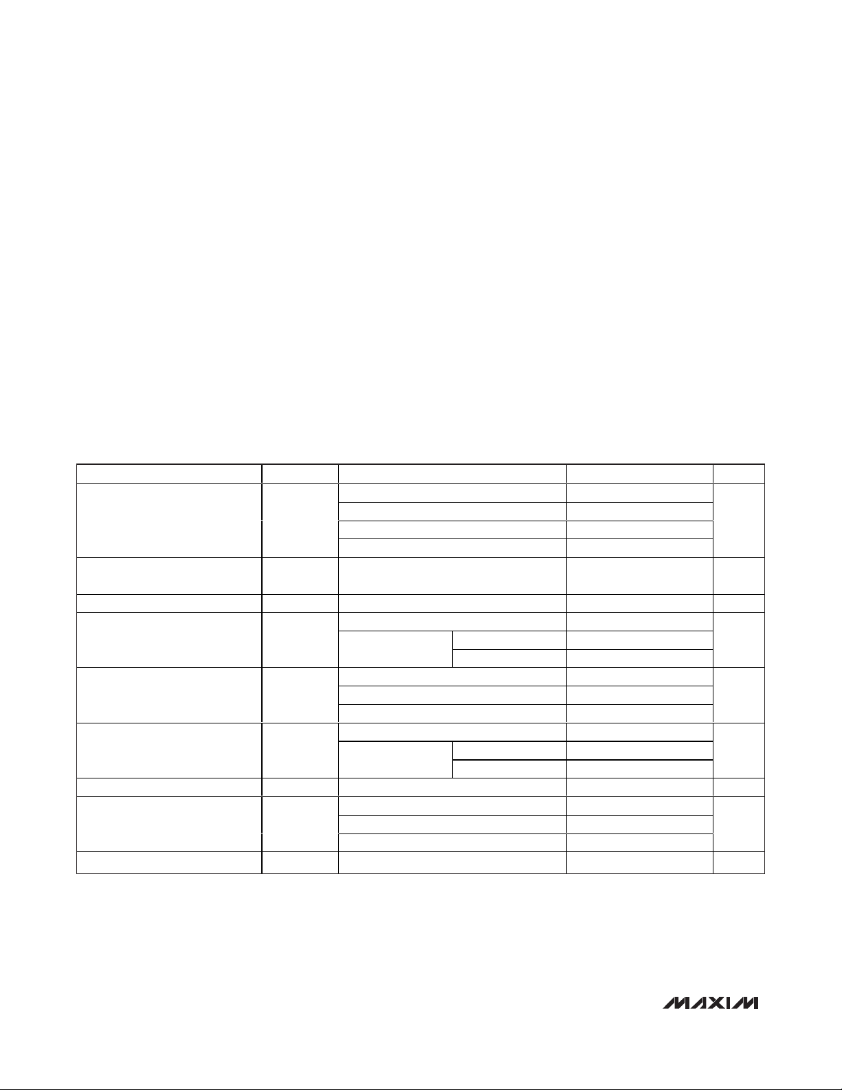
Typical Operating Characteristics
(V
RS+
= V
RS-
= 3.6V, TA= +25°C.)
20
15
10
5
0
-250
-200-150 -100 -50 0
25020015010050
MAX9610F
OFFSET VOLTAGE HISTOGRAM
MAX9610 toc01
OFFSET VOLTAGE (μV)
N (%)
30
25
20
15
10
5
0
-0.2
-0.15 -0.1 -0.05 0
0.20.150.10.05
MAX9610F
GAIN ACCURACY HISTOGRAM
MAX9610 toc02
GAIN ACCURACY (%)
N (%)
0
300
200
100
400
500
600
700
800
900
1000
-40 10-15 35 60 85
SUPPLY CURRENT
vs. TEMPERATURE
MAX9610 toc03
TEMPERATURE (°C)
SUPPLY CURRENT (nA)
5.5V
3.6V
1.6V
170
110
100
Page 4
MAX9610
1µA, µDFN/SC70, Lithium-Ion Battery,
Precision Current-Sense Amplifier
4 _______________________________________________________________________________________
Typical Operating Characteristics (continued)
(V
RS+
= V
RS-
= 3.6V, TA= +25°C.)
SUPPLY CURRENT
vs. COMMON-MODE VOLTAGE
MAX9610 toc04
COMMON-MODE VOLTAGE (V)
SUPPLY CURRENT (μA)
4.64.13.1 3.62.62.1
0.10
0.20
0.30
0.40
0.50
0.60
0.70
0.80
0.90
1.00
0
1.6 5.5
0
30
20
10
40
50
60
70
80
90
100
-40 10-15 35 60 85
OFFSET VOLTAGE
vs. TEMPERATURE
MAX9610 toc05
TEMPERATURE (°C)
OFFSET VOLTAGE (μV)
0
10
20
30
40
50
60
1.6 2.62.1 3.1 3.6 4.1 4.6 5.1
5.5
OFFSET VOLTAGE
vs. COMMON-MODE VOLTAGE
MAX9610 toc06
COMMON-MODE VOLTAGE (V)
OFFSET VOLTAGE (μV)
GAIN ERROR vs. TEMPERATURE
MAX9610 toc07
TEMPERATURE (°C)
GAIN ERROR (%)
603510-15
0.07%
0.09%
0.11%
0.13%
0.15%
0.17%
0.19%
0.21%
0.23%
0.25%
0.05%
-40 85
-0.20%
-0.16%
-0.18%
-0.12%
-0.14%
-0.08%
-0.10%
-0.06%
-0.02%
-0.04%
0%
1.6 2.6 3.12.1 3.6 4.1 4.6 5.1 5.5
GAIN ERROR
vs. COMMON-MODE VOLTAGE
MAX9610 toc08
COMMON-MODE VOLTAGE (V)
GAIN ERROR (%)
V
OUT
vs. V
SENSE
V
RS+
= 5.5V
MAX9610 toc09
V
SENSE
(mV)
V
OUT
(V)
20015010050
0.5
1.0
1.5
2.0
2.5
3.0
3.5
4.0
4.5
5.0
5.5
6.0
0
0 250
G = 25
G = 50
G = 100
0
0.8
0.6
0.4
0.2
1.0
1.2
1.6
1.4
1.8
010 4020 6050 7030 80
V
OUT
vs. V
SENSE
V
RS+
= 1.6V
MAX9610 toc10
V
SENSE
(mV)
V
OUT
(V)
G = 25
G = 50
G = 100
NORMALIZED GAIN
vs. FREQUENCY
MAX9610 toc11
FREQUENCY (kHz)
NORMALIZED GAIN (dB)
100101
-20
-15
-10
-5
0
5
-25
0.1 1000
G = 25
G = 50
G = 100
CMRR vs. FREQUENCY
MAX9610 toc12
FREQUENCY (Hz)
CMRR (dB)
10k1k100
-120
-100
-80
-60
-40
-20
-140
10 100k
Page 5

MAX9610
1µA, µDFN/SC70, Lithium-Ion Battery,
Precision Current-Sense Amplifier
_______________________________________________________________________________________ 5
Typical Operating Characteristics (continued)
(V
RS+
= V
RS-
= 3.6V, TA= +25°C.)
10μs/div
LARGE-SIGNAL RESPONSE
G = 50
50mV/div
1V/div
MAX9610 toc17
V
SENSE
V
OUT
10μs/div
LARGE-SIGNAL RESPONSE
G = 100
20mV/div
1V/div
MAX9610 toc18
V
SENSE
V
OUT
10μs/div
SMALL-SIGNAL RESPONSE
G = 100
5mV/div
200mV/div
MAX9610 toc15
V
SENSE
V
OUT
10μs/div
LARGE-SIGNAL RESPONSE
G = 25
100mV/div
1V/div
MAX9610 toc16
V
SENSE
V
OUT
10μs/div
SMALL-SIGNAL RESPONSE
G = 25
20mV/div
200mV/div
MAX9610 toc13
V
SENSE
V
OUT
10μs/div
SMALL-SIGNAL RESPONSE
G = 50
10mV/div
200mV/div
MAX9610 toc14
V
SENSE
V
OUT
Page 6

MAX9610
1µA, µDFN/SC70, Lithium-Ion Battery,
Precision Current-Sense Amplifier
6 _______________________________________________________________________________________
Detailed Description
The MAX9610 family of unidirectional high-side, current-sense amplifiers features a 1.6V to 5.5V input common-mode range. The input range is excellent for
monitoring the current of a single-cell lithium-ion battery
(Li+), which at full charge is 4.2V, typically 3.6V in normal use, and less than 2.9V when ready to be
recharged. The MAX9610 is ideal for many batterypowered, handheld devices because it uses only 1μA
quiescent supply current to extend battery life. The
MAX9610 monitors current through a current-sense
resistor and amplifies the voltage across that resistor.
See the
Typical Operating Circuit
on page 1.
The MAX9610 is a unidirectional current-sense amplifier
that has a well-established history. An op amp is used
to force the current through an internal gain resistor at
RS+ that has a value of R1, such that its voltage drop
equals the voltage drop across an external sense resistor, R
SENSE
. There is an internal resistor at RS- with the
same value as R1to minimize offset voltage. The current through R1is sourced by a pFET. Its drain current
is the same as its source current that flows through a
second gain resistor, R
OUT
. This produces an output
voltage, V
OUT
, whose magnitude is I
LOAD
x R
SENSE
x
R
OUT/R1
. The gain accuracy is based on the matching
of the two gain resistors R1and R
OUT
(see Table 1).
Total gain = 25V/V for the MAX9610T, 50V/V for the
MAX9610F, and 100V/V for the MAX9610H.
Applications Information
Choosing the Sense Resistor
Choose R
SENSE
based on the following criteria.
Voltage Loss
A high R
SENSE
value causes the power-source voltage
to drop due to IR loss. For minimal voltage loss, use the
lowest R
SENSE
value.
OUT Swing vs. V
RS+
and V
SENSE
The MAX9610 is unique since the supply voltage is the
input common-mode voltage (the average voltage at
RS+ and RS-). There is no separate VCCsupply voltage
input. Therefore, the OUT voltage swing is limited by
the minimum voltage at RS+.
V
OUT(MAX)
= V
RS+(MAX)
- V
SENSE(MAX)
- V
OH
and
V
SENSE
full scale should be less than V
OUT
/gain at the
minimum RS+ voltage. For best performance with a
3.6V supply voltage, select R
SENSE
to provide approximately 120mV (gain of 25V/V), 60mV (gain of 50V/V), or
30mV (gain of 100V/V) of sense voltage for the fullscale current in each application. These can be
increased by use of a higher minimum input voltage.
Accuracy
In the linear region (V
OUT
< V
OUT(MAX)
), there are two
components to accuracy: input offset voltage (V
OS
) and
Gain Error (GE). The MAX9610 has VOS= 500μV (max)
and Gain Error of 0.5% (max). Use the following linear
equation to calculate total error.
V
OUT
= (Gain ± GE) x V
SENSE
± (Gain x VOS)
A high R
SENSE
value allows lower currents to be measured more accurately because offsets are less significant when the sense voltage is larger.
Efficiency and Power Dissipation
At high current levels, the I2R loss in R
SENSE
can be
significant. Take this into consideration when choosing
the resistor value and its power dissipation (wattage)
rating. Also, the sense resistor’s value might drift if it is
allowed to heat up excessively. The precision VOSof
the MAX9610 allows the use of small sense resistors to
reduce power dissipation and reduce hot spots.
R
V
GI
SENSE
OUT
LOAD
=
× (max)
Pin Description
PIN
µDFN
NAME
FUNCTION
1 1, 2 GND Ground
2, 5 — N.C.
No Connection. Not internally
connected.
3 3 OUT Output
4 4 RS-
Load-Side Connection to
External Sense Resistor
6 5 RS+
Power-Side Connection to
External Sense Resistor
GAIN (V/V)
R
OUT
(Ω)
100 100 10k
50 200 10k
25 400 10k
Table 1. MAX9610, Internal Gain Setting
Resistors (Typical Values)
SC70
R1 (Ω)
Page 7

MAX9610
1µA, µDFN/SC70, Lithium-Ion Battery,
Precision Current-Sense Amplifier
_______________________________________________________________________________________ 7
Kelvin Connections
Because of the high currents that flow through R
SENSE
,
take care to eliminate parasitic trace resistance from
causing errors in the sense voltage. Either use a four
terminal current-sense resistor or use Kelvin (force and
sense) PCB layout techniques.
Optional Output Filter Capacitor
When designing a system that uses a sample and hold
stage in the analog-to-digital converter, the sampling
capacitor momentarily loads OUT and causes a drop in
the output voltage. If sampling time is very short (less
than a microsecond), consider using a ceramic capacitor across OUT and GND to hold V
OUT
constant during
sampling. This also decreases the small-signal bandwidth of the current-sense amplifier and reduces noise
at OUT.
Typical Application Circuit
Bidirectional Application
Battery-powered systems may require a precise bidirectional current-sense amplifier to accurately monitor
the battery’s charge and discharge currents.
Measurements of the two separate outputs with respect
to GND yield an accurate measure of the charge and
discharge currents, respectively (Figure 1).
MAX9610
P
R
OUT
GND
OUTOUT
ADC
ADC
LOAD
RS-
RS+
R
SENSE
I
LOAD
V
BATT
= 1.6V TO 5.5V
MAX9610
P
R
OUT
GND
RS-
RS+
R
1
R
1
R
1
R
1
MICRO-
CONTROLLER
VDD = 3.3V
TO WALL-CUBE/
CHARGER
Figure 1. Bidirectional Application
Page 8

MAX9610
1µA, µDFN/SC70, Lithium-Ion Battery,
Precision Current-Sense Amplifier
8 _______________________________________________________________________________________
Chip Information
PROCESS: BiCMOS
123
654
RS+ RS-N.C.
GND OUTN.C.
MAX9610T/F/H
1mm x 1.5mm μDFN
TOP VIEW
(PINS ON BOTTOM)
GND
RS-
OUT
1
5
RS+
GND
MAX9610T/F/H
2mm x 2.2mm SC70
TOP VIEW
23
4
(DIAGRAMS NOT TO SCALE.)
+
+
Pin Configurations
Page 9

MAX9610
1µA, µDFN/SC70, Lithium-Ion Battery,
Precision Current-Sense Amplifier
_______________________________________________________________________________________ 9
Package Information
For the latest package outline information and land patterns, go to www.maxim-ic.com/packages.
PACKAGE TYPE PACKAGE CODE DOCUMENT NO.
6 μDFN L611+1
21-0147
5 SC70 X5+1
21-0076
L
TOP VIEW
D
E
SIDE VIEW
A1
A
A 0.65
COMMON DIMENSIONS
PIN 1
0.075x45
BOTTOM VIEW
L1
32
MIN.
1
e
6
5
b
4
SECTION A-A
b
L2
A A
NOM.
0.72 0.80
MAX.
0.00
A1
0.05
1.501.45D 1.55
1.000.95E 1.05
0.350.30L 0.40
--0.00
L1
0.08
--0.05L2 0.10
0.200.17b 0.23
0.50 BSC.e
AA
TOPMARK
2
1
-DRAWING NOT TO SCALE-
DOCUMENT CONTROL NO.APPROVAL
TITLE:
REV.
PACKAGE OUTLINE, 6L uDFN, 1.5x1.0x0.8mm
21-0147
2
1
E
3
PIN 1
MARK
4
5
L611-1, L611-2
Pkg.
Code
--
--
A2
0.20 --
A2
6L UDFN.EPS
Page 10
MAX9610
1µA, µDFN/SC70, Lithium-Ion Battery,
Precision Current-Sense Amplifier
10 ______________________________________________________________________________________
-DRAWING NOT TO SCALE-
DOCUMENT CONTROL NO.APPROVAL
TITLE:
REV.
PACKAGE OUTLINE, 6L uDFN, 1.5x1.0x0.8mm
21-0147
2
2
E
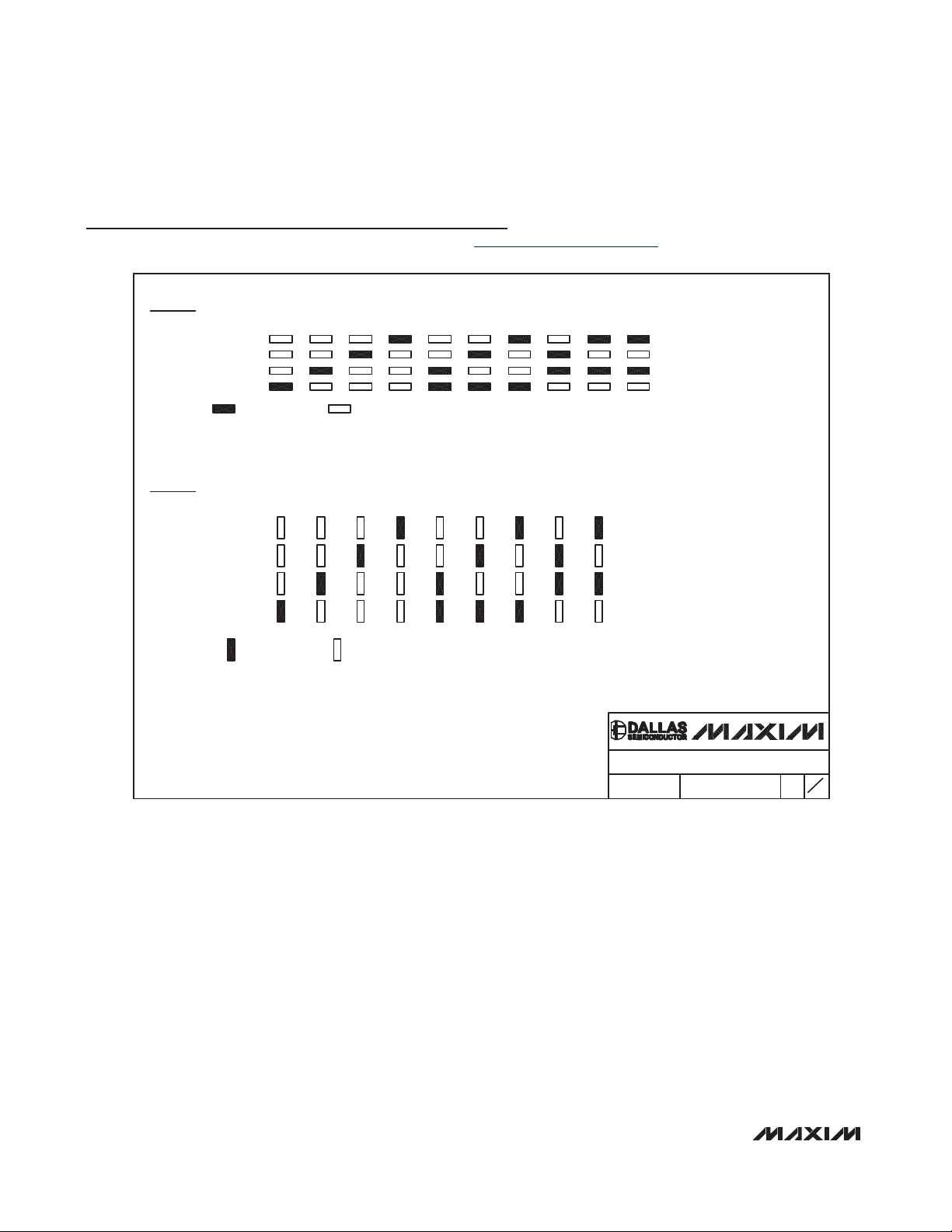
2005 2006 2007 2008 2009 2010 2011 2012 2013 2014Calendar Year
Legend:
Marked with bar Blank space - no bar required
06-11Payweek 12-17 18-23 24-29 30-35 36-41 42-47 48-51 52-05
TABLE 2 Translation Table for Payweek Binary Coding
TABLE 1 Translation Table for Calendar Year Code
Legend: Marked with bar Blank space - no bar required
Package Information (continued)
For the latest package outline information and land patterns, go to www.maxim-ic.com/packages.
Page 11

MAX9610
1µA, µDFN/SC70, Lithium-Ion Battery,
Precision Current-Sense Amplifier
Maxim cannot assume responsibility for use of any circuitry other than circuitry entirely embodied in a Maxim product. No circuit patent licenses are
implied. Maxim reserves the right to change the circuitry and specifications without notice at any time.
Maxim Integrated Products, 120 San Gabriel Drive, Sunnyvale, CA 94086 408-737-7600 ____________________
11
© 2008 Maxim Integrated Products is a registered trademark of Maxim Integrated Products, Inc.
SC70, 5L.EPS
PACKAGE OUTLINE, 5L SC70
21-0076
1
1
E
Package Information (continued)
For the latest package outline information and land patterns, go to www.maxim-ic.com/packages.
 Loading...