

Page 1
General Description
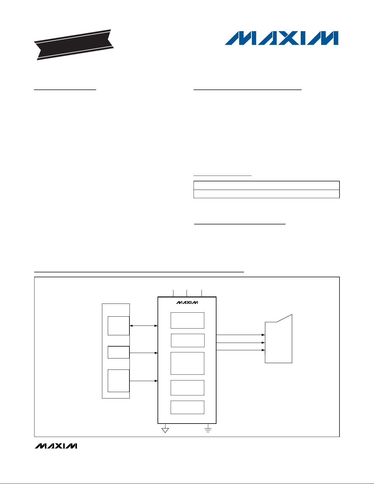
The MAX9597 single SCART interface routes audio and
video signals between a set-top box decoder chip and
an external SCART connector under I
2
C control.
Operating from a 3.3V supply and a 12V supply, the
MAX9597 consumes 53mW during quiescent operation
and 254mW during average operation when driving
typical signals into typical loads.
The MAX9597 audio section contains left and right audio
paths with an independent operational amplifier at the
inputs. The DirectDrive®output amplifiers create a
2V
RMS
full-scale audio signal biased around ground,
eliminating the need for bulky output capacitors and
reducing click-and-pop noise. The zero-cross detection
circuitry also further reduces clicks and pops by
enabling audio sources to switch only during a zerocrossing.
The MAX9597 video section contains 4 channels of
video filter amplifiers. The standard-definition video signals from the set-top box decoder chip are lowpass filtered to remove out-of-bandwidth artifacts. The
MAX9597 also supports slow-switching and fast-switching signals.
The MAX9597 is available in a compact 28-pin thin
QFN package and is specified over the 0°C to +70°C
commercial temperature range.
Features
♦ 53mW Quiescent Power Consumption
♦ 5µW Shutdown Consumption
♦ Audio Operational Amplifiers to Create Input
Filters
♦ Clickless/Popless, DirectDrive Audio
♦ Video Reconstruction Filter with 10MHz Passband
and 43dB Attenuation at 27MHz
♦ 3.3V and 12V Supply Voltages
MAX9597
Low-Power Audio/Video Interface
for Single SCART Connectors
________________________________________________________________
Maxim Integrated Products
1
19-4159; Rev 1; 10/08
For pricing, delivery, and ordering information, please contact Maxim Direct at 1-888-629-4642,
or visit Maxim’s website at www.maxim-ic.com.
EVALUATION KIT
AVAILABLE
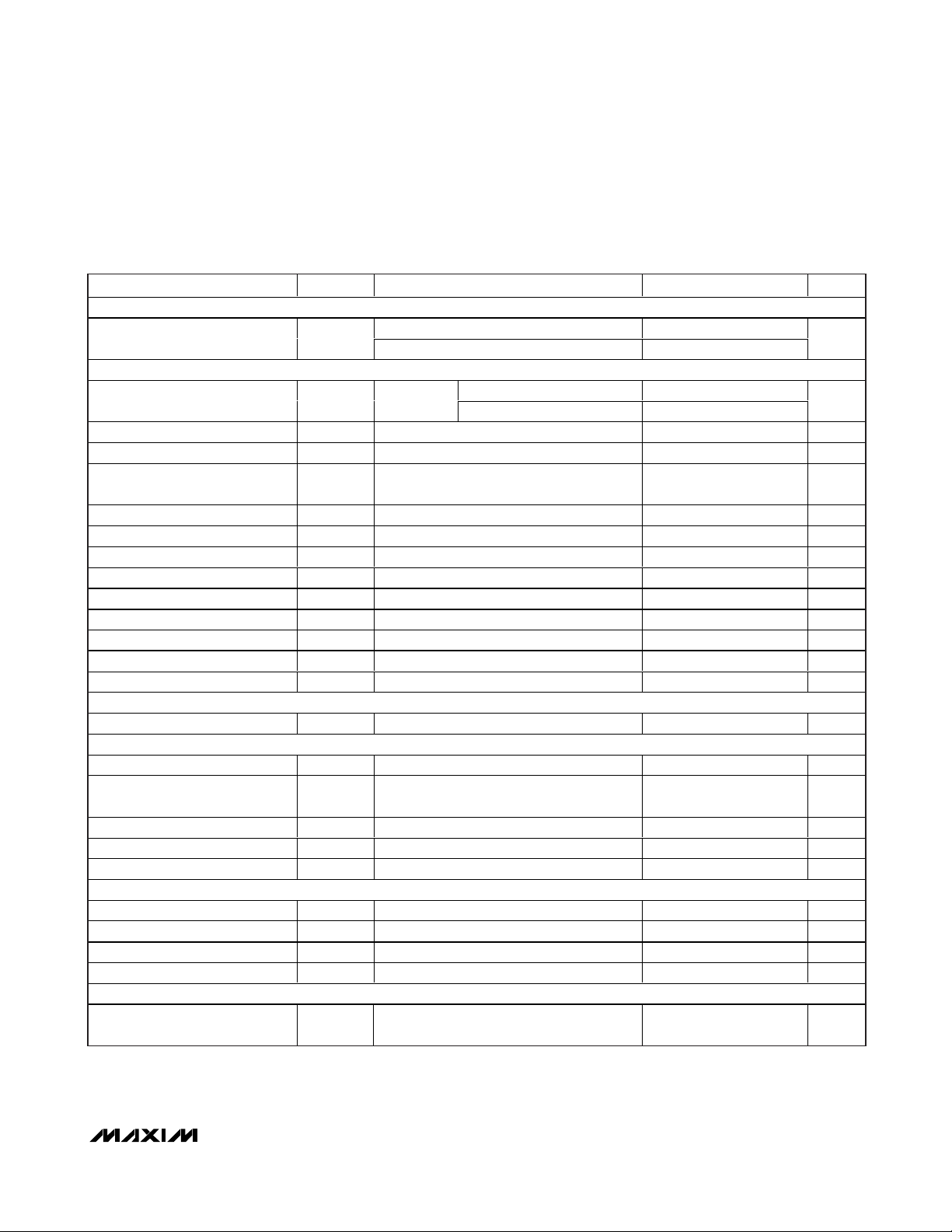
Ordering Information
+
Denotes a lead-free/RoHS-compliant package.
*
EP = Exposed pad.
PART TEMP RANGE PIN-PACKAGE
MAX9597CTI+ 0°C to +70°C 28 TQFN-EP*
I2C INTERFACE
AND REGISTERS
MAX9597
VIDEO FILTERS
AUDIO
WITH DirectDrive
OUTPUTS
SLOW SWITCHING
FAST SWITCHING
CHARGE PUMP
V
12
V
AUD
V
ID
12V 3.3V3.3V
EP
GND
μC
VIDEO
ENCODER
STEREO
AUDIO
DAC
RGB, Y/C, CVBS
SINGLE OR
DIFFERENTIAL
STEREO AUDIO
STB CHIP
I
2
C
RGB, Y/C, CVBS
L/R AUDIO
FAST AND SLOW SWITCHING
TV
SCART
System Block Diagram
Applications
Set-Top Boxes
AV Receivers
TVs
DVD Players
DirectDrive is a registered trademark of Maxim Integrated
Products, Inc.
Page 2
MAX9597
Low-Power Audio/Video Interface
for Single SCART Connectors
2 _______________________________________________________________________________________
ELECTRICAL CHARACTERISTICS
(V
VID
= V
AUD
= 3.3V, V12= 12V, GND = EP = 0, no load, TA= 0°C to +70°C, unless otherwise noted. Typical values are at
T
A
= +25°C.) (Note 1)
Stresses beyond those listed under “Absolute Maximum Ratings” may cause permanent damage to the device. These are stress ratings only, and functional
operation of the device at these or any other conditions beyond those indicated in the operational sections of the specifications is not implied. Exposure to
absolute maximum rating conditions for extended periods may affect device reliability.
ABSOLUTE MAXIMUM RATINGS
(All voltages referenced to GND, unless otherwise noted.)
V
VID
..........................................................................-0.3V to +4V
V
12
to EP ................................................................-0.3V to +14V
V
AUD
to EP ...............................................................-0.3V to +4V
EP to GND .............................................................-0.1V to +0.1V
All Video Inputs .......................................................-0.3V to +4V
All Audio Inputs to EP .............................(V
EP
- 1)V to (VEP+ 1)V
SDA, SCL, DEV_ADDR ............................................-0.3V to +4V
TV_SS_OUT .................................................-0.3V to (V
12
+ 0.3V)
Current
All Video/Audio Inputs ..................................................±20mA
C1P, C1N, CPVSS ........................................................±50mA
Output Short-Circuit Current Duration
All Video Outputs, TV_FS_OUT to V
VID
, GND........Continuous
Audio Outputs to V
AUD
, EP ....................................Continuous
TV_SS_OUT to V
12
, EP...........................................Continuous
Continuous Power Dissipation (T
A
= +70°C)
28-Pin Thin QFN
(derate 21.3mW/°C above +70°C)...........................1702mW
Operating Temperature Range ..............................0°C to +70°C
Junction Temperature .....................................................+150°C
Storage Temperature Range .............................-65°C to +150°C
Lead Temperature (soldering, 10s) .................................+300°C
Video Supply Voltage Range V
Audio Supply Voltage Range V
Slow-Switching Supply Voltage
Range
V
Quiescent Supply Current I
VID
V
AUD
V12 Quiescent Supply Current I
VIDEO CHARACTERISTICS
DC-COUPLED INPUT
Input Voltage Range V
Input Current I
Input Resistance R
AC-COUPLED INPUT
Sync-Tip Clamp Level V
Sync Crush
Input Clamping Current Sync-tip clamp 2 3 μA
PARAMETER SYMBOL CONDITIONS MIN TYP MAX UNITS
Inferred from video PSRR test at 3.0V and
3.6V
Inferred from audio PSRR tests at 3.0V and
3.6V
Inferred from slow-switching levels 11.4 12 12.6 V
12
Normal operation, all video output
amplifiers are enabled
Shutdown 1 10 μA
Normal operation 3 4.1 mA
Shutdown 0.01 10 μA
Normal operation 1.5 100
Shutdown 0.1 10
RL = 75Ω to GND or
150Ω to V
IN
inferred from gain test
VIN = GND 2 3 μA
IN
Sync-tip clamp -5 0 6.1 mV
Sync-tip clamp; percentage reduction in
sync pulse (0.3V
clamping current measurement
VID
Quiescent Supply Current I
VID
AUD
V
VID_Q
AUD_Q
12_Q
IN
CLP
3.0 3.3 3.6 V
3.0 3.3 3.6 V
13 20 mA
V
= 3V 1.15
VID
V
/2,
); guaranteed by input
P-P
= 3.135V 1.2
VID
V
= 3.3V 1.3
VID
300 kΩ
2%
μA
V
P-P
Page 3
MAX9597
Low-Power Audio/Video Interface
for Single SCART Connectors
_______________________________________________________________________________________ 3
ELECTRICAL CHARACTERISTICS (continued)
(V
VID
= V
AUD
= 3.3V, V12= 12V, GND = EP = 0, no load, TA= 0°C to +70°C, unless otherwise noted. Typical values are at
T
A
= +25°C.) (Note 1)
Max Input Source Resistance 300 Ω
Bias Voltage V
Input Resistance Bias circuit 10 kΩ
DC CHARACTERISTICS
DC Voltage Gain A
DC Gain Mismatch Guaranteed by DC voltage gain -2 +2 %
Output Level
Output Voltage Swing
Output Short-Circuit Current 100 mA
Output Leakage Current Output disabled 0.02 10 μA
Power-Supply Rejection Ratio 3.0V ≤ V
PARAMETER SYMBOL CONDITIONS MIN TYP MAX UNITS
BIAS
Bias circuit 0.57 0.6 0.63 V
V
= 3V,
VID
V
RL = 75Ω
to GND
or
R
= 150Ω
L
/2
to V
VID
V
IN
(V
CLP
V
VID
V
IN
(V
CLP
V
VID
V
IN
to (V
V
VID
V
IN
to (V
= V
CLP
+ 1.15V)
= 3.135V,
= V
CLP
+ 1.2V)
= 3V,
= (V
BIAS
+ 0.575V)
BIAS
= 3.135V
= (V
BIAS
+ 0.6V)
BIAS
to
to
- 0.575V)
- 0.6V)
1.93 2 2.05
1.93 2 2.05
2
2
Sync-tip clamp 0.2 0.30 0.4
Bias circuit 1.38 1.5 1.62
Sync-tip clamp, measured at
= 3V, VIN = V
VID
+ 1.15V), RL = 75Ω
CLP
= 150Ω to
L
/2
= V
IN
CLP
/2
VID
= 3V, VIN =
VID
- 0.575V) to (V
= 75Ω to GND or
L
/2
VID
= (V
IN
BIAS
+ 0.6V), RL = 75Ω
BIAS
= 150Ω to
L
/2
VID
to (V
BIAS
VID
- 0.6V)
=
CLP
+
=
CLP
2.3
2.316 2.4 2.46
2.3
2.316 2.4 2.46
Guaranteed
by DC
voltage gain
VID
output, V
to (V
to GND or R
V
VID
Measured at output, V
3.135V, V
+ 1.2V), RL = 75Ω to GND or
= 150Ω to V
R
L
Bias circuit, measured at
output, V
(V
BIAS
0.575V), R
R
= 150Ω to V
L
Measured at output, V
3.135V, V
to (V
to GND or R
V
VID
≤ 3.6V 50 75 dB
V/V
V
V
P-P
Page 4
MAX9597
Low-Power Audio/Video Interface
for Single SCART Connectors
4 _______________________________________________________________________________________
ELECTRICAL CHARACTERISTICS (continued)
(V
VID
= V
AUD
= 3.3V, V12= 12V, GND = EP = 0, no load, TA= 0°C to +70°C, unless otherwise noted. Typical values are at
T
A
= +25°C.) (Note 1)
AC CHARACTERISTICS
Filter Passband Flatness V
Filter Attenuation
Differential Gain DG 5-step modulated staircase, f = 4.43MHz 0.2 %
Differential Phase DP 5-step modulated staircase, f = 4.43MHz 0.3 Degrees
2T Pulse-to-Bar K Rating
2T Pulse Response 2T = 200ns 0.5 K%
2T Bar Response
Nonlinearity 5-step staircase 0.5 %
Group Delay Distortion 100kHz ≤ f ≤ 5MHz, outputs are 2V
Peak Signal to RMS Noise 100kHz ≤ f ≤ 5MHz 60 dB
Power-Supply Rejection Ratio f = 100kHz, 100mV
Output Impedance f = 5MHz 5.5 Ω
Video Crosstalk f = 4.43MHz -68.5 dB
AUDIO CHARACTERISTICS OUTPUT AMPLIFIER (Note 2)
Voltage Gain 3.95 4 4.05 V/V
Gain Mismatch -1.5 +1.5 %
Flatness f = 20Hz to 20kHz, 0.25V
Frequency Bandwidth
Capacitive Drive
Input Signal Amplitude f = 1kHz, THD < 1% 0.5 V
Output DC Level No input signal, VIN = 0V -3 +3 mV
Power-Supply Rejection Ratio
Signal-to-Noise Ratio f = 1kHz, 0.25V
Total Harmonic Distortion Plus
Noise
Output Impedance f = 1kHz 0.28 Ω
Mute Suppression f = 1kHz, 0.25V
Audio Crosstalk f = 1kHz, 0.25V
PARAMETER SYMBOL CONDITIONS MIN TYP MAX UNITS
= 2V
OUT
V
= 2V
OUT
attenuation is
referred to 100kHz
2T = 200ns; bar time is 18μs; the beginning
2.5% and the ending 2.5% of the bar time is
ignored
2T = 200ns; bar time is 18μs; the beginning
2.5% and the ending 2.5% of the bar time is
ignored
0.25V
-3dB referenced to 1kHz
No sustained oscillations, 75Ω
resistor on output
DC 75 110
f = 1kHz 91
RL = 3.33kΩ,
f = 1kHz
, f = 100kHz to 10MHz 1 dB
P-P
f = 11MHz 3
,
P-P
input, frequency where output is
RMS
f = 27MHz 43
f = 54MHz 63
0.5 K%
0.5 K%
P-P
P-P
input 0.01 dB
RMS
series
input, 20Hz to 20kHz 97 dB
RMS
0.25V
0.5V
input 101 dB
RMS
input 100 dB
RMS
input 0.0011
RMS
input 0.0021
RMS
3.5 ns
47 dB
205 kHz
300 pF
dB
RMS
dB
%
Page 5
MAX9597
Low-Power Audio/Video Interface
for Single SCART Connectors
_______________________________________________________________________________________ 5
ELECTRICAL CHARACTERISTICS (continued)
(V
VID
= V
AUD
= 3.3V, V12= 12V, GND = EP = 0, no load, TA= 0°C to +70°C, unless otherwise noted. Typical values are at
T
A
= +25°C.) (Note 1)
VIDEO TO AUDIO INTERACTION
Crosstalk
INPUT AMPLIFIER OPEN-LOOP CHARACTERISTICS
Input Offset Voltage V
Input Bias Current I
Input Offset Current I
Common-Mode Input Voltage
Range
Common-Mode Rejection Ratio CMRR 80 100 dB
Power-Supply Rejection Ratio PSRR VCM = 0V 90 125 dB
Large-Signal Voltage Gain A
Output Voltage Swing V
Gain-Bandwidth Product GBWP 8.25 MHz
Slew Rate SR 1.24 V/μs
Input Voltage-Noise Density V
Input Current-Noise Density I
Capacitive Load Stability A
CHARGE PUMP
Switching Frequency 580 kHz
FAST SWITCHING
Output Low Voltage I
Output High Voltage I
Output Resistance 5.5 Ω
Rise Time RL = 143Ω to GND 2 ns
Fall Time RL = 143Ω to GND 2 ns
SLOW SWITCHING
Output Low Voltage 10kΩ to EP, 11.4V ≤ V12 ≤ 12.6V 1.5 V
Output Medium Voltage 10kΩ to EP, 11.4V ≤ V12 ≤ 12.6V 5 6.5 V
Output High Voltage 10kΩ to EP, 11.4V ≤ V12 ≤ 12.6V 10 V
Input Current -1 +1 μA
DIGITAL INTERFACE (SDA, SCL)
Input High Voltage V
PARAMETER SYMBOL CONDITIONS MIN TYP MAX UNITS
V
OUT
OS
B
OS
CM
VOL
N
N
IH
Video input: f = 15kHz, 1V
Audio input: f = 15kHz, 0.1V
VCM = 0V
VCM = 0V 100 550 nA
VCM = 0V 1.5 30 nA
Inferred from CMRR test -0.707 +0.707 V
VCM = 0V, -0.8V ≤ V
RL = 124Ω, inferred from A
f = 1kHz 13.5 nV/√Hz
f = 1kHz 0.2 pA/√Hz
= 1V/V, no sustained oscillation 20 pF
VCL
= 0.5mA 0.003 0.1 V
OL
= 0.5mA
OH
TA = +25°C 25 100
T
= 0°C to +70°C 225
A
OUT
signal 100
P-P
signal 102
RMS
≤ +0.8V 60 80 dB
test 1.6 V
VOL
V
-
V
VID
0.1
0.7 x
V
VID
VID
0.003
-
dB
μV
P-P
V
V
Page 6
MAX9597
Low-Power Audio/Video Interface
for Single SCART Connectors
6 _______________________________________________________________________________________
ELECTRICAL CHARACTERISTICS (continued)
(V
VID
= V
AUD
= 3.3V, V12= 12V, GND = EP = 0, no load, TA= 0°C to +70°C, unless otherwise noted. Typical values are at
T
A
= +25°C.) (Note 1)
Note 1: All devices are 100% production tested at TA= +25°C and are guaranteed by design for TA= 0°C to +70°C as specified.
Note 2: Input operational amplifier configured in voltage follower configuration, unless otherwise noted.
Input Low Voltage V
Input Hysteresis V
Input Leakage Current IIH, I
Input Capacitance 10 pF
Input Current
Output Low Voltage SDA V
Serial-Clock Frequency f
Bus Free Time Between a STOP
and a START Condition
Hold Time, (REPEATED) START
Condition
Low Period of the SCL Clock t
High Period of the SCL Clock t
Setup Time for a REPEATED
START Condition
Data Hold Time t
Data Setup Time t
Fall Time of SDA Transmitting t
Setup Time for STOP Condition t
Pulse Width of Spike Suppressed t
OTHER DIGITAL I/O
DEV_ADDR Low Level
DEV_ADDR High Level
DEV_ADDR Input Current -1 +1 μA
PARAMETER SYMBOL CONDITIONS MIN TYP MAX UNITS
IL
HYS
SCL and SDA have 40kΩ pullup resistors to
IL
V
VID
V
0.1V
0.1V
VIDMAX
VID
VID
= 3.6V
< SDA < 0.9V
< SCL < 0.9V
VIDMAX
VIDMAX
I/O pins of fast-mode devices must not
obstruct the SDA and SCL lines if V
VID
is
0.05 x
V
VID
-1 +1 μA
-10 +10 μA
switched off
I
OL
SCL
t
BUF
t
HD, STA
LOW
HIGH
t
SU, STA
= 6mA 0.4 V
SINK
0 400 kHz
1.3 μs
0.6 μs
1.3 μs
0.6 μs
0.6 μs
A master device must provide a hold time of
HD, DAT
at least 300ns for the SDA signal (referred
to V
of the SCL signal) to bridge the
IL
0 0.9 μs
undefined region of SCL’s falling edge
HD, DAT
100 ns
CB = total capacitance of one bus line in pF
F
SU, STO
SP
< 400pF; t
0.3V
and tF measured between
R
and 0.7V
VID
(CB is in pF)
VID
Input filters on the SDA and SCL inputs
suppress noise spikes less than 50ns
0.6 μs
050ns
250 ns
0.7 x
V
VID
0.3 x
V
VID
0.3 x
V
VID
V
V
V
V
Page 7
MAX9597
Low-Power Audio/Video Interface
for Single SCART Connectors
_______________________________________________________________________________________
7
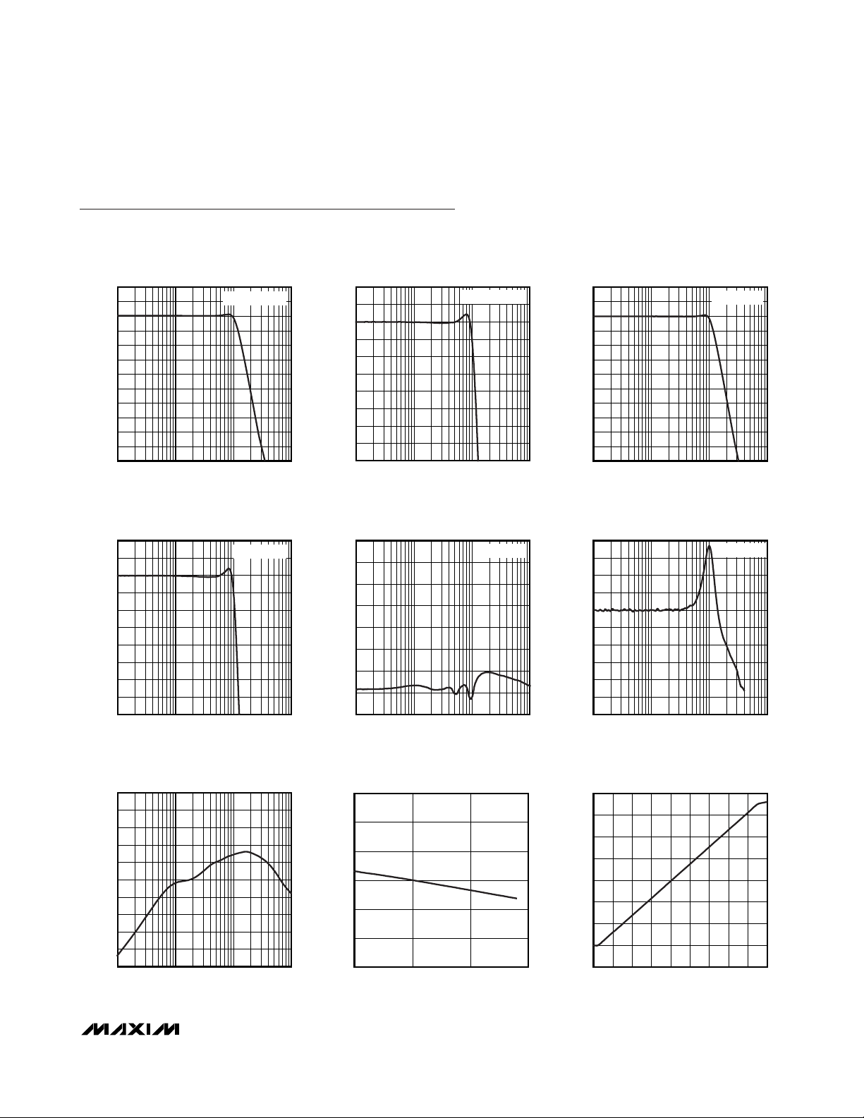
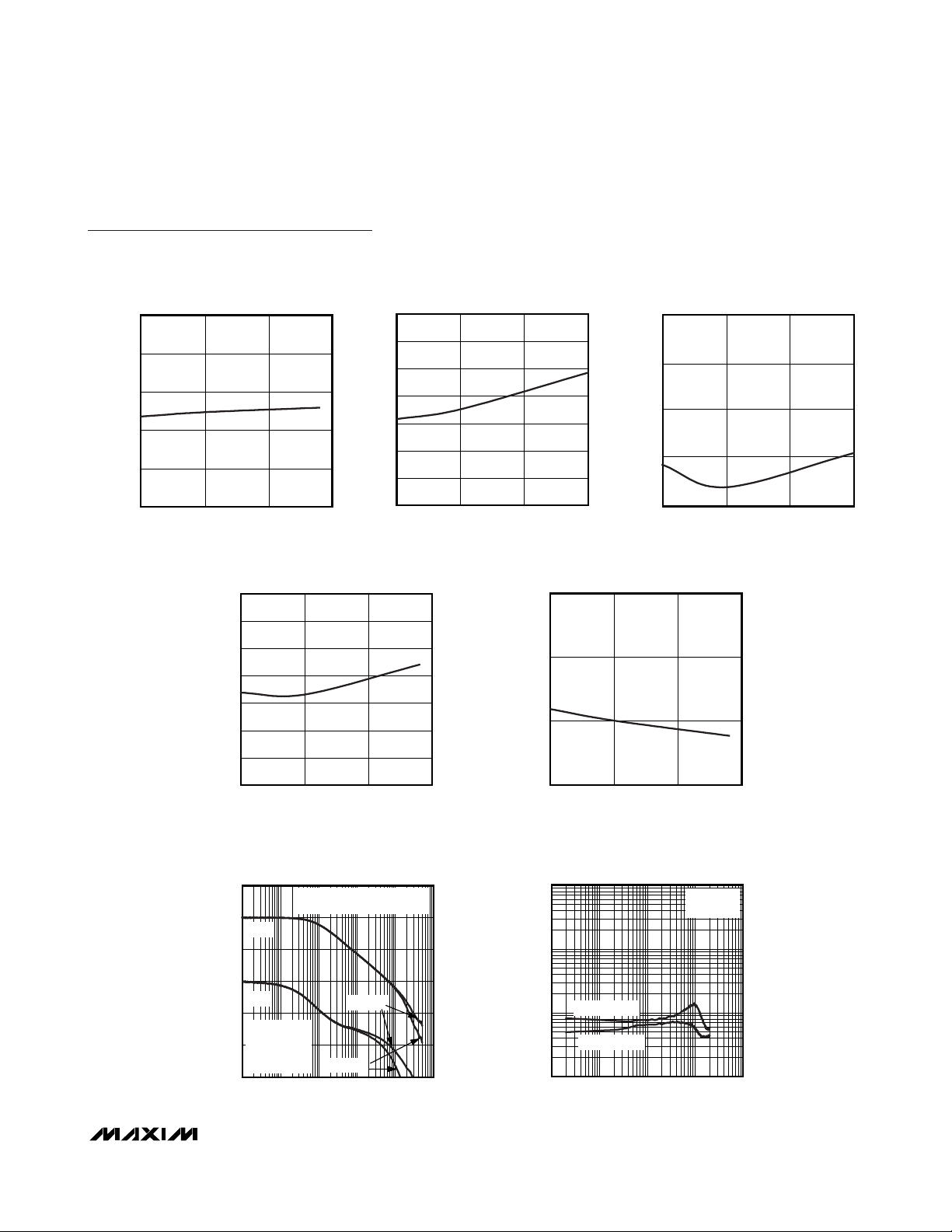
Typical Operating Characteristics
(V
VID
= V
AUD
= 3.3V, V12= 12V, GND = EP = 0, video load is 150Ω to GND, audio load is 10kΩ to GND, TA= +25°C, unless other-
wise noted.)
VIDEO SMALL-SIGNAL GAIN
vs. FREQUENCY
10
5
0
-5
-10
-15
-20
GAIN (dB)
-25
-30
-35
-40
-45
-50
100k 100M
FREQUENCY (Hz)
VIDEO LARGE-SIGNAL GAIN FLATNESS
vs. FREQUENCY
2
1
0
-1
-2
-3
GAIN (dB)
-4
-5
-6
-7
-8
FREQUENCY (Hz)
V
= 100mV
OUT
10M1M
10M1M100k 100M
P-P
V
= 2V
OUT
P-P
MAX9597 toc01
MAX9597 toc04
VIDEO SMALL-SIGNAL GAIN FLATNESS
2
1
0
-1
-2
-3
GAIN (dB)
-4
-5
-6
-7
-8
VIDEO CROSSTALK vs. FREQUENCY
0
-10
-20
-30
-40
-50
CROSSTALK (dB)
-60
-70
-80
vs. FREQUENCY
FREQUENCY (Hz)
FREQUENCY (Hz)
V
= 100mV
OUT
10M1M100k 100M
10M1M100k 100M
P-P
V
= 2V
OUT
P-P
MAX9597 toc02
GAIN (dB)
MAX9597 toc05
GROUP DELAY (ns)
VIDEO LARGE-SIGNAL GAIN
vs. FREQUENCY
10
5
0
-5
-10
-15
-20
-25
-30
-35
-40
-45
-50
FREQUENCY (Hz)
VIDEO GROUP DELAY DISTORTION
vs. FREQUENCY
100
90
80
70
60
50
40
30
20
10
0
FREQUENCY (Hz)
V
= 2V
OUT
P-P
10M1M100k 100M
V
= 2V
OUT
P-P
10M1M100k 100M
MAX9597 toc03
MAX9597 toc06
VIDEO POWER-SUPPLY REJECTION RATIO
vs. FREQUENCY
0
-5
-10
-15
-20
-25
PSRR (dB)
-30
-35
-40
-45
-50
FREQUENCY (Hz)
10M1M100k 100M
MAX9597 toc07
VOLTAGE GAIN (V/V)
VOLTAGE GAIN
vs. TEMPERATURE
2.03
2.02
2.01
2.00
1.99
1.98
1.97
0 255075
TEMPERATURE (°C)
MAX9597 toc08
OUTPUT VOLTAGE (V)
-0.5
VIDEO OUTPUT VOLTAGE
vs. INPUT VOLTAGE
3.5
3.0
2.5
2.0
1.5
1.0
0.5
0
-0.2 1.6
INPUT VOLTAGE (V)
MAX9597 toc09
1.41.20 0.2 0.4 0.80.6 1.0
Page 8
MAX9597
Low-Power Audio/Video Interface
for Single SCART Connectors
8 _______________________________________________________________________________________
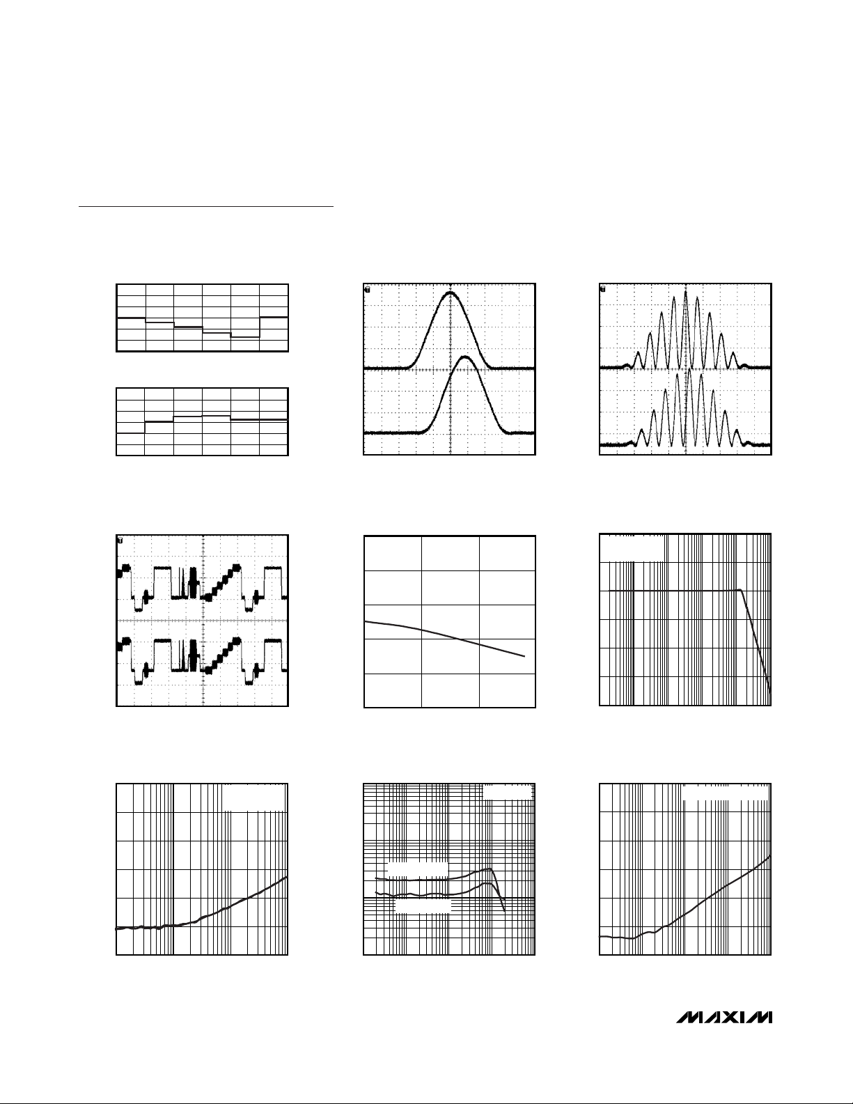
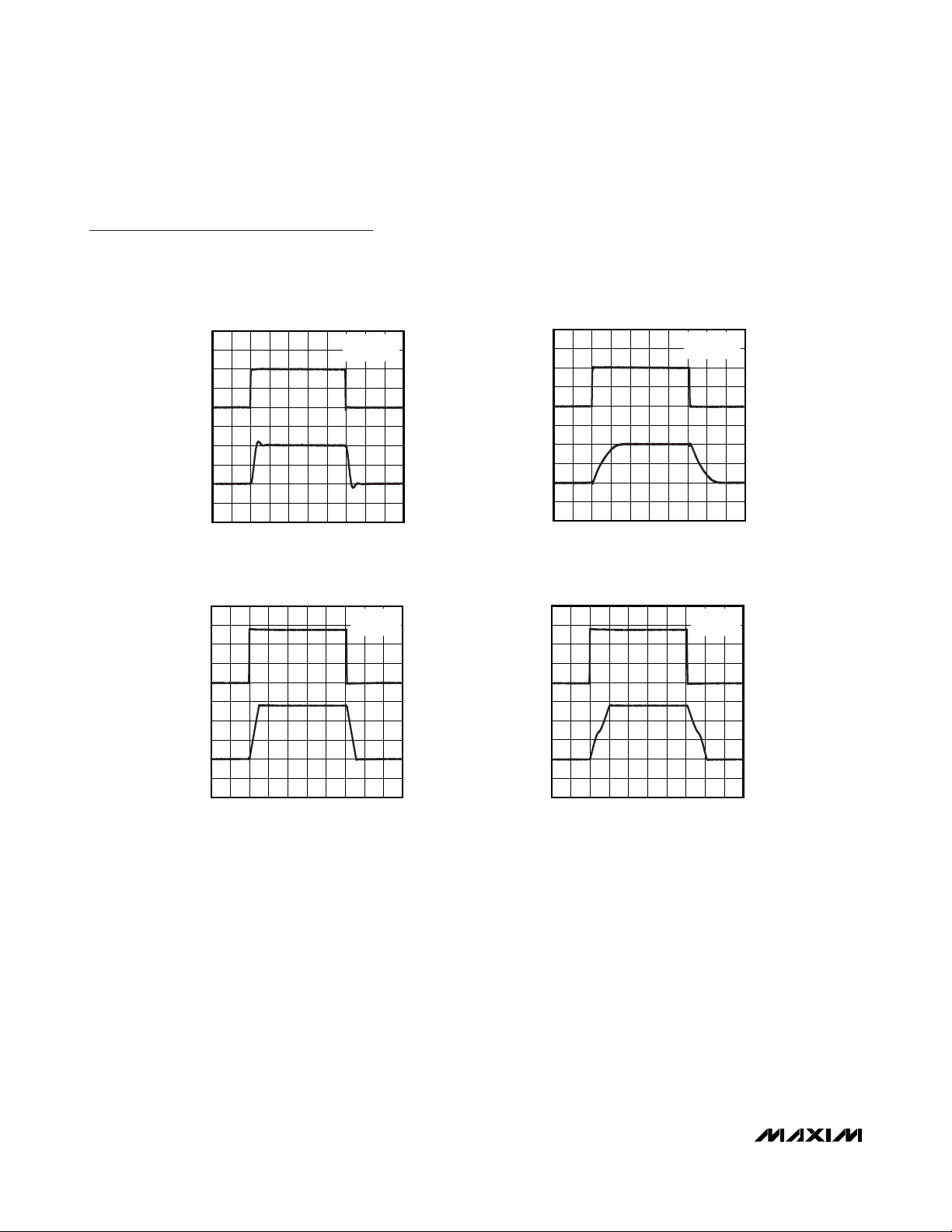
Typical Operating Characteristics (continued)
(V
VID
= V
AUD
= 3.3V, V12= 12V, GND = EP = 0, video load is 150Ω to GND, audio load is 10kΩ to GND, TA= +25°C, unless other-
wise noted.)
DIFFERENTIAL GAIN AND PHASE
MAX9597 toc10
DIFFERENTIAL PHASE (deg)
103245
0.6
0.8
0.4
0.2
0
-0.2
-0.4
DIFFERENTIAL GAIN (%)
0.2
0.3
0.1
0
-0.1
-0.2
-0.3
103245
100ns/div
2T RESPONSE
INPUT
200mV/div
MAX9597 toc11
OUTPUT
400mV/div
400ns/div
12.5T RESPONSE
INPUT
200mV/div
MAX9597 toc12
OUTPUT
400mV/div
10
μs/div
PAL VIDEO TEST SIGNAL
INPUT
0.5V/div
MAX9597 toc13
OUTPUT
1V/div
1.460
1.464
1.472
1.468
1.476
1.480
VIDEO OUTPUT BIAS VOLTAGE
vs. TEMPERATURE
MAX9597 toc14
TEMPERATURE (°C)
VIDEO OUTPUT BIAS VOLTAGE (V)
0255075
AUDIO LARGE-SIGNAL BANDWIDTH
vs. FREQUENCY
MAX9597 toc15
FREQUENCY (Hz)
GAIN (dB)
100k10k1k100
-15
-10
-5
0
5
10
-20
10 1M
VIN = 0.25V
RMS
RL = 10kΩ
AUDIO CROSSTALK
vs. FREQUENCY
MAX9597 toc16
FREQUENCY (Hz)
CROSSTALK (dB)
10k1k
-100
-80
-60
-40
-20
0
-120
100 100k
VIN = 0.25V
RMS
RL = 10kΩ
TOTAL HARMONIC DISTORTION
PLUS NOISE vs. FREQUENCY
MAX9597 toc17
FREQUENCY (Hz)
THD+N (%)
10k1k100
0.001
0.01
0.1
0.0001
10 100k
RL = 3.3kΩ
VIN = 0.25V
RMS
VIN = 0.5V
RMS
V
AUD
POWER-SUPPLY REJECTION RATIO
(INPUT REFERRED) vs. FREQUENCY
MAX9597 toc18
FREQUENCY (Hz)
PSRR (dB)
10k1k100
-100
-80
-60
-40
-20
0
-120
10 100k
V
AUD
= 3.3V + 100mV
P-P
Page 9
MAX9597
Low-Power Audio/Video Interface
for Single SCART Connectors
_______________________________________________________________________________________
9
Typical Operating Characteristics (continued)
(V
VID
= V
AUD
= 3.3V, V12= 12V, GND = EP = 0, video load is 150Ω to GND, audio load is 10kΩ to GND, TA= +25°C, unless other-
wise noted.)
INPUT-AMPLIFIER TOTAL HARMONIC
DISTORTION PLUS NOISE vs. FREQUENCY
MAX9597 toc25
FREQUENCY (Hz)
THD+N (%)
100 10k1k
0.001
0.01
0.1
0.0001
10 100k
VIN = 0.25V
RMS
VIN = 0.5V
RMS
UNITY GAIN
R
L
= OPEN
2.9
3.1
3.0
3.3
3.2
3.5
3.4
3.6
0255075
V
AUD
QUIESCENT SUPPLY CURRENT
vs. TEMPERATURE
MAX9597 toc20
TEMPERATURE (°C)
QUIESCENT SUPPLY CURRENT (mA)
V
QUIESCENT SUPPLY CURRENT
VID
14.3
14.2
14.1
14.0
13.9
QUIESCENT SUPPLY CURRENT (mA)
13.8
0255075
vs. TEMPERATURE
TEMPERATURE (°C)
INPUT-AMPLIFIER INPUT OFFSET
VOLTAGE vs. TEMPERATURE
20
15
10
5
V12 QUIESCENT SUPPLY CURRENT
vs. TEMPERATURE
0.20
MAX9597 toc19
INPUT-AMPLIFIER INPUT BIAS CURRENT
0.3
MAX9597 toc22
0.2
0.15
0.10
0.05
QUIESCENT SUPPLY CURRENT (μA)
0
0255075
TEMPERATURE (°C)
vs. TEMPERATURE
MAX9597 toc23
MAX9597 toc21
0
-5
INPUT OFFSET VOLTAGE (mV)
-10
-15
0255075
TEMPERATURE (°C)
0.1
INPUT BIAS CURRENT (μA)
0
-50 25 50 75
TEMPERATURE (°C)
INPUT-AMPLIFIER GAIN AND PHASE
60
40
GAIN
20
0
GAIN (dB)
PHASE
-20
AV = +100V/V
V
-40
R
C
-60
1k 100M
PHASE MARGIN (CL = 0pF) = 60°
PHASE MARGIN (C
= 10mV
IN
P-P
= OPEN
LOAD
= 0pF/22pF
L
FREQUENCY (Hz)
CL = OpF
CL = 22pF
vs. FREQUENCY
= 22pF) = 44°
L
10M1M100k10k
180
120
MAX9597 toc24
60
0
PHASE (deg)
-60
-120
-180
Page 10
MAX9597
Low-Power Audio/Video Interface
for Single SCART Connectors
10 ______________________________________________________________________________________
Typical Operating Characteristics (continued)
(V
VID
= V
AUD
= 3.3V, V12= 12V, GND = EP = 0, video load is 150Ω to GND, audio load is 10kΩ to GND, TA= +25°C, unless other-
wise noted.)
0V
OUTPUT
50mV/div
0V
INPUT-AMPLIFIER SMALL-SIGNAL
TRANSIENT RESPONSE
MAX9597 toc26
200ns/div
UNITY GAIN
R
L
= OPEN
INPUT
50mV/div
0V
OUTPUT
50mV/div
0V
INPUT-AMPLIFIER SMALL-SIGNAL
TRANSIENT RESPONSE
MAX9597 toc27
200ns/div
UNITY GAIN
R
L
= 124Ω
INPUT
50mV/div
0V
OUTPUT
500mV/div
0V
INPUT-AMPLIFIER LARGE-SIGNAL
TRANSIENT RESPONSE
MAX9597 toc28
1μs/div
UNITY GAIN
R
L
= OPEN
INPUT
500mV/div
0V
OUTPUT
500mV/div
0V
INPUT-AMPLIFIER LARGE-SIGNAL
TRANSIENT RESPONSE
MAX9597 toc29
1μs/div
UNITY GAIN
R
L
= 124Ω
INPUT
500mV/div
Page 11

MAX9597
Low-Power Audio/Video Interface
for Single SCART Connectors
______________________________________________________________________________________ 11
Pin Description
PIN NAME FUNCTION
1V
2 C1P Charge-Pump Flying Capacitor Positive Terminal. Connect a 1μF capacitor from C1P to C1N.
3 C1N Charge-Pump Flying Capacitor Negative Terminal. Connect a 1μF capacitor from C1P to C1N.
4 CPVSS
5 DEV_ADDR Device Address Set Input. Connect DEV_ADDR to GND, V
6 SDA Bidirectional, I2C Data I/O. Output is open drain and tolerates up to 3.6V.
7 SCL I2C Clock Input
8 ENC_B_IN Encoder Blue Video Input
9 ENC_G_IN Encoder Green Video Input
10 ENC_R/C_IN Encoder Red/Chroma Video Input
11 ENC_CVBS_IN Encoder Composite Video Input
12 TV_CVBS_OUT TV SCART Composite Video Output. The sync tip is biased at 0.3V.
13 V
14 TV_FS_OUT
15 GND Video Ground
16 TV_R/C_OUT
17 TV_G_OUT TV SCART Green Video Output. The black level of the green signal is set to 0.3V.
18 TV_B_OUT TV SCART Blue Video Output. The black level of the blue signal is set to 0.3V.
19 V
20 TV_SS_OUT TV SCART Slow-Switch Signal Output
21 TV_OUTL TV SCART Left-Channel Audio Output
22 ENC_INL+ Left Input-Amplifier Noninverting Terminal
23 ENC_INL- Left Input-Amplifier Inverting Terminal
24 ENC_INLOUT Left Input-Amplifier Output
25 ENC_INROUT Right Input-Amplifier Output
26 ENC_INR- Right Input-Amplifier Noninverting Terminal
27 ENC_INR+ Right Input-Amplifier Inverting Terminal
28 TV_OUTR TV SCART Right-Channel Audio Output
—EP
AUD
VID
12
Audio Supply. Connect to a 3.3V supply. Bypass with a 10μF aluminum electrolytic capacitor in
parallel with a 0.1μF ceramic capacitor to EP.
Charge-Pump Negative Power Supply. Bypass with a 10μF aluminum electrolytic capacitor in
parallel with a 1μF ceramic capacitor to EP.
, SDA, or SCL. See Table 3.
VID
Video and Digital Supply. Connect to a +3.3V supply. Bypass with a parallel 1μF and 0.1μF
ceramic capacitor to GND. V
TV SCART Fast-Switching Logic Output. This signal drives a back-terminated, 75Ω transmission
line.
TV SCART Red/Chroma Video Output. The black level of the red signal is set to 0.3V and the
blank level of the chroma signal is 1.5V.
+12V Supply. Bypass V12 with a 0.1μF capacitor to EP.
Exposed Pad. The exposed pad is the internal ground for the audio amplifiers and charge pump.
A low-impedance connection to EP is required for proper isolation.
also serves as a digital supply for the I2C interface.
VID
Page 12

MAX9597
Low-Power Audio/Video Interface
for Single SCART Connectors
12 ______________________________________________________________________________________
Detailed Description
The MAX9597 represents Maxim’s third generation of
SCART audio/video (A/V) switches. Under I2C control,
these devices route audio, video, and control information between the set-top box decoder chip and a
SCART connector. The audio signals are left audio and
right audio. The video signals are composite video with
blanking and sync (CVBS) and component video (red,
green, blue). S-video (Y/C) can be transported across
the SCART interface if CVBS is reassigned to luma (Y)
and red is reassigned to chroma (C). Support for
S-video is optional. The slow-switch signal and the fastswitch signal carry control information. The slow-switch
signal is a 12V, trilevel signal that indicates whether the
picture aspect ratio is 4:3, 16:9, or causes the television
to use an internal A/V source, such as an antenna. The
fast-switch signal indicates whether the television
should display CVBS or RGB signals.
CVBS, left audio, and right audio are full duplex. All the
other signals are half duplex. Therefore, one device on
the link must be designated as the transmitter, and the
other device must be designated as the receiver.
The low power consumption of the MAX9597 enables
the creation of lower power set-top boxes, televisions,
and DVD players. Unlike competing SCART ICs, the
audio and video circuits of the MAX9597 operate entirely
from 3.3V rather than from 5V and 12V. Only the slowswitch circuit of the MAX9597 requires a 12V supply.
The MAX9597 features DirectDrive audio circuitry to
eliminate click-and-pop noise. With DirectDrive, the DC
bias of the audio line outputs is always at ground when
the MAX9597 is being powered up or powered down.
Conventional audio line output drivers that operate from
a single supply require series AC-coupling capacitors.
During power-up, the DC bias on the AC-coupling
capacitor moves from ground to a positive voltage, and
during power-down, the opposite occurs. The changing
DC bias usually causes an audible transient.
Audio Section
The audio circuit consists of a left and right audio path,
each with an independent operational amplifier followed by a gain-of-4 amplifier. The encoder (stereo
audio DAC) is the input source, and the output goes to
the TV SCART connector. See Figure 1.
Figure 1. MAX9597 Audio Section Functional Diagram
ENC_INR+
INPUT
ENC_INR-
ENC_INROUT
OP AMP
ZERO-CROSS
DETECTOR
V
AUD
EP
= 4V/V
A
V
TV_OUTR
ENC_INL+
INPUT
ENC_INL-
ENC_INLOUT
V
AUD
C1P
C1N
CPVSS
EP
OP AMP
CHARGE
PUMP
ZERO-CROSS
DETECTOR
V
AUD
EP
A
= 4V/V
V
MAX9597
TV_OUTL
Page 13

MAX9597
Low-Power Audio/Video Interface
for Single SCART Connectors
______________________________________________________________________________________ 13
The full-scale output of the independent operational
amplifiers is 0.5V
RMS
. The closed-loop gain of the operational amplifier circuit should be designed such that
the resulting full-scale output is 0.5V
RMS
. The fixed,
gain-of-4 amplifiers that follow the independent operational amplifiers amplify the 0.5V
RMS
to 2V
RMS
, which
complies with the SCART standard.
An integrated charge pump inverts the +3.3V supply
(V
AUD
) to create a -3.3V supply (CPVSS), enabling the
audio circuit to operate from bipolar supplies. The
audio signal from the beginning to the end of the signal
path is always biased at ground.
Clickless Muting and Unmuting
The TV audio channel incorporates a zero-crossing
detect (ZCD) circuit that minimizes click noise due to
abrupt signal level changes that occur when entering
or coming out of a mute condition at an arbitrary
moment.
To implement the zero-crossing function when switching audio signals, set ZCD (register 00h, bit 6) high.
The MAX9597 switches the signal in or out of mute at
the next zero crossing after the mute or unmute request
occurs. See Table 8.
Audio Outputs
The MAX9597 audio output amplifiers feature Maxim’s
patented† DirectDrive architecture, eliminating the need
for output-coupling capacitors required by conventional
single-supply audio line drivers. Conventional singlesupply audio line drivers have their outputs biased
about a nominal DC voltage (typically half the supply)
for maximum dynamic range. Large coupling capacitors are needed to block this DC bias. Clicks and pops
are created when the coupling capacitors are charged
during power-up and discharged during power-down.
An internal charge pump inverts the positive supply
(V
AUD
), creating a negative supply (CPVSS). The audio
output amplifiers operate from the bipolar supplies with
the outputs biased about audio ground (Figure 2). The
benefit of this audio ground bias is that the amplifier
outputs do not have a DC component. The DC-blocking
capacitors required with conventional audio line drivers
are unnecessary, conserving board space, reducing
system cost, and improving frequency response.
The MAX9597 features a low-noise charge pump that
requires only two small ceramic capacitors. The
580kHz switching frequency is well beyond the audio
range and does not interfere with audio signals. The
switch drivers feature a controlled switching speed that
minimizes noise generated by turn-on and turn-off transients. The di/dt noise caused by the parasitic bond
wire and trace inductance is minimized by limiting the
switching speed of the charge pump.
The SCART standard specifies 2V
RMS
as the full-scale
for audio signals. As the audio circuits process
0.5V
RMS
full-scale audio signals internal to the
MAX9597, the gain-of-4 output amplifiers restore the
audio signals to a full scale of 2V
RMS
.
Video Section
The video circuit routes different video formats between
the set-top box decoder and the TV SCART connector.
It also routes slow-switch and fast-switch control information as shown in Figure 3.
Video Inputs
Whether the incoming video input signal is AC-coupled
or DC-coupled into the MAX9597 depends upon the origin, format, and voltage range of the video signal. Table
1 below shows the recommended connections. Always
AC-couple an external video signal through a 0.1μF
capacitor because its voltage range is not well defined
(see the
Typical Application Circuit
). For example, the
Figure 2. Conventional Driver Output Waveform vs. MAX9597
Output Waveform
†
U.S. Patent #7,061,327
V
DD
V
OUT
CONVENTIONAL DRIVER-BIASING SCHEME
V
OUT
DirectDrive BIASING SCHEME
VDD/2
GND
+V
DD
GND
-V
DD
Page 14

MAX9597
Low-Power Audio/Video Interface
for Single SCART Connectors
14 ______________________________________________________________________________________
video transmitter circuit might have a different ground
than the video receiver, thereby level shifting the DC
bias. The 50Hz power line hum might cause the video
signal to change DC bias slowly.
Internal video signals that are between 0V and 1V can
be DC-coupled. Most video DACs generate video signals between 0V and 1V because the video DAC
sources current into a ground-referenced resistor. For
the minority of video DACs that generate video signals
between 2.3V and 3.3V because the video DAC sinks
current from a VDD-referenced resistor, AC-couple the
video signal to the MAX9597.
The MAX9597 restores the DC level of incoming,
AC-coupled video signals with either transparent synctip clamps or bias circuits. When using an AC-coupled
input, the transparent sync-tip clamp automatically
clamps the input signal minimum to ground, preventing it
from going lower. A small current of 2μA pulls down on
the input to prevent an AC-coupled signal from drifting
outside the input range of the part. The transparent synctip clamp is used with CVBS, RGB, and luma signals.
The transparent sync-tip clamp is transparent when the
incoming video signal is DC-coupled and at ground or
above. Under such conditions, the clamp never activates. Therefore, the outputs of video DACs that generate signals between 0V and 1V can be directly
connected to the MAX9597 inputs.
The bias circuit accepts AC-coupled chroma, which is
a subcarrier with the color information modulated onto
it. The bias voltage of the bias circuits is around
600mV.
ENC_R/C_IN can receive either a red video signal or a
chroma video signal. Set the input configuration by writing to bit 3 of register 08h. See Table 10.
Figure 3. MAX9597 Video Section Function Diagram
ENC_CVBS_IN
ENC_R/C_IN
ENC_G_IN
ENC_B_IN
CLAMP
CLAMP/BIAS
CLAMP
CLAMP
V
GND
VID
V
+6V
LPF
LPF
LPF
LPF
12
EP
MAX9597
A
A
A
A
A
A
= 2V/V
V
= 2V/V
V
= 2V/V
V
= 2V/V
V
= 1V/V
V
= 1V/V
V
TV_CVBS_OUT
TV_R/C_OUT
TV_G_OUT
TV_B_OUT
TV_FS_OUT
TV_SS_OUT
Page 15

MAX9597
Low-Power Audio/Video Interface
for Single SCART Connectors
______________________________________________________________________________________ 15
Video Reconstruction Filter
The video DAC outputs of the set-top box decoder chip
need to be lowpass-filtered to reject the out-of-band
noise. The MAX9597 integrates sixth-order, Butterworth
filters. The filter passband (±1dB) is typically 10MHz,
and the attenuation at 27MHz is 43dB. The filters are
suited for standard-definition video.
Video Outputs
The video output amplifiers can both source and sink
load current, allowing output loads to be DC- or
AC-coupled. The amplifier output stage needs approximately 300mV of headroom from either supply rail.
If the supply voltage is greater than 3.135V (5% below
a 3.3V supply), each amplifier can drive two DC-coupled video loads to ground. If the supply is less than
3.135V, each amplifier can drive only one DC-coupled
or AC-coupled video load.
The SCART standard allows for video signals to have a
superimposed DC component within 0V and 2V.
Therefore, most video signals are DC-coupled at the output. In the unlikely event that the video signal needs to
be AC-coupled, the coupling capacitors should be
220μF or greater to keep the highpass filter formed by
the 37.5Ω equivalent resistance of the video transmission line to a corner frequency of 4.8Hz or below to keep
it well below the 25Hz frame rate of the PAL standard.
The video outputs can be enabled or disabled by bits 1
to 5 of register 0Dh. See Table 11.
Slow Switching
The MAX9597 supports the IEC 933-1, Amendment 1,
trilevel slow-switching standard that selects the aspect
ratio for the display (TV). Under I2C control, the
MAX9597 sets the slow-switching output voltage level.
Table 2 shows the valid input levels of the slow-switching signal and the corresponding operating modes of
the display device.
One port is available for slow-switching signals for the
TV. The slow-switching outputs can be set to a logic
level or high impedance by writing to bit 0 and 1 of register 07h. See Table 9.
Table 1. Recommended Coupling for Incoming Video Signals and Input Circuit
Configuration**
**
Use a 0.1μF capacitor to AC-couple a video signal into the MAX9597.
Table 2. Slow-Switching Modes
VIDEO ORIGIN FORMAT
External CVBS Unknown AC Transparent sync-tip clamp
External RGB Unknown AC Transparent sync-tip clamp
External Y Unknown AC Transparent sync-tip clamp
External C Unknown AC Bias circuit
Internal CVBS 0 to 1 DC Transparent sync-tip clamp
Internal R, G, B 0 to 1 DC Transparent sync-tip clamp
Internal Y, C 0 to 1 DC Transparent sync-tip clamp
Internal Y, Pb, Pr 0 to 1 DC Transparent sync-tip clamp
Internal CVBS 2.3 to 3.3 AC Transparent sync-tip clamp
Internal R, G, B 2.3 to 3.3 AC Transparent sync-tip clamp
Internal Y 2.3 to 3.3 AC Transparent sync-tip clamp
Internal C 2.3 to 3.3 AC Bias circuit
VOLTAGE RANGE
(V)
COUPLING INPUT CIRCUIT CONFIGURATION
SLOW-SWITCHING
SIGNAL VOLTAGE
(V)
0 to 2
4.5 to 7.0
9.5 to 12.6
Display device uses an internal
source such as a built-in tuner to
provide a video signal.
Display device uses a video signal
from the SCART connector and sets
the display to a 16:9 aspect ratio.
Display device uses a signal from the
SCART connector and sets the
display to a 4:3 aspect ratio.
MODE
Page 16

MAX9597
Low-Power Audio/Video Interface
for Single SCART Connectors
16 ______________________________________________________________________________________
Fast Switching
The fast-switching signal was originally used to switch
between CVBS and RGB signals on a pixel-by-pixel
basis so that on-screen display (OSD) information
could be inserted. Since modern set-top box decoder
chips have integrated OSD circuitry, there is no need to
create OSD information using the older technique.
Now, the fast-switching signal is just used to switch
between CVBS and RGB signal sources.
Set the source of the fast-switching signal by writing to
bits 4 and 3 of register 07h. The fast-switching signal to
the TV SCART connector can be enabled or disabled
by bit 1 of register 0Dh. See Tables 9 and 11.
I2C Serial Interface
The MAX9597 features an I2C/SMBus™-compatible,
2-wire serial interface consisting of a serial-data line
(SDA) and a serial-clock line (SCL). SDA and SCL facilitate communication between the MAX9597 and the master at clock rates up to 400kHz. Figure 4 shows the
2-wire interface timing diagram. The master generates
SCL and initiates data transfer on the bus. A master
device writes data to the MAX9597 by transmitting a
START (S) condition, the proper slave address with the
R/W bit set to 0, followed by the register address and
then the data word. Each transmit sequence is framed
by a START and a STOP (P) condition. Each word transmitted to the MAX9597 is 8 bits long and is followed by
an acknowledge clock pulse. A master reads from the
MAX9597 by transmitting the slave address with the R/W
bit set to 0, the register address of the register to be
read, a REPEATED START (Sr) condition, the slave
address with the R/W bit set to 1, followed by a series of
SCL pulses. The MAX9597 transmits data on SDA in
sync with the master-generated SCL pulses. The master
acknowledges receipt of each byte of data. Each read
sequence is framed by a START or REPEATED START
condition, an acknowledge or a not acknowledge, and a
STOP condition. SDA operates as both an input and an
open-drain output. A pullup resistor, typically greater
than 500Ω, is required on the SDA bus. SCL operates as
only an input. A pullup resistor, typically greater than
500Ω, is required on SCL if there are multiple masters on
the bus, or if the master in a single-master system has an
open-drain SCL output. Series resistors in line with SDA
and SCL are optional. Series resistors protect the digital
inputs of the MAX9597 from high-voltage spikes on the
bus lines, and minimize crosstalk and undershoot of the
bus signals.
Bit Transfer
One data bit is transferred during each SCL cycle. The
data on SDA must remain stable during the high period
of the SCL pulse. Changes in SDA while SCL is high
are control signals (see the
START and STOP
Table 3. Slave Address
Figure 4. I2C Serial-Interface Timing Diagram
SMBus is a trademark of Intel Corp.
DEV_ADDR B7 B6 B5 B4 B3 B2 B1 B0
GND 1001010R/W 94h 95h
V
VID
SCL 1001100R/W 98h 99h
SDA 1001101R/W 9Ah 9Bh
1001011R/W 96h 97h
SDA
t
SU, STA
REPEATED
START CONDITION
t
HD, STA
SCL
t
HD, STA
START
CONDITION
t
LOW
t
SU, DAT
t
HD, DAT
t
HIGH
t
R
t
F
WRITE ADDRESS
(HEX)
t
SP
t
SU, STO
READ ADDRESS
t
BUF
STOP
CONDITION
(HEX)
START
CONDITION
Page 17

MAX9597
Low-Power Audio/Video Interface
for Single SCART Connectors
______________________________________________________________________________________ 17
Conditions
section). SDA and SCL idle high when the
I2C bus is not busy.
START and STOP Conditions
SDA and SCL idle high when the bus is not in use. A
master initiates communication by issuing a START condition. A START condition is a high-to-low transition on
SDA with SCL high. A STOP condition is a low-to-high
transition on SDA while SCL is high (Figure 5). A START
condition from the master signals the beginning of a
transmission to the MAX9597. The master terminates
transmission, and frees the bus, by issuing a STOP condition. The bus remains active if a REPEATED START
condition is generated instead of a STOP condition.
Early STOP Conditions
The MAX9597 recognizes a STOP condition at any
point during data transmission except if the STOP condition occurs in the same high pulse as a START condition. For proper operation, do not send a STOP
condition during the same SCL high pulse as the
START condition.
Slave Address
The slave address is defined as the 7 most significant
bits (MSBs) followed by the read/write (R/W) bit. Set the
R/W bit to 1 to configure the MAX9597 to read mode.
Set the R/W bit to 0 to configure the MAX9597 to write
mode. The slave address is always the first byte of
information sent to the MAX9597 after a START or a
REPEATED START condition. The MAX9597 slave
address is configurable with DEV_ADDR. Table 3
shows the possible slave addresses for the MAX9597.
Acknowledge
The acknowledge bit (ACK) is a clocked 9th bit that the
MAX9597 uses to handshake receipt of each byte of
data when in write mode (see Figure 6). The MAX9597
pulls down SDA during the entire master-generated
ninth clock pulse if the previous byte is successfully
received. Monitoring ACK allows for detection of unsuccessful data transfers. An unsuccessful data transfer
occurs if a receiving device is busy or if a system fault
has occurred. In the event of an unsuccessful data
transfer, the bus master may retry communication. The
master pulls down SDA during the ninth clock cycle to
acknowledge receipt of data when the MAX9597 is in
read mode. An acknowledge is sent by the master after
each read byte to allow data transfer to continue. A not
acknowledge is sent when the master reads the final
byte of data from the MAX9597, followed by a STOP
condition.
Write Data Format
A write to the MAX9597 consists of transmitting a
START condition, the slave address with the R/W bit set
to 0, one data byte to configure the internal register
address pointer, one or more data bytes, and a STOP
condition. Figure 7 illustrates the proper frame format
for writing one byte of data to the MAX9597. Figure 8
illustrates the frame format for writing n-bytes of data to
the MAX9597.
The slave address with the R/W bit set to 0 indicates
that the master intends to write data to the MAX9597.
The MAX9597 acknowledges receipt of the address
byte during the master-generated ninth SCL pulse.
The second byte transmitted from the master configures the MAX9597’s internal register address pointer.
The pointer tells the MAX9597 where to write the next
byte of data. An acknowledge pulse is sent by the
MAX9597 upon receipt of the address pointer data.
The third byte sent to the MAX9597 contains the data
that is written to the chosen register. An acknowledge
pulse from the MAX9597 signals receipt of the data
byte. The address pointer autoincrements to the next
Figure 5. START, STOP, and REPEATED START Conditions
Figure 6. Acknowledge
SSrP
SCL
SDA
CLOCK PULSE FOR
START
CONDITION
SCL
SDA
1
289
ACKNOWLEDGMENT
NOT ACKNOWLEDGE
ACKNOWLEDGE
Page 18

MAX9597
Low-Power Audio/Video Interface
for Single SCART Connectors
18 ______________________________________________________________________________________
register address after each received data byte. This
autoincrement feature allows a master to write to
sequential register address locations within one continuous frame. The master signals the end of transmission
by issuing a STOP condition.
Read Data Format
The master presets the address pointer by first sending
the MAX9597’s slave address with the R/W bit set to 0
followed by the register address after a START condition. The MAX9597 acknowledges receipt of its slave
address and the register address by pulling SDA low
during the ninth SCL clock pulse. A REPEATED START
condition is then sent followed by the slave address
with the R/W bit set to 1. The MAX9597 transmits the
contents of the specified register. Transmitted data is
valid on the rising edge of the master-generated serial
clock (SCL). The address pointer autoincrements after
each read data byte. This autoincrement feature allows
all registers to be read sequentially within one continuous frame. A STOP condition can be issued after any
number of read data bytes. If a STOP condition is
issued followed by another read operation, the first
data byte to be read is from the register address location set by the previous transaction and not 00h and
subsequent reads autoincrement the address pointer
until the next STOP condition. Attempting to read from
register addresses higher than 01h results in repeated
reads from a dummy register containing FFh data. The
master acknowledges receipt of each read byte during
the acknowledge clock pulse. The master must
acknowledge all correctly received bytes except the
last byte. The final byte must be followed by a not
acknowledge from the master and then a STOP condition. Figures 9 and 10 illustrate the frame format for
reading data from the MAX9597.
Applications Information
Operating Modes
The MAX9597 has two operating modes: full power
and shutdown. The operations can be set by writing to
bit 7 of register 10h. See Table 12.
In shudown mode, all circuitry is shut down except for
the I
2
C interface, which is designed with static CMOS
logic. If the I2C bus is quiet, the I2C interface draws
only leakage current.
Power Consumption
With a low 3.3V supply, the quiescent power consumption and average power consumption of the MAX9597
is very low. Quiescent power consumption is defined
Figure 7. Writing a Byte of Data to the MAX9597
Figure 8. Writing n-Bytes of Data to the MAX9597
ACKNOWLEDGE FROM MAX9597
S AA
0SLAVE ADDRESS REGISTER ADDRESS DATA BYTE
ACKNOWLEDGE FROM MAX9597
ACKNOWLEDGE FROM MAX9597
B1 B0B3 B2B5 B4B7 B6
A
P
R/W
ACKNOWLEDGE FROM MAX9597
S
SLAVE ADDRESS
R/W
ACKNOWLEDGE FROM MAX9597
A
REGISTER ADDRESS
ACKNOWLEDGE FROM MAX9597
A
DATA BYTE 1
1 BYTE
AUTOINCREMENT INTERNAL
REGISTER ADDRESS POINTER
1 BYTE
AUTOINCREMENT INTERNAL
REGISTER ADDRESS POINTER
ACKNOWLEDGE FROM MAX9597
B1 B0B3 B2B5 B4B7 B6
A0
DATA BYTE n
1 BYTE
B1 B0B3 B2B5 B4B7 B6
A
P
Page 19
MAX9597
Low-Power Audio/Video Interface
for Single SCART Connectors
______________________________________________________________________________________ 19
when the MAX9597 is operating without loads and without any audio or video signals. Table 4 shows the quiescent power consumption in both operating modes.
Average power consumption is defined when the
MAX9597 drives typical signals into typical loads. Table 5
shows the average power consumption in full-power
mode, and Table 6 shows the input and output conditions.
Interfacing to an RF Modulator
If the set-top box modulates CVBS and mono audio
onto an RF carrier (for example, channel 3), a simple
application circuit can provide the needed signals (see
Figure 11). A 10kΩ resistor summer circuit between
TV_OUTR and TV_OUTL creates the mono audio signal. The resistor-divider to ground on TV_CVBS_OUT
creates a video signal with normal amplitude. The
unique feature of the MAX9597 that facilitates this
application circuit is that the audio and video output
amplifiers of the MAX9597 can drive multiple loads if
V
AUD
and V
VID
are both greater than 3.135V.
Floating-Chassis Discharge Protection
and ESD
Some set-top boxes have a floating chassis problem in
which the chassis is not connected to earth ground. As
a result, the chassis can charge up to 500V. When a
SCART cable is connected to the SCART connector,
the charged chassis can discharge through a signal
pin. The equivalent circuit is a 2200pF capacitor
charged to 311V connected through less than 0.1Ω to a
signal pin. The MAX9597 is soldered on the PCB when
it experiences such a discharge. Therefore, the current
spike flows through both external and internal ESD protection devices and is absorbed by the supply bypass
capacitors, which have high capacitance and low ESR.
Figure 9. Reading One Indexed Byte of Data from the MAX9597
Figure 10. Reading n-Bytes of Indexed Data from the MAX9597
Table 4. Quiescent Power Consumption
Table 5. Average Power Consumption
ACKNOWLEDGE FROM MAX9597
SA
ACKNOWLEDGE FROM MAX9597
0
NOT ACKNOWLEDGE FROM MASTER
ACKNOWLEDGE FROM MAX9597
Sr 1SLAVE ADDRESS REGISTER ADDRESS SLAVE ADDRESS DATA BYTE
AA
P
A
R/W
ACKNOWLEDGE FROM MAX9597
SA
R/W
ACKNOWLEDGE FROM MAX9597
0
Sr 1SLAVE ADDRESS REGISTER ADDRESS SLAVE ADDRESS DATA BYTE
REPEATED START
R/WREPEATED START
ACKNOWLEDGE FROM MAX9597
AA
R/W
1 BYTE
AUTOINCREMENT INTERNAL
REGISTER ADDRESS POINTER
1 BYTE
AUTOINCREMENT INTERNAL
REGISTER ADDRESS POINTER
OPERATING MODE POWER CONSUMPTION (mW)
Shutdown 0.05
Full power 53
OPERATING MODE POWER CONSUMPTION (mW)
Full power 254
AP
Page 20

MAX9597
Low-Power Audio/Video Interface
for Single SCART Connectors
20 ______________________________________________________________________________________
Figure 11. Application Circuit to Connect CVBS and Mono Audio from TV SCART to RF Modulator
Table 6. Conditions for Average Power Consumption Measurement
Note: Input operational amplifiers set to unity-gain configuration.
TV_OUTR
10kΩ
MAX9597
TV_OUTL
TV_CVBS_OUT
MONO AUDIO
10kΩ
75Ω
75Ω OR GREATER
TV
SCART
75Ω OR GREATER
RF
MODULATOR
PIN NAME TYPE SIGNAL LOAD
1V
8 ENC_B_IN Input 50% flat field N/A
9 ENC_G_IN Input 50% flat field N/A
10 ENC_R/C_IN Input 50% flat field N/A
11 ENC_CVBS_IN Input 50% flat field N/A
12 TV_CVBS_OUT Output 50% flat field 150Ω to ground
13 V
14 TV_FS_OUT Output 3.3V 150Ω to ground
15 GND Supply 0 N/A
16 TV_R/C_OUT Output 50% flat field 150Ω to ground
17 TV_G_OUT Output 50% flat field 150Ω to ground
18 TV_B_OUT Output 50% flat field 150Ω to ground
19 V
20 TV_SS_OUT Output 12V 10kΩ to ground
21 TV_OUTL Output 1V
22 ENC_INL+ Input 0.25V
23 ENC_INL- Input N/A N/A
24 ENC_INLOUT Output N/A 1kΩ to ground
25 ENC_INROUT Output N/A 1kΩ to ground
26 ENC_INR- Input N/A N/A
27 ENC_INR+ Input 0.25V
28 TV_OUTR Output 1V
AUD
VID
12
Supply 3.3V N/A
Supply 3.3V N/A
Supply 12V N/A
, 1kHz 10kΩ to ground
RMS
, 1kHz N/A
RMS
, 1kHz N/A
RMS
, 1kHz 10kΩ to ground
RMS
Page 21

MAX9597
Low-Power Audio/Video Interface
for Single SCART Connectors
______________________________________________________________________________________ 21
Figure 12. Application Circuit to Connect Series Resistors and External ESD Protection Diodes at MAX9597 Outputs
STB CHIP
μC
VIDEO
ENCODER
75Ω
75Ω
75Ω
75Ω
124Ω
+3.3V
15nF
12V
V
12
SDA
SCL
DEV_ADDR
ENC_CVBS_IN
ENC_R/C_IN
ENC_G_IN
ENC_B_IN
ENC_INL+
0.1μF
3.3V
V
VID
MAX9597
0.1μF
V
TV_OUTR
TV_OUTL
TV_SS_OUT
TV_B_OUT
TV_G_OUT
TV_R/C_OUT
TV_FS_OUT
TV_CVBS_OUT
3.3V
AUD
C1P
C1N
CPVSS
GND
0.1μF
V
AUD
300Ω
V
AUD
300Ω
100Ω
75Ω
75Ω
75Ω
75Ω
75Ω
EP
CPV
V
V
GND
V
GND
SS
12
CPV
SS
V
VID
EP
VID
GND
V
VID
VID
GND
V
VID
GND
TV
SCART
ENC_INL-
STEREO
AUDIO
DACS WITH
DIFFERENTIAL
OUTPUTS
NOTE: OPTIONAL RESISTOR CAN BE PLACED
FROM AUDIO DAC OUTPUTS TO GROUND TO
DECREASE SWING AT AUDIO DAC OUTPUTS.
124Ω
15nF
124Ω
15nF
124Ω 15nF
ENC_INLOUT
ENC_INR+
ENC_INR-
ENC_INROUT
:BAV99, SMALL-SIGNAL DIODE
Page 22
MAX9597
Low-Power Audio/Video Interface
for Single SCART Connectors
22 ______________________________________________________________________________________
To better protect the MAX9597 against excess voltages
during the cable discharge condition or ESD events,
add series resistors to all inputs and outputs to the
SCART connector if series resistors are not already present in the application circuit. Also add external ESD
protection diodes (for example, BAV99) on all inputs
and output to the SCART connector.
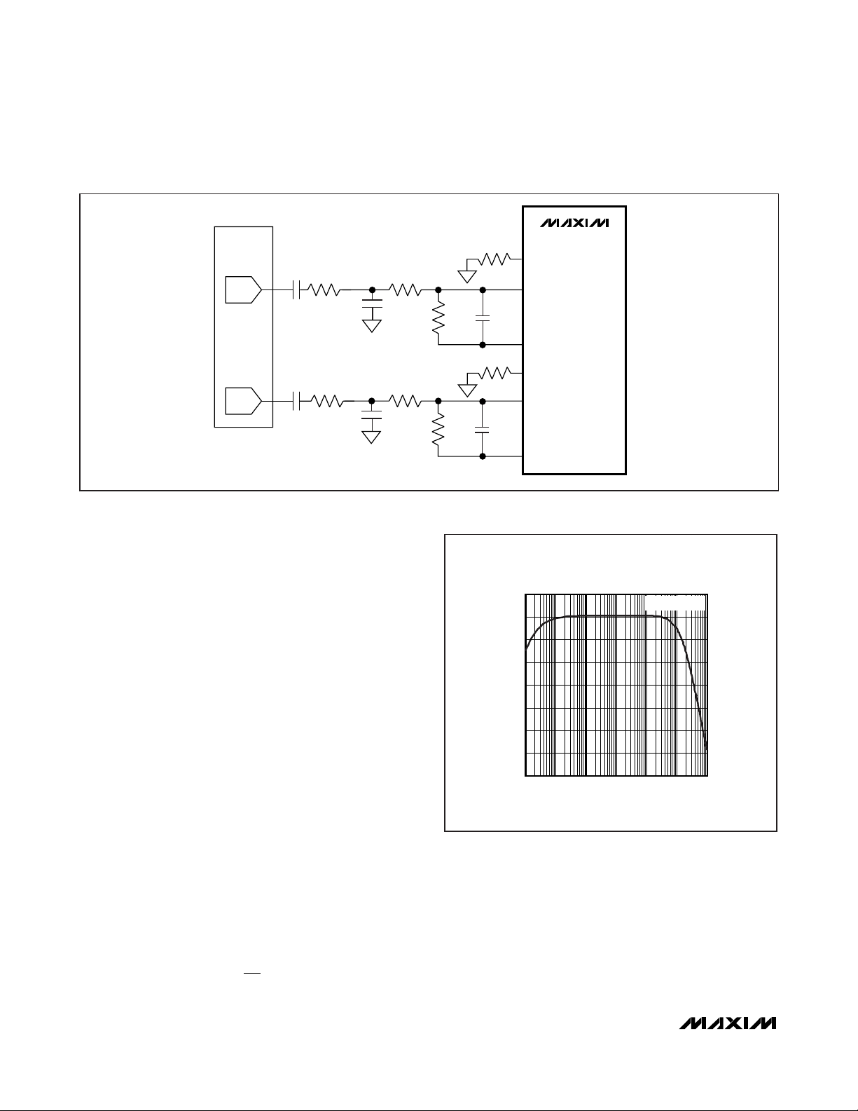
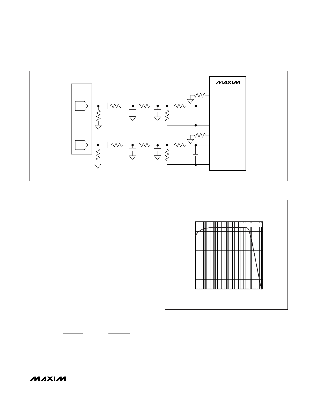
Lowpass Filter Configuration
for PCM1742 and CS4334
The lowpass filter configurations shown in Figures 13
and 15 are recommended when connecting a stereo
audio DAC to the audio preamplifier (input amplifier) of
the MAX9597. The filter configuration helps eliminate
the switching noise caused by the audio DAC. The corner frequency of the filter configuration should be set
above the maximum audio frequency (20kHz) and
below the sampling frequency of the DAC. The frequency response of the filter configurations is shown in
Figures 14 and 16.
Differential to Single-Ended Conversion
of Audio Signals
If the stereo audio DAC generates an analog, voltage
mode, differential audio signal, the circuit shown in Figure
17 can be used to convert the signal to single ended.
The gain of the circuit is represented by this equation:
Figure 13. Lowpass Filter Configuration for the Burr-Brown PCM1742
Figure 14. Filter Response of PCM1742 Filter Configuration
PCM1742
DAC
10μF
LEFT
604Ω
1.2nF
10μF
RIGHT
NOTE: ALL RESISTORS ARE 1%.
R
2
⎛
GAIN
⎞
=
×
⎜
⎟
⎝
⎠
R
1
604Ω
1.2nF
4
6.04kΩ
3.01kΩ
6.04kΩ
3.01kΩ
3.01kΩ
390pF
3.01kΩ
390pF
PCM1742 APPLICATION CIRCUIT WITHOUT THE DAC
10
5
0
-5
-10
GAIN (dB)
-15
-20
-25
-30
MAX9597
ENC_INL+
ENC_INL-
ENC_INLOUT
ENC_INR+
ENC_INR-
ENC_INROUT
FILTER RESPONSE vs. FREQUENCY
VIN = 0.25V
100k10k1k1001011M
FREQUENCY (Hz)
RMS
Page 23
MAX9597
Low-Power Audio/Video Interface
for Single SCART Connectors
______________________________________________________________________________________ 23
Keep the full-scale audio output of the preamplifiers to
0.5V
RMS
. Capacitors C1 and C2 create a one-pole,
lowpass filter to attenuate any high-frequency noise
coming from the stereo audio DAC. The frequency of
the lowpass pole is represented by this equation:
If the stereo audio DAC generates an analog, current
mode, and differential audio signal, the
Typical
Application Circuit
can be used to convert the signal to
single ended. The transresistance of the circuit is represented by this equation:
V
OUT
= I
DIFF
x R
F
Keep the full-scale audio output of the preamplifiers to
0.5V
RMS
. Capacitors C1 and C2 create a one-pole,
lowpass filter to attenuate any high-frequency noise
coming from the stereo audio DAC. The frequency of
the lowpass pole is represented by this equation:
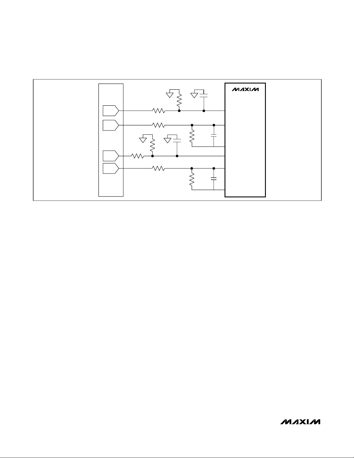
Figure 15. Lowpass Filter Configuration for the Cirrus CS4334
Figure 16. Filter Response of CS4334 Filter Configuration
CS4334
DAC
10μF
270kΩ
10μF
270kΩ
1.21kΩ
2.7nF
1.21kΩ
2.7nF
LEFT
RIGHT
NOTE: ALL RESISTORS ARE 1%.
4.64kΩ
3.3nF
4.64kΩ
3.3nF
f
=
dB dB−−
33
1
12
RR
×
⎛
2
ππ
⎜
⎝
12
RR
+
or f
⎞
1
C
⎟
⎠
=
2
1
RR
×
1
R
⎛
⎜
⎝
RR
12
+
2
⎞
C
2
⎟
⎠
3.57kΩ
1.21kΩ
2.40kΩ
1.21kΩ
2.40kΩ
560pF
3.57kΩ
560pF
FILTER RESPONSE vs. FREQUENCY
CS4334 APPLICATION CIRCUIT WITHOUT THE DAC
10
0
-10
-20
MAX9597
ENC_INL+
ENC_INL-
ENC_INLOUT
ENC_INR+
ENC_INR-
ENC_INROUT
VIN = 0.25V
RMS
f
dB
−−
33
1
RC
F
or f
dB
==
21
1
RC
22ππ() ()
F
GAIN (dB)
-30
-40
-50
-60
FREQUENCY (Hz)
100k10k1k1001011M
Page 24
MAX9597
Low-Power Audio/Video Interface
for Single SCART Connectors
24 ______________________________________________________________________________________
Stand-Alone Operational
Amplifier Applications
The input amplifier of the audio section can be utilized
for stand-alone operational amplifier applications by
configuring ENC_INR+ and ENC_INL+ input as the
noninverting input, ENC_INR- and ENC_INL- input as
the inverting input and ENC_INROUT and
ENC_INLOUT output as the output of the stand-alone
operational amplifier. The gain-bandwidth product of
the amplifier is 7MHz (typ).
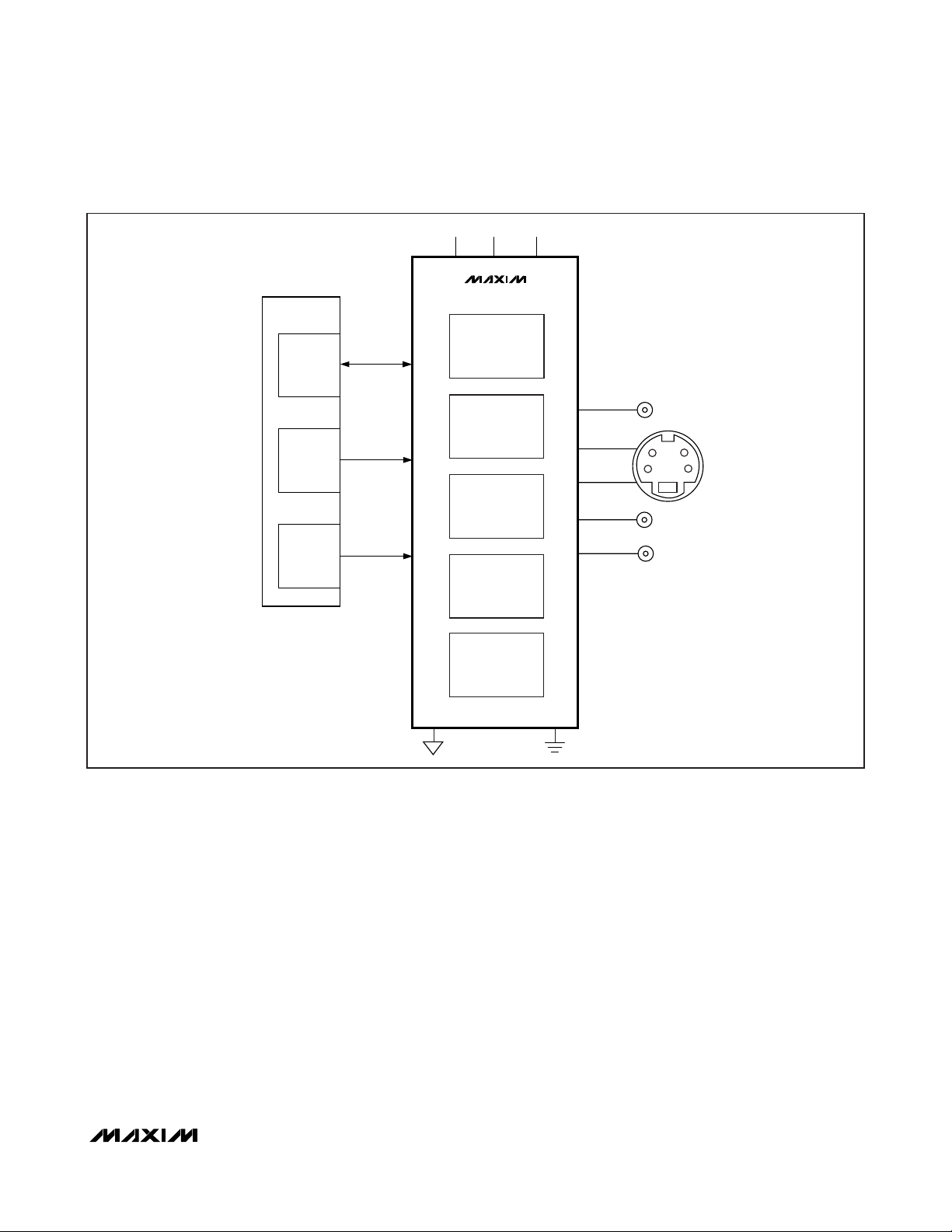
Applications That Do Not Need
the Slow-Switch Signal
V12should be left unconnected if the MAX9597 is used
in an application that does not require the slowswitch output signal. See Figure 18.
Power-Supply Bypassing
The MAX9597 features single 3.3V and 12V supply
operation and requires no negative supply. The 12V
supply V12is for the SCART slow-switching function.
For pin V12, place a 0.1μF bypass capacitor as close to
it as possible. Connect V
AUD
to 3.3V and bypass with a
10μF electrolytic capacitor in parallel with a 0.1μF
ceramic capacitor to audio ground. Bypass V
VID
to
GND with a 0.1μF ceramic capacitor.
Using a Digital Supply
The MAX9597 was designed to operate from noisy digital supplies. The high video PSRR (47dB at 100kHz)
allows the MAX9597 to reject the noise from the digital
power supplies (see the
Typical Operating Character-
istics
). If the digital power supply is very noisy and
stripes appear on the television screen, increase the
supply bypass capacitance. An additional, smaller
capacitor in parallel with the main bypass capacitor
can reduce digital supply noise because the smaller
capacitor has lower equivalent series resistance (ESR)
and equivalent series inductance (ESL).
Layout and Grounding
For optimal performance, use controlled-impedance
traces for video signal paths and place input termination resistors and output back-termination resistors
close to the MAX9597. Avoid routing video traces parallel to high-speed data lines.
Figure 17. Differential to Single-Ended Conversion Circuit for Voltage Mode, Differential Audio Signals
STB CHIP
LEFT_P
R1
LEFT_N
R2
R2
RIGHT_P
R1
RIGHT_N
R1
R2
C1
C1
ENC_INL+
ENC_INL-
R2
R2
C2
ENC_INLOUT
ENC_INR+
ENC_INR-
C2
ENC_INROUT
MAX9597
Page 25
MAX9597
Low-Power Audio/Video Interface
for Single SCART Connectors
______________________________________________________________________________________ 25
The MAX9597 provides separate ground connections
for video and audio supplies. For best performance,
use separate ground planes for each of the ground
returns and connect all ground planes together at a single point. Refer to the MAX9597 Evaluation Kit for a
proven circuit board layout example.
If the MAX9597 is mounted using flow soldering or
wave soldering, the ground via(s) for the exposed pad
should have a finished hole size of at least 14mil to
ensure adequate wicking of soldering onto the exposed
pad. If the MAX9597 is mounted using the solder mask
technique, the via requirement does not apply. In either
case, a good connection between the exposed pad
and ground is required to minimize noise from coupling
onto the outputs.
Figure 18. Set-Top Box with CVBS Output, S-Video Output, and Stereo Audio Outputs
STB CHIP
μC
VIDEO
ENCODER
STEREO
AUDIO
DAC
2
C
I
CVBS, Y/C
SINGLE OR
DIFFERENTIAL
STEREO AUDIO
V
12
N.C.
I2C INTERFACE
AND REGISTERS
VIDEO FILTERS
WITH DirectDrive
SLOW SWITCHING
FAST SWITCHING
CHARGE PUMP
V
ID
MAX9597
AUDIO
OUTPUTS
V
AUD
3.3V3.3V
CVBS
Y
C
LEFT AUDIO
RIGHT AUDIO
3
4
1
2
EP
GND
Page 26

MAX9597
Low-Power Audio/Video Interface
for Single SCART Connectors
26 ______________________________________________________________________________________
Table 7. Data Format for Write Mode
Register Tables
REGISTER
ADDRESS
(HEXADECIMAL)
BIT 7 BIT 6 BIT 5 BIT 4 BIT 3 BIT 2 BIT 1 BIT 0
0x00 Not used ZCD Not used
0x01 Not used
0x02 Not used
0x03 Not used
0x04 Not used
0x05 Not used
0x06 Not used
0x07 Not used
0x08 Not used
0x09 Not used
0x0A Not used
0x0B Not used
0x0C Not used
0x0D Not used
0x10
Operating
mode
Not
used
Not
used
Not
used
Not
used
TV audio
mute
Not used Set TV fast switching Not used Set TV slow switching
Not used Not used
TV_B_OUT TV_G_OUT TV_R/C_OUT TV_CVBS_OUT TV_FS_OUT
Not used Not used Not used Not used Not used
ENC_R/C_IN
clamp
Not used Not used
Not
used
Not
used
Not
used
Page 27

MAX9597
Low-Power Audio/Video Interface
for Single SCART Connectors
______________________________________________________________________________________ 27
Table 8. Register 00h: Audio Control
Table 9. Register 07h: TV Video Output Control
Table 10. Register 08h: VCR Video Input Control
DESCRIPTION
TV audio mute
Zero-crossing detector
76543210
——————— 0Off
——————— 1On (power-on default)
— 0 ——————Off
— 1 ——————On (power-on default)
BIT
DESCRIPTION
Set TV slow switching
Set TV fast switching
76543210
—————— 0 0
—————— 0 1
—————— 1 0High impedance
—————— 1 1
— — — 0 0 — — — GND (power-on default)
— — — 0 1 — — — Not used
— — — 1 0 — — — Same level as VCR_FB_IN
——— 1 1 ———V
BIT
COMMENTS
COMMENTS
Low (< 2V) internal source (power-on
default)
Medium (4.5V to 7V) external SCART
source with 16:9 aspect ratio
High ( > 9.5V) external SCART source
with 4:3 aspect ratio
VID
DESCRIPTION
ENC_R/C_IN clamp/bias
76543210
———— 0 ———
———— 1 ———Chrominance bias applied at input
BIT
COMMENTS
DC restore clamp active at input
(power-on default)
Page 28

MAX9597
Low-Power Audio/Video Interface
for Single SCART Connectors
28 ______________________________________________________________________________________
Table 11. Register 0Dh: Output Enable
Table 12. Register 10h: Operating Modes
MAX9597
TOP VIEW
26
27
25
24
10
9
11
C1P
CPVSS
DEV_ADDR
SDA
SCL
12
V
AUD
TV_SS_OUT
TV_B_OUT
TV_G_OUT
TV_OUTL
TV_R/C_OUT
GND
12
ENC_INROUT
4567
2021 19 17 16 15
ENC_INR-
ENC_INR+
TV_CVBS_OUT
ENC_CVBS_IN
ENC_R/C_IN
ENC_G_IN
C1N
V
12
3
18
28
8
TV_OUTR
ENC_B_IN
ENC_INLOUT
23
13
V
VID
ENC_INL-
22
14
TV_FS_OUT
ENC_INL+
+
EP*
*EXPOSED PAD. CONNECT EP TO AUDIO GROUND FOR
PROPER THERMAL AND ELECTRICAL PERFORMANCE
Pin Configuration
Chip Information
PROCESS: BiCMOS
DESCRIPTION
TV_FS_OUT enable
TV_CVBS_OUT enable
TV_B_OUT enable
TV_G_OUT enable
TV_R/C_OUT enable
76543210
—————— 0 —Off (power-on default)
—————— 1 —On
————— 0 ——Off (power-on default)
————— 1 ——On
———— 0 ———Off (power-on default)
———— 1 ———On
— — — 0 — — — — Off (power-on default)
——— 1 ————On
— — 0 — — — — — Off (power-on default)
—— 1 —————On
DESCRIPTION
Operating mode
76543210
0 ———————Shutdown
1 ———————Full-power mode (power-on default)
BIT
BIT
COMMENTS
COMMENTS
Page 29

MAX9597
Low-Power Audio/Video Interface
for Single SCART Connectors
______________________________________________________________________________________ 29
Typical Application Circuit
STB CHIP
μC
VIDEO
ENCODER
75Ω
75Ω
75Ω
+3.3V
12V
V
12
SDA
SCL
DEV_ADDR
ENC_CVBS_IN
ENC_R/C_IN
ENC_G_IN
0.1μF
3.3V
V
VID
MAX9597
3.3V
0.1μF
V
TV_OUTR
TV_OUTL
TV_SS_OUT
TV_B_OUT
TV_G_OUT
TV_R/C_OUT
TV_FS_OUT
TV_CVBS_OUT
0.1μF
AUD
C1P
300Ω
300Ω
100Ω
75Ω
75Ω
75Ω
75Ω
75Ω
TV
SCART
C1N
CPVSS
GND
EP
75Ω
124Ω
15nF
)
(R
(C1)
F
STEREO
AUDIO
CURRENT
DACS WITH
DIFFERENTIAL
OUTPUTS
NOTE: OPTIONAL RESISTOR CAN BE PLACED
FROM AUDIO DAC OUTPUTS TO GROUND TO
DECREASE SWING AT AUDIO DAC OUTPUTS.
124Ω
124Ω
124Ω
15nF
)
(R
(C2)
F
15nF
)
(R
(C1)
F
15nF
)
(C2)
(R
F
ENC_B_IN
ENC_INL+
ENC_INL-
ENC_INLOUT
ENC_INR+
ENC_INR-
ENC_INROUT
Page 30

MAX9597
Low-Power Audio/Video Interface
for Single SCART Connectors
30 ______________________________________________________________________________________
Package Information
For the latest package outline information and land patterns, go to www.maxim-ic.com/packages.
PACKAGE TYPE PACKAGE CODE DOCUMENT NO.
28 TQFN-EP T2855-8
21-0140
QFN THIN.EPS
Page 31

MAX9597
Low-Power Audio/Video Interface
for Single SCART Connectors
______________________________________________________________________________________ 31
Package Information (continued)
For the latest package outline information and land patterns, go to www.maxim-ic.com/packages.
Page 32

MAX9597
Low-Power Audio/Video Interface
for Single SCART Connectors
Maxim cannot assume responsibility for use of any circuitry other than circuitry entirely embodied in a Maxim product. No circuit patent licenses are
implied. Maxim reserves the right to change the circuitry and specifications without notice at any time.
32
____________________Maxim Integrated Products, 120 San Gabriel Drive, Sunnyvale, CA 94086 408-737-7600
© 2008 Maxim Integrated Products is a registered trademark of Maxim Integrated Products, Inc.
Revision History
REVISION
NUMBER
0 6/08 Initial release —
1 10/08 Corrected resistor value in Figure 13 22
REVISION DATE DESCRIPTION PAGES CHANGED
 Loading...