

Page 1
General Description
The MAX9595 dual SCART switch matrix routes audio
and video signals between an MPEG encoder and two
external SCART connectors under I2C†control, and
meets the requirements of EN50049-1, IEC 933-1,
Canal+, and BSkyB standards.
The video and audio channels feature input source
selection multiplexers, input buffers, and output buffers
for routing all inputs to selected outputs.
The MAX9595 provides programmable gain control from
+5dB to +7dB in 1dB steps for red, green, and blue component video signals. All other video outputs have a fixed
+6dB gain. Additional features include an internal luma
and chroma (Y/C) mixer that generates a composite
video signal (CVBS) to supply an RF modulator output,
and internal video reconstruction lowpass filters with a
cutoff frequency of 6MHz. The MAX9595 TV audio channel features clickless switching and programmable volume control from -56dB to +6dB in 2dB steps. The VCR
audio output also has programmable gain for -6dB, 0dB,
or +6dB. The device also generates monaural audio from
left and right stereo inputs. All audio drivers deliver a
3.0V
RMS
minimum output.
The MAX9595 operates with standard 5V and 12V
power supplies and supports slow-switching and fastswitching signals. The I2C interface programs the
gain and volume control, and selects the input source
for routing.
The MAX9595 is available in a compact 48-pin thin
QFN package and is specified over the 0°C to +70°C
commercial temperature range.
Applications
Satellite Set-Top Boxes
Cable Set-Top Boxes
TVs
VCRs
DVDs
Features
♦ Video Outputs Drive 2V
P-P
into 150Ω
♦ Audio Outputs Drive 3V
RMS
into 10kΩ
♦ Clickless, Popless Audio Gain Control and
Switching
♦ Interrupt Output Detects Changes on Slow
Switching Input
♦ AC-Coupled Video Inputs with Internal Clamp and
Bias
♦ DC-Coupled Video Outputs
♦ Composite Video Signal Created Internally from
Y/C Inputs
♦ Internal Video Reconstruction Filters Provide
-50dB at 27MHz
♦ Single-Ended Audio Input
♦ Red/Chroma Switch for Bidirectional I/O
♦ I
2
C-Programmable RGB Gain from +5dB to +7dB
♦ I
2
C-Programmable Audio Gain Control from +6dB
to -56dB
♦ Meets EN50049-1, IEC 933-1, Canal+, and BSkyB
Requirements
MAX9595
Audio/Video Switch for Dual SCART Connector
________________________________________________________________ Maxim Integrated Products 1
Ordering Information
19-3946; Rev 0; 1/06
For pricing, delivery, and ordering information, please contact Maxim/Dallas Direct! at
1-888-629-4642, or visit Maxim’s website at www.maxim-ic.com.
Pin Configuration and Typical Application Circuit appear at
end of data sheet.
System Block Diagram appears at end of data sheet.
EVALUATION KIT
AVAILABLE
†
Purchase of I
2
C components from Maxim Integrated Products,
Inc. or one of its sublicensed Associated Companies, conveys
a license under the Philips I
2
C Patent Rights to use these com-
ponents in an I
2
C system, provided that the system conforms to
the I
2
C Standard Specification as defined by Philips.
PART
TEMP RANGE
PINPACKAGE
PKG
CODE
MAX9595CTM+
(7mm x 7mm)
T4877-6
*EP = Exposed paddle.
+Denotes lead-free package.
0°C to +70°C
48 Thin QFN-EP*
Page 2
MAX9595
Audio/Video Switch for Dual SCART Connector
2 _______________________________________________________________________________________
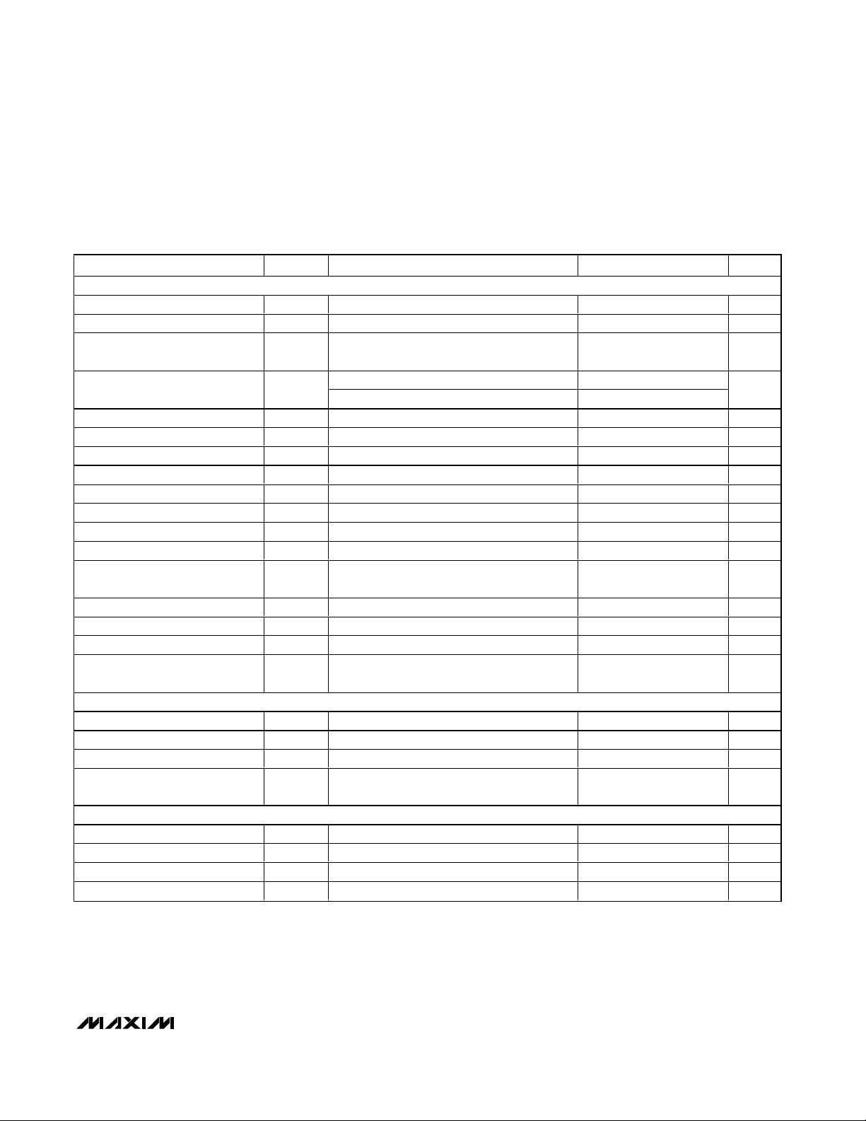
ABSOLUTE MAXIMUM RATINGS
ELECTRICAL CHARACTERISTICS
(V12= 12V, V
VID
= V
AUD
= 5V; 0.1µF X5R capacitor in parallel with a 10µF aluminum electrolytic capacitor from V
AUD
to GNDAUD,
V
12
to GNDAUD, and V
VID
to GNDVID; SET = 100kΩ nominal, R
LOAD
= 150Ω, TA= 0°C to +70°C, unless otherwise noted. Typical
values are at T
A
= +25°C.) (Note 1)
Stresses beyond those listed under “Absolute Maximum Ratings” may cause permanent damage to the device. These are stress ratings only, and functional
operation of the device at these or any other conditions beyond those indicated in the operational sections of the specifications is not implied. Exposure to
absolute maximum rating conditions for extended periods may affect device reliability.
V
VID
to GNDVID........................................................-0.3V to +6V
V
12
to GNDAUD .....................................................-0.3V to +14V
V
AUD
to GNDAUD ....................................................-0.3V to +6V
GNDAUD to GNDVID ............................................-0.1V to +0.1V
All Video Inputs, ENCIN_FS, VCRIN_FS,
SET to GNDVID......................................-0.3V to (V
VID
+ 0.3V)
All Audio Inputs,
AUDBIAS to GNDAUD .........................-0.3V to (V
AUD
+ 0.3V)
SDA, SCL, DEV_ADDR,
INTERRUPT_OUT to GNDVID ..............................-0.3V to +6V
All Audio Outputs, TV_SS,
VCR_SS to GNDAUD...............................-0.3V to (V
12
+ 0.3V)
INTERRUPT_OUT Current ................................................+50mA
All Video Outputs, TVOUT_FS to V
VID
, V
AUD
,
GNDAUD, GNDVID ................................................Continuous
All Audio Outputs to V
VID
, V
AUD
, V12,
GNDVID, GNDAUD ................................................Continuous
Continuous Power Dissipation (T
A
= +70°C)
48-Pin Thin QFN (derate 27mW/°C above +70°C) .....2105.3mW
Operating Temperature Range...............................0°C to +70°C
Junction Temperature......................................................+150°C
Storage Temperature Range .............................-65°C to +150°C
Lead Temperature (soldering, 10s) .................................+300°C
PARAMETER
CONDITIONS
UNITS
V
VID
Supply Voltage Range V
VID
Inferred from video gain test
5.0
V
AUD
Supply Voltage Range V
AUD
Inferred from audio gain test
5.0
V12 Supply Voltage Range V
12
Inferred from slow switching levels
V
V
VID
Quiescent Supply Current I
VID_Q
All video output amplifiers are enabled,
no load
69 100 mA
V
VID
Standby Supply Current I
VID_Q
All video output amplifiers are in shutdown,
and TV_FS_OUT driver is in shutdown, no
load
40 60 mA
V
AUD
Quiescent Supply Current
No load 2.4 6 mA
V12 Quiescent Supply Current I
12_Q
No load 3.6 6 mA
VIDEO CHARACTERISTICS
CVBS and Y-C, 1V
P-P
input
Voltage Gain G_V
RGB, 1V
P-P
input, (programmable gain
control)
dB
LP Filter Attenuation ATTN TA = +25°C, f = 6MHz, VIN = 1V
P-P
1.2 3.3 dB
LP Filter Suppression SPPR TA = +25°C, f = 27MHz, VIN = 1V
P-P
35 50 dB
Slew Rate SR V
OUT
= 2V
P-P
8 V/µs
Settling Time t
S
V
OUT
= 2V
P-P
, settle to 0.1% (Note 2)
ns
Gain Matching AG 1V
P-P
input, between RGB or Y-C
dB
Differential Gain DG 5-step modulated staircase 0.4 %
Differential Phase DP 5-step modulated staircase 0.2
degrees
SYMBOL
MIN TYP MAX
4.75
4.75
5.25
5.25
11.4 12.0 12.6
I
AUD_Q
+5.5 +6.0 +6.5
+4.5 +5.0 +5.5
+5.5 +6.0 +6.5
+6.5 +7.0 +7.5
380
-0.5 +0.5
Page 3
MAX9595
Audio/Video Switch for Dual SCART Connector
_______________________________________________________________________________________ 3
ELECTRICAL CHARACTERISTICS (continued)
(V12= 12V, V
VID
= V
AUD
= 5V; 0.1µF X5R capacitor in parallel with a 10µF aluminum electrolytic capacitor from V
AUD
to GNDAUD,
V
12
to GNDAUD, and V
VID
to GNDVID; SET = 100kΩ nominal, R
LOAD
= 150Ω, TA= 0°C to +70°C, unless otherwise noted. Typical
values are at T
A
= +25°C.) (Note 1)
PARAMETER
CONDITIONS
UNITS
Signal-to-RMS Noise
V
IN
= 1V
P-P
65 dB
Group Delay Variation ΔGD f = 0.1MHz to 4.43MHz 14 ns
Sync-Tip Clamp Level
RGB, composite, and luma input, no signal,
no load
V
Chroma Bias
Chroma input only, no signal, no load 1.9 V
Droop D Set by input current -2 +2 %
Power-Supply Rejection Ratio
DC, 0.5V
P-P
48 dB
CVBS or RGB video inputs, VIN > V_CLMP 4 MΩ
Input Impedance Z
IN
Chroma video input. VIN = V_BIAS 11 kΩ
Input Clamp Current I
CLMPVIN
= 1.75V 2.5 5 8.0 µA
Pulldown Resistance RP
Enable VCR_R/C_OUT and TV_R/C_OUT
pulldown through I
2
C, (see registers 7 and 9
for loading register details)
10 Ω
RGB, composite, and luma, no signal,
no load
Output Pin Bias Voltage V
OUT
Chroma, no signal, no load
V
Crosstalk XTLK
Between any two active inputs, f = 4.43MHz,
V
IN
= 1V
P-P
-50 dB
Mute Suppression
-50 dB
AUDIO CHARACTERISTICS (Note 3)
TV or VCR to stereo, gain = 0dB,
V
IN
= 1V
P-P
0
2.5 3.0 3.5
ENC to stereo, gain = 0dB, VIN = 1V
P-P
Voltage Gain (Measured From
Application Input)
G_A
ENC to mono, gain = 0dB, V
IN
= 1V
P-P
dB
Gain Matching Between
Channels
ΔG_A Gain = 0dB, V
IN
= 1V
P-P
0
dB
Flatness ΔA
f = 20Hz to 20kHz, 0.5V
RMS
input,
gain = 0dB
dB
Frequency Bandwidth BW
0.5V
RMS
input, frequency where output is
-3dB referenced to 1kHz
kHz
Input DC Level (Excluding
Encoder Inputs which are Hi-Z)
V
IN
Gain = 0dB
V
SYMBOL
MIN TYP MAX
SNR_V
V_CLMP
1.21
V_BIAS
PSRR_V
1.08
2.27
M_SPR_V f = 4.43MHz, VIN = 1V
, on one input only
P-P
TV or VCR to mono, gain = 0dB, VIN = 1V
-0.5
P-P
3.02 3.52 4.02
6.02 6.52 7.02
-0.5
0.01
230
0.2308
x V
12
+0.5
+0.5
Page 4
MAX9595
Audio/Video Switch for Dual SCART Connector
4 _______________________________________________________________________________________
ELECTRICAL CHARACTERISTICS (continued)
(V12= 12V, V
VID
= V
AUD
= 5V; 0.1µF X5R capacitor in parallel with a 10µF aluminum electrolytic capacitor from V
AUD
to GNDAUD,
V
12
to GNDAUD, and V
VID
to GNDVID; SET = 100kΩ nominal, R
LOAD
= 150Ω, TA= 0°C to +70°C, unless otherwise noted. Typical
values are at T
A
= +25°C.) (Note 1)
PARAMETER
CONDITIONS
UNIT
Single-ended inputs, f = 1kHz, THD < 1% 3
Input Signal Amplitude
(Measured from Application
Input)
ENC inputs single-ended, f = 1kHz,
THD < 1%
V
RMS
Single ended: VCR_INR, VCR_INL, TV_INR,
TV_INL
0.1
Input Resistance (Measured at
Parts Input)
R
IN
Encoder, ENC_INL, ENC_INR 0.1
MΩ
Output DC Level
VIN = 0V
0.5 x
V
12
V
Signal-to-Noise Ratio (Measured
from Application Input)
f = 1.0kHz, 1V
RMS
application input,
gain = 0dB, 20Hz to 20kHz
95 dB
R
LOAD
= 10kΩ, f = 1.0kHz, 0.5V
RMS
output
Total Harmonic Distortion Plus
Noise
R
LOAD
= 10kΩ, f = 1.0kHz, 2V
RMS
output
%
Output Impedance ZO f = 1kHz 1 Ω
1.414V
P-P
input, programmable gain to TV
SCART volume control range extends from
-56dB to +6dB
1.5 2 2.5
Volume Attenuation Step
1.414V
P-P
input, programmable gain to VCR
audio extends from -6dB to +6dB
5.5 6 6.5
dB
From V
12,
f = 1kHz, 0.5V
P-P
,
(C
AUD_BIAS
= 47µF), gain = 0dB
75
Power-Supply Rejection Ratio
From V
AUD
, f = 1kHz, 0.5V
P-P, VAUD
≥
+4.75V, V
AUD
≤ +5.25V, gain = 0dB
75
dB
Mute Suppression
f = 1kHz, 0.5V
RMS
input, set through I2C, see
register 1 for loading register details
90 dB
Audio Clipping Level VCLIP
f = 1kHz, 2.5V
RMS
input, gain = 6dB,
THD < 1%
3.6
V
RMS
Left-to-Right Crosstalk
f = 1kHz, 0.5V
RMS
input, gain = 0dB 80 dB
Crosstalk
TV SCART to VCR SCART or VCR SCART to
TV SCART, f = 1kHz, 0.5V
RMS
input, gain =
0dB
90 dB
SYMBOL
V
IN_AC
MIN TYP MAX
1.31
V
OUT_DC
SNR_A
0.004
0.004
THD+N
ASTEP
PSRR_A
M_SPR_A
XTLK_LR
XTLK_CC
Page 5
MAX9595
Audio/Video Switch for Dual SCART Connector
_______________________________________________________________________________________ 5
ELECTRICAL CHARACTERISTICS (continued)
(V12= 12V, V
VID
= V
AUD
= 5V; 0.1µF X5R capacitor in parallel with a 10µF aluminum electrolytic capacitor from V
AUD
to GNDAUD,
V
12
to GNDAUD, and V
VID
to GNDVID; SET = 100kΩ nominal, R
LOAD
= 150Ω, TA= 0°C to +70°C, unless otherwise noted. Typical
values are at T
A
= +25°C.) (Note 1)
PARAMETER
CONDITIONS
UNIT
DIGITAL INTERFACE: SDA and SCL (Note 4)
Low-Level Input Voltage V
IL
0 0.8 V
High-Level Input Voltage V
IH
2.6 V
Hysteresis of Schmitt Trigger
Input
0.2 V
I
SINK
= 3mA 0.4
SDA Low-Level Output Voltage V
OL
I
SINK
= 6mA 0.6
V
Output Fall Time for SDA Line 400pF bus load
ns
Spike Suppression 50 ns
Input Current -10
µA
Input Capacitance 5pF
SCL Clock Frequency 0
kHz
Hold Time
0.6 µs
Low Period of SCL Clock t
Low
1.3 µs
High Period of SCL Clock t
HIGH
0.6 µs
Setup Time for a Repeated Start
Condition
0.6 µs
Data Hold Time
0 0.9 µs
Data Setup Time
ns
Setup Time for Stop Condition
0.6 µs
Bus Free Time Between a Stop
and Start
t
BUF
1.3 µs
OTHER DIGITAL PINS (Note 4)
DEV_ADDR Low Level 0.8 V
DEV_ADDR High Level 2.6 V
INTERRUPT_OUT Low Voltage INTERRUPT_OUT sinking 1mA
0.4 V
INTERRUPT_OUT High Leakage
Current
V
INTERRUPT_OUT
= 5V 1 10 µA
SLOW SWITCHING SECTION (Note 4)
Input Low Level 02V
Input Medium Level 4.5 7.0 V
Input High Level 9.5 V
12
V
Input Current 50
µA
SYMBOL
t
HD,STA
t
SU,STA
t
HD,DAT
t
SU,DAT
t
SU,STO
MIN TYP MAX
100
0.15
250
+10
400
100
Page 6
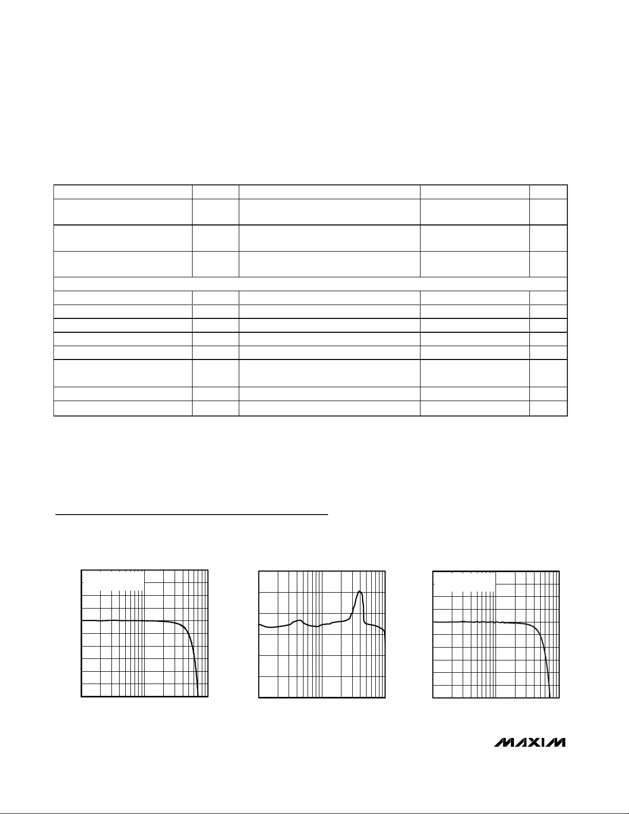
R/G/B VIDEO LARGE-SIGNAL BANDWIDTH
vs. FREQUENCY
MAX9595 toc01
FREQUENCY (MHz)
GAIN (dB)
1
-5
-4
-3
-2
-1
0
1
2
3
4
-6
0.1 10
VIN = 1V
P-P
RL = 150Ω TO GNDVID
GROUP DELAY vs. FREQUENCY
MAX9595 toc02
FREQUENCY (MHz)
GROUP DELAY (ns)
1
20
40
60
80
100
120
0
0.1 10
Y VIDEO LARGE-SIGNAL BANDWIDTH
vs. FREQUENCY
MAX9595 toc03
FREQUENCY (MHz)
GAIN (dB)
1
-5
-4
-3
-2
-1
0
1
2
3
4
-6
0.1 10
VIN = 1V
P-P
RL = 150Ω TO GNDVID
Typical Operating Characteristics
(V12= 12V, V
VID
= V
AUD
= 5V, 0.1µF X5R capacitor in parallel with a 10µF aluminum electrolytic capacitor from V
AUD
to GNDAUD,
V12to GNDAUD, V
VID
to GNDVID no load, TA= 0°C to +70°C, unless otherwise noted. Typical values are at TA = +25°C.)
MAX9595
Audio/Video Switch for Dual SCART Connector
6 _______________________________________________________________________________________
ELECTRICAL CHARACTERISTICS (continued)
(V12= 12V, V
VID
= V
AUD
= 5V; 0.1µF X5R capacitor in parallel with a 10µF aluminum electrolytic capacitor from V
AUD
to GNDAUD,
V
12
to GNDAUD, and V
VID
to GNDVID; SET = 100kΩ nominal, R
LOAD
= 150Ω, TA= 0°C to +70°C, unless otherwise noted. Typical
values are at T
A
= +25°C.) (Note 1)
PARAMETER
SYMBOL
CONDITIONS
MIN
TYP
MAX
UNIT
Output Low Level
10kΩ to ground, internal TV,
11.4 < V
12
< 12.6
0 1.5 V
Output Medium Level
10kΩ to ground, external 16/9,
11.4 < V
12
< 12.6
5 6.5 V
Output High Level
10kΩ to ground, external 4/3,
11.4 < V
12
< 12.6
10 V
12
V
FAST SWITCHING SECTION (Note 4)
Input Low Level 0 0.4 V
Input High Level 13V
Input Current 110µA
Output Low Level I
SINK
= 0.5mA 0
0.2 V
Output High Level I
SOURCE
= 20mA, V
VID
- V
OH
2V
Fast Switching Output to RGB
Skew
(Note 5) 30 ns
150Ω to ground 30 ns
Fast Switching Output Fall Time 150Ω to ground 30 ns
Note 1: All devices are 100% tested at TA= +25°C. All temperature limits are guaranteed by design.
Note 2: The settling time is measured from the 50% of the input swing to the 0.1% of the final value of the output.
Note 3: Maximum load capacitance is 200pF. All the listed parameters are measured at application’s inputs, unless otherwise
noted. See the Typical Application Circuits.
Note 4: Guaranteed by design.
Note 5: Difference in propagation delays of fast-blanking signal and RGB signals. Measured from 50% input transition to 50%
output transition. Signal levels to be determined.
0.01
0.75
Fast Switching Output Rise Time
Page 7
MAX9595
Audio/Video Switch for Dual SCART Connector
_______________________________________________________________________________________ 7
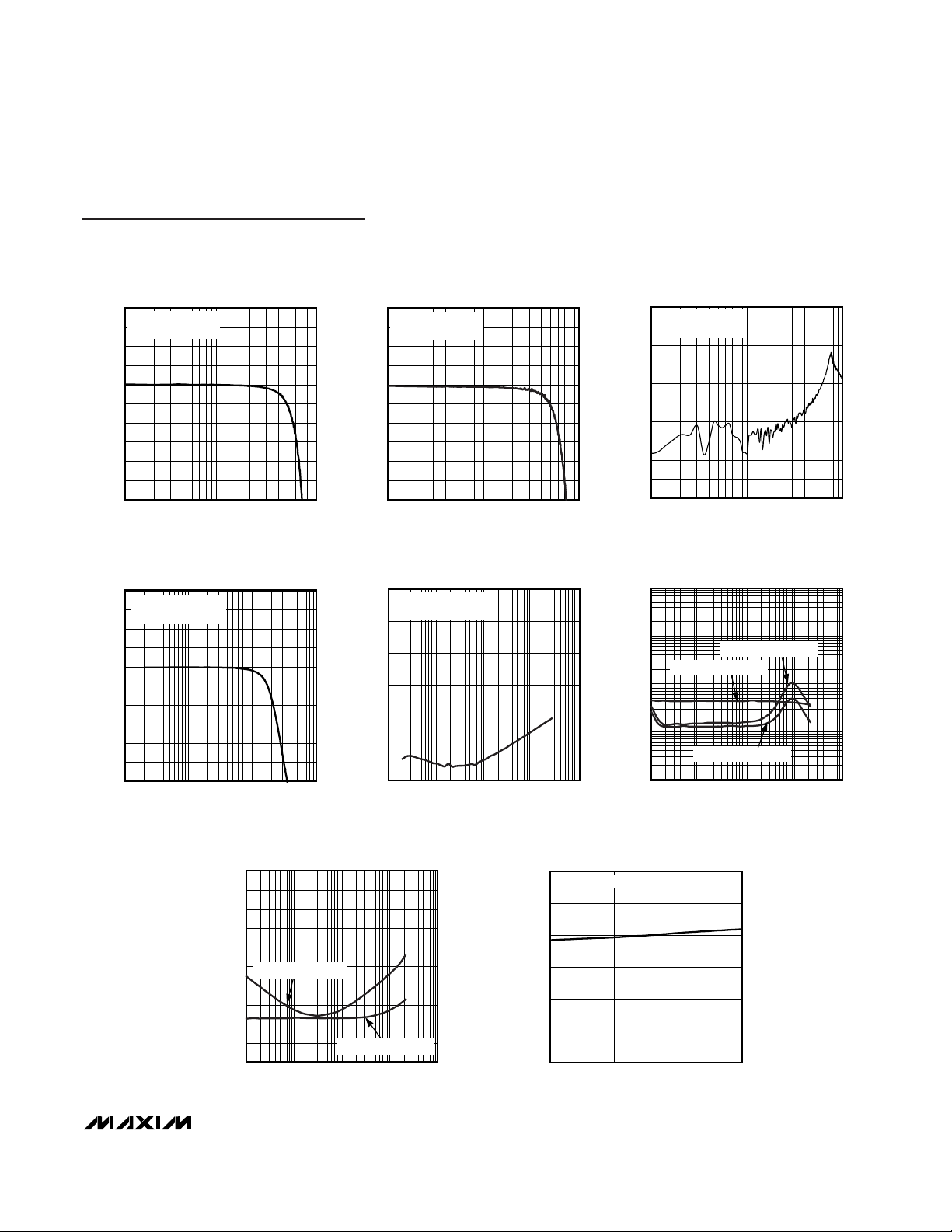
AUDIO CROSSTALK
vs. FREQUENCY
MAX9595 toc08
FREQUENCY (kHz)
CROSSTALK (dB)
100.1
-100
-80
-60
-40
-20
0
-120
0.01 100
VIN = 0.5V
RMS
RL = 10kΩ TO GNDAUD
1
AUDIO LARGE-SIGNAL BANDWIDTH
vs. FREQUENCY
MAX9595 toc07
FREQUENCY (kHz)
GAIN (dB)
10010
4
11000
3
2
1
0
-1
-2
-3
-4
-5
-6
VIN = 0.5V
RMS
RL = 10kΩ TO GNDAUD
AUDIO TOTAL HARMONIC DISTORTION
PLUS NOISE vs. FREQUENCY
MAX9595 toc09
FREQUENCY (kHz)
THD+N (%)
101
0.001
0.01
0.1
0
0.0001
0.01 100
AMPLITUDE = 3.0V
RMS
AMPLITUDE = 0.5V
RMS
AMPLITUDE = 2.0V
RMS
0.1
R/G/B VIDEO SMALL-SIGNAL BANDWIDTH
vs. FREQUENCY
MAX9595 toc04
FREQUENCY (MHz)
GAIN (dB)
1
-5
-4
-3
-2
-1
0
1
2
3
4
-6
0.1 10
VIN = 100mV
P-P
RL = 150Ω TO GNDVID
Y VIDEO SMALL-SIGNAL BANDWIDTH
vs. FREQUENCY
MAX9595 toc05
FREQUENCY (MHz)
GAIN (dB)
1
-5
-4
-3
-2
-1
0
1
2
3
4
-6
0.1 10
VIN = 100mV
P-P
RL = 150Ω TO GNDVID
VIDEO CROSSTALK vs. FREQUENCY
MAX9595 toc06
FREQUENCY (MHz)
CROSSTALK (dB)
1
-90
-80
-70
-60
-50
-40
-30
-20
-10
0
-100
0.1 10
VIN = 100mV
P-P
RL = 150Ω TO GNDVID
POWER-SUPPLY REJECTION RATIO
vs. FREQUENCY
MAX9595 toc10
FREQUENCY (kHz)
PSRR (dB)
1010.10.01 100
-90
-80
-70
-60
-50
-40
-30
-20
-10
-100
0
WITH RESPECT TO V
12
WITH RESPECT TO V
AUD
V
VID
QUIESCENT SUPPLY CURRENT
vs. TEMPERATURE
MAX9595 toc11
TEMPERATURE (°C)
V
VID
QUIESCENT SUPPLY CURRENT (mA)
5025
55
60
65
70
75
80
50
075
ALL VIDEO OUTPUT AMPLIFIERS ENABLED
NO LOAD
Typical Operating Characteristics (continued)
(V12= 12V, V
VID
= V
AUD
= 5V, 0.1µF X5R capacitor in parallel with a 10µF aluminum electrolytic capacitor from V
AUD
to GNDAUD,
V12to GNDAUD, V
VID
to GNDVID no load, TA= 0°C to +70°C, unless otherwise noted. Typical values are at TA = +25°C.)
Page 8
MAX9595
Audio/Video Switch for Dual SCART Connector
8 _______________________________________________________________________________________
Typical Operating Characteristics (continued)
(V12= 12V, V
VID
= V
AUD
= 5V, 0.1µF X5R capacitor in parallel with a 10µF aluminum electrolytic capacitor from V
AUD
to GNDAUD,
V12to GNDAUD, V
VID
to GNDVID no load, TA= 0°C to +70°C, unless otherwise noted. Typical values are at TA = +25°C.)
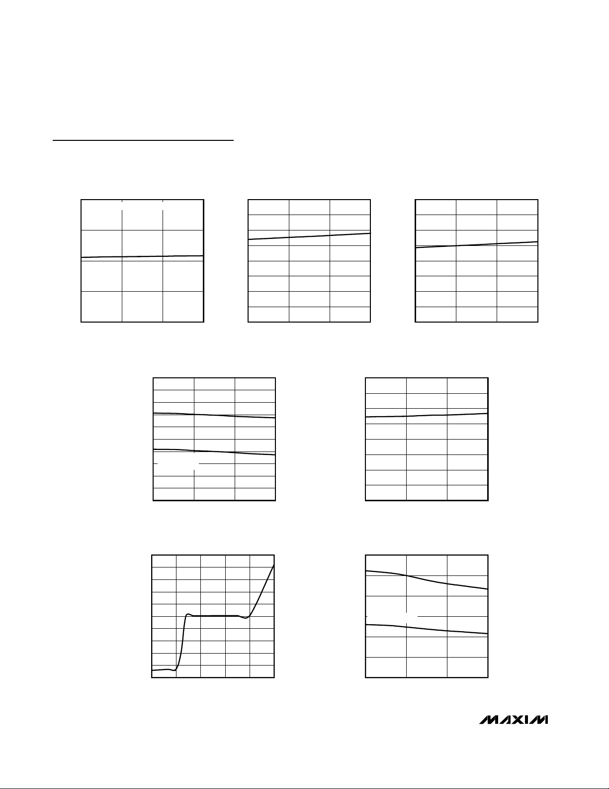
V
VID
STANDBY QUIESCENT SUPPLY
CURRENT vs. TEMPERATURE
MAX9595 toc12
TEMPERATURE (°C)
V
VID
STANDBY QUIESCENT SUPPLY CURRENT (mA)
5025
35
40
45
50
30
075
ALL VIDEO OUTPUT AMPLIFIERS DISABLED
V12 QUIESCENT SUPPLY CURRENT
vs. TEMPERATURE
MAX9595 toc13
TEMPERATURE (°C)
V
12
QUIESCENT SUPPLY CURRENT (mA)
5025075
1.5
2.0
2.5
3.0
3.5
4.0
4.5
5.0
1.0
V
AUD
QUIESCENT SUPPLY CURRENT
vs. TEMPERATURE
MAX9595 toc14
TEMPERATURE (°C)
V
AUD
QUIESCENT SUPPLY CURRENT (mA)
5025075
0.5
1.0
1.5
2.0
2.5
3.0
3.5
4.0
0
INPUT CLAMP AND BIAS LEVEL
vs. TEMPERATURE
MAX9595 toc15
TEMPERATURE (°C)
INPUT CLAMP AND BIAS LEVEL (V)
5025075
0.7
0.9
1.1
1.3
1.7
1.5
1.9
2.1
2.3
2.5
0.5
BOTTOM LEVEL
CLAMP
BIAS
INPUT CLAMP CURRENT
vs. TEMPERATURE
MAX9595 toc16
TEMPERATURE (°C)
INPUT CLAMP CURRENT (μA)
5025075
2.5
3.0
3.5
4.0
4.5
5.0
5.5
6.0
2.0
V
IN
= 1.75V
INPUT CLAMP CURRENT
vs. INPUT VOLTAGE
MAX9595 toc17
INPUT VOLTAGE (V)
INPUT CLAMP CURRENT (mA)
4321
-0.4
-0.3
-0.2
-0.1
0
0.1
0.2
0.3
0.4
0.5
-0.5
05
OUTPUT BIAS VOLTAGE
vs. TEMPERATURE
MAX9595 toc18
TEMPERATURE (°C)
OUTPUT BIAS VOLTAGE (V)
5025
0.5
1.0
1.5
2.0
2.5
3.0
0
075
CHROMA
RGB, LUMA, CVBS
Page 9
MAX9595
Audio/Video Switch for Dual SCART Connector
_______________________________________________________________________________________ 9
Pin Description
PIN NAME FUNCTION
1 SDA Bidirectional Data I/O. I2C -compatible, 2-wire interface data input/output. Output is open drain.
2 SCL Serial Clock Input. I2C -compatible, 2-wire clock interface.
3 DEV_ADDR
Device Address Set Input. Connect to GNDVID to set write and read addresses of 94h or 95h,
respectively. Connect to V
VID
to set write and read address of 96h or 97h, respectively.
4 ENC_INL Digital Encoder Left-Channel Audio Input
5
Interrupt Output. INTERRUPT_OUT is an open-drain output that goes high impedance to
indicate a change in the slow switch lines, TV_SS or VCR_SS.
6 ENC_INR Digital Encoder Right-Channel Audio Input
7 N.C. No Connection. Not internally connected.
8 VCR_INR VCR SCART Right-Channel Audio Input
9 VCR_INL VCR SCART Left-Channel Audio Input
10 TV_INR TV SCART Right-Channel Audio Input
11 TV_INL TV SCART Right-Channel Audio Input
12 GNDAUD Audio Ground
13 AUD_BIAS
Audio Input Bias Voltage. Bypass AUD_BIAS with a 47µF capacitor and a 0.1µF capacitor to
AUDGND.
14 V
AUD
Audio Supply. Connect to a +5V supply. Bypass with a 10µF aluminum electrolytic capacitor in
parallel with a 0.47µF low-ESR ceramic capacitor to GNDAUD.
15 VCR_OUTR VCR SCART Right-Channel Audio Output
16 VCR_OUTL VCR SCART Left-Channel Audio Output
17
RF Modulator Mono Audio Output
18 TV_OUTL TV SCART Left-Channel Audio Output
19 TV_OUTR TV SCART Right-Channel Audio Output
20 V
12
+12V Supply. Bypass V12 with a 10µF capacitor in parallel with a 0.1µF capacitor to ground.
21 TV_SS TV SCART Bidirectional Slow-Switch Signal
22 VCR_SS VCR SCART Bidirectional Slow-Switch Signal
23 SET Filter Cutoff Frequency Set Input. Connect 100kΩ resistor from SET to ground.
24, 36 V
VID
Video and Digital Supply. Connect to a +5V supply. Bypass with a 0.01µF capacitor to GNDVID.
V
VID
also serves as a digital supply for the I2C interface.
25 VCRIN_FS VCR SCART Fast-Switching Input
26 ENCIN_FS Digital Encoder Fast-Switching Input
27 TVOUT_FS
TV SCART Fast-Switching Output. This signal is used to switch the TV to its RGB inputs for onscreen display purposes.
28 GNDVID Video Ground
29 RF_CVBS_OUT RF Modulator Composite Video Output. Internally biased at 1V.
30
TV SCART Luma/Composite Video Output. Internally biased at 1V.
31 TV_R/C_OUT
TV SCART Red/Chroma Video Output. Internally biased at 1V for red video signal and 2.2V for
chroma video signal.
INTERRUPT_OUT
RF_MONO_OUT
TV_Y/CVBS_OUT
Page 10

MAX9595
Audio/Video Switch for Dual SCART Connector
10 ______________________________________________________________________________________
Pin Description (continued)
PIN NAME FUNCTION
32 TV_G_OUT TV SCART Green Video Output. Internally biased at 1V.
33 TV_B_OUT TV SCART Blue Video Output. Internally biased at 1V.
34
VCR SCART Luma/Composite Video Output. Internally biased at 1V.
35 VCR_R/C_OUT
VCR SCART Red/Chroma Video Output. Internally biased at 1V for red video signals and 2.2V
for chroma video signal.
37 TV_R/C_IN
TV SCART Red/Chroma Video Input. Internally biased at 1V for red video signals, or 2.2V for
chroma video signals.
38 TV_Y/CVBS_IN TV SCART Luma/Composite Video Input. Internally biased at 1.2V.
39
VCR SCART Luma/Composite Video Input. Internally biased at 1.2V.
40 VCR_R/C_IN
VCR SCART Red/Chroma Video Input. Internally biased at 1.2V for red video signals and 1.9V
for chroma video signals.
41 VCR_G_IN VCR SCART Green Video Input. Internally biased at 1.2V.
42 VCR_B_IN VCR SCART Blue Video Input. Internally biased at 1.2V.
43
Digital Encoder Luma/Composite Video Input. Internally biased at 1.2V.
44 ENC_R/C_IN
Digital Encoder Red/Chroma Video Input. Internally biased at 1.2V for red video signals, or 1.9V
for chroma video signals.
45 ENC_G_IN Digital Encoder Green Video Input. Internally biased at 1.2V.
46 ENC_B_IN Digital Encoder Blue Video Input. Internally biased at 1.2V.
47 ENC_Y_IN Digital Encoder Luma Video Input. Internally biased at 1.2V.
48 ENC_C_IN Digital Encoder Chroma Video Input. Internally biased at 1.9V.
EP GNDAUD
Exposed Paddle. Solder to the circuit board ground (GNDAUD) for proper thermal and electrical
performance.
Detailed Description
The MAX9595 is a switch matrix that routes audio and
video signals between different ports using the I2C
interface. The ports consist of the MPEG decoder output, and two SCART connectors for the TV and VCR.
Per EN50049 and IEC 933, the encoder can only input
a signal to the SCART connector, while TV and VCR
SCART connectors are bidirectional.
The MAX9595 circuitry consists of four major sections:
the video section, the audio section, the slow- and fastswitching section, and the digital interface.
The video section consists of clamp and bias circuitry,
input buffers, reconstruction filters, a switch matrix, a
Y/C mixer, and output buffers. All video inputs are ACcoupled through a 0.1µF capacitor to set an acceptable
DC level using clamp or bias networks. The bidirectional red/chroma outputs can be connected to ground
using I2C control to make them terminations when
red/chroma is an input (see the Video Inputs section).
The audio section features an input buffer, a switching
matrix, volume- or gain-control circuitry, and output drivers. The audio inputs are AC-coupled through a 0.1µF
capacitor. The TV output audio path has volume control
from -56dB to +6dB in 2dB steps, while the VCR output
audio path has volume control from -6dB to +6dB in
6dB steps. The MAX9595 can be configured to switch
inputs during a zero-crossing function to reduce clicks.
The slow-switching feature allows for bidirectional, trilevel, slow-switching input and output signals at pin
VCR_SS and TV_SS, respectively. The slow-switching
signals from the VCR set the aspect ratio or video source
of the TV screen. If INTERRUPT_OUT is enabled, then
INTERRUPT_OUT changes to a high-impedance state if
any of the slow-switching inputs change logic levels. See
the Slow Switching section.
VCR_Y/CVBS_OUT
VCR_Y/CVBS_IN
ENC_Y/CVBS_IN
Page 11

MAX9595
Audio/Video Switch for Dual SCART Connector
______________________________________________________________________________________ 11
Fast switching consists of two inputs from the encoder
and VCR, and one output to the TV to insert an onscreen display (OSD). Fast switching is used to route
video signals from the VCR or from the encoder to the
TV. In addition, the fast-switching output can be configured to a high or low voltage. Fast switching is controlled through the I2C interface.
The digital block contains the 2-wire interface circuitry,
control, and status registers. The MAX9595 can be
configured through an I2C-compatible interface.
DEV_ADDR sets the I2C-compatible address.
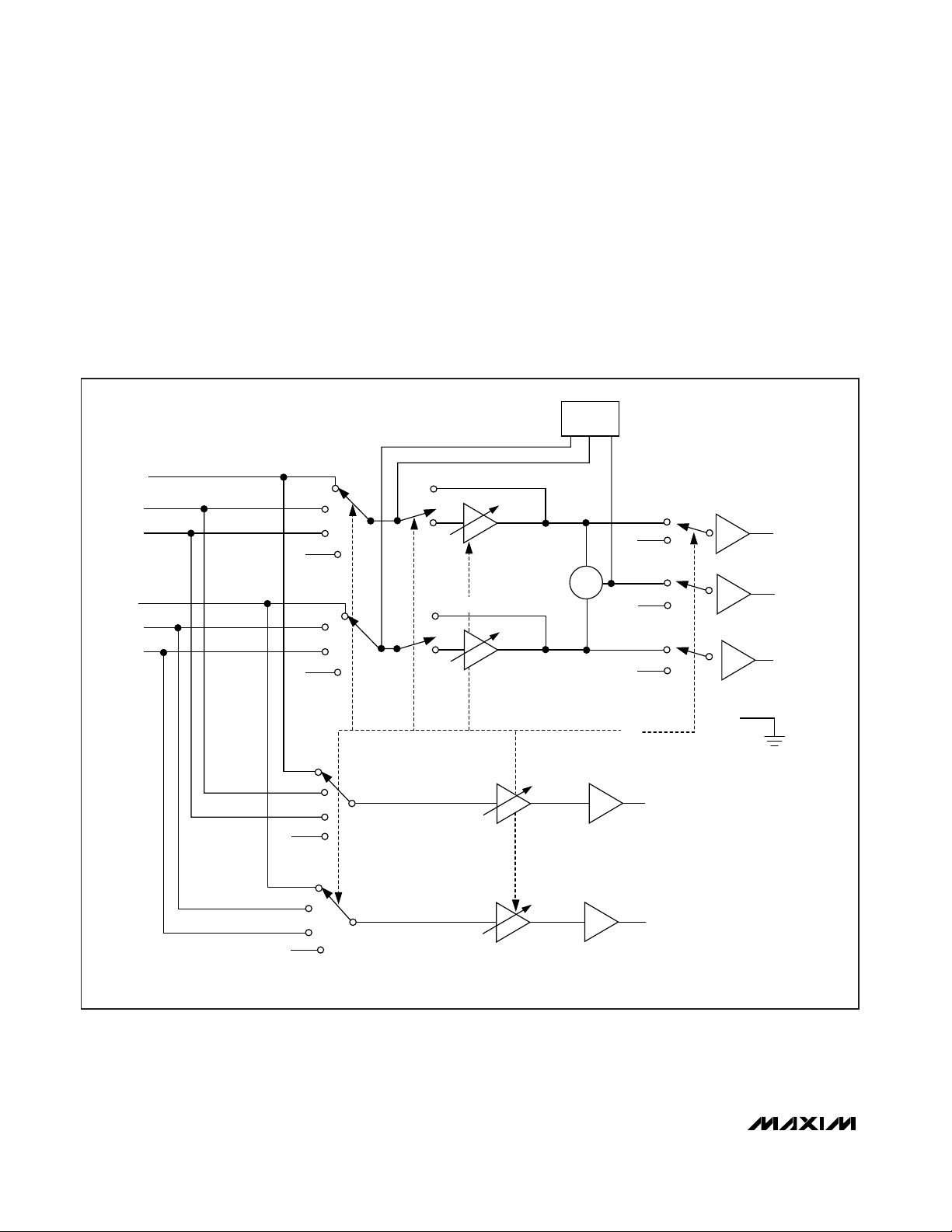
SCART Video Switching
The MAX9595 switches video signals between an MPEG
decoder, TV SCART, and VCR SCART. The video switch
includes reconstruction filters, multiplexed video amplifiers, and a Y-C mixer driver for an RF modulator. See
Figure 1 for the functional diagram of the video section.
While the SCART connector supports RGB, S-video, and
composite video formats, RGB, and S-video typically
share a bidirectional set of SCART connector pins.
CLAMP/BIAS
TV_R/C_IN
CLAMP
TV_Y/CVBS_IN
CLAMP
VCR_B_IN
CLAMP
VCR_G_IN
CLAMP/BIAS
VCR_R/C_IN
VCRIN_FS
CLAMP
ENC_Y/CVBS_IN
CLAMP/BIAS
ENC_R/C_IN
CLAMP
ENC_G_IN
CLAMP
ENC_B_IN
CLAMP
ENC_Y_IN
ENCIN_FS
BIAS
ENC_C_IN
0.7V
0.7V
2kΩ
2kΩ
V
12
VCR_Y/CVBS_OUT
VCR_R/C_OUT
TV_R/C_OUT
TV_G_OUT
TV_B_OUT
TV_Y/CVBS_OUT
TVOUT_FS
RF_CVBS_OUT
INTERRUPT_OUT
BIAS
5V
0V
PULLDOWN
TVRCOUT
VGA
5dB, 6dB, OR 7dB
PULLDOWN
VCRRCOUT
x2
x2
x2
x1
TV_SS
VCR_SS
x2
VGA
5dB, 6dB, OR 7dB
VGA
5dB, 6dB, OR 7dB
N
N
MAX9595
FILTER
FILTER
MIXER
FILTER
FILTER
FILTER
FILTER
SW/MONITOR
VCR_Y/CVBS_IN
CLAMP
Figure 1. MAX9595 Video Section Functional Diagram
Page 12

MAX9595
Video Inputs
All video inputs are AC-coupled with an external 0.1µF
capacitor. Either a clamp or bias circuit sets the DC
input level of the video signals. The clamp circuit positions the sync tip of the composite (CVBS), the component RGB, or the S-video luma signal. If the signal does
not have a sync tip, then the clamp positions the minimum of the signal at the clamp voltage. The bias circuitry is used to position the S-video chroma signal at
midlevel of the luma (Y) signal. On the video inputs that
can receive either a chroma or a red video signal, the
bias or clamp circuit is selected through I2C. See Tables
3–12 for loading register details.
The MPEG decoder and VCR uses the RGB format and
fast switching to insert an on-screen display (OSD), usually text, onto the TV. The MAX9595 supports RGB as an
input from either the VCR or the MPEG decoder and as
an output only to the TV. The red video signal of the
RGB format and the chroma video signal of the S-VHS
format share the same SCART connector pin. Therefore,
RGB and S-video signals cannot be present at the same
time. Loop-through is possible with a composite video
signal but not with RGB signals because the RGB
SCART pins are used for both input and output.
In SCART, there is the possibility of a bidirectional use
of the red/chroma pin. When using the red/chroma pin
as an input port, terminate the red/chroma output with a
75Ω resistor to ground. Thus, a ground state is provided by an active pulldown to GNDVID on the red/chroma
output to support the bidirectional chroma or red I/O,
turning the output source resistors into terminations
(see Figure 2). The active pulldown also provides the
“Mute Output” function, and disables the deselected
video outputs. The “Mute Output” state is the default
power-on state for video.
For high-quality home video, the MPEG decoder, VCR,
and TV use the S-video format. The MAX9595 supports
S-video signals as an input from the VCR, the MPEG
decoder, and the TV, and also as a separately switchable output to the TV and VCR. Because S-video support was not included in the original specifications of
the SCART connector, the luma (Y) signal of S-video
and the CVBS signal share the same SCART connector
pins. If S-video is present, then a composite signal
must be created from the Y and C signals to drive the
RF_CVBS_OUT pin. For S-video, loop-through is not
possible since the chroma SCART port is used for both
input and output.
The MAX9595 supports composite video (CVBS) format, with inputs from the VCR, MPEG decoder, and TV.
Full loop-through is possible to the TV and VCR only,
since the MPEG decoder SCART connector has separate input and output pins for the CVBS format.
Audio/Video Switch for Dual SCART Connector
12 ______________________________________________________________________________________
CLAMP
N
CLAMP/BIAS
TV_R/C_IN
VIDEO INPUT
TV_R/C_IN
VIDEO INPUT
75Ω
0.1μF
0.1μF
75Ω
PIN 15
PIN 13
PIN 15
PIN 13
MAX9595
MAX9595
TV_R/C_OUT
PULLDOWN
SCART
CABLE
SCART
CONNECTORS
PULLDOWN
CLAMP
N
TV_R/C_OUT
CLAMP/BIAS
Figure 2. Bidirectional SCART Pins
Page 13

Video Outputs
The DC level at the video outputs is controlled so that
coupling capacitors are not required, and all of the
video outputs are capable of driving a DC-coupled,
150Ω, back-terminated coax load with respect to
ground. Since some televisions and VCRs use the horizontal sync height for automatic gain control, the
MAX9595 accurately reproduces the sync height to
within ±2%.
Slow Switching
The MAX9595 supports the IEC 933-1, Amendment 1,
tri-level slow switching that selects the aspect ratio for
the display (TV). Under I
2
C-compatible control, the
MAX9595 sets the slow-switching output voltage level.
Table 1 shows the valid input levels of the slow-switching signal and the corresponding operating modes of
the display device.
Two bidirectional ports are available for slow-switching
signals for the TV and VCR. The slow-switching input
status is continuously read and stored in register 0Eh.
The slow-switching outputs can be set to a logic level
or high impedance by writing to registers 07h and 09h.
See Tables 8 and 10 for details. When enabled, INTERRUPT_OUT becomes high impedance if the voltage
level changes on TV_SS or VCR_SS.
Fast Switching
The VCR or MPEG decoder outputs a fast-switching
signal to the display device or TV to insert on-screen
display (OSD). The fast-switching signal can also be
set to a constant high or low output signal through the
I2C interface. The fast-switching output can be set
through writing to register 07h.
Y/C Mixer
The MAX9595 includes an on-chip mixer to produce
composite video (CVBS) when S-video (Y and C) is present. The composite video drives the RF_CVBS_OUT
output pin. The circuit sums Y and C signals to obtain the
CVBS component. A +6dB output buffer drives
RF_CVBS_OUT.
Video Reconstruction Filter
The encoder DAC outputs need to be lowpass-filtered
to reject the out-of-band noise. The MAX9595 integrates the reconstruction filter. The filter is fourth order,
which is composed of two Sallen-Key biquad in cascade, implementing a Butterworth-type transfer function. The internal reconstruction filters feature a 6MHz
cutoff frequency, and -35dB minimum attenuation at
27MHz. Note that the SET pin is used to set the accuracy of the filter cutoff frequency. Connect a 100kΩ resis-
tor from SET to ground.
SCART Audio Switching
Audio Inputs
The audio block has three stereo audio inputs from the
TV, the VCR, and the MPEG decoder SCART. Each input
has a 100kΩ resistor connected to an internally generated voltage equal to 0.23 x V
12
, and is AC-coupled.
MAX9595
Audio/Video Switch for Dual SCART Connector
______________________________________________________________________________________ 13
Table 1. Slow-Switching Modes
SLOW-SWITCHING
SIGNAL VOLTAGE
(V)
MODE
0 to 2
Display device uses an internal source
such as a built-in tuner to provide a
video signal
4.5 to 7.0
Display device uses a video signal from
the SCART connector and sets the
display to 16:9 aspect ratio
9.5 to 12.6
Display device uses a signal from the
SCART connector and sets the display
to 4:3 aspect ratio
Page 14
MAX9595
Audio Outputs
Both right and left channels have a stereo output for the
TV and VCR SCART. The monaural output, which is a
mix of the TV right and left channels, drives the RF
modulator, RF_MONO_OUT. The monaural mixer, a
resistor summer, attenuates the amplitude of each of
the two signals by 6dB. A 12.54dB gain block follows
the monaural mixer. If the left and right audio channels
were completely uncorrelated, then a 9.54dB gain
block is used. See Figure 3 for the functional diagram
of the audio section.
Clickless Switching
The TV channel incorporates a zero-crossing detect
(ZCD) circuit that minimizes click noise due to abrupt
signal level changes that occur when switching
between audio signals at an arbitrary moment.
Audio/Video Switch for Dual SCART Connector
14 ______________________________________________________________________________________
AUDIO INPUTS AUDIO OUTPUTS
ENC_INL
TV_INL
VCR_INL
MUTE
MUTE
MUTE
Σ/2
MUTE
MUTE
MUTE
MUTE
MUTE IS AN INTERNAL SIGNAL
-6dB, 0dB, OR +6dB
-6dB, 0dB, OR +6dB
9.54dB
9.54dB
12.54dB
GNDAUD
9.54dB
ZCD
TV_OUTL
RF_MONO_OUT
TV_OUTR
VOLUME CONTROL BYPASS
VOLUME CONTROL
+6dB TO -56dB
VOLUME CONTROL
+6dB TO -56dB
I
2
C
VCR_OUTL
VCR_OUTR
9.54dB
ENC_INR
TV_INR
VCR_INR
VOLUME CONTROL BYPASS
Figure 3. MAX9595 Audio Section Functional Diagram
Page 15

To implement the zero-crossing function when switching audio signals, set the ZCD bit by loading register
00h through the I2C-compatible interface (if the ZCD bit
is not already set). Then set the mute bit low by loading
register 00h. Next, wait for a sufficient period of time for
the audio signal to cross zero. This period is a function
of the audio signal path’s low-frequency 3dB corner
(f
L3dB
). Thus, if f
L3dB
= 1kHz, the time period to wait for
a zero-crossing detect is 0.5kHz or 0.5ms.
Next, set the appropriate TV switches using register
01h. Finally, clear the mute bit (while leaving the ZCD
bit high) using register 00h. The MAX9595 switches the
signal out of mute at the next zero crossing.
To implement the zero-cross function for TV volume
changes, or for TV and phono volume bypass switching, simply ensure the ZCD bit in register 00h is set.
Volume Control
The TV channel volume control ranges from -56dB to
+6dB in 2dB steps. The VCR volume control settings
are programmable for -6dB, 0dB, and +6dB. These
gain levels are referenced to the application inputs,
where some dividers are present. With the ZCD bit set,
the TV volume control switches only at zero-crossings,
thus minimizing click noise. The TV outputs can bypass
the volume control. Likewise, the monaural output signal can be processed by the TV volume control or it
can bypass the volume control.
Digital Section
Serial Interface
The MAX9595 uses a simple 2-wire serial interface
requiring only two standard microprocessor port I/O
lines. The fast-mode I2C-compatible serial interface
allows communication at data rates up to 400kbps or
400kHz. Figure 4 shows the timing diagram of the signals on the 2-wire interface.
The two bus lines (SDA and SCL) must be at logic-high
when the bus is not in use. The MAX9595 is a slave
device and must be controlled by a master device.
Pullup resistors from the bus lines to the supply are
required when push-pull circuitry is not driving the
lines.
The logic level on the SDA line can only change when
the SCL line is low. The start and stop conditions occur
when SDA toggles low/high while the SCL line is high
(see Figure 5). Data on SDA must be stable for the
duration of the setup time (t
SU,DAT
) before SCL goes
high. Data on SDA is sampled when SCL toggles high
with data on SDA stable for the duration of the hold
time (t
HD,DAT
). Note that data is transmitted in an 8-bit
byte. A total of nine clock cycles are required to transfer a byte to the MAX9595. The device acknowledges
the successful receipt of the byte by pulling the SDA
line low during the 9th clock cycle.
MAX9595
Audio/Video Switch for Dual SCART Connector
______________________________________________________________________________________ 15
SCL
SDA
t
LOW
t
F
t
R
t
HD,STA
t
HD,DAT
t
HD,STA
t
SU,DAT
t
SU,STA
t
BUF
t
SU,STA
STOP CONDITIONREPEATED START CONDITIONSTART CONDITION
Figure 4. SDA and SCL Signal Timing Diagram
Page 16

MAX9595
2-Wire Interface Data Format
I2C Compatibility
The MAX9595 is compatible with existing I2C systems.
SCL and SDA are high-impedance inputs. SDA has an
open drain that pulls the bus line to a logic-low during
the 9th clock pulse. Figure 5 shows a typical I2C interface application. The communication protocol supports
the standard I2C 8-bit communications. The MAX9595
address is compatible with the 7-bit I2C addressing
protocol only; 10-bit format is not supported.
Digital Inputs and Interface Logic
The I2C-compatible, 2-wire interface has logic levels
defined as VIL= 0.8V and VIH= 2.0V. All of the inputs
include Schmitt-trigger buffers to accept low-transition
interfaces. The digital inputs are compatible with 3V
CMOS logic levels.
Programming
Connect DEV_ADDR to ground to set the MAX9595
write and read address as shown in Table 2.
Data Register Writing and Reading
Program the SCART video and audio switches by writing to registers 00h through 0Dh. Registers 00h through
0Eh can also be read, allowing read-back of data after
programming and facilitating system debugging. The
status register is read-only and can be read from
address 0Eh. See Tables 3–12 for register programming information.
INTERRUPT_OUT Signal
INTERRUPT_OUT is an open-drain output that
becomes high impedance when a change in any of the
slow-switch signals occurs. Clear INTERRUPT_OUT by
setting bit 4 of register 01h low.
Applications Information
Hot-Plug of SCART Connectors
The MAX9595 features high-ESD protection on all
SCART inputs and outputs, and requires no external
transient-voltage suppressor (TVS) devices to protect
against floating chassis discharge. Some set-top boxes
have a floating chassis problem in which the chassis is
not connected to earth ground. As a result, the chassis
can charge up to 500V. When a SCART cable is connected to the SCART connector, the charged chassis
can discharge through a signal pin. The equivalent circuit is a 2200pF capacitor charged to 311V connected
through less than 0.1Ω to a signal pin. The MAX9595 is
soldered on the PC board when it experiences such a
discharge. Therefore, the current spike flows through
the ESD protection diodes and is absorbed by the supply bypass capacitors, which have high capacitance
and low ESR.
To better protect the MAX9595 against excess voltages
during the cable discharge condition, place an additional 75Ω resistor in series with all inputs and outputs
to the SCART connector. For harsh environments where
±15kV protection is needed, the MAX4385E and
MAX4386E single and quad high-speed op amps feature the industry’s first integrated ±15kV ESD protection
on video inputs and outputs.
Audio/Video Switch for Dual SCART Connector
16 ______________________________________________________________________________________
μC
SCL
SCL
SDA
V
VID
MAX9595
SCL
SDA
V
DD
SCL
SDA
V
DD
DEVICE 2
DEVICE 1
SDA
Figure 5. Typical I2C Interface Application
ADDRESS PIN
STATE
WRITE
ADDRESS
READ ADDRESS
V
VID
96h 97h
GNDVID 94h 95h
Table 2. Slave Address Programming
S
Slave
A
Register
A
Data2
A
P
Write and Read Mode
S = Start Condition, A = Acknowledge, P = Stop Condition
Address
Address
Page 17

Power Supplies and Bypassing
The MAX9595 features single 5V and 12V supply operation and requires no negative supply. The +12V supply
V12is for the SCART switching function. For pin V12,
place all bypass capacitors as close as possible with a
10µF capacitor in parallel with a 0.1µF ceramic capacitor.
Connect all V
AUD
pins together to +5V and bypass with a
10µF electrolytic capacitor in parallel with a 0.47µF lowESR ceramic capacitor to audio ground. Bypass V
AUD
pins with a 0.1µF capacitor to audio ground. Bypass
AUD_BIAS to audio ground with a 10µF electrolytic in
parallel with a 0.1µF ceramic capacitor.
Bypass V
DIG
with a 0.1µF ceramic capacitor to digital
ground. Bypass each V
VID
to video ground with a 0.1µF
ceramic capacitor. Connect V
VID
in series with a 200nH
ferrite bead to the +5V supply.
Layout and Grounding
For optimal performance, use controlled-impedance
traces for video signal paths and place input termination resistors and output back-termination resistors
close to the MAX9595. Avoid routing video traces parallel to high-speed data lines.
The MAX9595 provides separate ground connections
for video, audio, and digital supplies. For best performance, use separate ground planes for each of the
ground returns and connect all three ground planes
together at a single point. Refer to the MAX9595 evaluation kit for a proven circuit board layout example.
MAX9595
Audio/Video Switch for Dual SCART Connector
______________________________________________________________________________________ 17
REGISTER
ADDRESS
(HEXADECIMAL)
BIT 7 BIT 6 BIT 5 BIT 4 BIT 3 BIT 2
BIT 1
BIT 0
00h
TV volume
bypass
ZCD TV volume control
TV audio
output mute
01h VCR volume control Not used
Interrupt
VCR audio selection TV audio selection
02h Not used
03h Not used
04h Not used
05h Not used
06h
TV_R/C_IN
clamp
RGB gain
TV video switch
07h
TV_Y/
TV fast blank
(fast switching)
TV_R/C_OUT
ground
Set function TV
08h
VCR_R/
Not used
ENC_R/
VCR video switch
09h
Not used
ground
Set function VCR
0Ah Not used
0Bh Not used
0Ch Not used
0Dh
VCR_Y/
CVBS_OUT
enable
VCR_R/
C_OUT
enable
TV_R/C_OUT
enable
TV_B_OUT
enable
TV_Y/
CVBS_OUT
enable
FS
RF_CVBS_
OUT
enable
Table 3. Data Format for Write Mode
Not used
C_IN clamp
Not used Not used
RF_CVBS_
OUT switch
Not used
CVBS_OUT switch
enable
TV G and B video switch
Not used
Not used Not used
TV_G_OUT
enable
C_IN clamp
VCR_R/C_OUT
TVOUT_
enable
Page 18

MAX9595
Audio/Video Switch for Dual SCART Connector
18 ______________________________________________________________________________________
BIT
DESCRIPTION
COMMENTS
Off
TV Audio Mute
On (power-on default)
+6dB gain
+4dB gain
+2dB gain
0dB gain (power-on default)
-2dB gain
-4dB gain
-54dB gain
TV Volume Control
-56dB gain
Off
TV Zero-Crossing Detector
On (power-on default)
TV audio passes through volume
control (power-on default)
TV Volume Bypass
TV audio bypasses volume control
Table 5. Register 00h: TV Audio Control
REGISTER
ADDRESS
(HEXADECIMAL)
BIT 7 BIT 6 BIT 5 BIT 4 BIT 3 BIT 2 BIT 1 BIT 0
0Eh
Power-on
reset
Not used VCR slow switch input
TV slow switch input
Table 4. Data Format for Read Mode
Thermal SHDN
76543210
0
1
00000
00001
00010
00011
00100
00101
11110
11111
0
1
0
1
Page 19

MAX9595
Audio/Video Switch for Dual SCART Connector
______________________________________________________________________________________ 19
BIT
DESCRIPTION
COMMENTS
Encoder audio
VCR audio
TV audio
Input Source for TV Audio
Mute (power-on default)
Encoder audio
VCR audio
TV audio
Input Source for VCR Audio
Mute (power-on default)
Clear INTERRUPT_OUT (power-on
default)
Interrupt Enable
Enable INTERRUPT_OUT
0dB gain (power-on default)
+6dB gain
-6dB gain
VCR Volume Control
0dB gain
Table 6. Register 01h: TV/VCR Audio Control
76543210
00
01
10
11
00
01
10
11
00
01
10
11
0
1
Page 20

MAX9595
Audio/Video Switch for Dual SCART Connector
20 ______________________________________________________________________________________
BIT
DESCRIPTION
COMMENTS
TV_Y/CVBS_OUT TV_R/C_OUT
ENC_Y/CVBS_IN ENC_R/C_IN
ENC_Y_IN ENC_C_IN
VCR_Y/CVBS_IN VCR_R/C_IN
TV_Y/CVBS_IN TV_R/C_IN
Not used Not used
Mute Mute
Mute Mute
Mute (power-on
default)
Mute (power-on
default)
Input Sources for TV Video
TV_G_OUT TV_B_OUT
ENC_G_IN ENC_B_IN
VCR_G_IN VCR_B_IN
Mute Mute
Input Sources for TV_G_OUT and
TV_B_OUT
Mute (power-on
default)
Mute (power-on
default)
6dB (power-on default)
7dB
5dB
RGB Gain
5dB
DC restore clamp active at input (power-on
default)
TV_R/C_IN Clamp/Bias
Chrominance bias applied at input
Table 7. Register 06h: TV Video Input Control
76543210
000
001
010
00
01
10
11
00
01
10
11
011
100
101
110
111
0
1
Page 21

MAX9595
Audio/Video Switch for Dual SCART Connector
______________________________________________________________________________________ 21
BIT
DESCRIPTION
76543210
COMMENTS
00
Low (< 2V), internal source (power-on default)
01
Medium (4.5V to 7V), external SCART source
with 16:9 aspect ratio
1 0 High impedance
11
High (> 9.5V), external SCART source with 4:3
aspect ratio
0
Normal operation, pulldown on TV_R/C_OUT
is off (power-on default)
TV_R/C_OUT Ground
1
Ground, pulldown on TV_R/C_OUT is on, the
output amplifier driving TV_R/C_OUT is turned
off
0 0 0V (power-on default)
0 1 Same level as ENC_FB_IN
1 0 Same level as VCR_FB_IN
11 V
VID
0
Composite video from the Y/C mixer is output
TV_Y/CVBS_OUT Switch
1
The TV_Y/CVBS_OUT signal selected in
register 06h is output (power-on default)
0
Composite video from the Y/C mixer is output
(power-on default)
RF_CVBS_OUT Switch
1
The TV_Y/CVBS_OUT signal selected in
register 06h is output
Table 8. Register 07h: TV Video Output Control
BIT
DESCRIPTION
COMMENTS
VCR_Y/CVBS_OUT VCR_R/C_OUT
ENC_Y/CVBS_IN ENC_R/C_IN
ENC_Y_IN ENC_C_IN
VCR_Y/CVBS_IN VCR_R/C_IN
TV_Y/CVBS_IN TV_R/C_IN
Not used Not used
Mute Mute
Mute Mute
Input Sources for VCR
Video
Mute (power-on default) Mute (power-on default)
DC restore clamp active at input (power-on default)
VCR_R/C_IN Clamp/Bias
Chrominance bias applied at input
DC restore clamp active at input (power-on default)
ENC_R/C_IN Clamp/Bias
Chrominance bias applied at input
Table 9. Register 08h: VCR Video Input Control
Set TV Function Switching
Fast Blank (Fast Switching)
76543210
0
1
000
001
010
011
100
101
110
111
0
1
Page 22

MAX9595
Audio/Video Switch for Dual SCART Connector
22 ______________________________________________________________________________________
BIT
DESCRIPTION
76543210
COMMENTS
0 0 Low (< 2V), internal source (power-on default)
01
Medium (4.5V to 7V), external SCART source
with 16:9 aspect ratio
1 0 High impedance
Set VCR Function
Switching
11
High (> 9.5V), external SCART source with 4:3
aspect ratio
0
Normal operation, pulldown on VCR_R/C_OUT
is off (power-on default)
VCR_R/C_OUT Ground
1
Ground, pulldown on VCR_R/C_OUT is on,
the output amplifier driving VCR_R/C_OUT
is turned off
Table 10. Register 09h: VCR Video Output Control
BIT
DESCRIPTION
76543210
COMMENTS
0 Off (power-on default)
RF_CVBS_OUT
1On
0 Off (power-on default)
TVOUT_FS
1On
0 Off (power-on default)
TV_Y/CVBS_OUT
1On
0 Off (power-on default)
TV_B_OUT
1On
0 Off (power-on default)
TV_G_OUT
1On
0 Off (power-on default)
TV_R/C_OUT
1On
0 Off (power-on default)
VCR_R/C_OUT
1On
0 Off (power-on default)
VCR_Y/CVBS_OUT
1On
Table 11. Register 0DH: Output Enable
Page 23

MAX9595
Audio/Video Switch for Dual SCART Connector
______________________________________________________________________________________ 23
BIT
DESCRIPTION
76543210
COMMENTS
0 0 0 to 2V, internal source
0 1 4.5V to 7V, external source with 16:9 aspect ratio
1 0 Not used
TV Slow Switch
Input
1 1 9.5V to 12.6V, external source with 4:3 aspect ratio
0 0 0 to 2V, internal source
0 1 4.5V to 7V, external source with 16:9 aspect ratio
1 0 Not used
VCR Slow Switch
Input
1 1 9.5V to 12.6V, external source with 4:3 aspect ratio
0V
VID
is too low for digital logic to operate
Power-On Reset
1V
VID
is high enough for digital logic to operate
0 The part is in thermal shutdown
Thermal Shutdown
1 The temperature is below the TSHD limit
Table 12. Register 0Eh Status
Page 24

MAX9595
Audio/Video Switch for Dual SCART Connector
24 ______________________________________________________________________________________
Typical Application Circuit
MAX9595
ALL CAPACITORS ARE 0.1μF AND ALL RESISTORS ARE 75Ω, UNLESS OTHERWISE NOTED.
VCR_Y/CVBS_OUT
VCR_Y/CVBS_IN
10
11
12
SDA
1
SCL
2
DEV_ADDR
3
ENC_INL
INTERRUPT_OUT
4
5
ENC_INR
N.C.
6
7
VCR_INR
8
9
RF_CVBS_OUT
TV_Y/CVBS_OUT
TV_R/C_OUT
TV_G_OUT
TV_B_OUT
VCR_R/C_OUT
V
VID
VCR_G_IN
VCR_B_IN
ENC_Y/CVBS_IN
ENC_R/C_IN
ENC_G_IN
ENC_B_IN
ENC_Y_IN
ENC_C_IN
ENC_C_IN_SC
373839404142434445464748
VCR_INL
TV_INR
TV_INL
GNDAUD
SDA
SCL
DEV_ADDR
4.7kΩ
4.7kΩ
4.7kΩ
4.7kΩ
ENC_INR_SC
ENC_INL_SC
VCR_INR_SC
VCR_INL_SC
TV_INR_SC
TV_INL_SC
TVOUT_FS
GNDVID
ENCIN_FS
VCRIN_FS
VCR_Y/CVBS_OUT_SC
RF_CVBS_OUT_SC
TV_Y/CVBS_OUT_SC
TV_R/C_OUT_SC
TV_G_OUT_SC
TV_B_OUT_SC
VCR_R/C_OUT_SC
V
VID
TVOUT_FS_SC
ENCIN_FS
VCRIN_FS
VCR_R/C_IN
TV_Y/CVBS_IN
TV_R/C_IN
VCR_SS
V
12
TV_OUTR
TV_OUTL
RF_M
ONO_OUT
VCR_OUTL
VCR_OUTR
V
AU
D
AUD_BIAS
TV_SS
SET
V
VID
ENC_Y_IN_SC
ENC_B_IN_SC
ENC_B_IN_SC
ENC_R/C_IN_SC
ENC_Y/CVBS_IN_SC
VCR_B_IN_SC
VCR_G_IN_SC
VCR_R/C_IN_SC
VCR_Y/CVBS_IN_SC
TV_Y/CVBS_IN_SC
TV_R/C_IN_SC
27
26
25
36
10μF
0.1μF
35
34
33
32
31
30
29
28
242322212019181716151413
47μF
V
AUD
10μF
10μF
10μF
10μF
10μF
10μF10μF10μF
0.1μF
0.1μF
0.1μF
0.1μF
TV_OUTL_SC
TV_OUTR_SC
TV_SS
10k
Ω
10k
Ω
100k
Ω
VCR_SS
RF_M
ONO_OUT_SC
VCR_OUTL_SC
VCR_OUTR_SC
V
12
V
VID
4.7kΩ
6.6kΩ
3.3kΩ
6.6kΩ
3.3kΩ
6.6kΩ
3.3kΩ
6.6kΩ
3.3kΩ
V
VID
INTERRUPT_OUT
Page 25

MAX9595
Audio/Video Switch for Dual SCART Connector
______________________________________________________________________________________ 25
System Block Diagram
MAX9595
V
12
12V
5V 5V
V
VID
V
AUD
TV
SCART
CONNECTOR
RGB
CVBS, Y-C
R/L AUDIO
SLOW SWITCHING
FAST SWITCHING
VCR SCART
CONNECTOR
RGB
CVBS, Y-C
R/L AUDIO
SLOW SWITCHING
FAST SWITCHING
VIDEO
ENCODER
RGB
R/L AUDIO
CVBS, Y-C
FAST SWITCHING
AUDIO
DAC
CVBS/Y SWITCHES
AND FILTERS
ADDRESS
SDA
INTERRUPT_OUT
SCL
μC
RF MOD
MONO AUDIO
RF_CVBS
GNDAUD GNDVID
EP
SLOW AND FAST
SWITCHING
AUDIO SWITCHES
RGB AND CHROMA
SWITCHES AND
FILTERS
Page 26

MAX9595
Audio/Video Switch for Dual SCART Connector
26 ______________________________________________________________________________________
Pin Configuration
TOP VIEW
THIN QFN
MAX9595
13
14
15
16
17
18
19
20
21
22
23
24
AUD_BIAS
V
AUD
VCR_OUTR
VCR_OUTL
RF_MONO_OUT
TV_OUTL
TV_OUTR
V
12
TV_SS
VCR_SS
SET
V
VID
48
47
46
45
44
43
42
41
40
39
38
37
1
2
345678910
11
12
ENC_C_IN
ENC_Y_IN
ENC_B_IN
ENC_G_IN
ENC_R/C_IN
ENC_Y/CVBS_IN
VCR_B_IN
VCR_G_IN
VCR_R/C_IN
VCR_Y/CVBS_IN
TV_Y/CVBS_IN
TV_R/C_IN
GNDAUD
TV_INL
TV_INR
VCR_INL
VCR_INR
N.C.
ENC_INR
INTERRUPT_OUT
ENC_INL
DEV_ADDR
SCL
SDA
36
35
34 33 32 31 30 29 28 27
26
25
VCRIN_FS
ENCIN_FS
TVOUT_FS
GNDVID
RF_CVBS_OUT
TV_Y/CVBS_OUT
TV_R/C_OUT
TV_G_OUT
TV_B_OUT
VCR_Y/CVBS_OUT
VCR_R/C_OUT
V
VID
Chip Information
TRANSISTOR COUNT: 13,265
PROCESS: BiCMOS
Page 27

MAX9595
Audio/Video Switch for Dual SCART Connector
______________________________________________________________________________________ 27
32, 44, 48L QFN.EPS
e
L
e
L
A1AA2
E/
2
E
D/2
D
DETAIL
A
D2/2
D2
b
L
k
E2/2
E2
(NE-1) X
e
(ND-1) X
e
e
C
L
C
L
C
L
C
L
k
DETAIL
B
e
L
L1
PACKAGE OUTLINE
21-0144
2
1
E
32, 44, 48, 56L THIN QFN, 7x7x0.8mm
Package Information
(The package drawing(s) in this data sheet may not reflect the most current specifications. For the latest package outline information
go to www.maxim-ic.com/packages
.)
Page 28

MAX9595
Audio/Video Switch for Dual SCART Connector
Maxim cannot assume responsibility for use of any circuitry other than circuitry entirely embodied in a Maxim product. No circuit patent licenses are
implied. Maxim reserves the right to change the circuitry and specifications without notice at any time.
28 ____________________Maxim Integrated Products, 120 San Gabriel Drive, Sunnyvale, CA 94086 408-737-7600
© 2006 Maxim Integrated Products Printed USA is a registered trademark of Maxim Integrated Products, Inc.
Package Information (continued)
(The package drawing(s) in this data sheet may not reflect the most current specifications. For the latest package outline information
go to www.maxim-ic.com/packages
.)
PACKAGE OUTLINE
21-0144
2
2
E
32, 44, 48, 56L THIN QFN, 7x7x0.8mm
 Loading...