Page 1

General Description
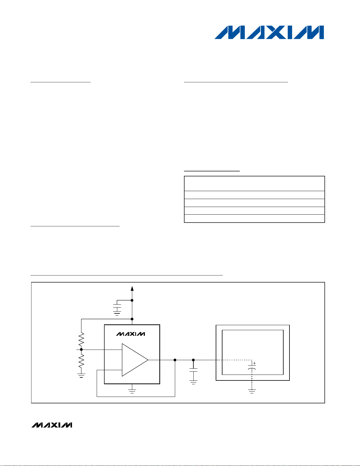
The MAX9550/MAX9551/MAX9552 provide a VCOM
source for TFT LCDs. The MAX9550/MAX9551/
MAX9552 source and sink a large current to quickly
restore the VCOM voltage, making it ideal for TFT LCDs.
The output settles to within 0.1% in less than 2µs. In
addition, the MAX9550/MAX9551/MAX9552 directly drive
the capacitive load in the VCOM layer of the TFT LCDs
without the need for a series resistor.
The MAX9550/MAX9551/MAX9552 feature single, dual,
and quad channel VCOM amplifiers, respectively. The
MAX9550/MAX9551/MAX9552 can drive up to 800mA of
peak current per channel and operate up to 20V. The
devices feature soft-start to reduce inrush current, output
short-circuit protection, and thermal shutdown.
The MAX9550 is available in a space-saving 5-pin thin
SOT23 package, and an 8-pin µMAX®package with an
exposed paddle. The MAX9551 is available in an 8-pin
µMAX package with an exposed paddle. The MAX9552
is available in a 14-pin TSSOP package. All devices are
specified over the -40°C to +85°C temperature range.
Applications
TFT-LCD Panels
Instrument Control Voltage Sources
Features
♦ Operates Up To 20V
♦ 800mA Peak Output Current
♦ Settles to Within 0.1% of V
OUT
in Less than 2µs
♦ Excellent Load Regulation
♦ Thermal-Shutdown Protection
♦ Short-Circuit Protection to Both Rails
♦ Soft-Start to Reduce Inrush Current
MAX9550/MAX9551/MAX9552
High-Current VCOM Drive Buffers
for TFT LCDs
________________________________________________________________ Maxim Integrated Products 1
Ordering Information
MAX9550
16V
SUPPLY
IN+
OUT
1µF
TFT-LCD
CAPACITANCE
V
REF
V
DD
TFT LCD
IN-
GND
Typical Operating Circuit
19-3858; Rev 2; 9/06
For pricing, delivery, and ordering information, please contact Maxim/Dallas Direct! at
1-888-629-4642, or visit Maxim’s website at www.maxim-ic.com.
Pin Configuration appears at end of data sheet.
Note: All devices specified over the -40°C to +85°C operating
temperature range.
+Denotes lead-free package.
*EP = Exposed paddle.
PART
AMPS
PIN-PACKAGE
PKG
TOP
MARK
MAX9550EZK+T
1
ADSG
MAX9550EUA+
1 8 µMAX-EP*
AABA
MAX9551EUA+
2 8 µMAX-EP*
—
MAX9552EUD+
4
—
µMAX is a registered trademark of Maxim Integrated Products, Inc.
CODE
5 Thin SOT23-5 Z5-1
U8E-2
U8E-2
14 TSSOP-EP* U14E-3
Page 2

MAX9550/MAX9551/MAX9552
High-Current VCOM Drive Buffers
for TFT LCDs
2 _______________________________________________________________________________________
ABSOLUTE MAXIMUM RATINGS
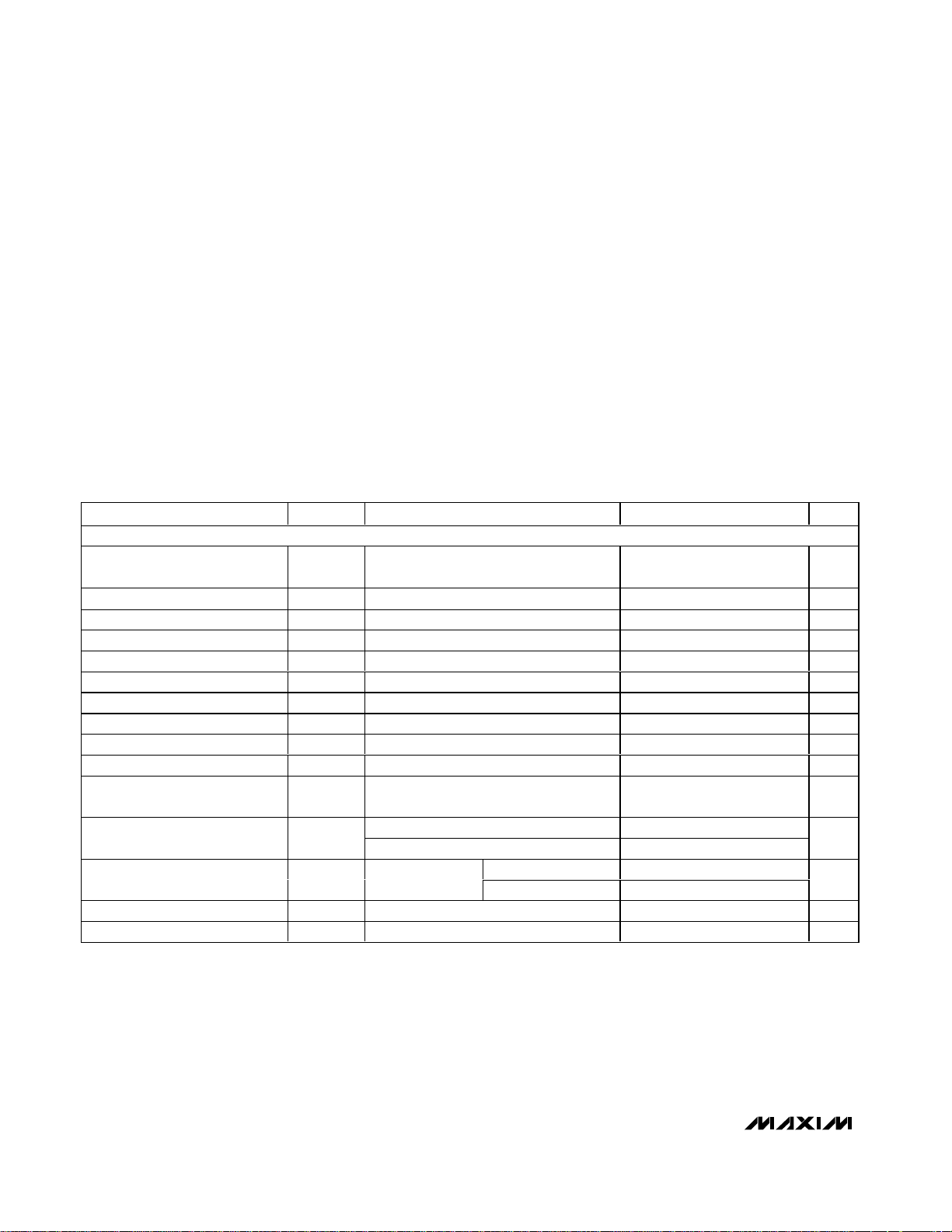
ELECTRICAL CHARACTERISTICS
(VDD= 16V, GND = 0V, V
CM
= V
OUT
= VDD/ 2, CL= 1µF, TA= T
MIN
to T
MAX
, unless otherwise noted. Typical values are at
T
A
= +25°C.) (Note 1)
Stresses beyond those listed under “Absolute Maximum Ratings” may cause permanent damage to the device. These are stress ratings only, and functional
operation of the device at these or any other conditions beyond those indicated in the operational sections of the specifications is not implied. Exposure to
absolute maximum rating conditions for extended periods may affect device reliability.
Supply Voltage (VDDto GND) ................................-0.3V to +22V
Any Other Pin to GND ................................-0.3V to (V
DD
+ 0.3V)
IN+/IN- (current) ...............................................................±20mA
OUT, OUT_ (current)................................................................1A
Continuous Power Dissipation (T
A
= +70°C)
5-Pin Thin SOT23 (derate 9.5mW/°C above +70°C)....727mW
8-Pin µMAX (derate 10.3mW/°C above +70°C) ........824.7mW
14-Pin TSSOP (derate 20.8mW/°C above +70°C) .....1667mW
Operating Temperature Range ...........................-40°C to +85°C
Junction Temperature......................................................+150°C
Storage Temperature Range .............................-65°C to +150°C
Lead Temperature (soldering, 10s) .................................+300°C
PARAMETER
CONDITIONS
TYP MAX
UNITS
DC CHARACTERISTICS
Supply Voltage Range V
DD
Inferred from PSRR test and transient
load test
720V
Quiescent Current I
CC
Per channel 2 4 mA
Low Output Voltage V
OL
IL = -4mA 0.04 0.1 V
High Output Voltage V
OH
IH = +4mA
V
Input Offset Voltage V
OS
+1 +10 mV
Input Bias Current I
B
0.01 1 µA
Input Resistance R
IN
1
MΩ
Common-Mode Input Voltage
CMVR Inferred from CMRR 2
V
Common-Mode Rejection Ratio CMRR 2V ≤ VIN ≤ (VDD - 2V) 80 96 dB
Power-Supply Rejection Ratio PSRR V
OUT
= 3.5V, VDD = 7V to 16V 80 96 dB
Continuous Output Current I
O
VDD = 7V, V
OUT
= 3.5V, guaranteed by
load, regulation test
55 mA
I
OUT
= 0mA to 50mA 6 13
Output Load Regulation LR1
I
OUT
= 0mA to -50mA 6 13
mV
6.5 15
Output Load Regulation LR2
V
DD
= 7V,
V
OUT
= 3.5V
6.5 15
mV
Thermal Shutdown +160 °C
Thermal Hysteresis 15 °C
SYMBOL
MIN
VDD - 0. 0 4 V
-10
I
= 0mA to -55mA
OUT
I
= 0mA to 55mA
OUT
- 0.1
DD
VDD - 2
Page 3

MAX9550/MAX9551/MAX9552
High-Current VCOM Drive Buffers
for TFT LCDs
_______________________________________________________________________________________ 3
Note 1: All devices are 100% production tested at TA = +25°C. All temperature limits are guaranteed by design.
ELECTRICAL CHARACTERISTICS (continued)
(VDD= 16V, GND = 0V, V
CM
= V
OUT
= VDD/ 2, CL= 1µF, TA= T
MIN
to T
MAX
, unless otherwise noted. Typical values are at
T
A
= +25°C.) (Note 1)
PARAMETER
CONDITIONS
TYP MAX
UNITS
AC CHARACTERISTICS
Settling Time t
S
Settling to 0.1% of V
OUT
, IL = 0 to 600mA,
C
L
= 1µF, RS = 2.2Ω, CS = 0.1µF
(Figure 1)
2.0 µs
Input Capacitance C
IN
1.5 pF
I
OUT
= ±50mA 13
Transconductance gm
I
OUT
= ±500mA 42
S
VDD = 7V, VIN = 1.5V
pulse for 100µs
±290
Transient Output Current
AV = 1
V
DD
= 16V, VIN = 1.5V
pulse for 100µs
±830
mA
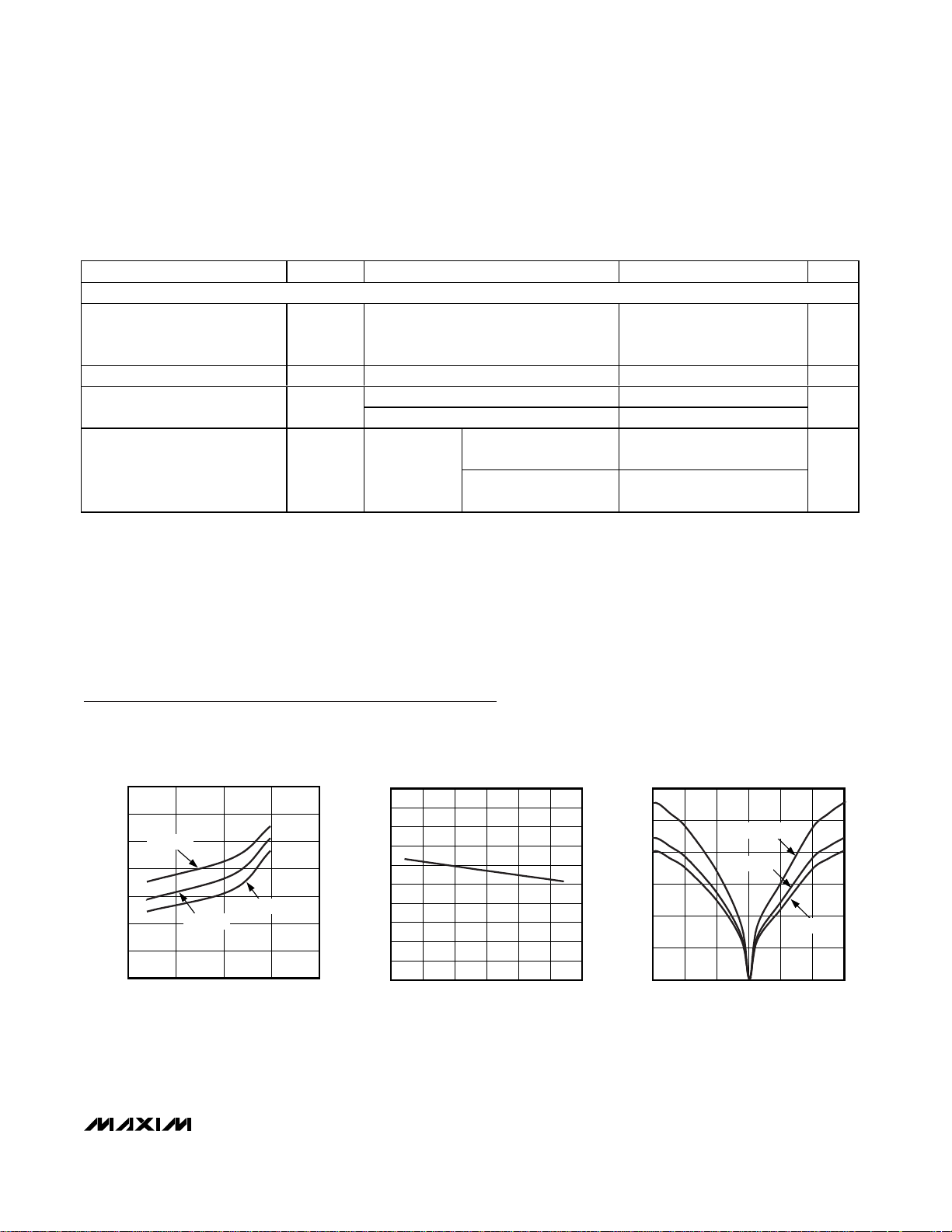
Typical Operating Characteristics
(VDD= 16V, GND = 0V, V
CM
= V
OUT
= VDD/ 2, CL= 1µF, TA = +25°C, unless otherwise noted.)
INPUT OFFSET VOLTAGE DEVIATION
vs. SUPPLY VOLTAGE
VDD (V)
V
OS
(mV)
201510
-0.1
0
0.1
0.2
0.3
0.4
0.5
-0.2
525
MAX9550 toc01
TA = -40°C
TA = +25°C
TA = +85°C
INPUT OFFSET VOLTAGE DEVIATION
vs. TEMPERATURE
MAX9550 toc02
TEMPERATURE (°C)
V
OS
(mV)
7550250-25
-0.3
-0.2
-0.1
0
0.1
0.2
0.3
0.4
0.5
0.6
-0.4
-50 100
TRANSCONDUCTANCE
vs. OUTPUT CURRENT
MAX9550 toc03
OUTPUT CURRENT (mA)
TRANSCONDUCTANCE (S)
4002000-200-400
10
20
30
40
50
60
0
-600 600
TA = -40°C
TA = +25°C
TA = +85°C
SYMBOL
I
OUTMAX
MIN
±200
±600
Page 4

MAX9550/MAX9551/MAX9552
High-Current VCOM Drive Buffers
for TFT LCDs
4 _______________________________________________________________________________________
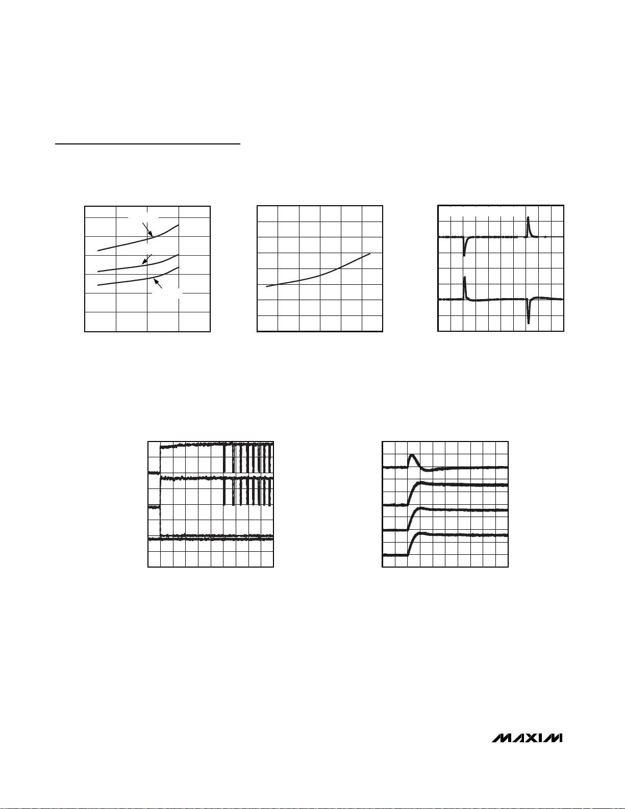
SUPPLY CURRENT
vs. SUPPLY VOLTAGE
MAX9550 toc04
SUPPLY VOLTAGE (V)
SUPPLY CURRENT (mA)
201510
0.5
1.0
1.5
2.0
2.5
3.0
0
525
TA = +85°C
TA = -40°C
TA = +25°C
SUPPLY CURRENT
vs. TEMPERATURE
MAX9550 toc05
TEMPERATURE (°C)
SUPPLY CURRENT (mA)
7550-25 0 25
0.5
1.0
1.5
2.0
2.5
3.0
3.5
4.0
0
-50 100
LOAD TRANSIENT (±600mA)
MAX9550 toc06
2µs/div
I
OUT
500mA/div
V
OUT
50mV/div
AC-COUPLED
RS = 2.2Ω, CL = 1µF, CS = 0.1µF
SHORT-CIRCUIT WAVEFORMS
MAX9550 toc07
5ms/div
V
CC
5V/div
V
OUT
5V/div
I
OUT
200mA/div
I
CC
200mA/div
STARTUP WAVEFORM
MAX9550 toc08
20µs/div
V
OUT
5V/div
IN
+
5V/div
V
CC
10V/div
I
OUT
200mA/div
Typical Operating Characteristics (continued)
(VDD= 16V, GND = 0V, V
CM
= V
OUT
= VDD/ 2, CL= 1µF, TA = +25°C, unless otherwise noted.)
Page 5

MAX9550/MAX9551/MAX9552
High-Current VCOM Drive Buffers
for TFT LCDs
_______________________________________________________________________________________ 5
Pin Description
PIN
MAX9550
THIN
SOT23
NAME FUNCTION
1 6 — — OUT VCOM Output
2 4 4 11 GND Ground
3 3 — — IN+ Positive Input
4 2 — — IN- Negative Input
57 8 4 VDDPositive Supply Input
— — 1 1 OUTA VCOM Output A
— — 3 3 INA+ Positive Input A
— — 2 2 INA- Negative Input A
—
— — N.C. No Connection. Not internally connected.
— — 5 5 INB+ Positive Input B
— — 6 6 INB- Negative Input B
— — 7 7 OUTB VCOM Output B
— — — 8 OUTC VCOM Output C
— — — 9 INC- Negative Input C
— — — 10 INC+ Positive Input C
— — — 12 IND+ Positive Input D
— — — 13 IND- Negative Input D
— — — 14 OUTD VCOM Output D
—EP EP EP EP
Exposed Paddle. EP is internally connected to GND. Connect
EP to GND.
µMAX
1, 5, 8
MAX9551 MAX9552
Page 6

MAX9550/MAX9551/MAX9552
High-Current VCOM Drive Buffers
for TFT LCDs
6 _______________________________________________________________________________________
MAX9550
16V
SUPPLY
16V
SUPPLY
*C1 = 4.7µF
C
L
= 1µF
*C2 = 0.1µF
*PLACE 4.7µF AND 0.1µF CAPACITORS AS CLOSE TO PIN AS POSSIBLE.
**R
S
INCLUDES THE GENERATOR RESISTANCE.
NOTE: PLACE C
L
AS CLOSE TO OUT PIN AS POSSIBLE AND KELVIN
SENSE THE FEEDBACK LOOP CONNECTION AS SHOWN.
0V TO 1.5V AT 50kHz
C
S
= 0.1µF**RS = 2.2Ω
IN+
OUT
V
OUT
TEST LOAD
V
REF
V
DD
IN-
GND
Figure 1. Settling Time Test Circuit
Detailed Description
The MAX9550/MAX9551/MAX9552 operational transconductance amplifiers (OTA) hold the VCOM voltage stable while providing the ability to source and sink a high
current quickly (800mA typ) into a capacitive load such
as the backplane of a TFT-LCD panel. The output settles
to within 0.1% in less than 2µs. The fast settling time is
achieved by increasing the transconductance of the
buffer as the output current increases (see the Typical
Operating Characteristics).
In addition, the MAX9550/MAX9551/MAX9552 directly
drive the capacitive load in the VCOM layer of the
TFT LCD without the need for a series resistor.
The MAX9550/MAX9551/MAX9552 unity-gain bandwidth is:
GBW = g
M
/ 2πC
OUT
where C
OUT
is the capacitive load at the output and g
M
is the transconductance.
To insure buffer stability, place a 1µF low-ESR capacitor as close to the OUT pin as possible. However, this
value may be reduced if the TFT-LCD panel load provides some of the capacitance and the resistance in
series when this capacitance is low. Connect the feedback at OUT using a Kelvin connection at the low-ESR
capacitor.
Thermal Shutdown with Temperature
Hysteresis
The MAX9550/MAX9551/MAX9552 are capable of high
output currents and therefore, feature thermal-shutdown
protection with temperature hysteresis. When the die temperature reaches +160°C, the devices shut down. When
the die cools down by 15°C, the devices turn on again.
Page 7

MAX9550/MAX9551/MAX9552
High-Current VCOM Drive Buffers
for TFT LCDs
_______________________________________________________________________________________ 7
Applications Information
Output Load Capacitor
The output load capacitor must have a low ESR value
(50mΩ or lower) and it must be placed as close as pos-
sible to the OUT pin to ensure buffer stability (see
Figure 2). Ceramic capacitors are an excellent choice.
Power Supplies and Bypass Capacitors
The MAX9550/MAX9551/MAX9552 operate from a 6V to
20V single supply, or from ±3V to ±10V dual supplies.
Proper supply bypassing ensures stability while driving
high transient loads. The MAX9550/MAX9551/MAX9552
require minimum 4.7µF (C1) and 0.1µF (C2) power-supply bypass capacitors placed as close as possible to
the power-supply pin (V
DD
). See Figure 2. For dualsupply operation, use 4.7µF and 0.1µF bypass capacitors on both supplies (V
DD
and GND) with each
capacitor placed as close as possible to the V
DD
and
GND pins.
Layout and Grounding
The exposed paddle on the µMAX and TSSOP packages provides a low thermal resistance for heat dissipation. Solder the exposed paddle to a ground plane
for best results. Do not route traces under these packages. For dual-supply operation, the exposed paddle
(EP) must be electrically connected to the negative
supply or it can be left unconnected.
MAX9550
16V
SUPPLY
*C1 = 4.7µF
C
L
= 1µF
*C2 = 0.1µF
*PLACE 4.7µF AND 0.1µF CAPACITORS AS CLOSE TO PIN AS POSSIBLE.
NOTE: PLACE C
L
AS CLOSE TO THE OUT PIN AS POSSIBLE
AND KELVIN SENSE THE FEEDBACK LOOP CONNECTION AS SHOWN.
IN+
OUT
V
OUT
TFT-LCD
CAPACITANCE
V
REF
V
DD
TFT LCD
IN-
GND
Figure 2. Typical TFT-LCD Backplane Drive Circuit
Page 8

MAX9550/MAX9551/MAX9552
High-Current VCOM Drive Buffers
for TFT LCDs
8 _______________________________________________________________________________________
GND
IN-IN+
15V
DD
OUT
MAX9550
MAX9550
THIN SOT23
TOP VIEW
2
34
1
2
3
4
8
7
6
5
N.C.
V
DD
OUT
N.C.GND
IN+
IN-
N.C.
µMAX-EP
MAX9551
MAX9552
1
2
3
4
8
7
6
5
V
DD
OUTB
INB-
INB+GND
INA+
INA-
OUTA
µMAX-EP
14
13
12
11
10
9
8
1
2
3
4
5
6
7
OUTD
IND-
IND+
GNDV
DD
INA+
INA-
OUTA
INC+
INC-
OUTCOUTB
INB-
INB+
TSSOP-EP
Pin Configurations
Chip Information
PROCESS: BiCMOS
Page 9

MAX9550/MAX9551/MAX9552
High-Current VCOM Drive Buffers
for TFT LCDs
_______________________________________________________________________________________ 9
Package Information
(The package drawing(s) in this data sheet may not reflect the most current specifications. For the latest package outline information
go to www.maxim-ic.com/packages
.)
THIN SOT23.EPS
Page 10

MAX9550/MAX9551/MAX9552
High-Current VCOM Drive Buffers
for TFT LCDs
10 ______________________________________________________________________________________
Package Information (continued)
(The package drawing(s) in this data sheet may not reflect the most current specifications. For the latest package outline information
go to www.maxim-ic.com/packages
.)
Page 11

MAX9550/MAX9551/MAX9552
High-Current VCOM Drive Buffers
for TFT LCDs
______________________________________________________________________________________ 11
8L, µMAX, EXP PAD.EPS
C
1
1
21-0107
Package Information (continued)
(The package drawing(s) in this data sheet may not reflect the most current specifications. For the latest package outline information
go to www.maxim-ic.com/packages
.)
Page 12

MAX9550/MAX9551/MAX9552
High-Current VCOM Drive Buffers
for TFT LCDs
Maxim cannot assume responsibility for use of any circuitry other than circuitry entirely embodied in a Maxim product. No circuit patent licenses are
implied. Maxim reserves the right to change the circuitry and specifications without notice at any time.
12 ____________________Maxim Integrated Products, 120 San Gabriel Drive, Sunnyvale, CA 94086 408-737-7600
© 2006 Maxim Integrated Products is a registered trademark of Maxim Integrated Products, Inc.
Package Information (continued)
(The package drawing(s) in this data sheet may not reflect the most current specifications. For the latest package outline information
go to www.maxim-ic.com/packages
.)
TSSOP 4.4mm BODY.EPS
E
1
1
21-0108
PACKAGE OUTLINE, TSSOP, 4.40 MM BODY,
EXPOSED PAD
XX XX
 Loading...