

Page 1
General Description
The MAX9532 DirectDrive®video filter amplifier is
specifically designed to work in harsh environments
such as automobiles. The MAX9532 provides integrated short-to-battery protection, allowing the output of the
device to survive shorts up to 18V.
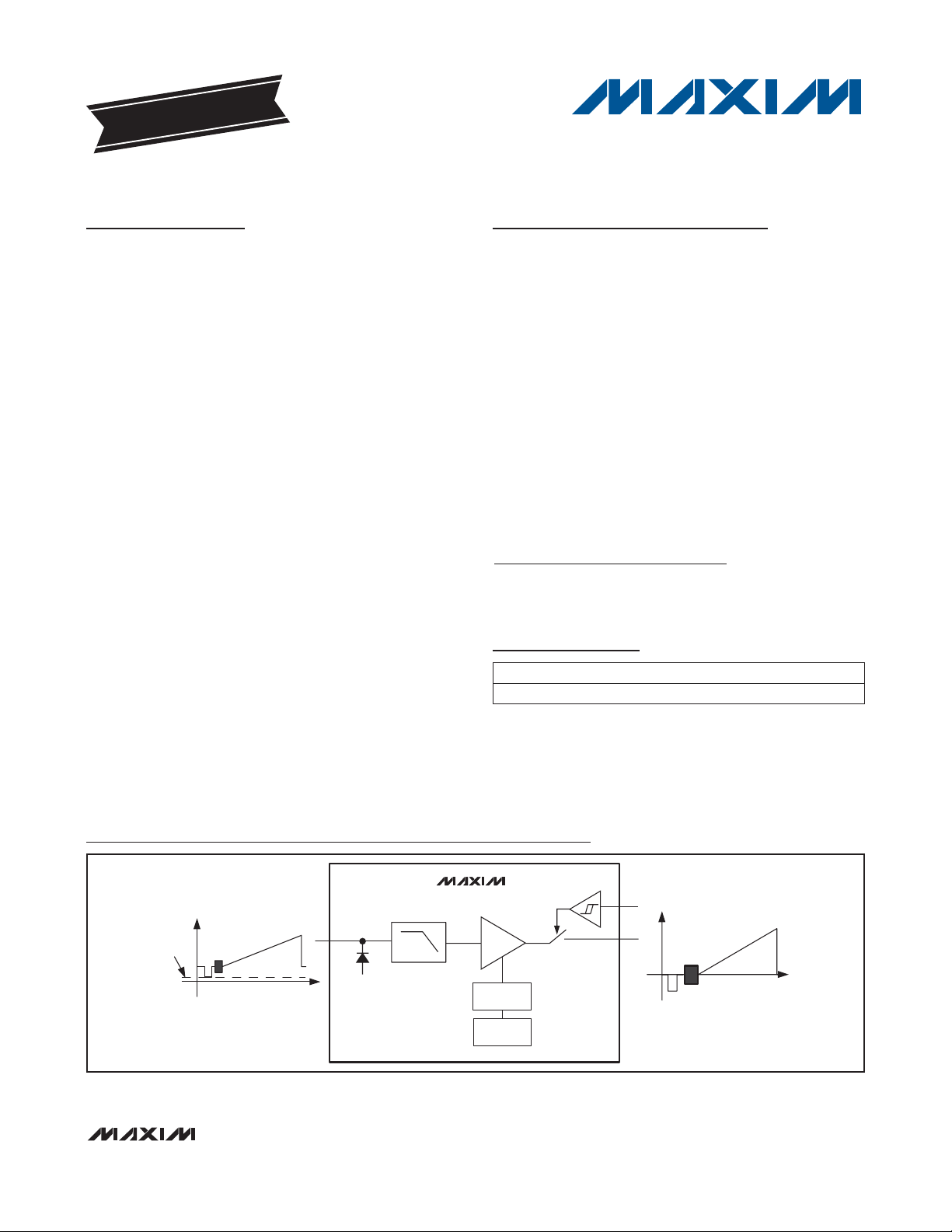
Maxim’s DirectDrive technology eliminates large output
coupling capacitors and sets the output video black
level near ground. DirectDrive requires an integrated
charge pump and an internal linear regulator to create
a clean negative power supply so that the amplifier can
pull the sync below ground. The charge pump injects
so little noise into the video output that the picture is
visibly flawless.
The MAX9532 features an internal reconstruction filter
that smoothes the steps and reduces the spikes on the
video signal from the video digital-to-analog converter
(DAC). The reconstruction filter typically provides ±1dB
passband flatness of 9.5MHz and 42dB attenuation at
27MHz.
The input of the MAX9532 can be directly connected to
the output of a video DAC. The MAX9532 also features a
transparent input sync-tip clamp, allowing AC-coupling
of input signals with different DC biases.
The MAX9532 features an internal fixed gain of 4V/V. The
input full-scale video signal is nominally 0.5V
P-P
, and the
output full-scale video signal is nominally 2V
P-P
.
The short-to-battery protection utilizes an internal switch
in series with the amplifier output. When the MAX9532
detects that the output is short circuited to the battery
voltage, the internal switch is disabled, protecting the
MAX9532 from voltages up to 18V.
The MAX9532 is available in a 3mm x 3mm, 10-pin
µMAX
®
package and is specified over the -40°C to
+125°C automotive operating temperature range.
Features
♦ Short-to-Battery Protection on Video Output (Up
to 18V)
♦ DirectDrive Sets Video Output Black Level Near
Ground
♦ DirectDrive Eliminates DC-Blocking Capacitors at
the Output
♦ 3.3V Single-Supply Operation
♦ Reconstruction Filter with 9.5MHz Passband and
42dB Attenuation at 27MHz
♦ DC-Coupled Input/Output
♦ Transparent Input Sync-Tip Clamp
♦ 4V/V Internal Fixed Gain
MAX9532
DirectDrive Video Amplifier with
Short-to-Battery Protection
________________________________________________________________
Maxim Integrated Products
1
19-4431; Rev 0; 2/09
For pricing, delivery, and ordering information, please contact Maxim Direct at 1-888-629-4642,
or visit Maxim’s website at www.maxim-ic.com.
EVALUATION KIT
AVAILABLE
Ordering Information
+
Denotes a lead(Pb)-free/RoHS-compliant package.
DirectDrive is a registered trademark of Maxim Integrated Products, Inc.
µMAX is a registered trademark of Maxim Integrated Prodcuts, Inc.
Simplified Block Diagram
Applications
Automotive Infotainment Systems
Pin Configuration and Functional Diagram/Typical
Application Circuits appear at end of data sheet.
PART PIN-PACKAGE TEMP RANGE
MAX9532AUB+ 10 µMAX -40°C to +125°C
MAX9532
500mV
VIDEO
P-P
IN
TRANSPARENT
CLAMP
LPF
LINEAR
REGULATOR
CHARGE
PUMP
AV = 4V/V
JACKSENSE
OUT
0V
2V
VIDEO
P-P
Page 2
MAX9532
DirectDrive Video Amplifier with
Short-to-Battery Protection
2 _______________________________________________________________________________________
ABSOLUTE MAXIMUM RATINGS
ELECTRICAL CHARACTERISTICS
(VDD= 3.3V, GND = CPGND = 0, RL= 100Ω to GND, C1= C2= C3= 1µF, TA= T
MIN
to T
MAX
, unless otherwise noted. Typical val-
ues are at T
A
= +25°C.) (Note 1)
Stresses beyond those listed under “Absolute Maximum Ratings” may cause permanent damage to the device. These are stress ratings only, and functional
operation of the device at these or any other conditions beyond those indicated in the operational sections of the specifications is not implied. Exposure to
absolute maximum rating conditions for extended periods may affect device reliability.
VDDto GND..............................................................-0.3V to +4V
V
DD
to CPGND .........................................................-0.3V to +4V
CPGND to GND.....................................................-0.1V to +0.1V
IN to GND .................................................................-0.3V to +4V
JACKSENSE to GND........................................The higher of V
SS
and -2V to (VSS+ 22V)
OUT to GND ............The higher of V
SS
and -1.5V to (VSS+ 22V)
V
SS
to CPVSS ........................................................-0.1V to +0.1V
Continuous Current
IN, JACKSENSE............................................................±20mA
C1P, C1N, CPVSS ........................................................±50mA
OUT ..............................................................................±50mA
Continuous Power Dissipation (T
A
= +70°C)
10-Pin µMAX (derate 8.8mW/°C above +70°C) ........707.3mW
Operating Temperature Range .........................-40°C to +125°C
Junction Temperature......................................................+150°C
Storage Temperature Range .............................-65°C to +150°C
Lead Temperature (soldering, 10s) .................................+300°C
DC-COUPLED INPUT
Input Voltage Range V
Input Current I
Input Resistance R
SYNC-TIP CLAMP INPUT
Sync-Tip Clamp Level V
Input Voltage Range
Sync Crush
Input Clamping Current Sync-tip clamp 2 3.3 µA
Max Input Source Resistance 300 Ω
GENERAL
Supply Voltage Range V
Quiescent Supply Current 15 23 mA
DC Voltage Gain A
Output Level VIN = 150mV -0.120 +0.150 V
PARAMETER SYMBOL CONDITIONS MIN TYP MAX UNITS
Guaranteed by output voltage swing
IN
IN
IN
CLP
DD
V
3V < V
Guaranteed by output voltage swing
3.135V < V
VIN = 0.5V 2 3.3 µA
0.1V ≤ VIN ≤ 0.5V 5 MΩ
Sync-tip clamp -6.2 -1.63 +3.5 mV
Guaranteed by output voltage swing
3V < V
Guaranteed by output voltage swing
V
DD
Sync-tip clamp; percentage reduction in
sync pulse (0.15V
impedance), guaranteed by input clamping
current measurement
Guaranteed by PSRR 3.0 3.3 3.6 V
Guaranteed by output voltage swing 3.92 4 4.08 V/V
< 3.135V
DD
DD
< 3.135V
DD
> 3.135V
< 3.6V
P-P
, 75Ω source
0 0.5
0 0.7
0 0.5
0 0.7
2.3 %
V
V
P-P
Page 3
MAX9532
DirectDrive Video Amplifier with
Short-to-Battery Protection
_______________________________________________________________________________________ 3
ELECTRICAL CHARACTERISTICS (continued)
(VDD= 3.3V, GND = CPGND = 0, RL= 100Ω to GND, C1= C2= C3= 1µF, TA= T
MIN
to T
MAX
, unless otherwise noted. Typical val-
ues are at T
A
= +25°C.) (Note 1)
Output Voltage Swing
Output Short-Circuit Current 90 mA
Output Resistance R
Short Circuit to Battery Current Short-to-battery, V
Power-Supply Rejection Ratio 3.0V ≤ VDD ≤ 3.6V 46 78 dB
Filter
Differential Gain DG
Differential Phase DP
2T Pulse-to-Bar K Rating
2T Pulse Response 2T = 200ns, RL = 100Ω to -2V and +2V 0.4 K%
2T Bar Response
Nonlinearity 5-step staircase; RL = 100Ω to -2V and +2V 0.1 %
Group Delay Distortion
Glitch Impulse Caused by
Charge Pump Switching
Peak Signal to RMS Noise
Power-Supply Rejection Ratio
Output Impedance f = 5MHz 2 Ω
JACKSENSE Input Resistance 120 250 kΩ
BATTERY DETECTION
Threshold Accuracy Referred to GND 7.3 8 8.7 V
Video Output Disconnect Time After detection of short-to-battery 20 µs
Video Output Connect Time After short-to-battery has been removed 4.9 10 20 ms
PARAMETER SYMBOL CONDITIONS MIN TYP MAX UNITS
Measured at output, VDD = 3.135V,
V
= V
OUT
IN
-2V and +2V
Measured at output, V
to (V
V
IN
frequency is 100kHz
5-step modulated staircase, f = 4.43MHz,
= 100Ω to -2V and +2V
R
L
5-step modulated staircase, f = 4.43MHz,
= 100Ω to -2V and +2V
R
L
2T = 200ns; bar time is 18µs; the beginning
2.5% and the ending 2.5% of the bar time is
ignored; R
2T = 200ns; bar time is 18µs; the beginning
2.5% and the ending 2.5% of the bar time is
ignored; R
100kHz ≤ f ≤ 5MHz, outputs are 2V
= 100Ω to -2V and +2V
R
L
Measured at outputs, RL = 100Ω to -2V and
+2V
100kHz ≤ f ≤ 5MHz, R
+2V
f = 100KHz, 100mV
and +2V
to (V
CLP
+ 0.5V), RL = 100Ω to -2V and +2V
CLP
= 0.5V
P-P
= 100Ω to -2V and +2V
L
= 100Ω to -2V and +2V
L
+ 0.7V), RL = 100Ω to
CLP
= 3V, VIN = V
DD
= 9V to 16V 3 mA
OUT
, reference
= 100Ω to -2V and
L
; RL = 100Ω to -2V
P-P
Attenuation at
5.5MHz
Attenuation at
f = 27MHz
P-P
2.744 2.8 2.856
CLP
;
1.96 2 2.04
0.1 Ω
-1.29 +1
20 42
0.7 %
0.5 deg
0.5 K%
0.1 K%
13 ns
40 pVs
64 dB
47 dB
V
P-P
dB
Page 4
MAX9532
DirectDrive Video Amplifier with
Short-to-Battery Protection
4 _______________________________________________________________________________________
ELECTRICAL CHARACTERISTICS (continued)
(VDD= 3.3V, GND = CPGND = 0, RL= 100Ω to GND, C1= C2= C3= 1µF, TA= T
MIN
to T
MAX
, unless otherwise noted. Typical val-
ues are at T
A
= +25°C.) (Note 1)
Note 1: All devices are 100% production tested at TA= +25°C. Specifications over temperature limits are guaranteed by design.
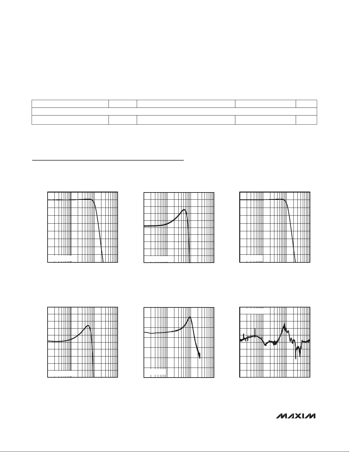
SMALL-SIGNAL GAIN vs. FREQUENCY
MAX9532 toc01
FREQUENCY (MHz)
GAIN (dB)
101
-35
-30
-25
-20
-15
-10
-5
0
5
-40
0.1 100
VIN = 0.025V
P-P
NOTE: GAIN VALUES (PLOTTED IN dB) ARE NORMALIZED
VALUES RELATIVE TO THE EXPECTED VALUE OF 4V/V.
SMALL-SIGNAL GAIN FLATNESS
vs. FREQUENCY
MAX9532 toc02
FREQUENCY (MHz)
GAIN (dB)
101
-0.8
-0.6
-0.4
-0.2
0
0.2
0.4
0.6
0.8
1.0
-1.0
0.1 100
VIN = 0.025V
P-P
NOTE: GAIN VALUES (PLOTTED IN dB) ARE NORMALIZED
VALUES RELATIVE TO THE EXPECTED VALUE OF 4V/V.
LARGE-SIGNAL GAIN vs. FREQUENCY
MAX9532 toc03
FREQUENCY (MHz)
GAIN (dB)
101
-35
-30
-25
-20
-15
-10
-5
0
5
-40
0.1 100
VIN = 0.5V
P-P
NOTE: GAIN VALUES (PLOTTED IN dB) ARE NORMALIZED
VALUES RELATIVE TO THE EXPECTED VALUE OF 4V/V.
LARGE-SIGNAL GAIN FLATNESS
vs. FREQUENCY
MAX9532 toc04
FREQUENCY (MHz)
GAIN (dB)
101
-0.8
-0.6
-0.4
-0.2
0
0.2
0.4
0.6
0.8
1.0
-1.0
0.1 100
VIN = 0.5V
P-P
NOTE: GAIN VALUES (PLOTTED IN dB) ARE NORMALIZED
VALUES RELATIVE TO THE EXPECTED VALUE OF 4V/V.
GROUP DELAY vs. FREQUENCY
MAX9532 toc05
FREQUENCY (MHz)
GROUP DELAY (ns)
101
-20
0
20
40
60
80
100
-40
0.1 100
VIN = 0.5V
P-P
POWER-SUPPLY REJECTION RATIO
vs. FREQUENCY
MAX9532 toc06
FREQUENCY (MHz)
PSRR (dB)
101
-90
-80
-70
-60
-50
-40
-30
-20
-10
0
-100
0.1 100
V
RIPPLE
= 100mV
P-P
Typical Operating Characteristics
(VDD= 3.3V, GND = CPGND = 0, video output has RL= 100Ω to GND, C1= C2= C3= 1μF, TA= +25°C, unless otherwise noted.)
PARAMETER SYMBOL CONDITIONS MIN TYP MAX UNITS
CHARGE PUMP
Switching Frequency f
CP
220 440 660 kHz
Page 5

MAX9532
DirectDrive Video Amplifier with
Short-to-Battery Protection
_______________________________________________________________________________________ 5
Typical Operating Characteristics (continued)
(VDD= 3.3V, GND = CPGND = 0, video output has RL= 100Ω to GND, C1= C2= C3= 1μF, TA= +25°C, unless otherwise noted.)
QUIESCENT CURRENT vs. TEMPERATURE
14.70
VSS = 3.3V
14.69
14.68
14.67
14.66
14.65
14.64
14.63
SUPPLY CURRENT (mA)
14.62
14.61
14.60
14.59
-40
= 0V
V
IN
NO LOAD
TEMPERATURE (°C)
OUTPUT VOLTAGE vs. INPUT VOLTAGE
AV = 4.012V/V
3
2
1
0
OUTPUT VOLTAGE (V)
-1
-2
-0.2 1.0
INPUT VOLTAGE (V)
4.020
4.018
MAX9532 toc07
1106010
MAX9532 toc09
0.80.60.40.20
4.016
4.014
4.012
4.010
GAIN (V/V)
4.008
4.006
4.004
4.002
4.000
-0.5
-1.0
DIFFERENTIAL GAIN (%)
-0.5
-1.0
DIFFERENTIAL PHASE (deg)
DC GAIN vs. TEMPERATURE
-40
TEMPERATURE (°C)
DIFFERENTIAL GAIN AND PHASE
1.0
0.5
0
f = 3.58MHz
= +25°C
T
A
1324567
DIFFERENTIAL PHASE
1.0
0.5
0
f = 3.58MHz
= +25°C
T
A
1324567
MAX9532 toc08
1106010
MAX9532 toc10
DIFFERENTIAL GAIN AND PHASE
1.0
f = 4.43MHz
0.5
= +25°C
T
A
0
-0.5
-1.0
DIFFERENTIAL GAIN (%)
1324567
MAX9532 toc11
2T RESPONSE
MAX9532 toc12
V
IN
100mV/div
DIFFERENTIAL PHASE
1.0
0.5
0
-0.5
-1.0
1324567
DIFFERENTIAL PHASE (deg)
f = 4.43MHz
= +25°C
T
A
100ns/div
V
OUT
400mV/div
Page 6

MAX9532
DirectDrive Video Amplifier with
Short-to-Battery Protection
6 _______________________________________________________________________________________
Typical Operating Characteristics (continued)
(VDD= 3.3V, GND = CPGND = 0, video output has RL= 100Ω to GND, C1= C2= C3= 1μF, TA= +25°C, unless otherwise noted.)
100μs/div
OUTPUT SHORT-TO-BATTERY
RESPONSE
V
JACKSENSE
10V/div
V
OUT
500mV/div
MAX9532 toc16
0V
0V
2ms/div
OUTPUT SHORT-TO-BATTERY
RESPONSE
V
JACKSENSE
10V/div
V
OUT
500mV/div
MAX9532 toc17
0V
0V
400ns/div
2T RESPONSE
V
IN
100mV/div
V
OUT
400mV/div
MAX9532 toc13
10μs/div
VIDEO TEST SIGNAL
V
IN
200mV/div
V
OUT
800mV/div
MAX9532 toc14
2ms/div
FIELD SQUARE-WAVE RESPONSE
V
IN
200mV/div
V
OUT
800mV/div
MAX9532 toc15
Page 7

Detailed Description
The MAX9532 DirectDrive video amplifier with short-tobattery protection features an internal 5-pole
Butterworth lowpass filter with the amplifier configured
with a gain of 4. The MAX9532 accepts DC-coupled or
AC-coupled full-scale input signals of 0.5V
P-P
.
Integrated short-to-battery protection prevents the
MAX9532 from being damaged when the output is
short circuited to the battery in automotive applications.
DirectDrive
Background
Integrated video filter amplifier circuits operate from a
single supply. The positive power supply usually creates video output signals that are level-shifted above
ground to keep the signal within the linear range of the
output amplifier. For applications where the positive DC
level is not acceptable, a series capacitor can be
inserted in the output connection to eliminate the positive DC level shift. The series capacitor cannot truly
level shift a video signal because the average level of
the video varies with picture content. The series capacitor biases the video output signal around ground, but
the actual level of the video signal can vary significantly
depending upon the RC time constant and the picture
content.
The series capacitor creates a highpass filter. Since the
lowest frequency in video is the frame rate, which is
between 24Hz and 30Hz, the pole of the highpass filter is
ideally an order of magnitude lower in frequency than
the frame rate. Therefore, the series capacitor must
be very large, typically from 220µF to 3000µF. For
space-constrained equipment, the series capacitor is
unacceptable. Changing from a single series capacitor to
a SAG network that requires two smaller capacitors can
only reduce space and cost slightly.
Video Amplifier
When the full-scale video signal from a video DAC is
500mV, the black level of the video signal created by
the video DAC is around 150mV. The MAX9532 shifts
the black level to near ground at the output so that the
active video is above ground and the sync is below
ground. The amplifier needs a negative supply for the
output stage to remain in the linear region when driving
sync below ground.
The MAX9532 includes an integrated charge pump and
linear regulator to create a low-noise negative supply
from the positive supply voltage. The charge pump
inverts the positive supply to create a raw negative voltage that is then fed into the linear regulator filtering out
the charge-pump noise.
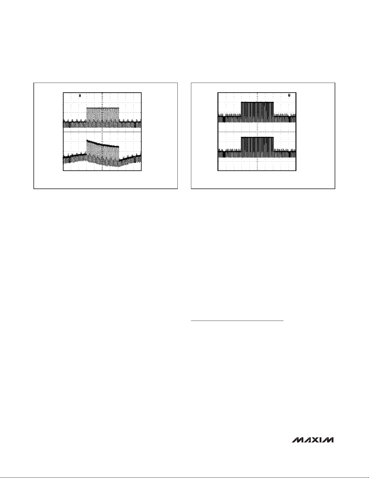
Comparison Between DirectDrive Output
and AC-Coupled Output
The actual level of the video signal varies less with a
DirectDrive output than with an AC-coupled output. The
average video signal level changes depending upon
the picture content. With an AC-coupled output, the
average level changes according to the time constant
formed by the series capacitor and series resistance
(usually 150Ω). For example, Figure 1 shows an ACcoupled video signal alternating between a completely
black screen and a completely white screen. Notice the
excursion of the video signal as the screen changes.
MAX9532
DirectDrive Video Amplifier with
Short-to-Battery Protection
_______________________________________________________________________________________ 7
Pin Description
PIN NAME FUNCTION
1VDDPositive Power Supply. Bypass VDD with a 1µF capacitor to GND.
2 C1P Charge-Pump Flying Capacitor Positive Terminal. Connect a 1µF ceramic capacitor from C1P to C1N.
3 CPGND Charge-Pump Ground. Connect to GND.
4 C1N
5 CPVSS
6VSSNegative Power Supply. Connect VSS to CPVSS.
7 OUT Video Output
8 JACKSENSE Jack-Sense Input. Connect to the video output connector after the back-termination resistor.
9 GND Ground
10 IN Video Input
Charge-Pump Flying Capacitor Negative Terminal. Connect a 1µF ceramic capacitor from C1P to
C1N.
Charge-Pump Negative Power Supply. Bypass CPVSS
10nF low ESL capacitor to GND.
with a 1µF ceramic capacitor in parallel with a
Page 8
MAX9532
With the DirectDrive amplifier, the black level is held at
ground. The video signal is constrained between
-0.3V to +0.7V. Figure 2 shows the video signal from a
DirectDrive amplifier with the same input signal as the
AC-coupled system.
Video Reconstruction Filter
The MAX9532 features an internal five-pole, Butterworth
lowpass filter to condition the video signal. The reconstruction filter smoothes the steps and reduces the
spikes created whenever the DAC output changes
value. In the frequency domain, the steps and spikes
cause images of the video signal to appear at multiples
of the sampling clock frequency. The reconstruction filter typically provides ±1dB passband flatness of
9.5MHz and 42dB attenuation at 27MHz.
Transparent Sync-Tip Clamp
The MAX9532 contains an integrated, transparent synctip clamp. When using a DC-coupled input, the sync-tip
clamp does not affect the input signal as long as the
input signal remains above ground. When using an ACcoupled input, the sync-tip clamp automatically clamps
the input signal to ground, preventing the input signal
from going lower. A low current of 2µA pulls down on
the input to prevent an AC-coupled signal from drifting
outside the input range of the device.
Short-Circuit
and Short-to-Battery Protection
The MAX9532 typical operating circuit includes a 50Ω
or 75Ω back-termination resistor that limits short-circuit
current when an external short is applied to the video
output. The MAX9532 also features an internal output
short-circuit protection to prevent device damage in
prototyping and applications where the amplifier output
can be directly shorted to ground.
To protect the device from output short circuits to voltages higher than the supply voltage V
DD
, the MAX9532
utilizes an internal switch in series with the amplifier output. When the JACKSENSE input detects that the output connector of the circuit is shorted to the battery
voltage (up to 18V) higher than the internal 8V threshold, an internal comparator disables the switch in 10µs
(typ) preventing the MAX9532 from being damaged.
After the output is shorted to a battery, the output
immediately resumes normal operation when the short
is removed within 1ms. When the output is shorted to
the battery for longer than 1ms, the output resumes normal operation 10ms after the short is removed.
Applications
Power Consumption
Quiescent power consumption is defined when the
MAX9532 is operating without load. In this case, the
MAX9532 consumes about 47.355mW. Average power
consumption, when the MAX9532 drives a 100Ω and
150Ω load to ground with a 50% flat field, is about
51.596mW and 49.513mW, respectively. Table 1 shows
the power consumption with different video signals.
Notice that the two extremes in power consumption
occur with a video signal that is all black and a video
signal that is all white. The power consumption with
75% color bars and 50% flat field lies in between the
extremes.
DirectDrive Video Amplifier with
Short-to-Battery Protection
8 _______________________________________________________________________________________
Figure 1. AC-Coupled Output
Figure 2. DirectDrive Output
INPUT
500mV/div
OUTPUT
500mV/div
2ms/div
INPUT
0V
0V
2ms/div
500mV/div
OUTPUT
1V/div
Page 9

Interfacing to Video DACs that Produce
Video Signals Higher than 0.5V
P-P
Devices designed to generate 1V
P-P
video signals at
the output of the video DAC can work with the
MAX9532. Most video DACs source current into a
ground-referenced resistor, which converts the current
into a voltage. Figure 3 shows a video DAC that creates
a video signal from 0V to 1V across a 150Ω resistor.
With a gain of 2V/V, the following video filter produces a
2V
P-P
output.
The MAX9532 accepts input signals that are 0.5V
P-P
nominally. The video DAC in Figure 3 can be made to
work with the MAX9532 by scaling down the 150Ω
resistor to a 75Ω resistor, as shown in Figure 4. The
75Ω resistor is one-half the size of the 150Ω resistor,
resulting in a video signal that is one-half the amplitude.
Video Source with a Positive DC Bias
In some applications, the video source generates a signal with a positive DC voltage bias, i.e., the sync tip of
the signal is well above ground. Figure 5 shows an
example in which the outputs of the luma (Y) DAC and
the chroma (C) DAC are connected together. Since the
DACs are current-mode, the output currents sum
together into the resistor, which converts the resulting
current into a voltage representing a composite video
signal.
When the chroma DAC is connected to an independent
output resistor to ground, the chroma signal, which is a
carrier at 3.58MHz for NTSC or at 4.43MHz for PAL,
generates a positive DC bias to keep the signal above
ground at all times. When the luma DAC is connected
to an independent output resistor to ground, the luma
signal usually does not have a positive DC bias, and
the sync tip is at approximately ground. When the chroma and luma signals are added together, the resulting
composite video signal generates a positive DC bias.
Therefore, the signal must be AC-coupled into the
MAX9532 because the composite video signal is above
the nominal 0V to 0.7V DC-coupled input range.
Video Signal Routing
Minimize the length of the PCB trace between the output of the video DAC and the input of the MAX9532 to
reduce coupling of external noise into the video signal.
If possible, shield the PCB trace.
MAX9532
DirectDrive Video Amplifier with
Short-to-Battery Protection
_______________________________________________________________________________________ 9
Figure 3. Typically, a Video DAC Generates a 1V
P-P
Signal
Across a 150
Ω
Resistor Connected to Ground
Figure 4. Video DAC Generates a 0.5V
P-P
Signal Across a 75
Ω
Resistor Connected to Ground
Table 1. Power Consumption of the MAX9532 with Different Video Signals
Note: The supply voltage is 3.3V.
IMAGE
PROCESSOR
ASIC
0V TO 1V
DAC
GENERIC 2V/V CONFIGURATION
150Ω
LPF
2V/V
2V
P-P
IMAGE
PROCESSOR
ASIC
0V TO 0.5V
DAC
75Ω
MAX9532
LPF
VIDEO SIGNAL
All Black Screen 51.236 53.978
All White Screen 57.077 65.399
75% Color Bars 53.074 57.486
50% Flat Field 49.513 51.596
MAX9532 POWER CONSUMPTION (mW)
WITH 150Ω LOAD
MAX9532 POWER CONSUMPTION (mW)
WITH 100Ω LOAD
4V/V
2V
P-P
Page 10

Power-Supply Bypassing
and Ground Management
The MAX9532 operates from a 3V to 3.6V single supply
and requires proper layout and bypassing. For the best
performance, place the components as close as possible to the device.
Proper grounding improves performance and prevents
any switching noise from coupling into the video signal.
Bypass the analog supply (V
DD
) with a 1µF capacitor to
GND, placed as close as possible to the device.
Bypass CPVSS to GND with a 1µF ceramic capacitor in
parallel with a 10nF low-ESR capacitor. The bypass
capacitors should be placed as close as possible to
the device.
MAX9532
DirectDrive Video Amplifier with
Short-to-Battery Protection
10 ______________________________________________________________________________________
Figure 5. Luma (Y) and Chroma (C) Signals are Added Together to Create a Composite Video Signal, Which is AC-Coupled into the
MAX9532
LINEAR
REGULATOR
CPVSS
C2
1μF || 10nF
MAX9532
V
SS
JACKSENSE
OUT
50Ω
50Ω
VIDEO
ASIC
DAC
DAC
V
DD
A
= 4V/V
Y
IN
0.1μF
C
1μF
3.3V
C3
V
DD
CLAMP
GND CPGND
LPF
V
AMP
DC
LEVEL SHIFT
CHARGE PUMP
C1P C1N
Page 11

MAX9532
DirectDrive Video Amplifier with
Short-to-Battery Protection
______________________________________________________________________________________ 11
Functional Diagram/Typical Application Circuits
(DC-Coupled Input/Inactive Input Clamp)
Chip Information
PROCESS: BiCMOS
1
2
3
4
5
10
9
8
7
6
IN
GND
JACKSENSE
OUTC1N
CPGND
C1P
V
DD
MAX9532
μMAX
TOP VIEW
V
SS
CPVSS
+
Pin Configuration
LINEAR
REGULATOR
CPVSS
C2
1μF || 10nF
MAX9532
V
SS
VIDEO
ASIC
DAC
1μF
V
DD
A
= 4V/V
V
IN
3.3V
C3
V
DD
TRANSPARENT
CLAMP
GND CPGND
LPF
LEVEL SHIFT
C1P C1N
AMP
DC
CHARGE PUMP
C1
1μF
JACKSENSE
OUT
50Ω
50Ω
Page 12

MAX9532
DirectDrive Video Amplifier with
Short-to-Battery Protection
Maxim cannot assume responsibility for use of any circuitry other than circuitry entirely embodied in a Maxim product. No circuit patent licenses are
implied. Maxim reserves the right to change the circuitry and specifications without notice at any time.
12
____________________Maxim Integrated Products, 120 San Gabriel Drive, Sunnyvale, CA 94086 408-737-7600
© 2009 Maxim Integrated Products Maxim is a registered trademark of Maxim Integrated Products, Inc.
PACKAGE TYPE PACKAGE CODE DOCUMENT NO.
10 µMAX U10+2
21-0061
Package Information
For the latest package outline information and land patterns, go to www.maxim-ic.com/packages.
10LUMAX.EPS
α
α
 Loading...