

Page 1
General Description
Packaged in a 1mm x 1mm UCSP™ with 4 bumps, the
MAX9519 is an ultra-small standard-definition video filter amplifier with automatic shutdown.
The automatic shutdown circuitry eliminates the need
for a shutdown control. This feature provides intelligent
power management by disabling the filter and output
amplifier in the absence of a video input signal and/or
an output video load. At shutdown, the device consumes only 1.8µA.
The MAX9519 features an internal reconstruction filter
that smooths the steps and reduces the spikes on the
video signal from the video digital-to-analog converter
(DAC). The reconstruction filter typically has ±1dB
passband flatness to 9MHz and typically 48.5dB of
attenuation at 27MHz.
The video input to the MAX9519 can be directly connected to the DAC output. The MAX9519 has an internal fixed gain of 4V/V and expects a nominal full-scale
video input signal of 0.5V
P-P
. The MAX9519 is specified
to operate over the -40°C to +125°C automotive temperature range.
Applications
Mobile Phones
Digital Still Cameras (DSC)
Digital Video Camcorders (DVC)
Portable or Space-Constrained Applications
Features
o Ultra-Small, 4-Bump, 1mm x 1mm UCSP
o Automatic Shutdown
o DC-Coupled Input and Output
o 2.7V to 3.6V Single-Supply Operation
o Reconstruction Filter with 9MHz Passband and
48.5dB Attenuation at 27MHz
o 1.8µA Shutdown Supply Current
MAX9519
1mm x 1mm Video Filter Amplifier with
Automatic Shutdown and 4V/V Gain
________________________________________________________________
Maxim Integrated Products
1
Ordering Information
AV = 4V/V
OUTIN
BUFFER
LPF
AUTOMATIC
SHUTDOWN
CONTROL LOGIC
MAX9519
0mV
TO
25mV
300mV
TO
400mV
0.5V
P-P
VIDEO
2V
P-P
VIDEO
Block Diagram
OUT
V
DD
IN
GND
12
A
B
MAX9519
UCSP
(1mm × 1mm)
TOP VIEW
(BUMPS FACING DOWN)
Pin Configuration
19-4231; Rev 0; 8/08
For pricing, delivery, and ordering information, please contact Maxim Direct at 1-888-629-4642,
or visit Maxim’s website at www.maxim-ic.com.
PART PIN-PACKAGE
TOP MARK
MAX9519ARS+T 4 UCSP AAA
Note: This device is specified over the -40°C to +125°C operating temperature range.
+
Denotes a lead-free/RoHS-compliant package.
T = Tape and reel.
UCSP is a trademark of Maxim Integrated Products, Inc.
Page 2
MAX9519
1mm x 1mm Video Filter Amplifier with
Automatic Shutdown and 4V/V Gain
2 _______________________________________________________________________________________
ABSOLUTE MAXIMUM RATINGS
ELECTRICAL CHARACTERISTICS
(VDD= 3.3V, video output has RL= 150Ω connected to GND, TA = T
MIN
to T
MAX
, unless otherwise noted. Typical values are at
T
A
= +25°C.) (Note 1)
Stresses beyond those listed under “Absolute Maximum Ratings” may cause permanent damage to the device. These are stress ratings only, and functional
operation of the device at these or any other conditions beyond those indicated in the operational sections of the specifications is not implied. Exposure to
absolute maximum rating conditions for extended periods may affect device reliability.
(Voltages with respect to GND.)
V
DD
.................................................................................0 to +4V
IN ............................................................................. -0.3V to +4V
OUT (during shutdown)............................. -0.3V to +V
DD
+ 0.3V
Continuous Current
IN ...................................................................................±20mA
Continuous Power Dissipation (T
A
= +70°C)
4-Bump UCSP (derate 3mW/°C above +70°C).............239mW
Maximum Output Current
OUT ................................................................................±100mA
Operating Temperature Range .........................-40°C to +125°C
Junction Temperature......................................................+150°C
Storage Temperature Range .............................-65°C to +150°C
Bump Temperature (soldering)
Infrared (15s) ................................................................+220°C
Vapor Phase (60s) ........................................................+215°C
PARAMETER SYMBOL CONDITIONS MIN TYP MAX UNITS
Supply Voltage Range V
Supply Current I
AUTOMATIC SHUTDOWN
Minimum Line Frequency 7.3 kHz
Sync Slice Level 1.7 3.0 %V
Output Load Detect Threshold 200 Ω
DC CHARACTERISTICS
Input Voltage Range
Input Current I
Input Resistance R
DC Voltage Gain A
Output Level IN = GND 0.18 0.325 0.475 V
Output-Voltage Swing Measured at output
DD
DD
Guaranteed by PSRR test 2.7 3.6 V
Automatic shutdown
mode
Active-detect mode
RL = 150Ω connected to GND, IN has a
black-burst video signal with a sync tip,
quiescent current only; no load current is
included
Guaranteed by
output-voltage swing
IN = GND 1 5 µA
B
IN
G uar anteed b y outp ut- vol tag e sw i ng ( N ote 2) 3.92 4 4.08 V/V
V
No load, IN does not
have an active video
signal
No load, IN has a
black-burst video
signal with a sync tip
at GND
2.7V ≤ VDD ≤ 3.6V 0 0.525
3.0V ≤ V
VDD = 2.7V,
0 ≤ V
V
DD
0 ≤ V
1.8 4
5.4
2.9 4.8 mA
≤ 3.6V 0 0.6
DD
20 MΩ
≤ 0.525V
IN
= 3.0V,
≤ 0.6V
IN
2.058 2.1 2.145
2.352 2.4 2.450
µA
DD
V
V
P-P
Page 3
MAX9519
1mm x 1mm Video Filter Amplifier with
Automatic Shutdown and 4V/V Gain
_______________________________________________________________________________________ 3
Note 1: All devices are 100% production tested at TA= +25°C. Specifications over temperature limits are guaranteed by design.
Note 2: Voltage gain (A
V
) is a two-point measurement in which the output-voltage swing is divided by the input-voltage swing.
ELECTRICAL CHARACTERISTICS (continued)
(VDD= 3.3V, video output has RL= 150Ω connected to GND, TA = T
MIN
to T
MAX
, unless otherwise noted. Typical values are at
T
A
= +25°C.) (Note 1)
Output Resistance R
Output Leakage Current
Power-Supply Rejection Ratio PSRR 2.7V ≤ VDD ≤ 3.6V, VIN = 150mV 42 65 dB
AC CHARACTERISTICS
Standard-Definition
Reconstruction Filter
Differential Gain DG
Differential Phase DP
Group-Delay Distortion 100kHz ≤ f ≤ 5MHz, V
Peak Signal to RMS Noise 100kHz ≤ f ≤ 5MHz 71.9 dB
Power-Supply Rejection Ratio PSRR f = 100kHz, 200mV
2T Pulse Response 2T = 200ns 0.25 K%
2T Pulse-to-Bar K Rating
PARAMETER SYMBOL CONDITIONS MIN TYP MAX UNITS
V
OUT
= 1.3V, -5mA ≤ I
OUT
IN does not have active video signal,
V
= 1.1V
OUT
±1dB passband flatness 9 MHz
= 0.5V
V
IN
reference frequency
is 1MHz
f = 3.58MHz 0.6
f = 4.43MHz 0.45
f = 3.58MHz 0.85
f = 4.43MHz 0.9
2T = 200ns, bar time is 18µs; the beginning
2.5% and the ending 2.5% of the bar time is
ignored
P-P
,
LOAD
f = 5.5MHz -0.15
f = 10.5MHz -3
f = 27MHz -48.5
= 2V
OUT
P-P
≤ +5mA 0.47 Ω
P-P
1µA
5ns
45 dB
0.2 K%
dB
%
D eg r ees
2T = 200ns, bar time is 18µs; the beginning
2T Bar Response
Nonlinearity 5-step staircase 0.1 %
Output Impedance f = 5MHz 6 Ω
2.5% and the ending 2.5% of the bar time is
ignored
0.3 K%
Page 4

MAX9519
1mm x 1mm Video Filter Amplifier with
Automatic Shutdown and 4V/V Gain
4 _______________________________________________________________________________________
Typical Operating Characteristics
(VDD= 3.3V, GND = 0V, DC-coupled input, video output has RL= 150Ω connected to GND, TA= +25°C, unless otherwise noted.)
SMALL-SIGNAL GAIN
vs. FREQUENCY
10
0
-10
-20
-30
-40
NORMALIZED GAIN (dB)
-50
-60
-70
0.1 100
FREQUENCY (MHz)
LARGE-SIGNAL GAIN FLATNESS
vs. FREQUENCY
2
1
0
-1
-2
-3
-4
-5
NORMALIZED GAIN (dB)
-6
-7
-8
0.1 100
FREQUENCY (MHz)
V
101
101
OUT
V
= 100mV
= 2V
OUT
SMALL-SIGNAL GAIN FLATNESS
vs. FREQUENCY
P-P
2
1
MAX9519 toc01
0
-1
-2
-3
-4
-5
NORMALIZED GAIN (dB)
-6
-7
-8
0.1 100
FREQUENCY (MHz)
V
OUT
101
= 100mV
P-P
MAX9519 toc02
10
0
-10
-20
-30
-40
NORMALIZED GAIN (dB)
-50
-60
-70
0.1 100
GROUP DELAY
vs. FREQUENCY
0
-10
-20
-30
-40
PSRR (dB)
-50
-60
-70
-80
0.1 100
MAX9519 toc04
120
100
80
60
DELAY (ns)
40
20
0
0.1 100
FREQUENCY (MHz)
P-P
V
= 2V
OUT
P-P
MAX9519 toc05
101
LARGE-SIGNAL GAIN
vs. FREQUENCY
V
= 2V
OUT
101
FREQUENCY (MHz)
POWER-SUPPLY REJECTION RATIO
vs. FREQUENCY
VDD = 3.3V
= 200mV
V
RIPPLE
P-P
101
FREQUENCY (MHz)
P-P
MAX9519 toc03
MAX9519 toc06
QUIESCENT SUPPLY CURRENT
vs. TEMPERATURE
2.9
VIN = BLACK VIDEO SIGNAL
= 150Ω
R
L
= IDD - I
I
SUPPLY
2.8
2.7
2.6
SUPPLY CURRENT (mA)
2.5
2.4
-50 125
OUT
TEMPERATURE (°C)
4.05
4.04
MAX9519 toc07
4.03
4.02
4.01
4.00
3.99
VOLTAGE GAIN (V/V)
3.98
3.97
3.96
3.95
1007550250-25
-50 125
VOLTAGE GAIN
vs. TEMPERATURE
VIN = 600mV
= 3.0V
V
DD
TEMPERATURE (°C)
OUTPUT VOLTAGE
vs. INPUT VOLTAGE
3.5
3.0
MAX9519 toc08
2.5
2.0
1.5
OUTPUT VOLTAGE (V)
1.0
0.5
1007525 500-25
0
01.0
INPUT VOLTAGE (V)
MAX9519 toc09
0.80.60.40.2
Page 5

MAX9519
1mm x 1mm Video Filter Amplifier with
Automatic Shutdown and 4V/V Gain
_______________________________________________________________________________________
5
Typical Operating Characteristics (continued)
(VDD= 3.3V, GND = 0V, DC-coupled input, video output has RL= 150Ω connected to GND, TA= +25°C, unless otherwise noted.)
PAL COLOR BARS
MAX9519 toc16
10μs/div
IN
200mV/div
OUT
800mV/div
FIELD SQUARE-WAVE RESPONSE
MAX9519 toc17
2ms/div
IN
200mV/div
OUT
800mV/div
DIFFERENTIAL GAIN
AND PHASE
0.6
0.5
0.4
0.3
0.2
(%)
0.1
0
-0.1
DIFFERENTIAL GAIN
0.4
0.2
0
(deg)
-0.2
-0.4
DIFFERENTIAL PHASE
-0.6
17
12.5T RESPONSE
f = 3.58MHz
6543217
f = 3.58MHz
65432
MAX9519 toc13
0.4
0.3
0.2
MAX9519 toc10
0.1
(%)
-0.1
-0.2
DIFFERENTIAL GAIN
0.6
0.4
0.2
(deg)
-0.2
-0.4
DIFFERENTIAL PHASE
-0.6
IN
100mV/div
0
0
17
DIFFERENTIAL GAIN
AND PHASE
f = 4.43MHz
f = 4.43MHz
NTC-7 VIDEO TEST SIGNAL
2T RESPONSE
MAX9519 toc11
6543217
65432
MAX9519 toc14
IN
200mV/div
PAL MULTIBURST RESPONSE
100ns/div
MAX9519 toc12
MAX9519 toc15
IN
100mV/div
OUT
400mV/div
IN
200mV/div
400ns/div
OUT
400mV/div
10μs/div
OUT
800mV/div
10μs/div
OUT
800mV/div
Page 6
MAX9519
1mm x 1mm Video Filter Amplifier with
Automatic Shutdown and 4V/V Gain
6 _______________________________________________________________________________________
Pin Description
Figure 1. Automatic Shutdown
Typical Operating Characteristics (continued)
(VDD= 3.3V, GND = 0V, DC-coupled input, video output has RL= 150Ω connected to GND, TA= +25°C, unless otherwise noted.)
PIN NAME FUNCTION
A1 GND Ground
A2 OUT Video Output
B1 IN Video Input
B2 V
ENABLE TIME
DD
DISABLE TIME
40μs/div
10μs/div
MAX9519 toc18
IN
500mV/div
OUT
500mV/div
Positive Power Supply. Bypass VDD with a 0.1µF capacitor to ground.
+3.3V
MAX9519 toc19
IN
500mV/div
OUT
500mV/div
1.8μA
V
DD
MAX9519
AUTOMATIC
SHUTDOWN
NO VIDEO
SIGNAL
VIDEO ENCODER
CURRENT
DAC
BUFFER
CONTROL LOGIC
LPF
GND
AV = 4V/V
75Ω
OUTIN
Page 7
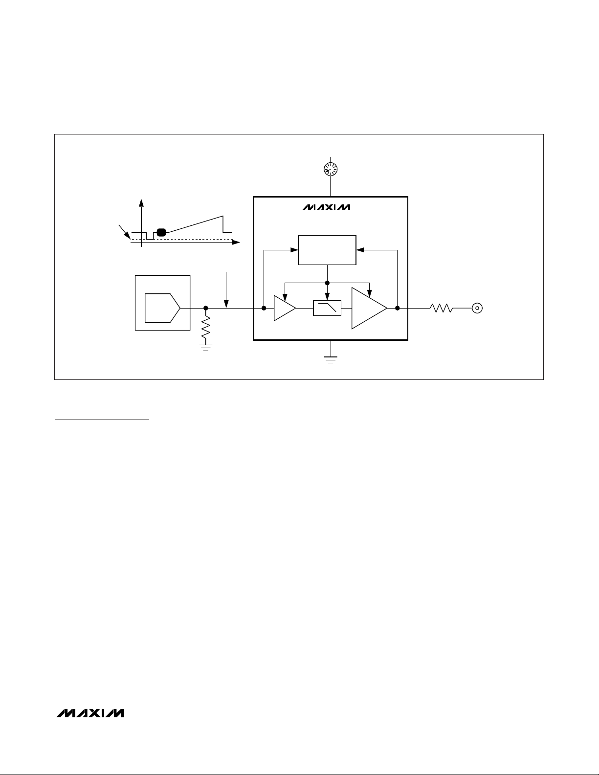
Detailed Description
The MAX9519 is an ultra-small, standard-definition video
filter amplifier with automatic shutdown. Automatic shutdown circuitry provides intelligent power management
by disabling the filter and output amplifier in the
absence of an input video signal and/or output load.
Figure 1 shows automatic shutdown.
An internal reconstruction filter smooths the steps and
reduces the spikes on the video signal from the video
digital-to-analog converter. The reconstruction filter typically has ±1dB passband flatness to 9MHz and typically 48.5dB of attenuation at 27MHz. The MAX9519
has an internal fixed gain of 4V/V and expects a nominal full-scale video input signal of 0.5V
P-P
.
Automatic Shutdown
The MAX9519 automatic shutdown circuitry reduces
power consumption when there is no active video input
signal or an output load. In shutdown, the supply current is reduced to 1.8µA. The video amplifier only turns
on when both an active video input signal and an output load are present.
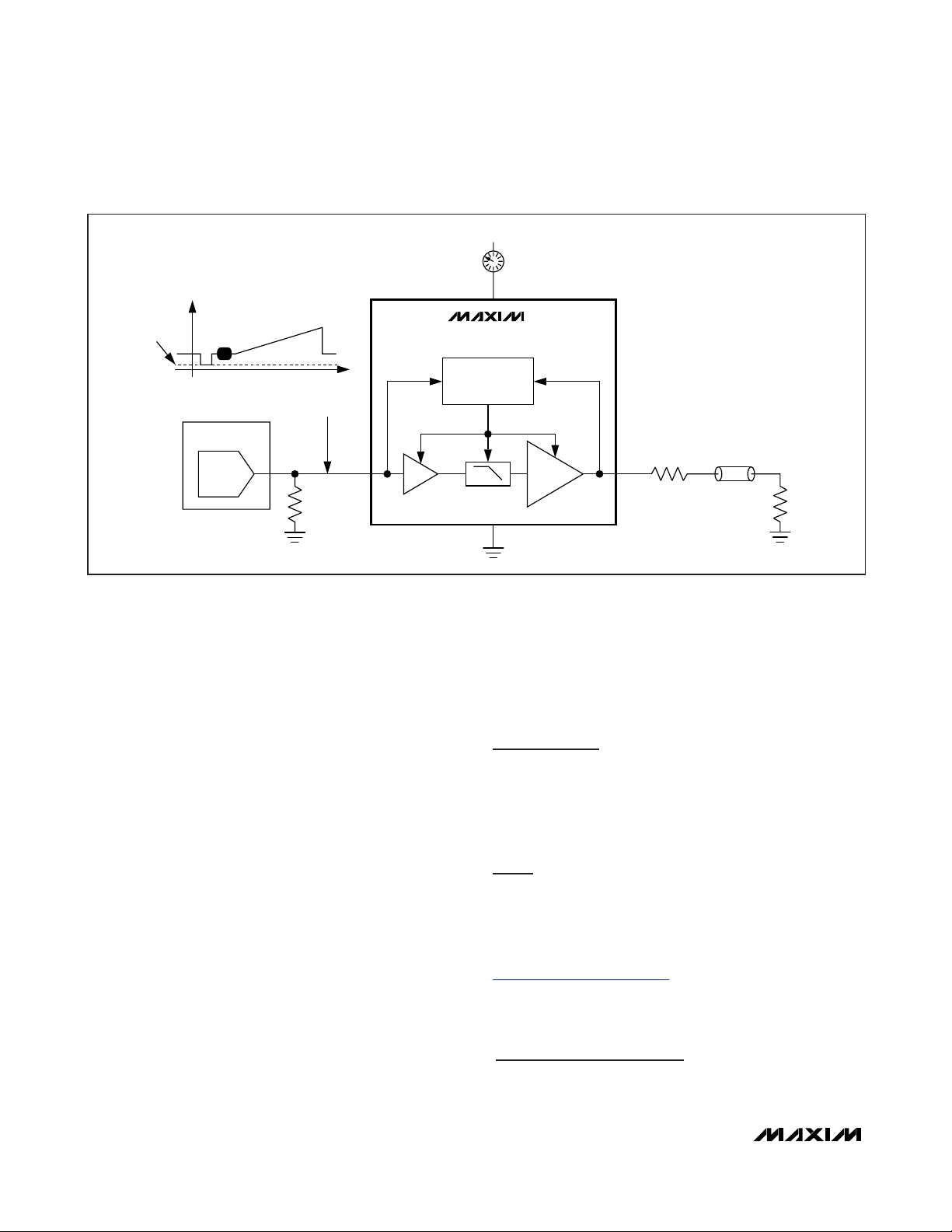
The MAX9519 slices the IN signal at 2.4% of the power
supply (80mV for a 3.3V supply). If the transitions occur
at a rate of 7.3kHz or higher, a video signal is present.
When the MAX9519 detects a video signal with sync at
the input, the control logic enters the active-detect mode
and enables the load sense circuitry (Figure 2). The supply current increases from 1.8µA to 5.4µA typically.
If an output load is not connected to the amplifier, the
MAX9519 remains in active-detect mode. Eight times
per second, the load-sense circuit checks for a load by
connecting an internal 15kΩ pullup resistor to the output for 1ms. If the output is pulled up, no load is present. If the output stays low, a load is connected.
If the input video signal is present and a load is connected to the output, the filter and amplifier turn on and
remain on until the output load is disconnected.
Automatic shutdown intelligently reduces the supply
current based on the input signal presence and output
loading (Figure 3).
When the amplifier is on, it continually checks if the
load has been disconnected by detecting if the amplifier output is sourcing current during a horizontal line
time. If no sourcing current is detected within one horizontal line time (approximately 64µs), the load has
been disconnected and the amplifier returns to activedetect mode. If, at any time, the input video signal is
removed, the MAX9519 returns to standby mode.
MAX9519
1mm x 1mm Video Filter Amplifier with
Automatic Shutdown and 4V/V Gain
_______________________________________________________________________________________ 7
0
Figure 2. Active-Detect Mode
TO
25mV
+3.3V
5.4μA
V
DD
VIDEO
0.5V
VIDEO ENCODER
CURRENT
DAC
P-P
VIDEO SIGNAL
PRESENT
IN
BUFFER
MAX9519
AUTOMATIC
SHUTDOWN
CONTROL LOGIC
LPF
GND
AV = 4V/V
OUT
75Ω
NO LOAD
Page 8
MAX9519
1mm x 1mm Video Filter Amplifier with
Automatic Shutdown and 4V/V Gain
8 _______________________________________________________________________________________
Input
The MAX9519 video input should be directly connected
to the output of the video current DAC. DC-coupling
ensures that the input signal is ground referenced such
that the sync tip of the composite video signal is within
25mV of ground. Any standard-definition video signal
can be applied to the input as long as the signal is
between ground and 0.525V when VDD= 2.7V.
Video Reconstruction Filter
The filter passband (±1dB) is typically 9MHz, which
makes the device suitable for standard-definition video
signals from all sources (e.g., broadcast and DVD).
Broadcast video signals are channel limited: NTSC signals have 4.2MHz bandwidth, and PAL signals have
5MHz of bandwidth. Video signals from a DVD player,
however, are not channel limited; so the bandwidth of
DVD video signals approaches the Nyquist limit of
6.75MHz. Recommendation: ITU-R BT.601-5 specifies
13.5MHz as the sampling rate for standard-definition
video. Therefore, the maximum bandwidth of the signal
is 6.75MHz. To ease the filtering requirements, most
modern video systems over sample by two times,
clocking the video current DAC at 27MHz.
Output
The MAX9519 output expects to drive a DC-coupled
load to ground. The amplifier output stage needs about
300mV of headroom from either supply rail. The device
has an internal level shift circuit that positions the sync
tip at approximately 300mV at the output.
Applications Information
Power-Supply Bypassing and Ground
The MAX9519 operates from a single-supply voltage
down to 2.7V, allowing for low-power operation. Bypass
VDDto GND with a 0.1µF capacitor. Place all external
components as close as possible to the device.
UCSP Applications Information
For the latest application details on UCSP construction,
dimensions, tape carrier information, PCB techniques,
bump-pad layout, and recommended reflow temperature profile, as well as the latest information on reliability
testing results, go to the Maxim’s website at
www.maxim-ic.com/ucsp to find the Application Note
1891:
Understanding the Basics of the Wafer-Level
Chip-Scale Package (WL-CSP).
CURRENT
DAC
VIDEO ENCODER
VIDEO SIGNAL
PRESENT
AV = 4V/V
OUTIN
BUFFER
LPF
AUTOMATIC
SHUTDOWN
CONTROL LOGIC
2.9mA QUIESCENT SUPPLY CURRENT NOT INCLUDING OUTPUT LOAD CURRENT
MAX9519
V
DD
+3.3V
75Ω
75Ω
GND
0
TO
25mV
0.5V
P-P
VIDEO
Figure 3. Full-Operation Mode
Chip Information
PROCESS: BiCMOS
Page 9

MAX9519
1mm x 1mm Video Filter Amplifier with
Automatic Shutdown and 4V/V Gain
Maxim cannot assume responsibility for use of any circuitry other than circuitry entirely embodied in a Maxim product. No circuit patent licenses are
implied. Maxim reserves the right to change the circuitry and specifications without notice at any time.
Maxim Integrated Products, 120 San Gabriel Drive, Sunnyvale, CA 94086 408-737-7600 _____________________
9
© 2008 Maxim Integrated Products is a registered trademark of Maxim Integrated Products, Inc.
Package Information
For the latest package outline information and land patterns, go to www.maxim-ic.com/packages.
MAX9519
PACKAGE TYPE PACKAGE CODE DOCUMENT NO.
4 UCSP R41A1+1
21-0242
2x2 UCSP.EPS
 Loading...